project final report · operation corresponds to a simple resistive two-state write-once-ready-many...
TRANSCRIPT

PROJECT FINAL REPORT
Grant Agreement number: 215132
Project acronym: PRIMEBITS
Project title: Printable memory solutions for sensor, ID, and media applications
Funding Scheme: Collaborative Project, Seventh Framework Programme, Theme 3
Period covered: from 2008 to 2010
Name of the scientific representative of the project's co-ordinator1, Title and Organisation:
Ari Alastalo, D.Sc.(Tech.), Senior Research Scientist, VTT, Teknologian tutkimuskeskus
Tel: +358 40 537 6198Fax: +358 20 722 7012
E-mail: [email protected]
Project websiteError! Bookmark not defined. address: http://www.primebits.eu/
1 Usually the contact person of the coordinator as specified in Art. 8.1. of the Grant Agreement.

Table of contents 1 Final publishable summary report .................................................................................................3
1.1 Executive summary................................................................................................................3 1.2 Project context and objectives ...............................................................................................4
1.2.1 WORM memories..........................................................................................................5 1.2.2 FRAM memories ...........................................................................................................5 1.2.3 Printing technologies .....................................................................................................5 1.2.4 Objectives ......................................................................................................................6
1.3 Main S&T results/foregrounds .............................................................................................. 77
1016202224262631333438
1.3.1 Electrically programmable WORM Memory ................................................................ 1.3.2 WORM Demonstrators ................................................................................................ 1.3.2 FRAM (Ferroelectric Read and Write) Memory .........................................................
1.4 Potential impact ................................................................................................................... References........................................................................................................................................ Supplementary material ...................................................................................................................
2 Use and dissemination of foreground .......................................................................................... 2.1 Section A (public) ................................................................................................................ 2.2 Section B (confidential) .......................................................................................................
2.2.1 Part B1 ......................................................................................................................... 2.2.2 Part B2 .........................................................................................................................
3 Report on societal implications....................................................................................................

1 Final publishable summary report
1.1 Executive summary Printed logic and memory is estimated to gain a significant market by the end of the current decade. Relevant application areas range from simple data-carrying cards to programmable RFID tags. The research and development efforts on different printable memory technologies have increased during the recent years with clear successes, for example, in mass fabricability, reliability, low-voltage operation and retention time. In the PriMeBits project the focus was on inorganic nanoparticulate metal and ferroelectric metal-oxide memory materials that have a potential to further improve the memory performance. The metal inks were used for write-once-read-many memories (WORM) and the ferroelectric materials were developed for read-and-write memories (FRAM). The WORM operation is based on the Rapid Electrical Sintering (RES) method invented by VTT. Here, the resistance of a metal nanoparticle conductor can be effectively electrically programmed. After printing and drying, a voltage is applied over the printed conductor which results in a rapid sintering of the nanoparticle structure and a related dramatic change in the conductivity. Thus, the operation corresponds to a simple resistive two-state write-once-ready-many memory (the low conductance "0" state vs. the high conductance "1" state). As the final resistance can be systematically and precisely controlled, an expansion to a multi-level operation is available to increase the memory capacity. For FRAM, the PriMeBits project investigated printed realizations of the traditional "hard" ferroelectric metal-oxide materials, such as BaTiO3. This is motivated by the low coercive field values characteristic of such displacive ferroelectric materials, especially in comparison with the fluoropolymers such as PVDF-TrFE. However, the processing (e.g., sintering) temperatures for these conventional metal-oxide materials are clearly beyond the thermal budgets of printed manufacturing. Therefore, the key target for the PriMeBits FRAM development was the formulation of a printable metal-oxide-composite. In addition to the memory technologies that have been developed for roll-to-roll mass printing, the PriMeBits project had a strong focus on the development of application demonstrations based on simple integration of printed electronics and sensors with reader infrastructures such as EPC RFID readers, sweep-over and contact readers. The publicly shown demonstrators included (i) questionnaire cards for customer feedback, (ii) ePINs for pass-code delivery, (iii) RFID coupled sensors with memory for permanent event storage, and (iv) value coupons such as lunch coupons with dynamic data. In 2010 the project had demonstrations in conferences: LOPE-C, RFID Europe, ICT 2010, Prinse seminar and the QUADRICA-PRODI workshop. The project partners are: VTT, Technical Research Centre of Finland, INM Leibniz Institut fur Neue Materialien GmbH, MidSweden University, Ecole Polytechnique Fédérale de Lausanne (EPFL), Sensible Solutions Sweden AB, Evonik Degussa GmbH, Motorola GmbH (until 28.2.2009), ARDACO, a.s., UPC Consulting Ltd. / UpCode Ltd., Stora Enso Oyj

1.2 Project context and objectives Printed memory is one of the technologies enabling printed-electronics (PE) products to enter market [1]. Inside the PE product scope, memory elements have a wide application range from self-standing concepts such as ID markings and brand-protection labels to being a crucial part of an integrated system such as an RFID tag or a programmable visual signboard. First applications of printed memories utilize static codes that are written during fabrication using digital printing such as inkjet. Such codes can only be read after fabrication but not written again for new content. Static codes have been utilized, for example, in the RFID tags of Kovio Inc. [2] and PolyIC GmbH [3] as well as in products of Nicanti [4] and Printechnologics [5, 6]. Nicanti is commercializing electrical codes and code readers for product security. Printechnologics is developing many of the applications identified also in the PriMeBits project such as access codes for digital content, marketing, brand protection, game cards and ticketing. Further applications and functionalities will be enabled by re-programmable memories such as the polymer ferroelectric memories of Thin Film Electronics (TFE) [7, 8] and the metal-oxide ferroelectric memories of PriMeBits. Such functionality is needed, for example, in games and RFID-coupled dynamic signage tags (e.g. price labels, see MariSense [9]).
In addition to the achievements discussed above that are closest to commercialization, there are also a few other recent activities developing memory concepts for flexible electronics. Mainly these can be grouped into (i) organic/polymer [10] and inorganic [11]–[13] resistance-change memories (ii) ferroelectric memories [14]–[16] or (iii) memories utilizing some other form of materials hysteresis such as that of thin film transistors [17] that often is attributed to interface charge trapping. In 2010, the MOMA EU project [18] started to address organic polymer memories. The PriMeBits project objectives were set both to the development of new roll-to-roll printable memory technologies and the development of application solutions based on simple integration of printed electronics and sensors with reader infrastructures such as EPC RFID readers, cellular phones, sweep-over and touch-point type reader pens. The main strategy was to utilize printed technology where it has a competitive advantage compared to silicon technology. Such areas include low-cost sensor probes, large-area sensor functions and combined printed read-only and read-and-write memory structures. The main intelligence and data processing was seen to be best included in the reader. The printed electronic circuit serves to collect data in space and time for later processing in reader devices. The primary functions needed for this is the printed sensor and the printed memory. There are at least three categories of solutions with different complexity and cost levels.
• Technology based on printed sensor probes that operate as a part of a reader device. • Technology based on printed sensor and memory being able to perform event detection and
counting without a reader device • Technology based on printed sensor, memory and data processing able to operate
independently but needing a reader for communication. For example, data logging and processing tags can be seen of this type.
Having all these different technology options at hand it is important to concentrate resources on bottleneck problems and enabling technologies. In PriMeBits project this was done by focusing the technology development on efficient mass-producable low-voltage memory solutions that enable printed-battery-operated write procedures. The memory development was focused in write-once-read-many (WORM) memories and on read-and-write ferroelectric (FRAM) metal-oxide memories.

1.2.1 WORM memories Printed WORM memories of PriMeBits are based on the electrical nanoparticle sintering method found at VTT [19, 20]. This method is based on an irreversible electrically-induced conductance change of a printed metallic nanoparticle structure. This fabrication technique works as follows. After drying off the carrier liquid to which the nanoparticles are dispersed in an ink, the printed structure consists of isolated nanoparticles that are coated with a polymer-based encapsulation material to prevent agglomeration. Normally such a structure is sintered thermally in an oven or using laser, UV or microwave radiation. During sintering the polymer coating is evaporated and the nanoparticles are adhered to each other to form a conductive overall structure. However, with either a thin polymer coating to enable tunnelling current in the non-sintered structure or if the coating is not a perfect insulator, it is possible to heat up the nanoparticle structure by passing either DC or AC current through the structure. As a fabrication method of printable electronics electrical sintering is attractive because i) it is fast (the sintering phase takes less than a second), ii) it reduces the thermal loading of the substrate because heat is concentrated only to the part being sintered and not to the whole structure, and iii) it enables direct online monitoring of the conductivity of the sintered line. Consequently, the electrical sintering method is of general interest in printable electronics not limited to memory applications.
1.2.2 FRAM memories The ferroelectric RAM (FRAM) can be implemented in two different ways either (i) as a capacitor the dielectric layer of which consists of ferroelectric material that possesses a permanent electric polarization that can point in two different directions corresponding to bit 1 and bit 0 or (ii) as a thin-film transistor with the ferroelectric material used in the gate dielectric. Because the printing resolution is much coarser (of the order of 100 µm) than the size of the nanoparticles (~ 100 nm), each bit contains a large number of nanoparticles or agglomerates. Thermally it is not possible to sinter this nanoparticle layer into a continuous structure on a flexible low-cost substrate because of the too high needed sintering temperatures (~ 1000 °C). For this reason, two different approaches were considered:
• The nanoparticles or agglomerates are not sintered but left isolated as indicated in. In this case, the random polarization directions of the nanoparticles somewhat reduce the attainable polarization in up-down direction.
• The nanoparticles are electrically sintered with AC voltage into a continuous structure. As discussed above, electrical sintering helps to reduce the thermal loading of the substrate because it concentrates the heat into the sintered material.
In either case, making a reliable electrical contact to the ferroelectric layer is one of the most critical challenges.
1.2.3 Printing technologies For the fabrication of the memory structures, several printing technologies can be applied. Each printing technology has pros and cons. From the ink development and fast prototyping point of view the most suitable printing methods are gravure and ink-jet due to the rather easy ink-development and easy printing process. However, big particle or agglomerate size (> 1 µm) will be a limiting factor for the usage of the ink-jet technology. Moreover, particle size also affects the minimum

feature size as well as the minimum achievable film thickness. Therefore effect of the size and the shape of the particles to the layer uniformity as well as to the functionality have to be investigated. In general it could be said that by using other printing technologies than ink-jet-printing the minimum line width lies around 50 µm. The minimum line width, however, depends greatly on the required film thickness resulting smaller features with lower film thicknesses and vice versa. Therefore, from the memory density and electrical properties point of view, lowering film thickness reduces the needed voltage for memory operations as well as increases the memory density but also set new requirements for the inks and registration of layers. Different printing processes require different type of ink properties. Gravure- and flexoprinting require typically viscosities from 50 cP to 500 cP whereas inks used in ink-jet have viscosities below 10 cP. Lower viscosity requirement leads easily to the sedimentation of non-suspended dispersions resulting problems during ink-jetting. Gravure- and flexoprinting on the other hand require certain amount of binder etc. to achieve good printability of the ink. Binders and other non-volatile additives decrease the amount of active particles in printed area. For the offset-printing, ink has to be hydrophobic and oily as well as it has to have viscosity in the range of thousands of cP’s. Such an ink is neither the first choice for new ink development purposes nor the ink for fast prototyping. Ink-, device- and manufacturing-methodology developments are made in a first stage by using laboratory scale printability tester machines. This is due to their low material consumption, fast testing of variables and ease of machine maintenance. All of these topics are much more demanding in a real R2R-environment. After table-top testing, manufacturing processes of multilayered WORM- and FRAM-memories can be transferred to a real R2R-environmentFor the roll-to-roll pilot fabrication of FRAM- and WORM-devices VTT’s pilot scale print facilities PICO and ROKO are used. Both machines are designed with a close co-operation with machine manufacturers and the machines are especially designed to fulfill requirements set by printed electronics. Manufacturing methodologies for example for printed OLEDs have been developed at VTT with these machines and in PriMeBits project manufacturing technology for all-R2R-printed WORM- and FRAM-components are developed with the help of these machines.
1.2.4 Objectives The objectives of the PriMeBits research project were • Develop new low-voltage large-area printable electronic memory devices to be utilized in new
and existing markets of printable smart tags for sensor, ID and media applications. • For the new memory solutions, develop printable materials (such as ferroelectric nanoparticle-
based inks) that also find applications outside the scope of the project such as in compact antennas and in tuneable capacitors for RFID.
• Develop the electrical sintering in a memory solution as a new manufacturing paradigm of printed electronics.
• Validate the feasibility of the developed solutions in printed systems through laboratory-scale prototyping and through end-user concept testing.
• Develop further the application scenarios, end-user concepts, business models and value chains for smart-package and smart-document applications utilizing the project results.
• Develop circuit-level models for the new components to be available for further work in the field of printed electronics.
• Disseminate the results into public knowledge, IPR and industry standards through various channels such as journal articles, patents and standard contributions.

1.3 Main S&T results/foregrounds
1.3.1 Electrically programmable WORM Memory To summarize the progress first briefly, the PriMeBits project was very successful in developing the WORM (write once read many) technology from the initial concept level to the roll-to-roll printing run that produced a large batch of memory cards to be extensively used in the demonstrator work. The electrically programmable WORM (Write Once Read Many) memory is based on the Rapid Electrical Sintering (RES) method developed by VTT [24, 25]. Here, the resistance of a printed metal nanoparticle conductor can be effectively electrically programmed. After printing and drying, a voltage is applied over the printed conductor which results in a rapid sintering of the nanoparticle structure and a related dramatic change in the conductivity. Thus, at simplest, the operation corresponds to a two-state memory (the high resistance "0" state vs. the low resistance "1" state). However, as the programmed resistance level can be systematically and precisely controlled via the applied electrical dose, an expansion to a multi-level operation is available to increase the memory capacity. In the first project phase, the development was done using inkjetted devices (Figure 1). The high-resolution structures made using commerically available silver nanoparticle inks from Advanced Nano Products (ANP) were used to determine the electrical writing parameters. As low-power operation (flexible batteries) was a central target for the developments, the write process power and duration vs. the device dimensions were systematically and successfully quantified. [26] [27]. As an example of the feasibility for low power operation, Figure 1 (a) shows the writing characteristic for the device illustrated in Figure 1 (b). Here, a 3V write voltage induced the three orders of magnitude resistance drop (from tens of kOhms to tens of Ohms) in 22 ms. The device in Figure 1 (b) was made using two inks: a single droplet of ANP DGH ink was deposited between ANP DGP single-droplet wide electrodes (DGH has a higher sintering temperature than DGP, which was utilized to obtain suitable initial resistance levels after thermal curing [28]). Figure 1 (c) shows another device type that was developed based on using only a single ink (ANP DGP). Here, the large contrast ratio between the bit and electrode resistances was obtained geometrically: the bit part was very narrow and thin (w ~ 25 µm, t ~ 300 nm) while the electrodes were made thick and wide. From all the inkjet devices, the electrical sintering writing energy was found to remain significantly smaller (typically 1/1000...1/100) than the energy required for breaking the bit (fuse operation), which thus forms a key advantage of the sintering approach for low-power applications.

(b) (C)(a)
g = 30 µm
w = 25 µm
DGPDGP DGH
Figure 1: The first generation WORM memory devices realized using inkjetting. Panel (a) shows the electrical writing characteristics for the two-layer device illustrated in Panel (b). At 3V write voltage, the write duration was 22 ms. Panel (c) shows a single-layer device . In (b), the electrodes and the bit were made using ANP DGP and DGH silver nanoparticle inks, respectively. In (c), the entire device was printed using ANP DGP ink. In the next project phase, the development effort was directed to roll-to-roll manufacturing of the WORM memories. Gravure printing was chosen as the printing method. A central challenge was how to reach the low write-operation power levels at the coarser device resolutions (bit size) that are accessible in gravure (and similar contact printing methods such as flexographic printing suited for roll-to-roll mass production). Here, a key breakthrough was made in the bit ink formulation [29] [30] which allowed significantly relaxed bit geometry sizes. Before roll-to-roll environment, the test devices were realized using desktop gravure printer (sheet-fed Labratester by Norbert Schläfli Machinen). Figure 2 an example of the produced memory banks where the bit dimensions were w ~ 100 µm, L ~ 200 µm. The electrical write process data shown in Figure 2 indicated that the devices could be written at Uwrite = 10V in less than 10 ms.
14‐bit gravure‐printed WORM memory bank.
L = 200 μm, w = 100 μm
Uwrite = 10 V and Rs = 330 Ω. Figure 2: The gravure-printed 14-bit WORM memory test bank and the electrical writing characteristics at Uwrite = 10V.

The WORM technology developments in the project culminated in the roll-to-roll gravure printing run performed at months 28-29 [31] [30]. As illustrated in Figure 3, the printing run was done at the ROKO-pilot printing machine at VTT. The two device layers, the bits and the electrodes, were printed in a single-pass run with automated registration (mutual alignment). The printed roll length exceeded 150 m. The produced roll was the roll-to-roll die-cut into memory cards (> 10 000 cards produced in total, several card types). Based on electrical characterization data, the best device types for demonstration purposes were identified. Standard hot-lamination (manual) was used to allow convenient handling of the samples for contact-reader demonstrator operation.
R2R-printing run of WORM memories:> 150 m printed length, > 10 000 memory cards, web speed 5 m/min, substrate 125 µm PET-foil (Melinex ST506)Single pass, two printed layers: electrically programmable bit and contact electrodes
VTT pilot printing line “ROKO” R2R die-cutter
1. Gravure printingof bits
2. Drying for 25 s at 140 C
3. Gravure printing
of contact electrodes
4. Drying for 25 s at 140 C
5. R2R die-cutting
of cards
6. Manual hot-lamination
ROKO R2R-printing line R2R die-cutter Sheet-fed hot laminator
Laminated WORM card Figure 3: The roll-to-roll WORM printing run performed in April-May 2010 at VTT. A critical aspect for the WORM memory performance is the long-term stability of the unsintered state resistance level. Regarding thermally-induced unwanted sintering during storage, the fundamental trade-off is between two factors: (1) the improved material stability gained via increased thermal sintering temperature, (2) the power budget for the electrically induced sintering process (write operation). In addition, other factors may influence the stability: in the case of the commercial silver nanoparticle inks employed for device realization in PriMeBits, we have observed clear humidity-induced resistance degradation. The stability results are shown in Figure 44. An excellent long-term stability for the gravure-printed samples was obtained when stored at room-temperature and low humidity conditions RH < 30 % (Figure 44 (a)). But when exposed to higher RH-levels and/or temperatures significant resistance decrease was observed (Figure 44 (b)). However, as the understanding has been developed for the material component inducing the RH-dependence, the subsequent ink formulation as part of commercialization effort should be well within reach to overcome this parasitic effect - combined with proper device sealing techniques which were as well not within the scope of PriMeBits.

From another perspective, the discovered humidity dependence was extensively exploited in the PriMeBits project in threshold alarm applications. Here, the WORM memory element was intentionally made moisture sensitive [32] - when exposed to moist conditions, the resistance level of the memory bit experienced a large, irreversible drop due to humidity-induced sintering. Thus, the usage of the non-volatile WORM memory enables detection of a past unwanted moisture condition even after the situation has changed (moisture is no longer present).
two months
(a)(b)
Figure 4: The long-term stability of the roll-to-roll printed WORM memories. Panel (a): The unsintered state resistance of the gravure-printed devices of Figure 2 remained constant at ambient conditions (non-encapsulated samples, stored in a plastic sleeve at 20 °C < T < 25 °C and 10 % < RH < 30 %). Panel (b) The unsintered state resistance of the roll-to-roll printed samples of Figure 3 when exposed to elevated temperature and humidity levels inside a climate chamber (manually hot-laminated samples). In particular, the elevated RH-levels are seen to induce resistance degradiation.
1.3.2 WORM Demonstrators Access codes To demonstrate the basic operation of the WORM memory cards in stand-alone application, a read&write USB-device was build (Figure 5). The device contains simple electronics that allow the readout and programming of the WORM memory cards via the user interface PC-software. In practice, the user inserts the memory card (the reader employs a standard Flexible Printed Circuit connector for the purpose), performs the readout of the card contents, selects the bit or bits to be written and triggers the write process, and reads the card content again to verify the successful write operation. The memory is non-volatile so that the card can be removed from the device and inserted again to re-read the content. Such electronic memory cards of ultra-low cost (disposable) can be utilized, for example, in access code applications: tickets, access to online services (WLAN access code, access to online content reserved for hardcopy purchasers, etc.). One such application demonstrator realized in PriMeBits is the Electronic Lunch Voucher shown in Figure 6.

memory card
Figure 5: The contact reader WORM demonstrator.
Figure 6: The Electronic Lunch Voucher demonstrar based on WORM memory.

Electronic questionnaire card The WORM memory banks were further used in the Electronic Questionnaire Cards ( Figure 7). Here, the card user answers the question by pressing a printed button which launches the write process of the corresponding bit in the WORM memory. The electrical action is powered by the integrated thin and flexible battery. Such a low-cost electrical questionnaire cards can be utilized, for example, at conferences to gather participant feedback or to vote for the best presentation/poster/exhibition booth.
WORM memory bank
Figure 7: The Electronic Questionnaire Card featuring the roll-to-roll printed WORM memory bank.

Moisture threshold alarm Figure 8 illustrates the WORM demonstrators realized for moisture detection applications (threshold alarm). In Figure 8 (a), the moisture sensitive WORM memory is integrated as part of the RFID antenna; the moisture-induced resistance drop in the WORM element changes the antenna properties so that the respective tag becomes visible / non-visible for the RFID reader [33]. The WORM-sensor tag is incorporated as an additional part of the Sensible Solutions TwinTag [34] solution. The standard Twin Tag contains two RFID tags: one of the tags has an antenna that is affected by moisture and the other acts as a reference (an unaffected antenna). The level of relative humidity is measured remotely by comparing the output power of the two tags using an UHF-RFID reader. However, the Twin Tag measures the current conditions and is unable to detect moisture conditions that are no longer present (but may have already triggered damage). Therefore, the addition of WORM-featured third tag, making the system thus Triple Tag, brings a key added value as it can record and reveal if specific humidity conditions have ever been exceeded. Commercialization of the technology is explored by Sensible Solutions. In Figure 8 (b), the WORM moisture sensor functionality is integrated as part of the EAS (Electronic Article Surveillance) tag. [35] Here, utilizing the widely available EAS reader infrastructure in retail, such a modified tag can be a cost-effective way for verification of product conditions (detection of damaged moisture-sensitive products).
(a) (b)
Figure 8: The WORM sensor demonstrators (moisture threshold alarm). Panel (a): the Triple Tag RFID-based moisture alarm system.Panel (b): the EAS (Electronic Article Surveillance) tag with integrated WORM threshold alarm function. Dynamic 2D barcode Here, the WORM memory controlled electrochromic display elements were utilized as additional bits of the 2D bar codes as shown Figure 9. Such an optical readout solution (cell phone) can be exploited in many of the WORM applications.

Figure 9: The dynamic 2D bar code demonstrator. Sweep-over readout The Nicanti [36] contactless technology was adapted in PriMeBits project for the readout of the WORM memory arrays [37] [38]. Figure 10 shows the setup used to demonstratre the readout of the electronic questionnaire memory content using the Nicanti reader. Figure 11 further shows the readout signal and the corresponding answers displayed on the user interface.
questionnaire
readercodes
user interface
Figure 10. The sweep-over reading setup of the memory elements used in the questionnaire card. Readout is done by sweeping the near-field Nicanti reader over the codes.

Figure 11. Sweep-over readout signal (top) and the corresponding questionnaire data on the user interface software (bottom).

1.3.2 FRAM (Ferroelectric Read and Write) Memory The starting point of PriMeBits FRAM development was to investigate the use of traditional "hard" ferroelectric metal-oxide materials, such as BaTiO3 in printed realizations. The main motivation for this stems from the high coercive field values in PVDF-TrFE polymer which is the state-of-the-art printed ferroelectric memory material [39]; at coercive fields approaching 100 V/µm, very thin PVDF-TrFE layers are needed to make the operation voltages reasonable (for example, 250 nm thickness requires above 20 V operation voltage [39]). In contrast to the stiff rotational switching character of the fluoropolymer chains in PVDF-TrFE, the crystalline ferroelectric materials such as BaTiO3 offer a greatly reduced coercive fields (0.001 ... 0.01 times the values for PVDF-TrFE depending of the degree of crystallinity). However, the conventional processing (e.g., sintering) temperatures exceed 1000 °C for these metal-oxide materials and are thus clearly beyond the thermal budgets of printed manufacturing and substrates. Therefore, the key target for the PriMeBits FRAM development was the formulation of an ink that benefits from the metal-oxide material fraction but can be cured at printing environment. A composite approach of metal-oxide nanoparticles embedded in a binder matrix was the chosen strategic guideline for the developments. The project successfully synthesized BaTiO3 nanoparticles (an example shown in Figure 12) with excellent ferroelectric properties [40] [41] and in quantities (tens of grams) suited for printing ink formulations. These refined particles were used in parallel with the commercially available BaTiO3 particles, dominantly from Inframat Advanced Materials LLC, USA.
Figure 12: TEM picture of the ferroelectric (c/a ~ 1.006, d ~ 80 nm) BaTiO3 nanoparticles synthesized.

The first composite formulation approach was based on dielectric binder materials such as and the sol-gel (εr = 14) matrix [42] and cyanoresin (εr ~ 18 by Shin-Etsu Corp., Japan) [40]. An example of the fully-printed test capacitor structures based on sol-gel matrix is shown in Figure 13. Another example of the test capacitor structures (non-printed electrodes) based on cyanoresin formulation at BaTiO3 volume loading fraction of ~60% is illustrated in Figure 14. Characteristic of these samples was the very high relative permittivities (εr ~ 90 (sol-gel) / 160 (cyanoresin)) and the capacitors tolerated high-field excitation (up to 100 V/µm). However, for memory applications the ferroelectric response was inadequate. The instantaneous remanent polarization extracted from the pulse train excitation response shown in Figure 14 (c) was a moderate Pi ~ 0.6 (1.3) µC/cm2 at excitation field Eex = 10 (25) V/µm, with similar values for the sol-gel matrix sample in Figure 13. Even more importantly, the polarization was not stable but decayed below 10% of the initial value within seconds for both sample types.
Pi = 1.1 0.1 µC/cm² (@ Eex = 25 V/µm)εr ~ 90 thickness FE layer ~ 7.0 µmvBT ≈ 50 vol.-%
Figure 13: The fully gravure-printed test capacitor where the ferroelectric layer was based on sol-gel BaTiO3 ink. The electrodes were printed using microparticle silver ink.

Sample 83. Kapton/Au/ BT (CR‐S) / Au‐evapo
(a)
(b)
(c)
100
50
0
-50
Exci
tatio
n [V
]
151050t [ms]
-3.0
-2.5
-2.0
-1.5
-1.0
-0.5
0.0
0.5
Response [V]
Figure 14: (a) The microscope image of the capacitor sample realized via gravure printing the BaTiO3 ink with cyanoresin binder on Au-metallized polyimide substrate. The BaTiO3 layer thickness was t ~ 9um. The top electrodes were evaporated Au dots (d ~210 um). (b) The C(V)-data of the capacitor sample showing clear hysteretic behavior when varying the DC-bias sweep direction. The extracted relative permittivity is εr ~ 160. (c) The capacitor response to electrical pulse train excitation. A clear difference between the switching and non-switching resposes is visible.

The fast decay of the stored polarization becomes well understandable in the light of the performed theoretical and simulation analysis. When surrounded by a dielectric, the ferroelectric high-permittivity BaTiO3 particles experience depolarizing fields (the compensating charge at the electrodes becomes screened by the low permittivity dielectric matrix) and the polarization back-flipping phenomena become viable. To stabilize the polarization, the project explored several strategies for the composite formulation. These included the improved connectivity between the ferroelectric particles via ceramic neck formation (low-temperature processing targeted via the Rapid Electrical Sintering (RES) process). While sintering of ferroelectric ceramics undoubtedly leads to stable ferroelectrics, the adoption of the RES process to e.g. BaTiO3 and to printed structures requires more effort. Supported by the theoretical and simulation analysis that a compensating charge can flow from the electrodes to stabilize the particle surfaces, the concept of adding a suitable amount of conductivity to the binder was followed, , however, without making the capacitor too leaky. The best results were obtained for the ferroelectric binder - in other words, the BaTiO3 - PVDF-TrFE composite. The BaTiO3 loading was kept at a low level (x = 20 and 10 %, respectively). Most notably, the good long-term stability and adequate polarization magnitude were obtained at excitation field of 50 V/µm. This marks a key achievement over the state-of-the-art printed ferroelectric memory based on pure PVDF-TrFE (a minimum of 70 V/µm was measured for stable operation of the pure PVDF-TrFE reference sample). The results of the piezo-force microscopy (PFM) studies made for the samples suggest that the switchable ferroelectric polarization originates from the PVDF-TrFE rather than the BaTiO3 particles. Therefore, at the low BaTiO3 loading factor (10..20 v-%) of these samples, the BaTiO3 nanoparticles role is to act as high-permittivity filler material reducing the effective layer thickness.

1.4 Potential impact Immediate expected industrial PriMeBits impact can be illustrated with the table showing the project demonstrators targeting different applications (see Table 1). Two of the demonstrated concepts – the Questionnaire Card and the Triple Tag – have proceeded into industrial piloting with clients. The ePINs and Lunch Coupons are being further analyzed by the partners for commercialization. Table 1: PriMeBits demonstrators.
PriMeBits Demonstrator Function # Read-
out Memory
Size Target
Application Stakeholders Demonstrated in 2010
Commercialization status
Building Mildew 1 UHF Transportation
Moisture
Sensible Solution
LOPE-C, RFID Europe Under piloting
2 EAS/LF Dry Package MIUN MSW2010 Being marketed
Sensor Threshold
Alarm
3 Barcode
1 bit WORM
Dynamic Barcode UpCode Project
internal To be
published
4 Contact ePIN /
Authentication / Lunch Coupon
MIUN / EPFL
(reader)
Under further analysis for
commercialization
5 Contact/Sweep
8-24 bit WORM
Compliance Card Stora Enso
LOPE-C, RFID Europe, ICT 2010, IOT 2010, IPI, OE-
A, Prinse seminar, Prodi
workshop Under piloting
IQ Cards for Gaming
Data Storage eCard
6 Contact 16 bit FRAM Loyalty Card for
Ticketing
VTT / EPFL (reader)
Project internal
To be published
Printed Electronics (PE) is expected to be among the fastest growing industries during the coming decades resulting in a high number of new jobs being created. Europe is the forefront of the field and since the investments needed for the fabrication facilities are much lower than in silicon industry, wealth creation can largely take place in the European countries where traditional strong industries, such as paper industry, are seeking new businesses. The growth rates of the PE industry are expected to be comparable to those of silicon industry in past. Namely, PE is expected to grow to a market size of 40 billion USD by 2020 as estimated by IDTechEx [22]. The main drivers of this development are (i) cost reduction of product fabrication, (ii) new enabled applications that need large area flexibility or other unconventional form factor and (iii) environmental friendliness of fabrication and products enabling disposability and recyclability. The logic memory market is expected to start significant growth after 2013 into one of the largest PE market shares. As reflected by the current state of the art, the overall printed memory development will proceed form the first-generation static memories programmed during fabrication via second-generation write-once-read-many (WORM) memories that can be electronically written after fabrication finally into third-generation memories that can be written several times. The PriMeBits memories fall into the second and third generations. The pioneer in the field of commercializing non-volatile printed read and write memories – Thin Film Electronics ASA – is heavily investing resources with their value-chain partners such as InkTec, PARC, PolyIC and Soligie to bring applications such as originality tags and dataloggers on market [23].
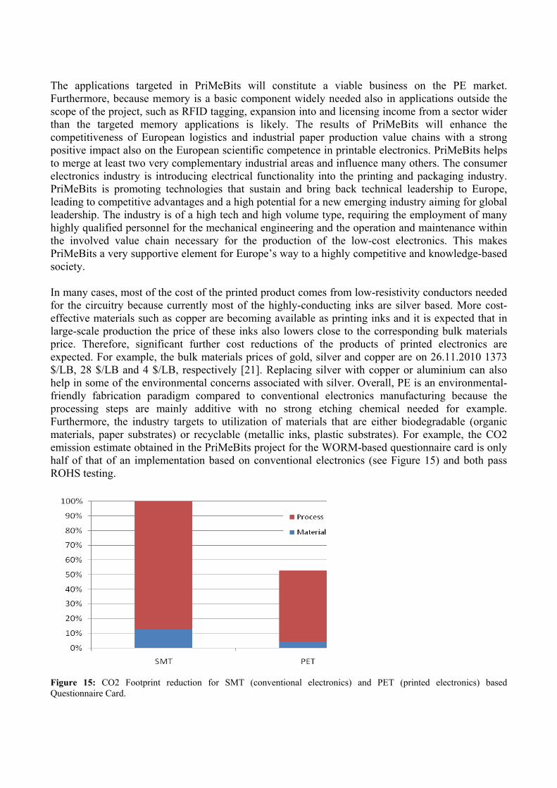
The applications targeted in PriMeBits will constitute a viable business on the PE market. Furthermore, because memory is a basic component widely needed also in applications outside the scope of the project, such as RFID tagging, expansion into and licensing income from a sector wider than the targeted memory applications is likely. The results of PriMeBits will enhance the competitiveness of European logistics and industrial paper production value chains with a strong positive impact also on the European scientific competence in printable electronics. PriMeBits helps to merge at least two very complementary industrial areas and influence many others. The consumer electronics industry is introducing electrical functionality into the printing and packaging industry. PriMeBits is promoting technologies that sustain and bring back technical leadership to Europe, leading to competitive advantages and a high potential for a new emerging industry aiming for global leadership. The industry is of a high tech and high volume type, requiring the employment of many highly qualified personnel for the mechanical engineering and the operation and maintenance within the involved value chain necessary for the production of the low-cost electronics. This makes PriMeBits a very supportive element for Europe’s way to a highly competitive and knowledge-based society. In many cases, most of the cost of the printed product comes from low-resistivity conductors needed for the circuitry because currently most of the highly-conducting inks are silver based. More cost-effective materials such as copper are becoming available as printing inks and it is expected that in large-scale production the price of these inks also lowers close to the corresponding bulk materials price. Therefore, significant further cost reductions of the products of printed electronics are expected. For example, the bulk materials prices of gold, silver and copper are on 26.11.2010 1373 $/LB, 28 $/LB and 4 $/LB, respectively [21]. Replacing silver with copper or aluminium can also help in some of the environmental concerns associated with silver. Overall, PE is an environmental-friendly fabrication paradigm compared to conventional electronics manufacturing because the processing steps are mainly additive with no strong etching chemical needed for example. Furthermore, the industry targets to utilization of materials that are either biodegradable (organic materials, paper substrates) or recyclable (metallic inks, plastic substrates). For example, the CO2 emission estimate obtained in the PriMeBits project for the WORM-based questionnaire card is only half of that of an implementation based on conventional electronics (see Figure 15) and both pass ROHS testing.
Figure 15: CO2 Footprint reduction for SMT (conventional electronics) and PET (printed electronics) based Questionnaire Card.

References [1] OE-A, Organic Electronics Association, “Organic and Printed Electrnics”, 3rd Edition, 2009 [2] www.kovio.com – US company developing printed RFID [3] www.polyic.com – German company developing printed tags [4] www.nicanti.com – a joint venture of VTT, Itaca Nova and Vera Venture. [5] www.printechnologics.com – a company formerly known as Menippos and receiving funding
from 3M. [6] Sascha Voigt, “Printechnologics – Real Printed Electronics”, Printed Electronics Asia 2010
conference. [7] www.thinfilm.se [8] Davor Sutija, “From stand-alone memory to printed systems”, Printed Electronics Asia 2010
conference [9] www.marisense.com [10] H.-T. Lin, Z. Pei, J.-R. Chen, and Y.-J. Chan, “A UV-erasable stacked diode-switch organic
nonvolatile bistable memory on plastic substrates,” IEEE Electron Device Lett., vol. 30, no. 1, pp. 18–20, 2009.
[11] J. Yun, K. Cho, B. Park, B. H. Park, and S. Kim, “Resistance switching memory devices constructed on plastic with solution-processed titanium oxide,” J. Mater. Chem., vol. 19, pp. 2082–2085, Feb. 2009.
[12] S. Kim, H. Moon, D. Gupta, S. Yoo, and Y.-K. Choi, “Resistive switching charateristics of sol-gel zinc oxide films for flexible memory applications,” IEEE Trans. Electron Devices, vol. 56, no. 4, pp. 696–699, Apr. 2009.
[13] J. W. Seo, J.-W. Park, K. S. Lim, S. J. Kang, Y. H. Hong, J.-H. Yang, L. Fang, G. Y. Sung, and H.-K. Kim, “Transparent resistive random access memory fabricated at room temperature,” Appl. Phys. Lett., vol. 95, p. 133508, Oct. 2009.
[14] T. Sekitani, K. Zaitsu, Y. Noguchi, K. Ishibe, M. Takamiya, T. Sakurai, and T. Someya, “Printed nonvolatile memory for a sheet-type communication system,” IEEE Trans. Electron Devices, vol. 56, no. 5, pp. 1027–1035, May 2009.
[15] M. Hasegawa, N. Kobayashi, S. Uemura, and T. Kamata, “Memory mechanism of printable ferroelectric TFT memory with tertiary structured polypeptide as a dielectric layer,” Synth. Met., vol. 159, pp. 961–964, May 2009.
[16] R. C. G. Naber, K. Asadi, P. W. M. Blom, D. M. de Leeuw, and B. de Boer, “Organic nonvolatile memory devices based on ferroelectricity,” Adv. Mater., vol. 22, pp. 933–945, Aug. 2009.
[17] Rodrigo Martins, Pedro Barquinha, Luís Pereira, Nuno Correia, Gonçalo Gonçalves, Isabel Ferreira, and Elvira Fortunato, “Write-erase and read paper memory transistor”, Applied Physics Letters, vol. 93, 203501 (2008).
[18] http://www.moma-project.eu/ [19] Heikki Seppä and Mark Allen, Patent Application FI 20060697 / US 60/832,144, July 21, 2006. [20] Jaakko Leppäniemi, et al., “Printed WORM-memory on Flexible Substrate Based on Rapid
Electrical Sintering of Nanoparticles”, IEEE Transactions on Electron Devices, v 58, n 1, January 2011
[21] www.metalprices.com [22] 66. Peter Harrop, IdTechEx, “Printed Electronics 2010 – 2020”, Proceedings of Printed
Electronics Europe 2010. [23] Davor Sutija, “From stand-alone memory to printed systems”, Printed Electronics Asia 2010
conference [24] H. Seppä and M. Allen, Finnish patent FI20060697. WO2008/009779A1, US2009301769,
CN101518164. [25] M. Allen, M. Aronniemi, T. Mattila, A. Alastalo, K. Ojanperä, M. Suhonen and H. Seppä,
Nanotechnology 19, 175201 (2008).

[26] J. Leppäniemi, M. Aronniemi, T. Mattila, A. Alastalo, M. Allen, and H. Seppä, “Printed WORM Memory on Flexible Substrate Based on Rapid Electrical Sintering of Nanoparticles”, IEEE Trans. Electron Dev. 58, 151 (2011).
[27] H. Andersson , A. Rusu, A. Manuilskiy, S. Haller, S. Ayöz, H-E Nilsson, "System of nano-silver inkjet printed memory cards and PC card reader and programmer", Microelectronics Journal 42, 21 (2011).
[28] T. Mattila, A. Alastalo, M. Allen and H. Seppä, "Electronics module, method for the manufacture thereof and applications", FI20075429, EP2001053, US2008303583, CN101325245.
[29] T. Mattila, T. Kololuoma, J. Leppäniemi, M. Allen, "Printed Memory Ink", VTT Invention Report KI 010145 (15 June 2010).
[30] J. Leppäniemi, T. Mattila, T. Kololuoma, A. Alastalo, "Roll-to-roll Gravure Printed Resistive WORM Memory on Flexible Substrate", manuscript to be submitted.
[31] Ari Alastalo, Tomi Mattila, Jaakko Leppäniemi, Mika Suhonen, Terho Kololuoma, Andreas Schaller, Henrik Andersson, Anatoliy Manuilskiy, Jinlan Gao, Hans-Erik Nilsson, Alexandru Rusu, Suat Ayöz, Igor Stolichnov, Simo Siitonen, Mikael Gulliksson, Johan Sidén, Tobias Lehnert, Jens Adam, Michael Veith, Alexey Merkulov, Yvonne Damaschek, Jürgen Steiger, Markus Cederberg, and Miroslav Konecny, ”Printable FRAM and WORM memories and their applications”, talk, paper and exhibition stand at LOPE-C 2010 conference, June 2010
[32] H. A. Andersson, A. Manuilskiy, T. Unander, C. Lidenmark, S. Forsberg, H-E. Nilsson, Inkjet printed silver nanoparticle humidity sensor on paper, submitted to Sensors and Actuators B.
[33] J. Gao, J. Sidén, H.-E. Nilsson and M. Gulliksson, Printed Moisture Sensor with Memory Functionality for Passive RFID Tags, submitted to IEEE Sensors Journal.
[34] H.-E. Nilsson, J. Siden, A. Koptioug, Sensor arrangement using RFID units, SE532227 (C2), WO 2008069753 (A1).
[35] H.-E. Nilsson, et al., “Printed Write Once and Read Many Sensor Memories in Smart Packaging Applications”, IEEE Sensors Journal, 2010, accepted
[36] Nicanti Oy. http://www.nicanti.com/. [37] M. Allen, A. Alastalo, J. Leppäniemi, T. Mattila, H. Seppä, FI20096341. [38] M. Allen et al., "Contactless read-out of printed memory", manuscript submitted to
Microelectronic Engineering on 17Dec2010. [39] N. Johansson, Thin Film Electronics: “Volume manufacturing of printed non-volatile
memories,” presented at the Printed Electronics, Asia, Tokyo, Japan, Oct. 1, 2009. [40] T. Lehnert, J. Adam, R. Drumm, J. Dietz, and M. Veith, Ferroelectric characterization of
isolated BaTiO3 particles, Ferroelectrics (accepted). [41] J. Adam et al, Ferroelectric polarisability of size and tetragonality varied BaTiO3 nanoparticles,
to be submitted. [42] T. Lehnert, P. Herbeck-Engel, J. Adam, G. Klein, T. Kololuoma and M. Veith, Dielectric
Properties of a Printed Sol–Gel Matrix Composite, Adv. Eng. Mat. 12, 379 (2010).

Supplementary material The project website at www.primebits.eu will be held serving for the years following the project period.
Partners
Short name
Country Name of technical contact(s)
Ari Alastalo
[email protected] Teknologian tutkimuskeskus VTT FI Tomi
Mattila [email protected]
INM Leibniz-Institut für Neue Materialien gGmbH
INM DE Jens Adam [email protected]
Mid Sweden University MIUN SE Hans-Erik Nilsson
Ecole Polytechnique Federale de Lausanne
EPFL CH Wladyslaw Grabinski
Sensible Solutions Sweden AB Sensible SE Mikael Gulliksson
Evonik Degussa GmbH Evonik DE Alexey Merkulov
ARDACO, a.s. Ardaco SK Miroslav Konecny
UPC Consulting Ltd. /UpCode Ltd.
UpCode FI Markus Cederberg
Stora Enso Oyj Stora FI Simo Siitonen
A few pictures taken during the project are shown below.

PriMeBits demonstrators at the VTT / Printocent stand in LOPE-C 2010. From left to right Kimmo Ojanperä, Jaakko Leppäniemi, Ari Alastalo, and Riikka Suhonen of VTT.
Sorting cutted samples of memory banks.

2 Use and dissemination of foreground
2.1 Section A (public) A major goal of the dissemination activity was to promote at international level the most visible and relevant advancements of PriMeBits in terms of printable memory demonstrators and scientific publications. As this is a very multidisciplinary project, the dissemination strategy encompasses the various communities that are involved in PriMeBits: nanoparticle synthesis, ink technology, printing techniques and applications. The dissemination activities were divided into four categories:
(i) setup and maintenance by EPFL (http://primebits.epfl.ch) of a dedicated website aimed to serve as an open web space for the external world to the Consortium and disseminate the public results obtained by the consortium;
(ii) publication of technical and scientific results in selected high-level international journals and conferences (as detailed later in this document);
(iii) demonstrations at industrial exhibitions
(iv) organization of PriMeBits workshops on printable memory technologies and their applications.
The scientific dissemination actions are summarized in the tables below. The research work and dissemination will continue after the project along the routes proved promising in the project to set the memory performance of printed electronics on a much higher level. Especially, the demonstrator work has been widely disseminated in:
• The first public PriMeBits WORM technology demonstration was successfully made at the LOPE-C conference (May-June 2010) in Frankfurt. At the VTT booth, the WORM demonstrations included the contact reader, the electronic questionnaire card and the sweep-over readout.
• RFID Europe Masterclass (Siitonen and Schaller, Cambridge Sep2010). A WORM questionnaire card was given to each participant (~20) of the class to provide their answers to the questions on the card
• In ICT 2010 in October in Brussels, VTT and Ardaco presented the questionnaire-card, ePIN, Tirple Tag and Lunch voucher demonstrators.
• EU Prodi Workshop (Mattila, Siitonen, Schaller, Munich Oct 2010). The programming and readout of the both stand-alone WORM card and the WORM electrical questionnaire card were demonstrated online to the audience.
• MRS Fall Meeting (J. Leppäniemi and A. Alastalo, Boston, Nov-Dec 2010). Oral presentations illustrated the WORM developments.
• Presentations and demonstrations have also been held in IOT 2010 conference, IPI Working Group Meeting, OE-A meetings and the Prinse seminar held organized by VTT for industry in November in Oulu Finland.
During the project the academic partners have gained a lot of experience in new research challenges and solutions of wide interest. This serves in future to disseminate the PriMeBits outcomes through teaching activities in order to educate new scientists to the field.

TEMPLATE A1: LIST OF SCIENTIFIC (PEER REVIEWED) PUBLICATIONS, STARTING WITH THE MOST IMPORTANT ONES
NO. Title Main author Title of the periodical or the series
Number, date or frequency
Publisher Place of publication
Year of publication
Relevant pages
Permanent identifiers2 (if available)
Is/Will open access3 provided to this publication?
1 Printed WORM-memory on Flexible Substrate Based on Rapid Electrical Sintering of Nanoparticles
Jaakko Leppäniemi
IEEE Transactions on Electron Devices
v 58, n 1, January
IEEE 2011 p 151-159 http://ieeexplore.ieee.org/stamp/stamp.jsp?arnumber=05635327
2 Printed Write Once and Read Many Sensor Memories in Smart Packaging Applications
H.-E. Nilsson IEEE Sensors Journal Accepted IEEE 2010 http://ieeexplore.ieee.org/stamp/stamp.jsp?tp=&arnumber=5648442
3 Dielectric Properties of a Printed Sol-Gel Matrix Composite
T. Lehnert Advanced Engineering Materials
12
Wiley 2010
379 …
http://onlinelibrary.wiley.com/doi/10.1002/adem.201000109/abstract
4 Modelling of Nanoparticle Sintering under Electrical Boundary Conditions
A. T. Alastalo Journal of Physics D: Applied Physics
v 43, n 48, December
IOP 2010 http://iopscience.iop.org/0022-3727/43/48/485501
5 Ferroelectric characterization of nondensified particle-based structures
T Lehnert
Journal of Applied Physics
vol. 106
AIP 2009 pp. 064108-1-5
http://jap.aip.org/japiau/v106/i6/p0
2 A permanent identifier should be a persistent link to the published version full text if open access or abstract if article is pay per view) or to the final manuscript accepted for publication (link to article in repository). 3 Open Access is defined as free of charge access for anyone via Internet. Please answer "yes" if the open access to the publication is already established and also if the embargo period for open access is not yet over but you intend to establish open access afterwards.

64108_s1?isAuthorized=no
6 Ferroelectric characterization of isolated BaTiO3 particles
T. Lehnert
Ferroelectrics
Accepted Taylor & Francis
2010
7 Contactless read-out of printed memory Mark Allen Microelectronic Engineering
Submitted Elsevier
8 System of nano-silver inkjet printed memory cards and PC card reader and programmer
Henrik Andersson
Microelectronics Journal
Submitted Elsevier
9 Inkjet printed silver nanoparticle humidity sensor on paper
Henrik A. Andersson
Sensors and Actuators B
Submitted Elsevier
10 Wireless Sensor Technology for Measurement of Urine Saturation in Diapers
H-E. Nilsson IEEE Sensors Journal Submitted IEEE
11 Printed Moisture Sensor with Memory Functionality for Passive RFID Tags
Jinlan Gao
IEEE Sensors Journal submitted IEEE
12 Printed Electromagnetic Coupler with Embedded Moisture Sensor for Ordinary Passive RFID Tags
Jinlan Gao
IEEE Electron Device Letters
To be submitted
IEEE
13 Ferroelectric polarisability of size and tetragonality varied BaTiO3 nanoparticles
J. Adam
To be submitted

TEMPLATE A2: LIST OF DISSEMINATION ACTIVITIES
NO. Type of activities4 Main leader Title Date Place Type of audience5 Size of audience
Countries addressed
1 Conference Jaakko Leppäniemi MRS Fall Meeting Nov. 29 - Dec. 3, 2010 Boston, USA Scientific Community
2 Conference Andreas Schaller IOT 2010 December 2010 Tokyo, Japan Industry 3 Conference S Siitonen RFID Europe 2010 27.09.2010 Cambridge, UK Industry / Scientific
Community
4 Conference A Schaller IPI Working Group Meeting 23.06.2010 London, UK Industry 5 Workshop J. Adam PRODI Workshop and Seminar 4.- 6. October 2010
Munich, Germany Industry
6 Conference Ari Alastalo ICT2010
27.-29., 2010
Brussels, Belgium Policy makers / Industry
7 Conference T. Lehnert 19th International Symposium on the Application of Ferroelectrics (ISAF)
10.-12. August 2010
Edinburgh, Scotland Scientific Community
8 Conference T. Lehnert Material Science and Engineering (MSE) 24. -26. August 2010
Darmstadt, Germany Scientific Community
9 Conference Tomi Mattila LOPE-C 2010 June 2010
Frankfurt, Germany Industry
10 Conference Andreas Schaller Energy Harvesting & Storage Wireless Sensor Networks & RTLS
26 - 27.05.2010
Munich, Germany Industry
11 Conference J. Adam PTS-Seminar 13.-14. April 2010 Munich, Germany Industry 12 Conference J. Adam Annual meeting of the German Ceramic
Society (DKG) 22.-24. March 2010
Hermsdorf, Germany
13 Workshop H-E Nilsson MSW2010
May 4.-5. 2010 Stockholm, Sweden Industry
14 Conference Andreas Schaller Smart Systems Integration Conference 23.-24. March 2010 Como, Italy Industry 15 Conference Ari Alastalo Printed Electronics Europe 2009 April 2009
Dresden, Germany Industry
16 Conference Ari Alastalo Nanomaterials 09 June 2009
Bonn, Germany Industry
17 Conference A Rusu 35th Int. Conf. on Micro- and Nano-Engineering
from 28 September to 1 October 2009
Ghent, Belgium Scientific Community
4 A drop down list allows choosing the dissemination activity: publications, conferences, workshops, web, press releases, flyers, articles published in the popular press, videos, media briefings, presentations, exhibitions, thesis, interviews, films, TV clips, posters, Other. 5 A drop down list allows choosing the type of public: Scientific Community (higher education, Research), Industry, Civil Society, Policy makers, Medias ('multiple choices' is possible.

18 Conference A Rusu Int. Semiconductor Conference (CAS) 2009
Date:12-14 Oct. 2009 Sinaia, Romania Scientific Community
19 Conference A Rusu ESSDERC 2010 13-17 September 2010 Sevilles, Spain Scientific Community
20 Conference A Rusu IEDM 2010 December 6-8, 2010 San Francisco, CA Scientific Community
21 Workshop J Adam IMST 2009 Sep 8-9, 2009 Aachen, Germany
Scientific Community
22 Conference P Helistö RFID Europe 2009 29th - 30th September 2009
Cambridge, UK Industry
23 Conference S Siitonen RFID Europe 2009 29th - 30th September 2009
Cambridge, UK Industry
24 Conference T Lehnert 8th ECerS Students’ Meeting December 2-5, 2009 Novi Sad, Serbia Scientific Community
25 Conference J Gao PIERS 2010 5-8 July 2010 Cambridge, USA Scientific Community

2.2 Section B (confidential) PriMeBits project includes partners from a wide variety of industries ranging from companies dealing with the research and development of ferroelectric materials to those that are closer to the consumer end whether in logistics or packaging. A plan has been set up in the project that provides vision for the technological implementation of PriMeBits output after the project (deliverable D6-3). In summary, Evonik Degussa from Germany is looking into commercialising BaTiO3 and other material formulation for printed electronics. Stora Enso from Finland is particularly interested in combining their printed electronics experience with PriMeBits technology in compliance cards for clinical trials. Sensible Solutions from Sweden is focused in developing in-wall moisture sensors for construction and insurance industry. UPC Consulting and UpCode is interested in optically readable 2-D bar codes that reflect the contents of an array of WORM type memory by means of ink that changes colour with voltage. Ardaco from Slovakia is planning on combining the licensed PDMark technology with the technologies developed within PriMeBits for improving the security, content identification and authentication of printed documents and tickets. The project groups have jointly developed demonstrators to test many of the above commercialisation ideas and they have been presented in a number of industrial conferences, exhibitions and other events as shown below in the tables. Clear continuation plans exists, especially for the questionnaire card, sensor tag and the lunch coupon as discussed in more detail below.
External Feedback of :
Sum of Revenue in M€ in 5 Years by Application
Figure 16: Market estimate of WORM based applications for different demonstrator cases of PriMeBits. External feedback was collected from the companies listed in the left lower corner.

Figure 17: Possible players of printed electronics memory market along a value chain.
The market size available for the memories in the different applications demonstrated in the PriMeBits project was analyzed by Andreas Schaller Consulting (VTT subcontractor in PriMeBits) as shown in Figure 16. These estimates are for the first 5 years of commercial production with growing numbers towards the later years. For example, for the compliance/questionnaire-card application, a conservative estimate of the PE product cost is about 40 % of the silicon-based solution. The PriMeBits analysis is the basis of the interest of Stora Enso in the PE products. Breakthrough of the targeted application on commercial market will need several partners along a value chain. Potential partners can be identified as illustrated in Figure 17.

2.2.1 Part B1
TEMPLATE B1: LIST OF APPLICATIONS FOR PATENTS, TRADEMARKS, REGISTERED DESIGNS, ETC.
Type of IP Rights6:
Confidential Click on YES/NO
Foreseen embargo date dd/mm/yyyy
Application reference(s) (e.g. EP123456)
Subject or title of application Applicant (s) (as on the application)
Patents YES FI20096341 Programmable printed electric code, method of manufacturing the same and a programming device
Ari Alastalo, Mark Allen, Tomi Mattila, and Heikki Seppä
Several innovations exist in the project foreground for FRAM that after optimizing the solution will lead to protecting of IPR.
6 A drop down list allows choosing the type of IP rights: Patents, Trademarks, Registered designs, Utility models, Others.

2.2.2 Part B2
Type of Exploitable Foreground7
Description of
exploitable foreground
Confidential Click on YES/NO
Foreseen embargo
date dd/mm/yyy
y
Exploitable product(s) or measure(s)
Sector(s) of application8
Timetable, commercial or any other use
Patents or other IPR exploitation (licences) Owner & Other
Beneficiary(s) involved
Commercial exploitation of R&D results
R2R gravure printed low-voltage WORM memories
YES 1. Printed questionnaire card 2. Programmable optical code 3. LUNCH/GIFT COUPON
1. Market Research 2 .Information Services 3. PROTECTION OF VALUABLE DOCUMENTS 4. MONETARY SECTOR
2011
Memory patent is applied in 2009 by VTT
Stora Enso, VTT, Ardaco, UpCode
Commercial exploitation of R&D results
MOISTURE SENSITIVE WORM MEMORIES
YES TRIPLE TAG RFID MOISTURE SENSOR TAG
1. BUILDING MAINTAINANCE 2. LOGISTICS MONITORING
2011 SENSIBLE SOLUTIONS, MIUN
General advancement of knowledge
KNOWLEDGE ON FERROELECTRICITY OF NANOPARTICLE COMPOSITES
NO SCIENTIFIC ARTICLES
1. PRINTED ELECTRONICS
2011 INM, VTT, EVONIK, EPFL
More details of the applications of the above table are discussed below and in further detail in deliverable D6-3.
19 A drop down list allows choosing the type of foreground: General advancement of knowledge, Commercial exploitation of R&D results, Exploitation of R&D results via standards, exploitation of results through EU policies, exploitation of results through (social) innovation. 8 A drop down list allows choosing the type sector (NACE nomenclature) : http://ec.europa.eu/competition/mergers/cases/index/nace_all.html

Questionnaire Card Its purpose: In questionnaire card application low-voltage WORM memories can be used to store data to physical device with simple user interface without access to computers or internet. Low-voltage operation of memories enable use of totally printed solutions and spreads possibilities of data gathering. How the foreground might be exploited, when and by whom: This simple electronic questionnaire can be used to collect any kind of feedback which should be collected offline. The questionnaire can be added easily to any kind of product packaging or simple card can give much more information about feedback collection as all of its surfaces are printable and easily changeable depending on use case. During 2010 Stora Enso Packaging business area has started Intelligent Healthcare Packaging which has specialized developing, producing and commercializing intelligent paper and paper board packaging products in healthcare sector. One option to exploit this technology is to create fully printed healthcare questionnaires to be added into medication packaging or as separate cards given with medication. IPR exploitable measures taken or intended: Stora Enso has access to IPR which is related to traditional electronics based intelligent medication packaging and questionnaire cards. VTT has patented electrical sintering and gravure printed low-voltage memories and these should be licensed to start exploitation of the application. Further research necessary, if any: Low-voltage operation of memory bits must be developed further and stability of bits must be improved. At the moment there either no logic or other methods to control false answering and each bit requires own readout pin. This reduces possible use cases as number of bits is limited by readout connector. In future development work use of printed logic will be studied. Also mass manufacturing processes, especially assembly, will be developed further. Potential/expected impact (quantify where possible): Low-voltage WORM memory is one of key enabling technologies on a way to fully printed intelligent systems. When considering markets for questionnaire cards it must be remembered that solution can be used to collect any kind of feedback and is not limited to any specific use. But to illustrate market potentials a specific use in clinical trials has been studied. In clinical trials, compliance control is followed up by a questionnaire and/or diary filled in by the test persons while an automatic registration would offer more reliable information. The additional price is well covering the added value by the automated compliance control. The biggest clinical trials company runs 2000 trials/year which corresponds to 40% of the US market. According to them, 15% will be moved to smart packaging immediately when solutions are available and the capacity is reliable. This would correspond to 900000 packages/a for one clinical trials customer. Aiming at a sales price of 5€ per card this would yield an annual turn-over of 4.5 million € for one clinical trials customer only. This level could be assumed to be realistic to achieve in the whole world in few years. In prescription market, it would be especially the high value pharmaceuticals with time-sensitive effect which would be able to cover the additional cost, like for HIV medication, heart diseases, or diabetes, for example. This would increase the over all volume significantly.
Triple Tag Purpose of technology: If a moisture sensitive worm memory is added to the conventional Twin Tag of Sensible Solution, a moisture event occurring outside the time window of a momentous read-out, can be detected. Thus such a single event moisture threshold memory (Worm) is adding functionality and possibly value to this type of passive moisture status transponder. Foreground exploitation: The moisture sensitive Worm technology can be utilized and field tested by Sensible Solutions as soon as current customers of the Twin Tag set up have evaluated that technology in long term tests. This will probably be the case end of 2011. IP measures taken or intended: A national patent (Sweden) has been granted (2010) for the Twin tag set up. This patent is forming the IP background of a transponder arrangement with a moisture sensitive Worm memory. No additional IP measures will be initiated by sensible Solutions until market and long term tests has been evaluated. Further research: Verification of stability of the moisture worm, production method as well as attachment of the memory is still under evaluation. Expected commarcial impact: Limited number of moisture sensitive tags in evaluation programs with selected industrial partners during 2011. If test results prove robust functionality, production of Worm supplied transponders will be set up during 2012. Lunch/Gift Coupon Purpose: The purpose of Lunch/Gift coupon application is to propose new security features and user comfort to processing of paper coupons. The application is based on printed memory invented in PriMeBits project attached to paper coupons used in canteens in Slovakia. Both Lunch/Gift coupons applications need to be verified in small scale pilot projects. How the foreground might be exploited, when and by whom: The Lunch/Gift coupon application will be exploited via partnership with coupon issuer companies and counting machines providers. A common pilot project will be created in order to make a presentation to potential customers and to verify user comfort and usability. Ardaco will seek to create strong partnerships and to start the commercialization process within 1 year from the termination of PriMeBits. IPR exploitable measures taken or intended: VTT background as well as VTT and MIUN foreground of WORM memories. Ardaco foreground of application idea and implementation Further research: A non-contact magnetic readout would be beneficial for the purpose of pilot project and further exploitation. An increased memory capacity offers more security possibilities. Potential/expected impact: This depends on pilots and first user feedbacks. Now we are at the stage of experimental demonstrator showing possibility to adopt WORM in lunch/gift ticket industry. Programmable optical code Its purpose: To enable readout of the contents of printed memory with 2D-code reader. How the foreground might be exploited, when and by whom: It can be exploited by UpCode to add functionality to our existing logistics system.

IPR exploitable measures taken or intended: Only already existing patents regarding UpCode reader technology so far. Further research necessary, if any: Sensors for writing the memory need to be developed (currently the demonstrator uses switches for programming), and also higher capacity printed batteries to make writing of the memory more reliable. Potential/expected impact: Potentially gives the possibility to market the UpCode system as a combined sensor/tracking solution.

3 Report on societal implications
A General Information (completed automatically when Grant Agreement number is entered.
Grant Agreement Number: 215132
Title of Project: Printable memory solutions for sensor, ID, and media applications
Name and Title of Coordinator: Ari Alastalo, D.Sc. (Tech.)B Ethics
1. Did your project undergo an Ethics Review (and/or Screening)?
• If Yes: have you described the progress of compliance with the relevant Ethics
Review/Screening Requirements in the frame of the periodic/final project reports? Special Reminder: the progress of compliance with the Ethics Review/Screening Requirements should be described in the Period/Final Project Reports under the Section 3.2.2 'Work Progress and Achievements'
No
2. Please indicate whether your project involved any of the following issues (tick box) :
No
RESEARCH ON HUMANS • Did the project involve children? • Did the project involve patients? • Did the project involve persons not able to give consent? • Did the project involve adult healthy volunteers? • Did the project involve Human genetic material? • Did the project involve Human biological samples? • Did the project involve Human data collection?
RESEARCH ON HUMAN EMBRYO/FOETUS • Did the project involve Human Embryos? • Did the project involve Human Foetal Tissue / Cells? • Did the project involve Human Embryonic Stem Cells (hESCs)? • Did the project on human Embryonic Stem Cells involve cells in culture? • Did the project on human Embryonic Stem Cells involve the derivation of cells from Embryos?
PRIVACY • Did the project involve processing of genetic information or personal data (eg. health, sexual
lifestyle, ethnicity, political opinion, religious or philosophical conviction)?
• Did the project involve tracking the location or observation of people? RESEARCH ON ANIMALS
• Did the project involve research on animals? • Were those animals transgenic small laboratory animals? • Were those animals transgenic farm animals? • Were those animals cloned farm animals? • Were those animals non-human primates?
RESEARCH INVOLVING DEVELOPING COUNTRIES • Did the project involve the use of local resources (genetic, animal, plant etc)? • Was the project of benefit to local community (capacity building, access to healthcare, education
etc)?
DUAL USE • Research having direct military use No • Research having the potential for terrorist abuse

C Workforce Statistics 3. Workforce statistics for the project: Please indicate in the table below the number of
people who worked on the project (on a headcount basis). Type of Position Number of Women Number of Men
Scientific Coordinator 1 Work package leaders 7 Experienced researchers (i.e. PhD holders) 2 21 PhD Students 5 9 Other 11 26
4. How many additional researchers (in companies and universities) were recruited specifically for this project?
3
Of which, indicate the number of men:
2

D Gender Aspects 5. Did you carry out specific Gender Equality Actions under the project?
Yes No
6. Which of the following actions did you carry out and how effective were they? Not at all
effective Very
effective
Design and implement an equal opportunity policy Set targets to achieve a gender balance in the workforce Organise conferences and workshops on gender Actions to improve work-life balance Other:
7. Was there a gender dimension associated with the research content – i.e. wherever people were the focus of the research as, for example, consumers, users, patients or in trials, was the issue of gender considered and addressed?
Yes- please specify
No
E Synergies with Science Education
8. Did your project involve working with students and/or school pupils (e.g. open days, participation in science festivals and events, prizes/competitions or joint projects)?
Yes- please specify
No
9. Did the project generate any science education material (e.g. kits, websites, explanatory booklets, DVDs)?
Yes- please specify
No
F Interdisciplinarity
10. Which disciplines (see list below) are involved in your project? Main discipline9: 1.2 Physical sciences Associated discipline9:
1.3 Chemical sciences Associated discipline9:
2.2 Electrical engineering, electronics
G Engaging with Civil society and policy makers 11a Did your project engage with societal actors beyond the research
community? (if 'No', go to Question 14)
Yes No
11b If yes, did you engage with citizens (citizens' panels / juries) or organised civil society (NGOs, patients' groups etc.)?
No Yes- in determining what research should be performed Yes - in implementing the research Yes, in communicating /disseminating / using the results of the project
9 Insert number from list below (Frascati Manual).

11c In doing so, did your project involve actors whose role is mainly to organise the dialogue with citizens and organised civil society (e.g. professional mediator; communication company, science museums)?
Yes No
12. Did you engage with government / public bodies or policy makers (including international organisations)
No Yes- in framing the research agenda Yes - in implementing the research agenda Yes, in communicating /disseminating / using the results of the project
13a Will the project generate outputs (expertise or scientific advice) which could be used by policy makers?
Yes – as a primary objective Research and Innovation Yes – as a secondary objective Environment
No
13b If Yes, in which fields? Agriculture Audiovisual and Media Budget Competition Consumers Culture Customs Development Economic and Monetary Affairs Education, Training, Youth Employment and Social Affairs
Energy Enlargement Enterprise Environment External Relations External Trade Fisheries and Maritime Affairs Food Safety Foreign and Security Policy Fraud Humanitarian aid
Human rights Information Society Institutional affairs Internal Market Justice, freedom and security Public Health Regional Policy Research and Innovation Space Taxation Transport

13c If Yes, at which level? Local / regional levels National level European level International level
H Use and dissemination
14. How many Articles were published/accepted for publication in peer-reviewed journals?
6
To how many of these is open access10 provided? -
How many of these are published in open access journals?
How many of these are published in open repositories?
To how many of these is open access not provided? 6
Please check all applicable reasons for not providing open access: publisher's licensing agreement would not permit publishing in a repository no suitable repository available no suitable open access journal available no funds available to publish in an open access journal lack of time and resources lack of information on open access other11: ……………
15. How many new patent applications (‘priority filings’) have been made? ("Technologically unique": multiple applications for the same invention in different jurisdictions should be counted as just one application of grant).
1
Trademark -
Registered design -
16. Indicate how many of the following Intellectual Property Rights were applied for (give number in each box).
Other -
17. How many spin-off companies were created / are planned as a direct result of the project?
1
Indicate the approximate number of additional jobs in these companies: 1
18. Please indicate whether your project has a potential impact on employment, in comparison with the situation before your project:
Increase in employment, or In small & medium-sized enterprises Safeguard employment, or In large companies Decrease in employment, None of the above / not relevant to the project Difficult to estimate / not possible to quantify
19. For your project partnership please estimate the employment effect resulting directly from your participation in Full Time Equivalent (FTE = one person working fulltime for a year) jobs:
Indicate figure: 34
10 Open Access is defined as free of charge access for anyone via Internet. 11 For instance: classification for security project.

Difficult to estimate / not possible to quantify
I Media and Communication to the general public
20. As part of the project, were any of the beneficiaries professionals in communication or media relations?
Yes No
21. As part of the project, have any beneficiaries received professional media / communication training / advice to improve communication with the general public?
Yes No
22 Which of the following have been used to communicate information about your project to the general public, or have resulted from your project?
Press Release Coverage in specialist press Media briefing Coverage in general (non-specialist) press TV coverage / report Coverage in national press Radio coverage / report Coverage in international press Brochures /posters / flyers Website for the general public / internet DVD /Film /Multimedia Event targeting general public (festival, conference,
exhibition, science café)
23 In which languages are the information products for the general public produced?
Language of the coordinator English Other language(s)