projects audio pax – a power amplifier with error correction 2008040241... · projects audio 26...
TRANSCRIPT
projects audio
24 elektor - 4/2008
paX – a Power Amplifier with Error CorrectionPart 1: EC and the output stageJan Didden
Most solid state power amplifiers employ some form of global negative feedback to reduce non-linearities and output impedance. In some cases, designers exploit alternatives like feedforward to circumvent perceived disadvantages of global negative feedback. The present design uses error correction as (re)defined by Malcolm Hawksford around 1984 [1].
In part 1 of this article the author dis-cusses error correction for audio am-plifiers and presents an audio output stage based on error correction. Part 2 will extend the principle to the voltage amplifier stage and present a complete error correction power amplifier. In a separate article next month the pro-tection circuitry is discussed in more detail.
Negative feedback is not negativeThis is not an article against negative feedback (nfb). Negative feedback, as a general principle, is one of the most powerful tools available to the designer to build amplifiers that are transparent to the signal they amplify. With that I mean that they do not add anything to, or subtract from, the input signal. In reality, circuits are never ideal, but the changes to the signal can be made so small that inaudibility of the change is pretty much guaranteed.Negative feedback is also fully under-stood, and although bad-sounding feedback amplifiers are still being sold, it is totally unnecessary. So, you may ask, why bother with error correction
(ec)? For one thing, it is different; and different roads to the same goal are often enjoyable to travel and explore. Secondly, although we will see that ec is in many respects another face of nfb, with similar advantages and disadvan-tages, there are some interesting differ-ences and different challenges leading to better understanding of the process-es inside any feedback amplifier.
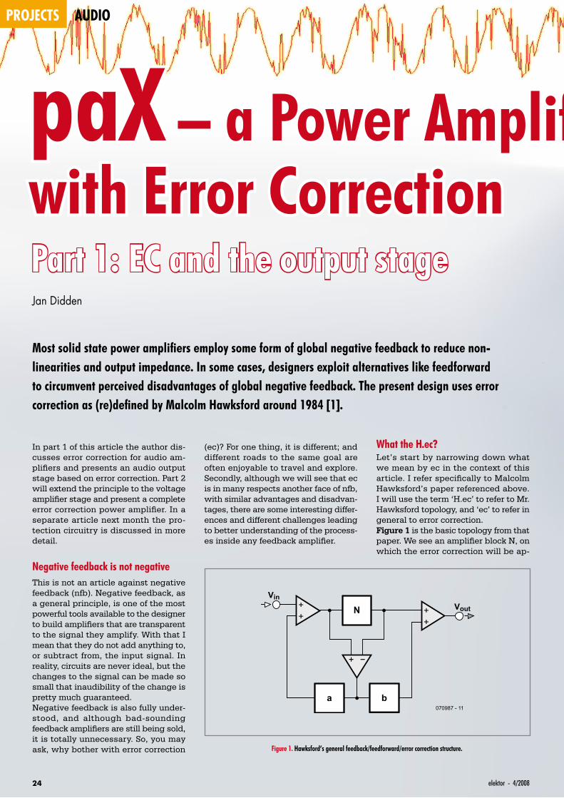
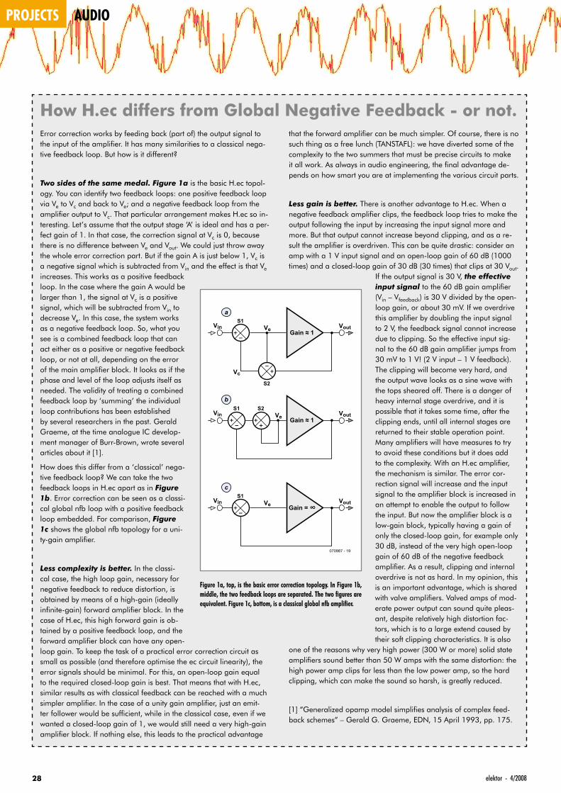
What the H.ec?Let’s start by narrowing down what we mean by ec in the context of this article. I refer specifically to Malcolm Hawksford’s paper referenced above. I will use the term ‘H.ec’ to refer to Mr. Hawksford topology, and ‘ec’ to refer in general to error correction.Figure 1 is the basic topology from that paper. We see an amplifier block N, on which the error correction will be ap-
N
a b
Vin
Vout
070987 - 11
Figure 1. Hawksford’s general feedback/feedforward/error correction structure.
254/2008 - elektor
paX – a Power Amplifier with Error Correction
plied. The difference between the input and output of that amplifier is either added to the input via block ‘a’ (error feedback), or to the output via block ‘b’ (error feedforward). All the summing and differencing blocks have unity gain (1×). Of course it is important that the error correction signal is added in just the right proportion to cancel the original error. In this design I use the correction via block ‘a’, added to the
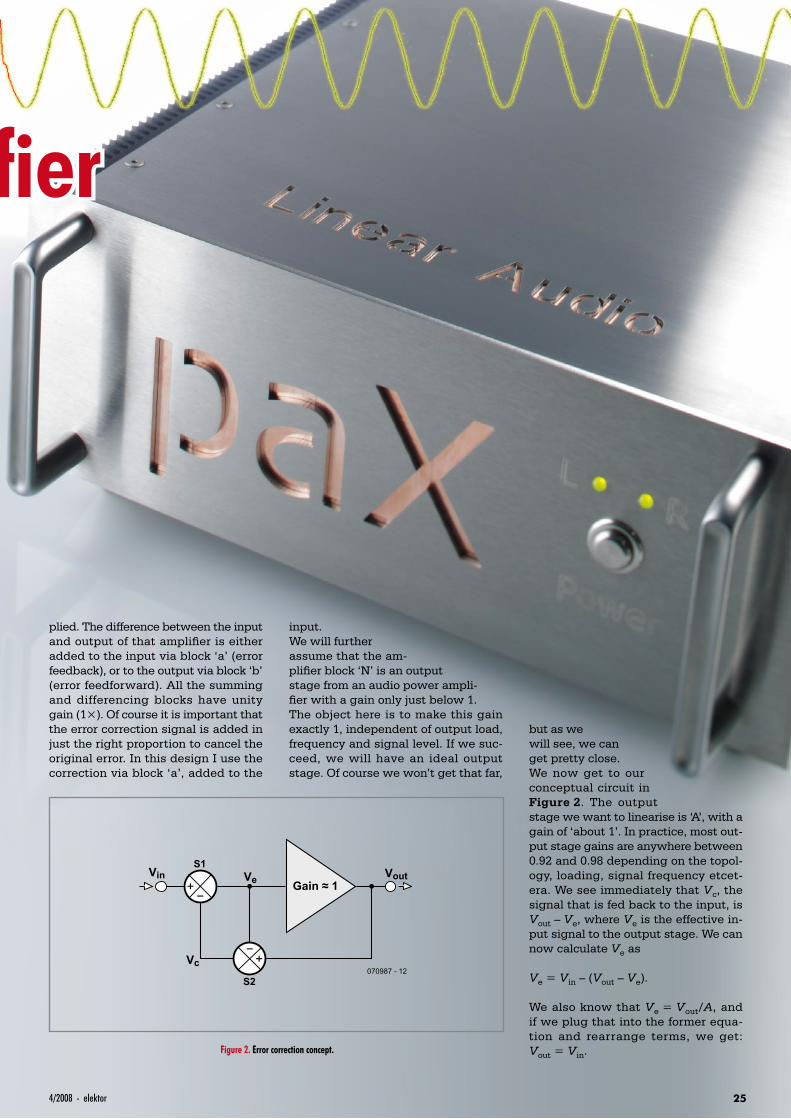
input. We will further assume that the am-plifier block ‘N’ is an output stage from an audio power ampli-fier with a gain only just below 1.The object here is to make this gain exactly 1, independent of output load, frequency and signal level. If we suc-ceed, we will have an ideal output stage. Of course we won’t get that far,
but as we will see, we can get pretty close.We now get to our conceptual circuit in Figure 2. The output stage we want to linearise is ‘A’, with a gain of ‘about 1’. In practice, most out-put stage gains are anywhere between 0.92 and 0.98 depending on the topol-ogy, loading, signal frequency etcet-era. We see immediately that Vc, the signal that is fed back to the input, is Vout – Ve, where Ve is the effective in-put signal to the output stage. We can now calculate Ve as
Ve = Vin – (Vout – Ve).
We also know that Ve = Vout/A, and if we plug that into the former equa-tion and rearrange terms, we get: Vout = Vin.
Vin Ve
Vc
S1
S2
Vout
070987 - 12
Gain ≈ 1
Figure 2. Error correction concept.
projects audio
26 elektor - 4/2008
What is significant here is that the actual amplifier gain A is no longer part of the equation. Whatever the short-comings, non-linearities or er-rors of A, we got rid of all of those. This is our ideal output stage!
If you are familiar with practi-cal audio amplifiers, you prob-ably are feeling a bit uneasy now. An ideal power stage? That would be the first one ever! And you are right — in reality, we can’t make that ideal.
The reason is that we as-sumed that the summers in Figure 2 are ideal summers, without flaws. That cannot be. Those summers consist of passive and (most probably) active devices that have their own non-linearities, so the ba-sic accuracy will not be ideal. Their characteristics will also vary with frequency, so the correction accuracy will vary with frequency. As the out-put stage gain will also vary with frequency and load, the amount of correction required will vary with frequency and load, meaning that signal lev-els in the summers vary with frequency and load as well. This further leads to accura-cy limitations.Nevertheless, it is possible to greatly improve the performance of the output stage with relative simple means, as we will see.
Thermal memoriesThere was one other goal I had with this amplifier. In most power amplifi-ers, the thermal bias compensation is obtained by mounting a tran-sistor in the bias circuit on the same heatsink as the out-put devices. In that way, if the output devices heat up and start to draw more current, the bias transistor also heats up. That causes the bias volt-age to decrease, and the ob-ject is to dimension this ther-mal feedback loop such that the bias current in the output devices remains stable with temperature. But because it
that the dissipation levels in the output and driver devic-es vary with signal output levels, related to music level variations, and that they are much faster than the reac-tion time of the thermal bias compensation circuit. When a high level signal burst ap-pears, the devices’ biasing point would shift, and would return to the earlier state only seconds after the high level burst had disappeared. Such a burst is too short for the thermal feedback to adjust the bias. A smaller signal af-ter the burst would thus be processed with different op-erating conditions than be-fore. He called this ‘thermal distortion’.
In my design I wanted to get rid of this problem as well. Therefore I selected Sanken STD03N and STD03P devices for the output stage. These are Darlingtons, with a bias diode integrated on the tran-sistor chip. By using this di-ode in the bias circuit, it can track thermal cycles in the output devices instantane-ously, thus hopefully elimi-nating thermal distortion. Be-cause it is a Darlington, any (pre) driver dissipation would also be low enough to avoid memory distortion.There’s one catch: the on-
chip sense diodes need to be run with a specific current to make their thermal bias changes in millivolts per degree, equal to the Vbe changes of the driver and output devices in millivolts per de-gree. This requires a different bias cir-cuit from the usual Vbe multiplier.
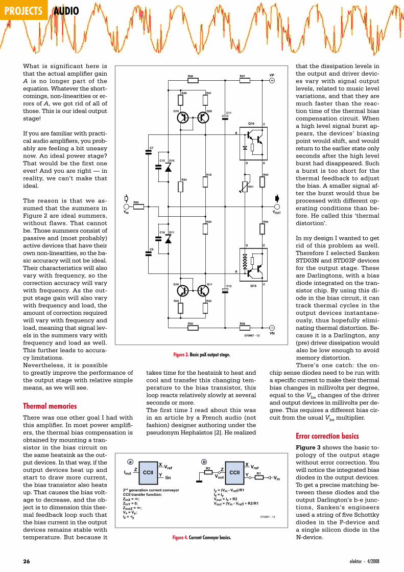
Error correction basicsFigure 3 shows the basic to-pology of the output stage without error correction. You will notice the integrated bias diodes in the output devices. To get a precise matching be-tween these diodes and the output Darlington’s b-e junc-tions, Sanken’s engineers used a string of five Schottky diodes in the P-device and a single silicon diode in the N-device.
takes time for the heatsink to heat and cool and transfer this changing tem-perature to the bias transistor, this loop reacts relatively slowly at several seconds or more.The first time I read about this was in an article by a French audio (not fashion) designer authoring under the pseudonym Hephaïstos [2]. He realized
RV1
Q11
Q20
R41
R43
Q18
Q19
R40
R42
R20
R19
R55
R54
C11
C12
R37
R44
R38R35
R36
D10
D11
C15
C16
VP
R60
C7
C8
VN
Q16
ED
C
B
Q15
ED
C
B
VOUTVIN
070987 - 13
VrefX
Z CCII YIout
2nd generation current conveyorCCII transfer function:ZinX = ∞;ZinY = 0;ZoutZ = ∞;
Iy = (Vin - Vref)/R1Iz = IyVout = Iz * R2Vout = (Vin - Vref) * R2/R1
Vx = Vy;Iz = -Iy
lin
070987 - 14
VrefX
Z CCII YVout Vin
R2R1
a b
Figure 3. Basic paX output stage.
Figure 4. Current Conveyor basics.
274/2008 - elektor
The datasheet specifies a bias cur-rent of 2.5 mA through the diodes, and this current is set by the current mirror formed by Q19-Q20 and Q18-Q11. The current is set with R44 and mirrored into the diodes. To keep this current stable, the supply voltage for the cur-rent mirrors is regulated by zener di-odes D10-D11 to 15 V. The bias for the zeners is coming from the main sup-ply via R36-R37 and R35-R38. To keep exactly that supply stable, the junc-tion between those resistors is boot-strapped from the output via C11-C12. The result is that with varying output signal levels, the zener diodes can al-ways provide a constant supply volt-age for the current mirrors.
The datasheet for the output devices also specifies a quiescent current of 40 mA through the output Darlingtons for best thermal tracking. Although the diodes track the changes in the Dar-lington Vbe quite well, the absolute val-ue of the diode threshold values varies from unit to unit. Thus, it is necessary to be able to adjust it, and that is the purpose of RV1. So, we should set RV1 for 40 mA through the output stage.OK, so now we have a nice and stable output stage, but we need to drive it with a signal. That is done through R60 to the junction of R19-R20. Suppose that the input signal goes positive: the junction of R19-R20 goes positive so there will be less current through R19. Since the current coming out of the collector of Q20 is fixed, there will be more current into the base of the Dar-lington and the output signal will also go positive, following the input signal. In this case there will also be more cur-rent through R20 so less from the base of the P-device.
This will work quite well for DC and low frequencies and nominal, resistive (8 ohms) loads, where the Darlingtons have a very high gain and the current mirrors are almost perfect. However, with increasing frequency and increas-ing load currents, the Darlingtons need more input current, so capacitors C7 and C8 are added to bypass R19-R20 so the input source can directly drive the output devices.
This output stage is quite simple, rea-sonably linear and satisfies the require-ment for accurate temperature track-ing of the instantaneous output device dissipation.The next step is to wrap error correc-
tion around it. Because the stage has no excess gain, you cannot use a glo-bal nfb loop around it. The nfb loop that normally includes the output stage of a feedback amplifier of course relies on the excess gain in the voltage amplify-ing stage to work its distortion-reduc-tion trick.
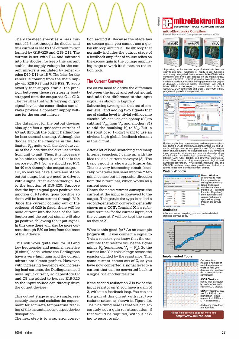
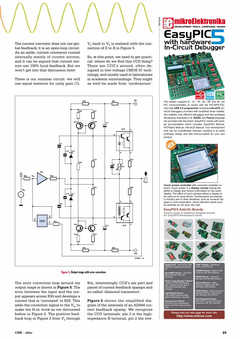
The Current ConveyorFor ec we need to derive the difference between the input and output signal, and add that difference to the input signal, as shown in Figure 2.Subtracting two signals that are of sim-ilar level, and adding two signals that are of similar level is trivial with opamp circuits. We can use one opamp (S2) to subtract Vout from Ve, and another (S1) to add the resulting Vc to Vin. But in the spirit of ec I didn’t want to use an obvious high global feedback element in this circuit.
After a lot of head scratching and many Internet searches, I came up with the idea to use a current conveyor [3]. The basic circuit is shown in Figure 4a. This is a very interesting circuit: basi-cally, whatever you send into the Y ter-minal comes out in opposite direction from the Z terminal, which works as a current source.Hence the name current conveyor: the current at the input is conveyed to the output. This particular type is called a second-generation conveyor, generally shown as a ‘CCII’. Terminal X is a refer-ence terminal for the current input, and the voltage at Y will be kept the same as that at X.
What is this good for? As an example (Figure 4b), if you connect a signal to Y via a resistor, you know that the cur-rent into that resistor will be the signal minus Vx (remember, VY = VX). So the current into Y is this voltage across the resistor divided by the resistance. That same current comes out of Z, so you have now converted a signal level to a current that can be converted back to a signal via another resistor.
If the second resistor on Z is twice the input resistor on Y, you have a gain of 2, without a feedback loop. You can set the gain of this circuit with just two resistor ratios, as shown in Figure 4b. The nice thing here is that we can ac-curately set a gain (or attenuation, if that would be required) without hav-ing to resort to nfb.
mikroElektronikaDEVELOPMENT TOOLS | COMPILERS | BOOKS
Please visit our web page for more infohttp://www.mikroe.com
mikroElektronika CompilersPascal, Basic and C Compilers for various MCUs
SupportingAan impressive range of microcontrollers, aneasy-to-useaIDE, hundreds of ready-to-use functionsand manyaintegrated toolsAmakes MikroElektronikacompilers one of the best choices on the market today.Besides mikroICD, mikroElektronika compilers offer astatistical module, simulator, bitmap generator for graph-ic displays, 7-segment display conversion tool, ASCIItable, HTML code export, communication tools forSD/MMC, UDP (Ethernet) and USB , EEPROM editor,programming mode management, etc.
Each compiler has many routines and examples such asEEPROM, FLASH and MMC, reading/writing SD and CFcards, writing character and graphics on LCDs, manipu-lation of push-buttons, 4x4 keyboard and PS/2 keyboardinput, generation of signals and sounds, character stringmanipulation, mathematical calculations, I2C, SPI,RS232, CAN, USB, RS485 and OneWire communica-tions, Manchester coding management, logical andnumerical conversion, PWM signals, interrupts, etc. TheCD-ROM contains many already-written and tested pro-grams to use with our development boards.Watch Window
Watch Windowallows you to moni-tor program itemsduring runtime simu-lation. It displaysvariables and con-troller's SFR (SpecialFunction Registers),their addresses andvalues. Values areupdated as you gothrough the simula-tion.
StatisticsAfter successful compiling, you can review detailed statistics on your code.
Implemented ToolsOur compilersinclude a number ofuseful implementedtools to help youdevelop your applica-tion more quickly andcomfortably.
ASCII Chart is ahandy tool, particular-ly useful when work-ing with LCD display.
USART Terminal is atool for RS232 com-munication - baudrate control, RTS andDTR commands...
And many more toolsare available.
Adver
tiseme
nt
projects audio
28 elektor - 4/2008
Error correction works by feeding back (part of) the output signal to the input of the amplifier. It has many similarities to a classical nega-tive feedback loop. But how is it different?
Two sides of the same medal. Figure 1a is the basic H.ec topol-ogy. You can identify two feedback loops: one positive feedback loop via Ve to Vc and back to Ve; and a negative feedback loop from the amplifier output to Vc. That particular arrangement makes H.ec so in-teresting. Let’s assume that the output stage ‘A’ is ideal and has a per-fect gain of 1. In that case, the correction signal at Vc is 0, because there is no difference between Ve and Vout. We could just throw away the whole error correction part. But if the gain A is just below 1, Vc is a negative signal which is subtracted from Vin and the effect is that Ve increases. This works as a positive feedback loop. In the case where the gain A would be larger than 1, the signal at Vc is a positive signal, which will be subtracted from Vin to decrease Ve. In this case, the system works as a negative feedback loop. So, what you see is a combined feedback loop that can act either as a positive or negative feedback loop, or not at all, depending on the error of the main amplifier block. It looks as if the phase and level of the loop adjusts itself as needed. The validity of treating a combined feedback loop by ‘summing’ the individual loop contributions has been established by several researchers in the past. Gerald Graeme, at the time analogue IC develop-ment manager of Burr-Brown, wrote several articles about it [1].
How does this differ from a ‘classical’ nega-tive feedback loop? We can take the two feedback loops in H.ec apart as in Figure 1b. Error correction can be seen as a classi-cal global nfb loop with a positive feedback loop embedded. For comparison, Figure 1c shows the global nfb topology for a uni-ty-gain amplifier.
Less complexity is better. In the classi-cal case, the high loop gain, necessary for negative feedback to reduce distortion, is obtained by means of a high-gain (ideally infinite-gain) forward amplifier block. In the case of H.ec, this high forward gain is ob-tained by a positive feedback loop, and the forward amplifier block can have any open-loop gain. To keep the task of a practical error correction circuit as small as possible (and therefore optimise the ec circuit linearity), the error signals should be minimal. For this, an open-loop gain equal to the required closed-loop gain is best. That means that with H.ec, similar results as with classical feedback can be reached with a much simpler amplifier. In the case of a unity gain amplifier, just an emit-ter follower would be sufficient, while in the classical case, even if we wanted a closed-loop gain of 1, we would still need a very high-gain amplifier block. If nothing else, this leads to the practical advantage
that the forward amplifier can be much simpler. Of course, there is no such thing as a free lunch (TANSTAFL): we have diverted some of the complexity to the two summers that must be precise circuits to make it all work. As always in audio engineering, the final advantage de-pends on how smart you are at implementing the various circuit parts.
Less gain is better. There is another advantage to H.ec. When a negative feedback amplifier clips, the feedback loop tries to make the output following the input by increasing the input signal more and more. But that output cannot increase beyond clipping, and as a re-sult the amplifier is overdriven. This can be quite drastic: consider an amp with a 1 V input signal and an open-loop gain of 60 dB (1000 times) and a closed-loop gain of 30 dB (30 times) that clips at 30 Vout.
If the output signal is 30 V, the effective input signal to the 60 dB gain amplifier (Vin – Vfeedback) is 30 V divided by the open-loop gain, or about 30 mV. If we overdrive this amplifier by doubling the input signal to 2 V, the feedback signal cannot increase due to clipping. So the effective input sig-nal to the 60 dB gain amplifier jumps from 30 mV to 1 V! (2 V input – 1 V feedback). The clipping will become very hard, and the output wave looks as a sine wave with the tops sheared off. There is a danger of heavy internal stage overdrive, and it is possible that it takes some time, after the clipping ends, until all internal stages are returned to their stable operation point. Many amplifiers will have measures to try to avoid these conditions but it does add to the complexity. With an H.ec amplifier, the mechanism is similar. The error cor-rection signal will increase and the input signal to the amplifier block is increased in an attempt to enable the output to follow the input. But now the amplifier block is a low-gain block, typically having a gain of only the closed-loop gain, for example only 30 dB, instead of the very high open-loop gain of 60 dB of the negative feedback amplifier. As a result, clipping and internal overdrive is not as hard. In my opinion, this is an important advantage, which is shared with valve amplifiers. Valved amps of mod-erate power output can sound quite pleas-ant, despite relatively high distortion fac-tors, which is to a large extend caused by their soft clipping characteristics. It is also
one of the reasons why very high power (300 W or more) solid state amplifiers sound better than 50 W amps with the same distortion: the high power amp clips far less than the low power amp, so the hard clipping, which can make the sound so harsh, is greatly reduced.
[1] “Generalized opamp model simplifies analysis of complex feed-back schemes” – Gerald G. Graeme, EDN, 15 April 1993, pp. 175.
How H.ec differs from Global Negative Feedback - or not.
Vin Ve
Vc
S1
S2
Vout
Gain ≈ 1
Vin Ve
S1
Vout
a
b
c
Gain = ∞
Vin Ve
S2
Vout
070987 - 19
S1
Gain ≈ 1
Figure 1a, top, is the basic error correction topology. In Figure 1b, middle, the two feedback loops are separated. The two figures are equivalent. Figure 1c, bottom, is a classical global nfb amplifier.
294/2008 - elektor
The current conveyer does not use glo-bal feedback; it is an open-loop circuit. As an aside, current conveyors consist internally mainly of current mirrors; and it can be argued that current mir-rors use 100% local feedback. But we won’t get into that discussion here!
There is our summer circuit: we will use equal resistors for unity gain (1).
The error correction loop around my output stage is shown in Figure 5. The error between the input and the out-put appears across R34 and develops a current that is ‘conveyed’ to R25. This adds the correction signal to the Vin to make the H.ec work as we discussed before in Figure 2. The positive feed-back loop in Figure 2 from Ve through
Vc back to Ve is realized with the con-nection of Z to X in Figure 5.
So, at this point, we need to get practi-cal: where do we find this CCII thing? There are CCII’s around, often de-signed in low-voltage CMOS IC tech-nology, and mostly used in laboratories in academic surroundings. They might as well be made from ‘unobtanium’.
But, interestingly, CCII’s are part and parcel of current feedback opamps and so-called ‘diamond transistors’.
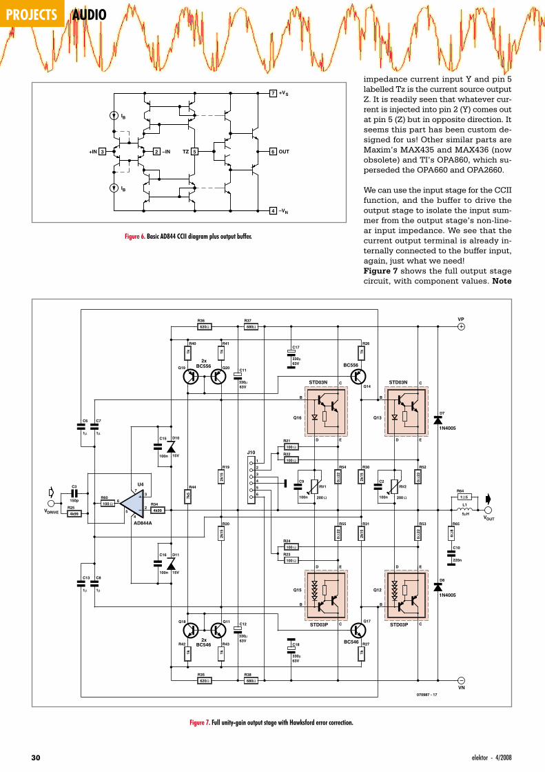
Figure 6 shows the simplified dia-gram of the internals of an AD844 cur-rent feedback opamp. We recognise the CCII terminals: pin 3 is the high-impedance X terminal, pin 2 the low-
mikroElektronikaDEVELOPMENT TOOLS | COMPILERS | BOOKS
The system supports 8-, 14-, 18-, 20-, 28- and 40- pinPIC microcontrollers (it comes with the PIC16F877A).Very fast USB 2.0 programmer including mikroICD (In-circuit Debugger) on-board with simplified driver installa-tion enables very efficient debugging and fast prototypedeveloping. Examples in C, BASIC and Pascal languageare provided with the board. EasyPIC5 comes with print-ed documentation which includes: EasyPIC5 Manual,PICFlash2 Manual, mikroICD Manual. Your developmenttime can be considerably reduced, resulting in an earlyprototype design and fast time-to-market for your endproduct.
CAN-1 Board - InterfacesCAN via MCP2551.
CANSPI Board - Makes CANnetwork with SPI interface.
RS485 Board - Connectsdevices into RS-485 network
Serial Ethernet - Make ethernet network with SPIInterface (ENC28J60).
IrDA2 Board - Irda2 serves aswireless RS232 communica-tion between two MCU’s.
Port Expander Board -MCP23S17 is the 16-bit portexpander with SPI interface.
Digital POT - MCP41010 SPIInterfaced digital potentiome-ter.
SmartMP3 Board - VS1001kMP3 decoder with SPIInterface.
Serial 7-seg Display 2 Board- MAX7219 SPI Interfaced,LED Display Drivers with 8Common-Cathode LEDDisplays
LightToFreq Board -TSL230BR programmablelight-to-frequency converter.
EasyConnect Board -Connects your peripheralseasily and fast using connec-tors.
EasyPIC5 Add-On BoardsVarious range of additional daughter-boards for EasyPIC5 development board
Please visit our web page for more infohttp://www.mikroe.com
Touch screen controller with connector available on-board. Touch screen is a display overlay having theability to display and receive information on the samedisplay. The effect of such overlays allows a display tobe used as an input device. Touchscreens are popularin industry and in other situations, such as museum dis-plays or room automation, where standard inputs suchas switches do not work very well.
Adver
tiseme
nt
RV1C9
Q11
Q20
R41
R43
Q18
Q19
R40
R42
R20
R19
R55
R54
C11
C12
R37
R44
R38R35
R36
D10
D11
C15
C16
VP
R60
C7
C8
R25
VN
070987 - 15
Q16
ED
C
B
Q15
ED
C
B
U4
R34
VOUT
Ve
VIN
CCIIZ
X
Y
Figure 5. Output stage with error correction.
projects audio
30 elektor - 4/2008
impedance current input Y and pin 5 labelled Tz is the current source output Z. It is readily seen that whatever cur-rent is injected into pin 2 (Y) comes out at pin 5 (Z) but in opposite direction. It seems this part has been custom de-signed for us! Other similar parts are Maxim’s MAX435 and MAX436 (now obsolete) and TI’s OPA860, which su-perseded the OPA660 and OPA2660.
We can use the input stage for the CCII function, and the buffer to drive the output stage to isolate the input sum-mer from the output stage’s non-line-ar input impedance. We see that the current output terminal is already in-ternally connected to the buffer input, again, just what we need!Figure 7 shows the full output stage circuit, with component values. Note
+IN OUT3 2 5 6
7
4
–IN
+VS
–VN
TZ
IB
IB
Figure 6. Basic AD844 CCII diagram plus output buffer.
R52
0Ω
22
R53
0Ω
22D7
1N4005
D8
1N4005
200 Ω
RV2C2
100n
R54
0Ω
22
R55
0Ω
22
200 Ω
RV1C9
100n
1
2
3
4
5
6
J10
R21
100 Ω
R22
100 Ω
R24
100 Ω
R23
100 Ω
R64
1Ω5
L1
5µH
R65
6Ω
8
C10
220n
R30
2k15
R31
2k15
Q17
BC546
Q14
BC556
R26
1k
R27
1k
Q11
Q20BC556
R41
1k
R43
1k
Q18
BC546
Q19
R40
1k
R42
1k
2x
2x
R20
2k15
R19
2k15
C11
330µ63V
C12
330µ63V
R37
680Ω
R44
7k5
R38
680ΩR35
620Ω
R36
620Ω
D10
15V
D11
15V
C15
100n
C16
100n
C18
330µ63V
C17
330µ63V
VP
R34
4k99
AD844A
U4
2
3
6
7
45
R60
100 Ω
C7
1µ
C8
1µ
C6
1µ
C13
1µ
R25
4k99
C3
150p
VN070987 - 17
Q12
STD03P
ED
C
B
Q15
STD03P
ED
C
B
Q13
STD03N
ED
C
B
Q16
STD03N
ED
C
B
VDRIVEVOUT
Figure 7. Full unity-gain output stage with Hawksford error correction.
314/2008 - elektor
that the amplifier input is at pin 5 of the AD844, not at pin 2 or pin 3 as we would expect in a classical opamp circuit. This is NOT an opamp circuit, but I’m sure a lot of people will be con-fused by this...
Putting it all togetherThis output stage has two pairs of output devices. The design goal was
100 watts in 8 Ω and 200 watts in 4 Ω. For a pure resistive load, one pair of de-vices would have been sufficient. How-ever, speakers are not purely resistive; depending on the signal frequency they can act capacitive or inductive, especially if there is a complex cross-over filter. This leads to phase shifts between the output voltage and output current, so you can get the situation that the output voltage is negative,
mikroElektronikaDEVELOPMENT TOOLS | COMPILERS | BOOKS
Please visit our web page for more infohttp://www.mikroe.com
Microchip's ENC28J60 is a28-pin, 10BASE-T standalone Ethernet Controllerwith on board MAC & PHY,8 Kbytes of Buffer RAMand an SPI serial interface.
Extra Development Add-On BoardsLarge range of additional daughter-boards for various development boards
Add MP3 to your prototypewith VS1001k MPEG audiolayer 3 decoder with SPIInterface. Low VoltageAudio Power Amplifiersand Voltage LevelSelection - 5V or 3.3V.
The ADXL330 is a small,thin, low power, complete3-axis accelerometer withsignal conditioned voltageoutputs, all on a singlemonolithic IC.
MCP2120 encodes anasynchronous serial datastream, converting eachdata bit to the correspon-ding Infrared (IR) formattedpulse.
Connect multiple devicesinto RS-485 network usingLTC485 is a low power dif-ferential bus/line transceiv-er. It also meets therequirements of RS422.
MAX7219 SPI Interfaced,LED Display Drivers with 8Common-Cathode LEDDisplays on-board.Connects via IDC10 con-nector on-board.
Add light to frequency con-verter to your prototypewith TSL230BR program-mable light-to-frequencyconverter on-board.
The MCP4921 is a generalpurpose DAC intended tobe used in applicationswhere a precision, low-power DAC with moderatebandwidth is required.
12-bit analog-to-digital con-verter (ADC) MCP3204with SPI, operational ampli-fier MCP6024 ,4 inputs,4.096V voltage reference.
ULN2804 - High-currentDarlington arrays are ideal-ly suited for interfacingbetween low-level logic cir-cuitry and multiple periph-eral power loads.
Adver
tiseme
nt
0.001
0.2
0.002
0.005
0.01
0.02
0.05
0.1
%
20 20k50 100 200 500 1k 2k 5k 10k
Hz
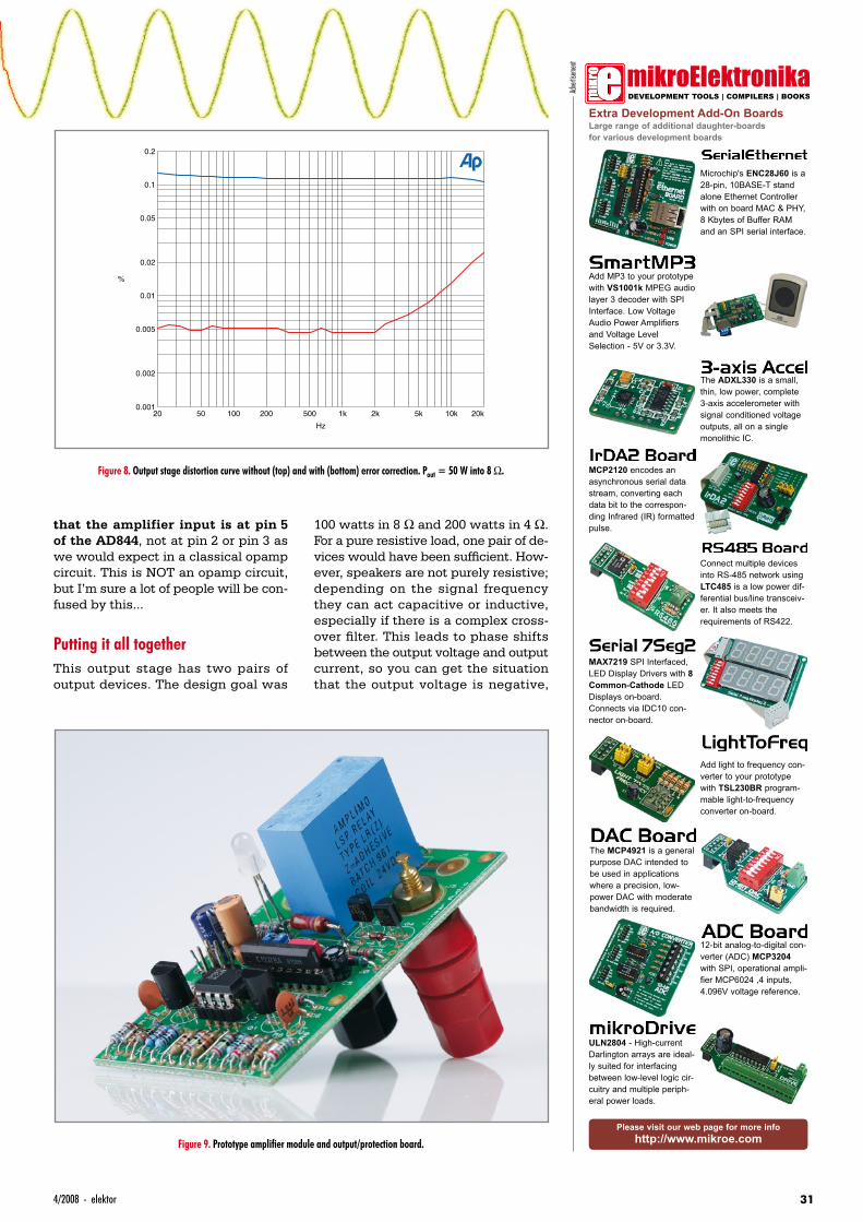
Figure 8. Output stage distortion curve without (top) and with (bottom) error correction. Pout = 50 W into 8 Ω.
Figure 9. Prototype amplifier module and output/protection board.
projects audio
32 elektor - 4/2008
but that the current is coming from the positive side (the N-device). The N-device will have a quite large Vce, and the current it is allowed to source is much smaller with a large Vce than what you would think from the allow-able dissipation.Further details about the safe opera-tion area of the output devices will be given in a separate article next month. Anyway, because of the dual output devices, there is also an additional cur-rent source to bias the thermal track-ing diodes, as well as an extra bias ad-just trimmer.
There are a few extra components in the circuit which we haven’t men-tioned before.R60 is a small resistor in series with the AD844 buffer output stage. A large part of the output drive goes via the two capacitors C2 and C4 to bypass the current mirrors. R60 isolates the buffer output from capacitive loads en-suring stability.Another capacitor, C3, is placed across R25. As the frequency increases, the loop through the output stage as well
output stage can perfectly stand on its own when driven by a suitable voltage amplifier (Vas) stage. So, let’s take a break here; we’ll attack that Vas, and the power supply, in the next instal-ment and develop a full-fledged, high quality audio power amp. Stay tuned.
(070987-I)
Literature and note[1] Hawksford, M.J., ‘Distortion correction in audio power amplifiers’, JAES, Vol. 29, No.1/2. pp. 27-30, Jan/Feb 1981.
[2] Hephaïstos, ‘Thermal Distortion – it exists,
I’ve seen it’, L’Audiophile, no. 32, May 1984. (Ed.: Hephaistos was the Greek god of fire, metalworking, stonemasonry and the art of sculpture)
[3] In the early 90’s, an IC designer, Doug Wadsworth, designed a current conveyor for audio on his own money (PA630). The chip, the ‘Swift Current’ chip, eventually found its way into Wadia DACs. It is no longer availa-ble for other parties, but I had bought some from him and knew they were a well kept se-cret for hi-end audio.
as the current conveyor will exhibit phase shift. In a ‘classical’ feedback amplifier, if the phase shift becomes too large, it will turn the nfb into pfb which, as we all know, will lead to in-stability and even oscillations. In H.ec this is also the case of course (it shares many attributes with a feedback am-plifier), so we need to roll off the loop gain for higher frequencies, just as in a classical nfb amplifier. C3 does just that by decreasing the effective correc-tion impedance (R25//C3) with increas-ing frequency.Also remember that this stage needs
to be driven from a low impedance source, because the source output im-pedance forms part of the ec scaling resistor R25.Finally, there is the 6-pin connector J10 and some associated resistors. This is the connection to the protection board which we will discuss separately. It provides the Vce and Ic related infor-mation of the output devices to the pro-tection circuitry.This output stage is pretty linear as at-tested by the curves in Figure 8. The
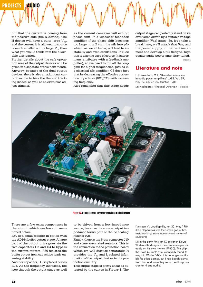
Figuur 10. De opgebouwde versterker-module op z’n koellichaam.