proper decoupling poor decoupling - amazon s3 · series resonance in decoupling capacitors this is...
TRANSCRIPT
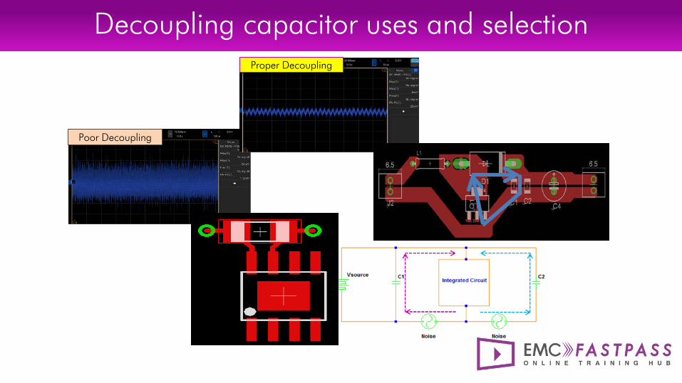
Decoupling capacitor uses and selection
Poor Decoupling
Proper Decoupling
Covered in this topic:
• 3 different uses of decoupling capacitors • Why we need decoupling capacitors • Power supply rail with poor and proper decoupling • Ideal versus actual decoupling network • Series resonance in decoupling capacitors • How much decoupling capacitance to use? • Mathematical approach to decoupling capacitor selection • Effect of decoupling on radiated emission • X2Y capacitors benefits and uses
Introduction
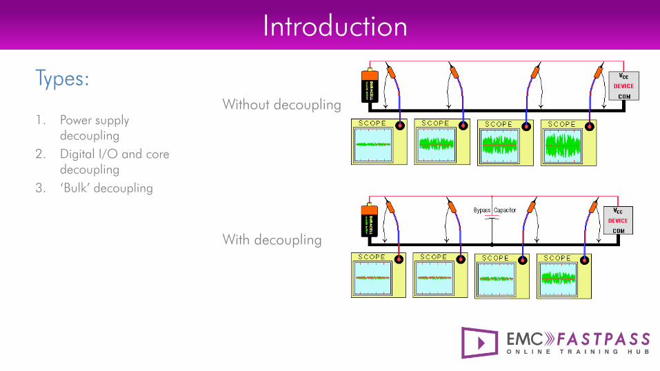
Types:
1. Power supply decoupling
2. Digital I/O and core decoupling
3. ‘Bulk’ decoupling
Introduction
Without decoupling
With decoupling
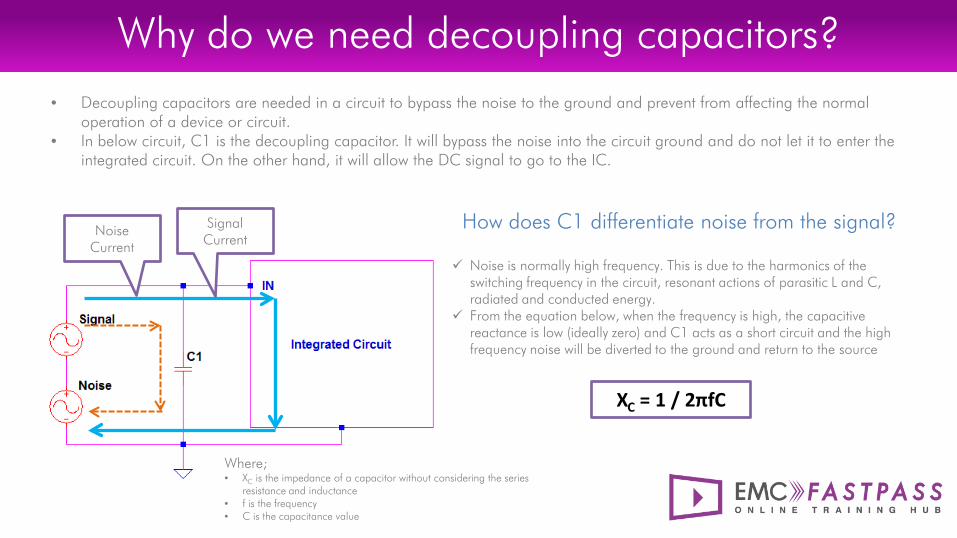
Why do we need decoupling capacitors? • Decoupling capacitors are needed in a circuit to bypass the noise to the ground and prevent from affecting the normal
operation of a device or circuit. • In below circuit, C1 is the decoupling capacitor. It will bypass the noise into the circuit ground and do not let it to enter the
integrated circuit. On the other hand, it will allow the DC signal to go to the IC.
XC = 1 / 2πfC
Where; • XC is the impedance of a capacitor without considering the series
resistance and inductance • f is the frequency • C is the capacitance value
Noise Current
Signal Current
How does C1 differentiate noise from the signal?
Noise is normally high frequency. This is due to the harmonics of the switching frequency in the circuit, resonant actions of parasitic L and C, radiated and conducted energy.
From the equation below, when the frequency is high, the capacitive reactance is low (ideally zero) and C1 acts as a short circuit and the high frequency noise will be diverted to the ground and return to the source
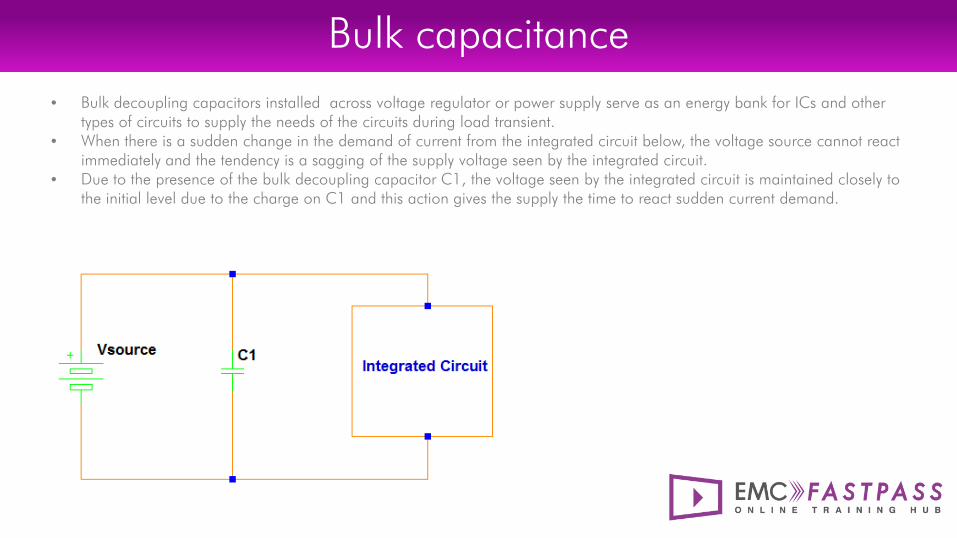
Bulk capacitance • Bulk decoupling capacitors installed across voltage regulator or power supply serve as an energy bank for ICs and other
types of circuits to supply the needs of the circuits during load transient. • When there is a sudden change in the demand of current from the integrated circuit below, the voltage source cannot react
immediately and the tendency is a sagging of the supply voltage seen by the integrated circuit. • Due to the presence of the bulk decoupling capacitor C1, the voltage seen by the integrated circuit is maintained closely to
the initial level due to the charge on C1 and this action gives the supply the time to react sudden current demand.
Digital IC decoupling
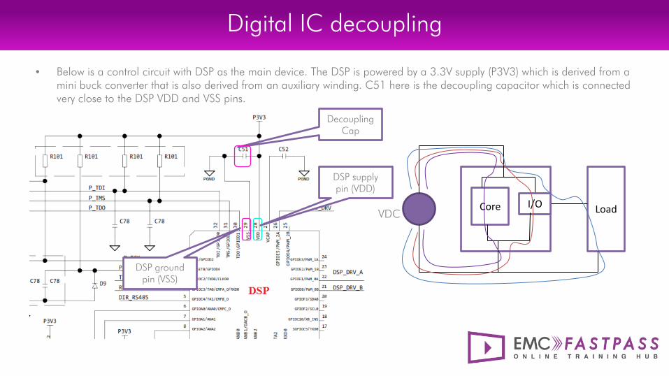
• Below is a control circuit with DSP as the main device. The DSP is powered by a 3.3V supply (P3V3) which is derived from a mini buck converter that is also derived from an auxiliary winding. C51 here is the decoupling capacitor which is connected very close to the DSP VDD and VSS pins.
Decoupling Cap
DSP ground pin (VSS)
DSP supply pin (VDD)
Core Load I/O VDC
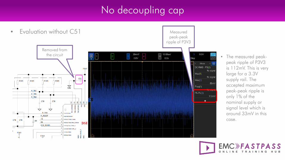
No decoupling cap
• Evaluation without C51
Removed from the circuit
Measured peak-peak
ripple of P3V3
• The measured peak-peak ripple of P3V3 is 112mV. This is very large for a 3.3V supply rail. The accepted maximum peak-peak ripple is only 1% of the nominal supply or signal level which is around 33mV in this case.
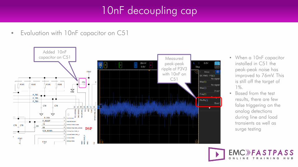
10nF decoupling cap
• Evaluation with 10nF capacitor on C51
Added 10nF capacitor on C51 • When a 10nF capacitor
installed in C51 the peak-peak noise has improved to 76mV. This is still off the target of 1%.
• Based from the test results, there are few false triggering on the analog detections during line and load transients as well as surge testing
Measured peak-peak
ripple of P3V3 with 10nF on
C51
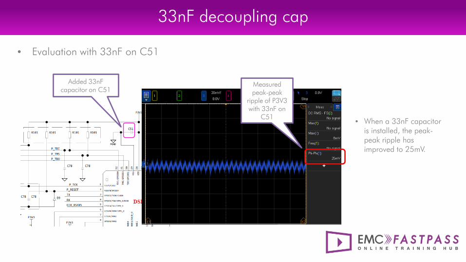
33nF decoupling cap
• Evaluation with 33nF on C51
Added 33nF capacitor on C51
• When a 33nF capacitor is installed, the peak-peak ripple has improved to 25mV.
Measured peak-peak
ripple of P3V3 with 33nF on
C51
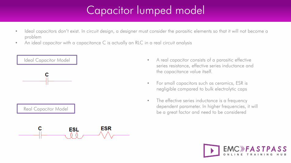
Capacitor lumped model
• Ideal capacitors don’t exist. In circuit design, a designer must consider the parasitic elements so that it will not become a problem
• An ideal capacitor with a capacitance C is actually an RLC in a real circuit analysis
• A real capacitor consists of a parasitic effective series resistance, effective series inductance and the capacitance value itself.
• For small capacitors such as ceramics, ESR is negligible compared to bulk electrolytic caps
• The effective series inductance is a frequency dependent parameter. In higher frequencies, it will be a great factor and need to be considered
Ideal Capacitor Model
Real Capacitor Model
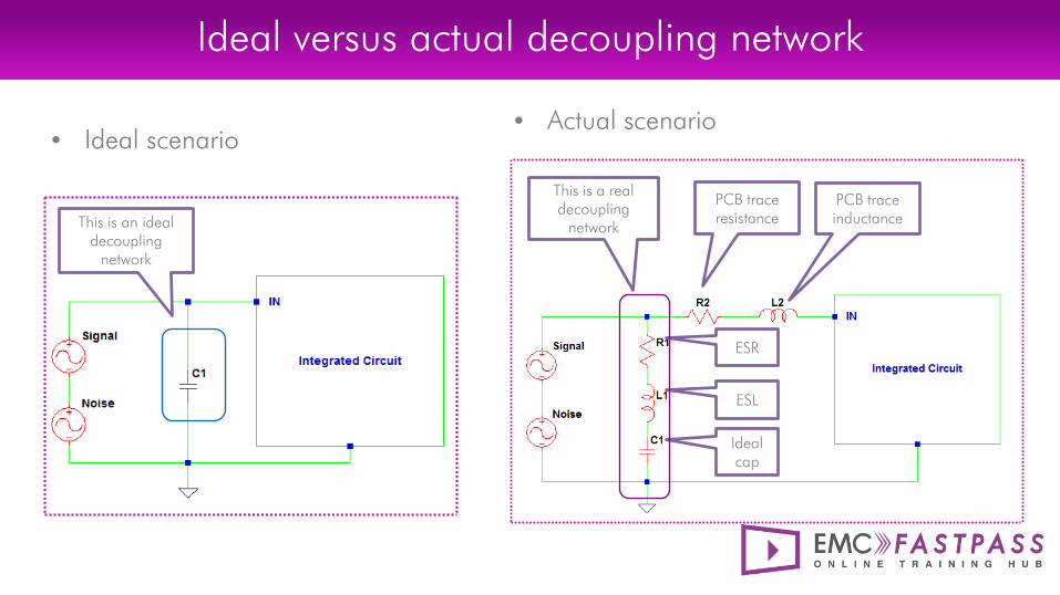
This is a real decoupling
network
ESR
ESL
Ideal cap
PCB trace resistance
Ideal versus actual decoupling network
This is an ideal decoupling
network
PCB trace inductance
• Ideal scenario • Actual scenario
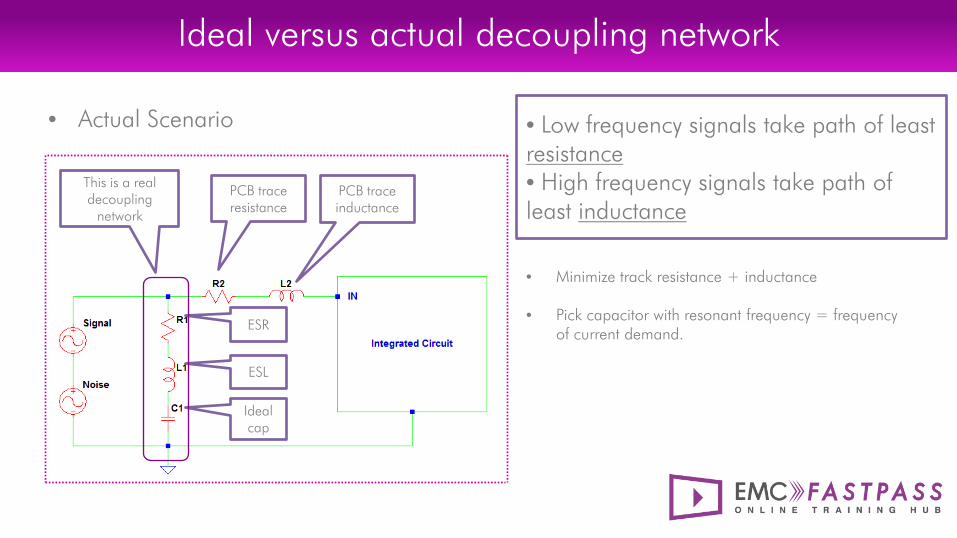
This is a real decoupling
network
ESR
ESL
Ideal cap
PCB trace resistance
Ideal versus actual decoupling network
PCB trace inductance
• Actual Scenario
• Minimize track resistance + inductance
• Pick capacitor with resonant frequency = frequency of current demand.
• Low frequency signals take path of least resistance • High frequency signals take path of least inductance
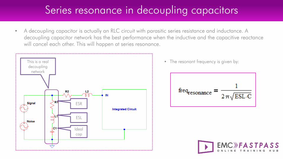
Series resonance in decoupling capacitors
This is a real decoupling
network
ESR
ESL
Ideal cap
• A decoupling capacitor is actually an RLC circuit with parasitic series resistance and inductance. A decoupling capacitor network has the best performance when the inductive and the capacitive reactance will cancel each other. This will happen at series resonance.
• The resonant frequency is given by:
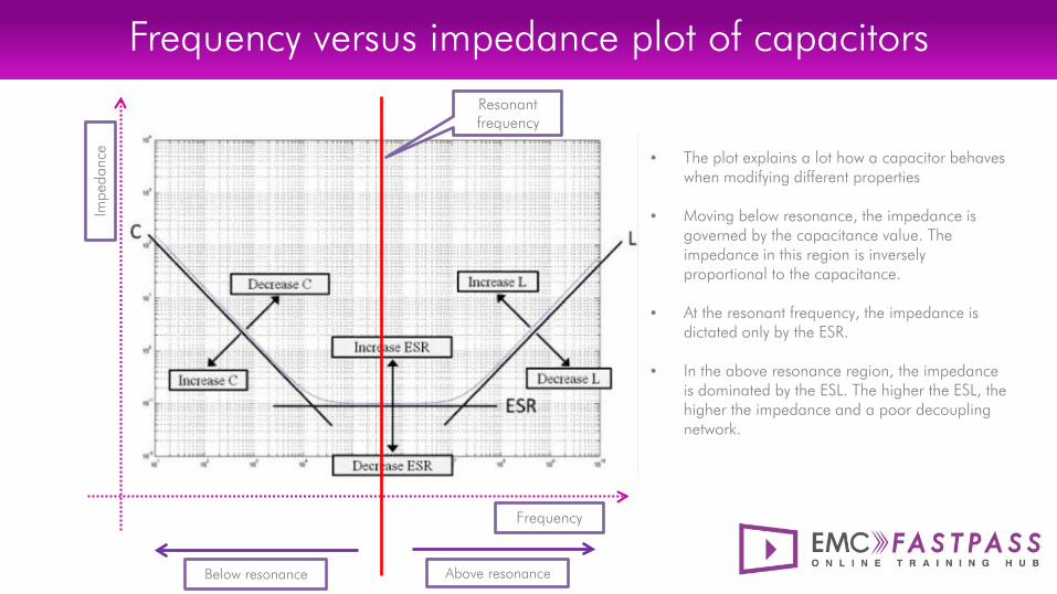
Frequency versus impedance plot of capacitors Im
peda
nce
Frequency
Resonant frequency
Below resonance Above resonance
• The plot explains a lot how a capacitor behaves when modifying different properties
• Moving below resonance, the impedance is
governed by the capacitance value. The impedance in this region is inversely proportional to the capacitance.
• At the resonant frequency, the impedance is dictated only by the ESR.
• In the above resonance region, the impedance is dominated by the ESL. The higher the ESL, the higher the impedance and a poor decoupling network.
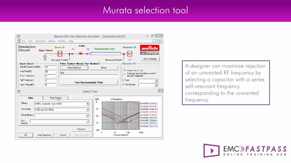
Murata selection tool
A designer can maximize rejection of an unwanted RF frequency by selecting a capacitor with a series self-resonant frequency corresponding to the unwanted frequency.
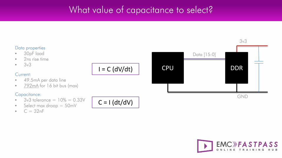
What value of capacitance to select?
Data properties • 30pF load • 2ns rise time • 3v3 DDR CPU I = C (dV/dt)
Data [15:0]
3v3
GND
Current: • 49.5mA per data line • 792mA for 16 bit bus (max)
Capacitance: • 3v3 tolerance = 10% = 0.33V • Select max droop = 50mV • C = 32nF
C = I (dt/dV)
Effect of decoupling on radiated emission
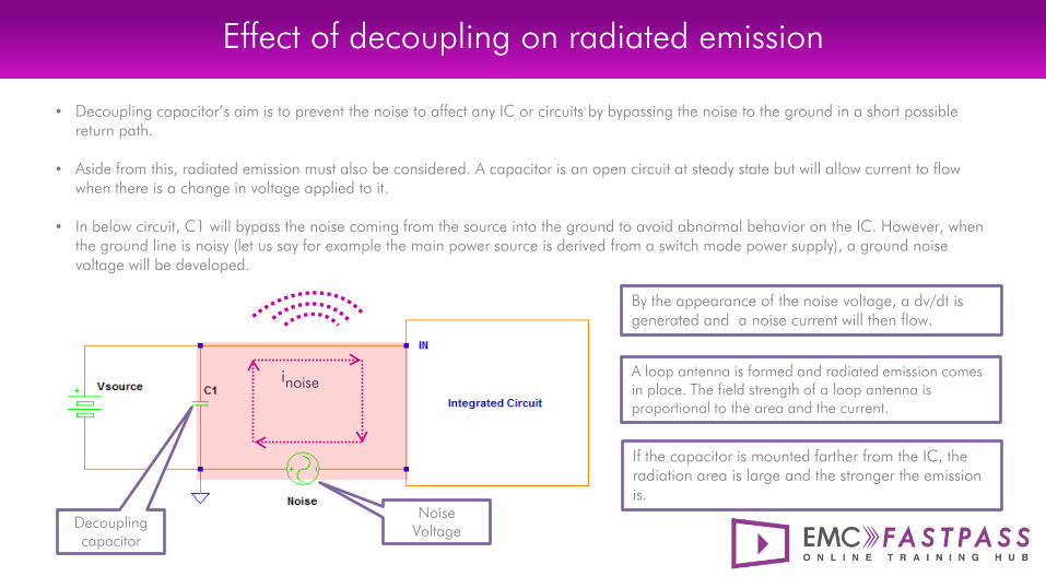
• Decoupling capacitor’s aim is to prevent the noise to affect any IC or circuits by bypassing the noise to the ground in a short possible return path.
• Aside from this, radiated emission must also be considered. A capacitor is an open circuit at steady state but will allow current to flow when there is a change in voltage applied to it.
• In below circuit, C1 will bypass the noise coming from the source into the ground to avoid abnormal behavior on the IC. However, when the ground line is noisy (let us say for example the main power source is derived from a switch mode power supply), a ground noise voltage will be developed.
If the capacitor is mounted farther from the IC, the radiation area is large and the stronger the emission is.
inoise
Noise Voltage
By the appearance of the noise voltage, a dv/dt is generated and a noise current will then flow.
A loop antenna is formed and radiated emission comes in place. The field strength of a loop antenna is proportional to the area and the current.
Decoupling capacitor
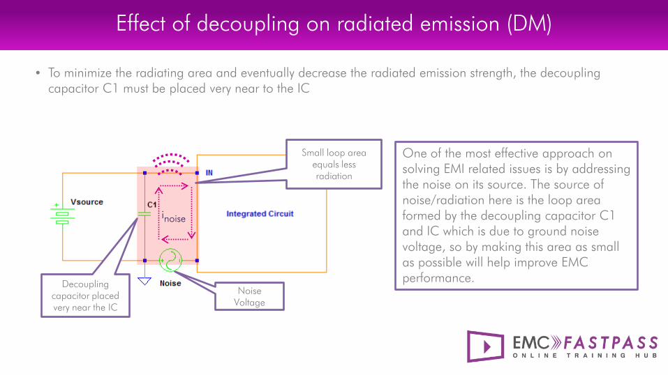
Effect of decoupling on radiated emission (DM)
One of the most effective approach on solving EMI related issues is by addressing the noise on its source. The source of noise/radiation here is the loop area formed by the decoupling capacitor C1 and IC which is due to ground noise voltage, so by making this area as small as possible will help improve EMC performance.
inoise
Noise Voltage
• To minimize the radiating area and eventually decrease the radiated emission strength, the decoupling capacitor C1 must be placed very near to the IC
Decoupling capacitor placed very near the IC
Small loop area equals less radiation
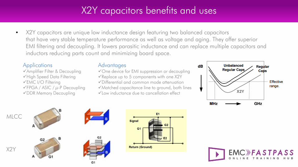
X2Y capacitors benefits and uses
Applications Amplifier Filter & Decoupling High Speed Data Filtering EMC I/O Filtering FPGA / ASIC / μ-P Decoupling DDR Memory Decoupling
• X2Y capacitors are unique low inductance design featuring two balanced capacitors that have very stable temperature performance as well as voltage and aging. They offer superior EMI filtering and decoupling. It lowers parasitic inductance and can replace multiple capacitors and inductors reducing parts count and minimizing board space.
Advantages One device for EMI suppression or decoupling Replace up to 5 components with one X2Y Differential and common mode attenuation Matched capacitance line to ground, both lines Low inductance due to cancellation effect
MLCC
X2Y
Summary
Summary:
• 3 different uses of decoupling capacitors • Why we need decoupling capacitors • Power supply rail with poor and proper decoupling • Ideal versus actual decoupling network • Series resonance in decoupling capacitors • How much decoupling capacitance to use? • Mathematical approach to decoupling capacitor selection • Effect of decoupling on radiated emission • X2Y capacitors benefits and uses