proposal for a silicon vertex tracker (vtx) for the...
TRANSCRIPT

PROPOSAL for a Silicon Vertex Tracker
(VTX) for the PHENIX Experiment

ii
Proposal for a Silicon Vertex Tracker (VTX) for the PHENIX Experiment
M. Baker, R. Nouicer, R. Pak, A. Sukhanov, P. Steinberg
Brookhaven National Laboratory, Chemistry Department, Upton, NY 11973-5000, USA
Z. Li Brookhaven National Laboratory, Instrumentation Division, Upton, NY 11973-5000, USA
J.S. Haggerty, J.T. Mitchell, C.L. Woody
Brookhaven National Laboratory, Physics Department, Upton, NY 11973-5000, USA
A.D. Frawley Florida State University, Tallahassee, FL 32306, USA
J. Crandall, J.C. Hill, J.G. Lajoie, C.A. Ogilvie, A. Lebedev, H. Pei, J. Rak, G.Skank,
S. Skutnik, G. Sleege, G. Tuttle Iowa State University, Ames, IA 56011, USA
M. Tanaka
High Energy Accelerator Research Organization (KEK), Tsukuba, Ibaraki 305-0801, Japan.
N. Saito, M. Togawa, M. Wagner Kyoto University, Kyoto 606, Japan
H.W. van Hecke, G.J. Kunde, D.M. Lee, M. J. Leitch, P.L. McGaughey, W.E. Sondheim
Los Alamos National Laboratory, Los Alamos, NM 87545, USA
T. Kawasaki, K. Fujiwara Niigata University, Niigata 950-2181, Japan
T.C. Awes, M. Bobrek, C.L. Britton, W.L. Bryan, K.N. Castleberry, V. Cianciolo,
Y.V. Efremenko, K.F. Read, D.O. Silvermyr, P.W. Stankus, A.L. Wintenberg, G.R. Young Oak Ridge National Laboratory, Oak Ridge, TN 37831, USA
Y. Akiba, H. En’yo, Y. Goto, J.M. Heuser, H. Kano, H. Ohnishi, V. Rykov, A. Taketani,
K.Tanida, J. Tojo RIKEN (The Institute of Physical and Chemical Research,) Wako, Saitama 351-0198, Japan
J. Asai, T. Tabaru
RIKEN BNL Research Center, Brookhaven National Laboratory, Upton, NY11973-5000, USA
S. Abeytunge, R. Averbeck, K. Boyle, A. Deshpande , A. Dion, A. Drees, T.K. Hemmick,
B.V. Jacak, C. Pancake, V.S. Pantuev, H.W. Themann, D. Walker Stony Brook University, Department of Physics and Astronomy, Stony Brook, NY 11794, USA
B. Bassalleck, D.E. Fields, M. Malik
University of New Mexico, Albuquerque, NM, USA

i
1. EXECUTIVE SUMMARY....................................................................................................... 1
2. PHYSICS OVERVIEW ............................................................................................................ 4 2.1 PROBES OF EARLY, HIGHEST ENERGY-DENSITY STAGE OF HEAVY-ION REACTIONS........ 4 POTENTIAL ENHANCEMENT OF OPEN CHARM PRODUCTION ............................................................ 5 OPEN BEAUTY PRODUCTION ........................................................................................................... 6 RATIO OF CHARM AND BEAUTY PRODUCTION AND ITS CENTRALITY DEPENDENCE........................ 7 ENERGY-LOSS OF HEAVY-QUARKS .................................................................................................. 7 OPEN CHARM REFERENCE TO J/ψ SUPPRESSION AND ENHANCEMENT............................................. 9 OPEN BEAUTY AND J/ψ SUPPRESSION ........................................................................................... 10 THERMAL DI-LEPTON AND OPEN CHARM....................................................................................... 11 HIGH PT PHENOMENA WITH LIGHT FLAVOR IN 10 – 15 GEV/C IN PT.............................................. 12 MEASUREMENT OF UPSILON STATES............................................................................................. 12 2.2 DETERMINATION OF SPIN STRUCTURE OF NUCLEON. .......................................................... 12 EXPLORING THE SPIN STRUCTURE OF THE NUCLEON: THE PAST ................................................... 12 GLUON POLARIZATION MEASUREMENT AT RHIC: ........................................................................ 13 THE ROLE OF SILICON VERTEX DETECTOR: .................................................................................. 14 THE HEAVY QUARK PHYSICS (OPEN CHARM AND BEAUTY PRODUCTION)..................................... 15 DIRECT PHOTON + JET MEASUREMENT: ........................................................................................ 16 OTHER ADVANTAGES OF THE SILICON VERTEX DETECTOR:......................................................... 17 2.3 EXPLORATION OF THE NUCLEON STRUCTURE IN NUCLEI ................................................... 18
3. PHYSICS MEASUREMENTS WITH THE VTX DETECTOR ........................................ 23 3.1 DESIGN CONSIDERATIONS AND THE VTX DETECTOR GEOMETRY..................................... 23 DESIGN CONSIDERATIONS............................................................................................................. 23 VTX DETECTOR GEOMETRY.......................................................................................................... 24 DETECTOR OCCUPANCY................................................................................................................ 25 CENTRAL TRACK – VTX MATCHING............................................................................................. 26 3.2 OPEN CHARM AND BEAUTY MEASUREMENT ....................................................................... 29 OPEN CHARM MEASUREMENT FROM SEMI-LEPTONIC DECAY ....................................................... 29 DIRECT MEASUREMENT OF D0 K-π+ AT HIGH PT......................................................................... 31 OPEN BEAUTY MEASUREMENT ..................................................................................................... 34 3.3 PHOTON AND JETS MEASUREMENT IN POLARIZED P+P ....................................................... 36 3.4 IMPROVED MOMENTUM RESOLUTION AND PT RESOLUTION ............................................... 39 3.5 FIRST LEVEL TRIGGER CAPABILITIES................................................................................... 41 3.6 EVENT RATE ESTIMATES........................................................................................................ 43
4. VTX DETECTOR SYSTEM.................................................................................................. 48 4.1 OVERVIEW .............................................................................................................................. 48 4.2 HYBRID PIXELS....................................................................................................................... 50 SENSOR .......................................................................................................................................... 51 READOUT CHIP............................................................................................................................... 53 INTERCONNECTION OF SENSOR AND READOUT CHIP (“BUMP BONDING”)................................... 55 PILOT MODULE............................................................................................................................... 57 READOUT BUS ............................................................................................................................... 59 FRONT END MODULES................................................................................................................... 61 PIXEL DETECTORS OPERATING IN THE NA60 EXPERIMENT:.......................................................... 62

ii
4.3 SILICON STRIP DETECTOR .................................................................................................... 64 STRIP SENSORS .............................................................................................................................. 64 LABORATORY TESTS OF THE STRIP SENSORS................................................................................. 65 BEAM TEST OF THE FIRST GENERATION SENSOR PROTO-TYPE ...................................................... 67 THE SECOND PROTOTYPE SENSOR AND TESTS WITH SVX4 READOUT CHIP................................ 70 NEW SENSOR DESIGN.................................................................................................................... 70 SENSOR PRE-PRODUCTION............................................................................................................. 72 SVX4 READOUT CHIP .................................................................................................................... 72 SENSOR READOUT CARD (ROC) / READOUT BUS......................................................................... 73 PILOT MODULE.............................................................................................................................. 76 FRONT-END MODULE.................................................................................................................... 77 ROC THICKNESS............................................................................................................................ 78 ZERO SUPPRESSION ....................................................................................................................... 78 SI STRIP PRODUCTION/TESTING/ASSEMBLY SCHEDULE ................................................................. 79 4.4 MECHANICAL STRUCTURE AND COOLING ........................................................................... 83 DESIGN CRITERIA .......................................................................................................................... 84 STRUCTURAL SUPPORT.................................................................................................................. 85 DETECTOR LADDERS AND COOLING ............................................................................................. 86 RADIATION LENGTH ...................................................................................................................... 89 4.5 DETECTOR INTEGRATION INTO PHENIX ............................................................................ 89 VTX DETECTOR ASSEMBLY........................................................................................................... 89 ERROR BUDGET ............................................................................................................................. 89 LADDER ASSEMBLY - PIXELS......................................................................................................... 90 LADDER ASSEMBLY – STRIPS ........................................................................................................ 90 HALF DETECTOR ASSEMBLY.......................................................................................................... 91 INTEGRATION INTO PHENIX......................................................................................................... 91 DAQ .............................................................................................................................................. 93
5. R&D.......................................................................................................................................... 94
6. PROJECT MANAGEMENT AND RESPONSIBILITIES ................................................. 97 6.1 PROJECT BACKGROUND......................................................................................................... 97 6.2 THE MANAGEMENT PLAN FOR THE VTX.............................................................................. 99 PHENIX MANAGEMENT STRUCTURE ............................................................................................ 99 PHENIX SUBSYSTEM LEADERSHIP.............................................................................................. 100 ROLE OF BNL .............................................................................................................................. 101 SPECIFICATION OF DELIVERABLES .............................................................................................. 102 6.3 MANPOWER FOR TASKS....................................................................................................... 103 6.4 INSTITUTIONAL INVOLVEMENT........................................................................................... 104 BROOKHAVEN NATIONAL LABORATORY, CHEMISTRY DEPARTMENT (BNL CHEM)................ 105 BROOKHAVEN NATIONAL LABORATORY, INSTRUMENTATION DIVISION (BNL ID) .................. 105 BROOKHAVEN NATIONAL LABORATORY, PHYSICS DEPARTMENT (BNL PHY)......................... 106 IOWA STATE UNIVERSITY (ISU).................................................................................................. 106 KYOTO UNIVERSITY (KYOTO)..................................................................................................... 107 LOS ALAMOS NATIONAL LABORATORY (LANL) ....................................................................... 107 UNIVERSITY OF NEW MEXICO, ALBUQUERQUE (UNM) ............................................................. 107 OAK RIDGE NATIONAL LABORATORY (ORNL) .......................................................................... 108 RIKEN INSTITUTE (RIKEN) AND RBRC .................................................................................... 108 STONY BROOK UNIVERSITY, PHYSICS DEPARTMENT (SBU)...................................................... 109 6.5 FOREIGN CONTRIBUTIONS................................................................................................... 109

iii
7 BUDGET AND SCHEDULE ............................................................................................. 111 7.1 TOTAL ESTIMATED COST (TEC) ......................................................................................... 111 FISCAL RESPONSIBILITIES ........................................................................................................... 111 CONTINGENCY ANALYSIS ........................................................................................................... 111 OVERHEAD ESTIMATE ................................................................................................................. 111 BUDGET ....................................................................................................................................... 112 7.2 SCHEDULE............................................................................................................................. 115
APPENDIX A ENDCAP EXTENSION.............................................................................. 118 INTRODUCTION........................................................................................................................... 118 A.1 GOALS OF THE ENDCAP UPGRADE..................................................................................... 120 A.1.1 SPIN STRUCTURE OF THE NUCLEON .................................................................................. 120 A.1.2 EXPLORATION OF GLUON STRUCTURE IN NUCLEI ............................................................ 121 A.1.3 PROBES OF EARLY, HIGHEST ENERGY-DENSITY STAGE OF HEAVY-ION REACTIONS....... 122 ENERGY LOSS OF HEAVY QUARKS.............................................................................................. 122 OPEN CHARM AND BEAUTY ENHANCEMENT .............................................................................. 122 J/ψ SUPPRESSION......................................................................................................................... 123 OTHER PHYSICS TOPICS .............................................................................................................. 123 A.2 SIMULATIONS AND REQUIRED PERFORMANCE FOR THE SI ENDCAP UPGRADE............. 124 A.2.1 OPEN CHARM MEASUREMENT........................................................................................... 124 A.2.2 OPEN BEAUTY MEASUREMENT ......................................................................................... 126 A.2.3 TRIGGER PLANS ................................................................................................................. 128 A.2.4 SI ENDCAP EVENT RATES .................................................................................................. 128 A.2.5 MATCHING TO MUON SPECTROMETERS ............................................................................ 129 A.2.6 INTEGRATION WITH PHENIX ............................................................................................ 129 A.3 TECHNICAL ASPECTS OF THE PROPOSED ENDCAP VERTEX DETECTOR ........................ 129 A.3.1 SILICON READOUT CHIP –PHX.......................................................................................... 129 A.3.2 SILICON MINISTRIP SENSORS............................................................................................. 130 A.3.3 SILICON MINISTRIP CONTROL CHIP................................................................................... 134 A.3.4 MECHANICAL STRUCTURE AND COOLING......................................................................... 134 A.3.5 ENDCAP LADDER STRUCTURE ........................................................................................... 134 6.3.7 ENDCAP ANALYSIS SUMMARY ........................................................................................... 136 A.4 R+D SCHEDULE, RESPONSIBILITIES AND BUDGET ........................................................... 136 A.4.1 SCHEDULE.......................................................................................................................... 136 A.4.2 RESPONSIBILITIES .............................................................................................................. 137

iv
List of Figures Figure 1 Charm enhancement expected at RHIC energy from ref. 3. In both panels,
contribution from the initial gluon fusion (solid), pre-thermal production (dot-dashed), and thermal production (dashed, lowest) are shown. The left panel is the calculation with energy density of 3.2 GeV/fm3, while the right panel shows the case with energy density 4 times higher. ............................................................................ 6
Figure 2 Ratio of Jet Quenching factor QH/QL of heavy quark (QH) and light quark (QL) in high density QCD medium as function of pT of the quark, from ref. 8. The solid line is with no energy cut-off for gluon and the dashed line is with cut off of 0.5 GeV. ............................................................................................................................ 8
Figure 3 Single electron data of PHENIX compared with two extreme models of charm pT distribution. From ref. 12. ...................................................................................... 9
Figure 4 The ratio of J/Ψ yield and open charm yield predicted in ref. .......................... 10 Figure 5 The di-electron effective mass distribution in PHENIX central arm acceptance in
central Au+Au collision at NNs = 200 GeV predicted by Rapp19. In the intermediate mass region (1 < Mee < 2.5 GeV), the dominant sources of electron pairs are open charm and thermal radiation from the QGP and hot hadronic gas. ... 11
Figure 6 Expected x-ranges for polarized and un-polarized gluon distribution measurements in PHENIX using different channels. The blue bars indicate the PHENIX detector’s existing capability while the red bars indicate the enhanced coverage provided by the proposed silicon vertex detector upgrade to PHENIX. .. 15
Figure 7 - Gluon shadowing from Eskola as a function of x for different Q2 values: 2.25 GeV2 (solid), 5.39 GeV2 (dotted), 14.7 GeV2 (dashed), 39.9 GeV2 (dotted-dashed), 108 GeV2 (double-dashed) and 10000 GeV2 (dashed). The regions between the vertical dashed lines show the dominant values of x2 probed by muon pair production from DDbar at SPS, RHIC and LHC energies. ...................................... 19
Figure 8 - Gluon shadowing predictions along with PHENIX coverage. The red bars indicate the additional range provided by the vertex upgrade, while the blue bars cover the PHENIX baseline. The three theoretical predictions are for different Q transferred, blue, green and red lines are Q = 10, 5 and 2 GeV/c respectively, from Frankfurt and Strikman. ............................................................................................ 20
Figure 9 - Dimuon mass spectrum from E866/NuSea showing the mass region used in their analysis which excludes masses below 4 GeV. Lower masses were excluded because of the large backgrounds from open charm in that region. ......................... 21
Figure 10 (a) Cross section of the silicon vertex tracker (VTX) along the beam axis. The inner pixel hybrid layers are located at a radial distance of 2.5 cm and 5 cm from the beam, and they extend over ~22cm in beam direction. The silicon strip outer layers are located at 10 and 14 cm. The length of the 3rd and 4th layer is ~32cm and ~38cm, respectively, in beam direction. The Be beam pipe with 2 cm radius is also shown. (b) Cut through the silicon vertex detector in the xy-plane transverse to the beam axis. The VTX is assembled in two half shells with small acceptance gaps at top and bottom. Each half shell has 5 and 10 pixel ladders and 9 and 13 strip ladders......... 24
Figure 11 The residual between track projection and hit location in φ and z for the inner most pixel layer. This simulation is for 2 GeV/c pions. ........................................... 26

v
Figure 12 The residual between track projection and hit location in φ and z for the inner most pixel layer. The VTX hits are not included in the fit. This simulation is for D Kπ at pT = 2 GeV/c............................................................................................ 27
Figure 13 The residual between the track and the hit location in φ and z for the inner most pixel layer after the hits in the VTX are included. This simulation is for 2 GeV/c pion. .......................................................................................................................... 27
Figure 14 The residual between the track and the hit location in φ and z for the inner most pixel layer after the hits in the VTX are included. This simulation is for D Kπ at pT = 2 GeV/c............................................................................................ 28
Figure 15 The DCA distribution for 2 GeV/c pions in the PISA simulation of the VTX detector. The DCA resolution of σ=36 µm was achieved using the two inner-most two pixel layers. ........................................................................................................ 28
Figure 16 DCA distribution for electrons from Dalitz, charm and beauty decays simulated through four 1% Si layers on the left and four 2% layers on the right. .................... 29
Figure 17 Signal to Background ratios as a function of minimum electron pT cut. The signal corresponds to detached electrons from charm decays using a DCA cut of 200µm (circles) or no DCA cut (diamonds). The background corresponds to electrons from Dalitz decays and photon conversions which pass the corresponding DCA cuts, assuming four layers of Silicon with 1 or 2% of a radiation length per layer........................................................................................................................... 30
Figure 18 Correlation between the transverse momentum of the D mesons and the minimum pT cut applied to the electrons (using a DCA cut of 120µm). The points represent the most probable value of the D meson pT while the spread represents the (asymmetric) full width at half maximum. ............................................................... 31
Figure 19 The DCA distributions in cm for pions with the inner pixel having 1%X0 thickness. On the left is the DCA for direct pions with pT >1 GeV/c and on the right is the DCA for pions from D0 decay. ........................................................................ 32
Figure 20 The invariant mass distribution for background pairs from central Au+Au events. Each pion+kaon pair has a pair pT > 2 GeV/c. ............................................. 32
Figure 21 The S/B for D0 Kπ with a pt >2 GeV/c for central Au+Au events into the west-arm of PHENIX. On the left is the simulation for 1%X0 thickness per layer. On the right is simulation for 2%X0 thickness per layer. ............................................... 33
Figure 22 The S/√B for D0+⎯D0->Kπ with a pt >2 GeV/c for central Au+Au events into the west-arm of PHENIX. On the left is the simulation for 1%X0 thickness per layer. On the right is simulation for 2%X0 thickness per layer. ......................................... 33
Figure 23 DCA distribution for electrons from Dalitz, charm and beauty decays simulated through four 1% or 2% Si layers .............................................................. 35
Figure 24 Signal to Background ratios as a function of the minimum electron pT cut. The signal corresponds to detached electrons from beauty decays using a DCA cut of 200µm (circles) or no DCA cut (diamonds). The background corresponds to electrons from Dalitz decays and photon conversions which pass the corresponding DCA cuts, assuming four layers of Silicon with 1 or 2% of a radiation length per layer........................................................................................................................... 35
Figure 25 In each panel, the green histogram shows the pseudo-rapidity, ηq-distribution of the final hard scattered partons, which initiated the recoil jet; the blue histogram shows the ηq-distribution of recoil jets within the barrel VTX acceptance; and the

vi
red histogram show the (ηjet -ηq)-distribution, where ηjet is for the pseudo-rapidity reconstructed for the recoil jets. Different panels are for the event samples with direct photon of different transverse momenta, starting from 4-5 GeV/c in the upper left to 9-10 GeV/c in the lower right panel. .............................................................. 37
Figure 26 Top panels: correlation between x reconstructed and true x-value from PYTHIA. Bottom panels: (reconstructed-x – true-x) / true-x. In the plots on the left,
( ) 2T
x P Sγγ = and no jet information has been used. The plots in the right panel are obtained, using the reconstructed jet axes in the barrel VTX. .................................. 38
Figure 27 The relative widths (RMS) of the (x(true) – x(reconstruct))/x(true) distributions, using the reconstructed jet axes in the barrel ............................................................ 39
Figure 28 - Separation of Upsilon states in the di-electron spectrum with a vertex detector (yellow) and without (black). The number of ϒs in this plot represents our expectation for a Au-Au run with a recorded effective luminosity of ~1 nb-1 (see chapter 3.5). .............................................................................................................. 40
Figure 29 Schematic of step 2 of the algorithm. The upper line corresponds to the outer layer, the middle line to the inner layer, and the lower line to the histogramed beam axis. ........................................................................................................................... 41
Figure 30 The red curve is shows the event vertex distribution, while the blue curve shows the accepted events. The vertical axis is plotted on a logarithmic scale....... 42
Figure 31 Reconstruction of the vertex. The horizontal axis is the difference between the actual vertex and the position guessed by the algorithm. ......................................... 42
Figure 32 GEANT model of the VTX detector. It consisted of the inner-most pixel layer and three outer strip layers........................................................................................ 48
Figure 33 (a) Cross section of a pixel detector half ladder designed for the ALICE experiment. The hybrid pixel detector itself consists of a readout chip that is connected via solder bump-bonds to a sensor chip. Every sensor pixel has a corresponding individual signal processing electronic in the readout chip. They are interconnected with small solder balls (“bump-bonds”) in a flip-chip process. Eight pixel detector assemblies are wire-bonded to a readout bus structure that runs along the detector on top of the sensors. The half ladder is mounted onto a mechanical support which includes embedded cooling lines to remove about one Watt of power dissipated by one readout chip. (b) Arrangement of two sensor assemblies with four chips each to form a PHENIX pixel detector half ladder. A bus connects all readout chips. A Pilot module outside of the acceptance of the sensors interfaces the readout of the half-ladder to the data acquisition system. ..................................................... 51
Figure 34 Photograph of a corner of a pixel detector sensor chip, seen through a microscope. A guard electrode surrounds the array of pixel implants. The scribe line defines the outer dimensions of the die..................................................................... 52
Figure 35 Layout of a 5” silicon sensor wafer with nine PHENIX pixel sensor ladders. 52 Figure 36 Left: Picture of the wafer probe station installed at CERN for the quality
assurance tests of the pixel readout chips. Right: Quality assurance test of ALICE1LHCb readout chips in a clean room laboratory at CERN.......................... 53
Figure 37 A typical class map of the readout chip wafer. ................................................ 54 Figure 38 Mean threshold and noise of 134 class-I ALICE1LHCb chips........................ 55 Figure 39 Test result of a typical high-quality ALICE1LHCb assembly for the NA60
experiment: (a) Test pulse injection into the readout chip: 8 out of 8192 pixels are

vii
dead, the rest of the pixel array responds. (b) Source measurement with Sr90 to test the bump bonding quality: 3 out of 8192 bonds are open (or pixels do not respond electrically). (c) Image of a beta source with the shadow of the depletion voltage contact needle on the silicon sensor.......................................................................... 56
Figure 40 Map of working pixels from a source measurement of one of the first thin ALICE pixel sensor assemblies. The sensor assembly consists of five thinned readout chips of 150 µm thickness that are bump-bonded to a 200 µm thick silicon sensor substrate. The fraction of working pixels is indicated for every chip. .......... 57
Figure 41 A first version of the modified digital pilot chip which handles 2×32 bit data inputs has been submitted as part of a multi project wafer at CERN to IBM in May 2004........................................................................................................................... 58
Figure 42 Illustration of the data transmission from the pixel detector............................ 59 Figure 43 Cross section of the structure of the pixel bus. Two technical solutions are
being investigated. Option (a) contains a high-density double-layer of signal lines with a mean line pitch of 70 µm. Option (b) uses a reduced line-density on two signal double-layers with an average line pitch of 140 µm. ..................................... 60
Figure 44 Aluminum traces on a Kapton substrate from a first test production for the PHENIX pixel bus. .................................................................................................. 61
Figure 45 The vertex spectrometer of the NA60 experiment comprises a 16-plane pixel detector telescope mounted in a 2.5 T dipole magnetic field in 7 cm to 32 cm distance downstream of the targets. Every plane is built from four or eight ALICE1LHCb single-chip pixel detector assemblies, which are mounted on ceramic printed circuit boards. ............................................................................................... 63
Figure 46 Average-multiplicity event in collisions of a 158 AGeV/c Indium beam with a segmented Indium target, reconstructed with 16 pixel detector planes during the physics run of NA60 in Fall 2003............................................................................. 63
Figure 47 A schematic view of p+ cathode structure of the strip-pixel sensor. ............... 64 Figure 48 A schematic view of the prototype silicon strip sensor.................................... 65 Figure 49 Current and capacity characteristics of a prototype sensor. ............................. 66 Figure 50 Schematic layout of the laser test setup............................................................ 67 Figure 51 A laser test setup for the strip sensor................................................................ 67 Figure 52 A prototype detector using the first generation sensor. .................................. 68 Figure 53 Charge correlations in between x-strips and u-strips found in tests with a
radioactive source and with beams of charged particles........................................... 69 Figure 54 Hit residuals from tracks found using the silicon strip sensors in a test beam
experiment................................................................................................................. 69 Figure 55 The new design of the strip-pixel sensor. ......................................................... 71 Figure 56: CDF Hybrid with dimensions shown. This board contains four SVX4 chips,
local power filtering and traces for power, ground and data/control signals and is functionally equivalent to the proposed ROC........................................................... 73
Figure 57: RCC block diagram. This chip, implemented as either a rad-hard FPGA or a fully digital ASIC, serves primarily as a simple, state-driven de-multiplexer. Additionally, a FIFO is used to buffer digitized data allowing simultaneous digitization and readout............................................................................................. 74
Figure 58 ROC top layer w/ major components (SVX4, RCC) and bus connections shown. There are a relatively small number of additional passive components

viii
required, as shown in the CDF implementation in Figure 54. Two ROC’s read out one sensor, a total of eight are incorporated in one ladder. The figure is drawn to scale........................................................................................................................... 75
Figure 59 ROC signal trace layers. The figure is drawn to scale with bus widths given with a 100/100 µm trace/spacing assumption........................................................... 76
Figure 60 FEE Block Diagram. ........................................................................................ 77 Figure 61 Strip detector production flow chart.............................................................. 80 Figure 62 Design concepts studied for the vertex detector support structures. The center
most concept with the constant outer diameter shell had the highest fundamental frequency................................................................................................................... 85
Figure 63 First mode shape that dominated the dynamic structural stiffness analysis. 85 Figure 64 Displacement and principle stress from a 1.0g gravity load on a full mass
loaded structure......................................................................................................... 86 Figure 65 3D model of the barrel region on the left and the ladder structure on the right
showing a cooling tube mounted on a C-C thermal plane and the sensor and electronics on the underside...................................................................................... 87
Figure 66 Left panel shows the out of plane distortions and the right panel shows the bowing for the 0 deg solution. ................................................................................. 88
Figure 67 The inner region of PHENIX central magnet with the envelopes of proposed upgrade detectors. The silicon vertex tracker (SVXT), a micro TPC, and nose cone calorimeters are shown. ............................................................................................ 92
Figure 68 Management chart of the VTX project. The fiscal responsibilities for the individual tasks are specified in bold letters. The institutions participating in each task are given in italic. In PHENIX the DAQ is a separate subsystem and therefore not connected to the VTX management.................................................................. 100
Figure 69 The overall schedule for the VTX Project...................................................... 115 Figure 70 The schedule for the strip layers.................................................................... 115 Figure 71 The schedule for the pixel layers.................................................................... 116 Figure 72 The schedule for the auxiliary systems and infrastructure ............................ 116 Figure 73 Budget profile for the VTX project ................................................................ 117

ix
List of Tables Table 1 Occupancy of the VTX layers for central Au+Au collisions at 200 GeV. HIJING
event generator and a GEANT model of the VTX detector is used to calculate the occupancy. ................................................................................................................ 25
Table 2 Table of efficiency factors that must be applied to delivered p+p, d+Au and Au+Au luminosities to calculate expected signal yields. The single and two track reconstruction efficiencies are for electrons in the central arm. ............................... 44
Table 3 Table of effective luminosities from a 19 week production run, after reality factors are taken into account. The delivered luminosities use the average of the most pessimistic and most optimistic C-AD estimates of how the luminosity will evolve by 2008-2009. The signal yield for a given process is found by multiplying the cross section for the process by the effective luminosity and by the detector acceptance. For d+Au and Au+Au collisions and the effective Ldt columns, the nucleon-nucleon luminosities are shown in the parenthesis).................................... 44
Table 4 Event rate calculated for selected physics processes. The effective integrated luminosity used in the calculation is shown in Table 3. For the meaning of “no VTX” column, see the text. In both of Au+Au and p+p, the collision energy NNs is 200 GeV per nucleon pair. The yields include the anti-particle channels. The DCA cut value for the single electron measurement is DCA>200 µ. For the lowest pT bin, the number with DCA>400µ is shown in parenthesis. ................................. 46
Table 5 Summary of physics measurement gained by the VTX detector. The column “without VTX” shows the present capability of PHENIX, while the measurement range with the VTX detector is shown in the column “with VTX”. If the process is not measurable, it is marked as “No”........................................................................ 47
Table 6 Summary of main parameters of the 4 VTX layers. ............................................ 49 Table 7 Yield of class-I, class-II and class-III chips from four probed wafers. ............... 54 Table 8 Summary of contributions to ROC thickness. ..................................................... 78 Table 9 Si strip detector test schedule.............................................................................. 81 Table 10 Professional Background of the lead managers in the VTX project............... 101 Table 11 Collaboration members working on the inner-layer/pixel sub-task................. 103 Table 12 Collaboration members working on the outer/strip sub-task........................... 103 Table 13 Collaboration members working on the auxiliary systems/integration sub-task.
................................................................................................................................. 104 Table 14 Collaboration members working on the software sub-task. ............................ 104 Table 15 Collaboration members working on the DAQ sub-task.................................. 104 Table 16 Map of construction tasks and WBS numbers onto the proposed fiscal
responsibilities. ....................................................................................................... 113 Table 17 Overview of the total estimated cost for the VTX project. The DOE cost does
not include the R&D in FY04 and FY05. ............................................................... 113 Table 18 Cost breakdown for tasks to be funded through the DOE. Tasks which do not
show a cost correspond to deliverables for which the RIKEN Institute will take fiscal responsibility. The table also does not contain the R&D cost before the start of construction. ....................................................................................................... 114

1
1. Executive Summary We propose the construction of a Silicon Vertex Tracker (VTX) for the PHENIX experiment at RHIC. The VTX will substantially enhance the physics capabilities of the PHENIX central arm spectrometers. Our prime motivation is to provide precision measurements of heavy-quark production (charm and beauty) in A+A, p(d)+A, and polarized p+p collisions. These are key measurements for the future RHIC program, both for the heavy ion program as it moves from the discovery phase towards detailed investigation of the properties of the dense nuclear medium created in heavy ion collisions, and for the exploration of the nucleon spin-structure functions. In addition, the VTX will also considerably improve other measurements with PHENIX. The main physics topics addressed by the VTX are:
• Hot and dense strongly interacting matter o Potential enhancement of charm production o Open beauty production o Flavor dependence of jet quenching and QCD energy loss o Accurate charm reference for quarkonium o Thermal dilepton radiation o High pT phenomena with light flavors above 10-15 GeV/c in pT o Upsilon spectroscopy in the e+e− decay channel
• Gluon spin structure of the nucleon
o ∆G/G with charm o ∆G/G with beauty o x dependence of ∆G/G with γ-jet correlations
• Nucleon structure in nuclei
o Gluon shadowing over broad x-range With the present PHENIX detector, heavy-quark production has been measured indirectly through the observation of single electrons. These measurements are inherently limited in accuracy by systematic uncertainties resulting from the large electron background from Dalitz decays and photon conversions. In particular, the statistical nature of the analysis does not allow for a model-independent separation of the charm and beauty contributions. The VTX detector will provide vertex tracking with a resolution of <50 µm over a large coverage both in rapidity (| η| < 1.2) and in azimuthal angle (∆φ ~ 2π). With this device, significantly enhanced and qualitatively new data can be obtained. A more robust and accurate measurement of heavy-quark production over a wide kinematics range will be possible. The main benefits are in three areas. Firstly, by selecting electrons with a distance of closest approach (DCA) to the primary vertex larger than ~100 µm, the background will

- 2 -
be suppressed by several orders of magnitude and thereby a clean and robust measurement of heavy flavor production in the single electron channel will become available. Secondly, because the lifetime of mesons with beauty is significantly larger than that of mesons with charm, the VTX information will allow us to disentangle charm from beauty production over a broad pT range. Thirdly, a DCA cut on hadrons will reduce the combinatorial background of Kπ to an extent that a direct measurement of D mesons through this decay channel will become possible. In addition, the VTX detector will substantially extend our pT coverage in high pT charged particles, and it also will enable us to measure γ+jet correlations. The proposed VTX detector has four tracking layers. To avoid cost intensive and time consuming R&D, we have investigated to what extent existing technology can meet our needs. For the inner two layer we propose to use a silicon pixel device with 50×425 µm pixels that has been developed for the ALICE experiment at the CERN LHC. Our technology choice for the outer layers is a silicon strip detector developed by the Instrumentation Division at BNL. With stereoscopic strips of 80 µm × 3 cm, these devices achieve an effective pixel size of 80 × 1000 µm. We plan to use the SVX4 readout chip developed at FNAL to readout the strip detectors. With the help of institutional contributions PHENIX was able to maintain a small but well focused effort over the past two years to gain experience with these technologies and to launch the necessary R&D to adapt them to the PHENIX requirements. We are confident that the remaining issues can be solved within the next year and that the detector construction could be started by beginning of FY06. A collaboration of 72 members from 14 institutions has formed to carry out the project. The collaboration brings in expertise in all phase of the construction of a silicon vertex detector, design and commissioning of modern readout electronics, mechanical and integration issues, detailed knowledge of all aspects of the PHENIX experiment as well as expertise in data analysis and a broad interest in different physics aspects addressed by the VTX. We anticipate that the project will be funded by two agencies, the DOE Office of Nuclear Physics and the RIKEN Institute of Japan. For a successful completion of the project we propose clear responsibilities and scope of deliverables for both agencies. A preliminary management plan of the VTX detector project, which also discusses the role and expected responsibilities of the participating institutions, is included in this document. We propose to construct the VTX detector over a period of two years, FY06 and FY07. Parts of the detector will be ready and installed in time for the expected RHIC run in (RUN7). The project will be completed before RUN8. To carry out this project we seek funding of a total of $4.3M through DOE. These funds would be supplemented with deliverables equivalent to about $3M US dollar provided by the RIKEN Institute during 2004 to 2006.

- 3 -
The proposal has the following structure. The physics motivation for the upgrade and the proposed measurements are documented in section 2. The feasibility of these measurements and the required detector performance are discussed in section 3. Section 4 gives a detailed description of the vertex tracker and the technical aspects of the proposed project. Section 5 discusses our R&D plan. A draft of our management plan, section 6, specifies deliverables and institutional responsibilities. Section 7 lays out the budget request and the proposed schedule. Finally, in Appendix A, we present our future plan to also upgrade the PHENIX muon arms with vertex tracking by augmenting the silicon barrel detector proposed here by end-cap detectors.

- 4 -
2. Physics Overview Heavy-flavor production provides a wide-ranging palette of key information in three broad areas of physics addressed by the relativistic heavy ion collider RHIC at Brookhaven National Laboratory. Current experiments at RHIC are inadequately equipped to fully exploit the opportunities heavy-flavor production provides. Many of the necessary measurements are either not possible or can be performed only with very limited accuracy. Precise vertex tracking is imperative for a robust measurement of heavy-flavor production. The proposed VTX detector adds tracking capabilities to the central arms of the PHENIX experiment. With this detector charged particles detected in the central arms can be identified as decay products from charm- or beauty-carrying particles by the displacement of their trajectories to the collision vertex. A broad pT range for charm and beauty measurements is achieved by using different decay channels to reach different parts of phase space. The addition of the VTX to PHENIX will significantly extend the physics program of PHENIX. In heavy ion collisions open charm and beauty production will provide essential new data on the high-density matter created early during the reaction. Specifically, these measurements will determine:
• if heavy-quarks are produced only in the initial parton-parton collisions or also during the later phases of the collision.
• the flavor dependence of the energy-loss, which has already been observed for light partons.
• a firm baseline to quantify the suppression or possible enhancement of J/ ψ. • quantitatively the rate of thermal dilepton emission. • quark confinement forces at larger binding energies via the yield of upsilon states.
Measurements of open beauty in polarized p+p reactions add new channels in which the gluon spin structure function of protons can be measured. Robust charm measurement and jet reconstruction over large acceptance significantly extend the x-range of the currently possible measurements. In p+A reactions shadowing of the gluon structure function in nuclei can be addressed both with open charm and beauty measurements.
2.1 Probes of Early, Highest Energy-Density Stage of Heavy-ion Reactions As RHIC moves to the second half of this decade the research focus will shift from the discovery phase to a detailed exploration of quark matter. Charm and beauty production, measured as yield and spectra of heavy flavor mesons, provide information about the earliest stages of heavy ion collision. Several key measurements discussed in these sub-sections can be made with the addition of the proposed VTX detector to PHENIX. Of

- 5 -
particular importance is the broad reach in transverse momentum, which extends PHENIX’s existing capability to measure low-pT open charm. PHENIX has extracted the cross-section for open charm in the momentum range pT < 2 GeV/c via inclusive electron spectra1. This method relies on the fact that a fraction of the electrons originates from decays of heavy-flavor mesons (charm or beauty) and on the ability to subtract the large background from light-meson decays. This procedure suffers from uncertainties due to the limited knowledge of the background sources that are subtracted. The addition of a silicon vertex detector to PHENIX will allow a much more convincing and accurate determination of the heavy-quark component in these spectra. Requiring the leptons to be displaced from the collision will substantially reduce the background and thus extend the range of the charm measurement to smaller pT. At moderate and high pT decays of beauty-flavor mesons also contribute to the single-electron spectrum. The present PHENIX detector cannot distinguish the charm from the beauty contribution and thus our ability to measure charm is limited to pe
T < 2.5 GeV/c, i.e. the range where charm is the dominant source of single electrons after background subtraction. The proposed upgrade adds the capability to detect charm and beauty production separately with high accuracy, which will enable us to measure not only the yield of open beauty production but also to extend the charm measurement to higher pT. Complementary to the measurement of inclusive electrons with displaced vertex, at high pT we can also measure exclusive decays such as πKD → . With the extended capability of heavy quark measurement with the VTX detector, we can address the following critical questions.
Potential enhancement of open charm production It has been predicted that open charm production could be enhanced in high-energy nucleus-nucleus collisions relative to the expectation from elementary collisions2,3 , 4 . Heavy quarks are produced in different stages of a heavy ion reaction. In the early stage charm and beauty are formed in collisions of the incoming partons. The yield of this component is proportional to the product of parton density distribution in the incoming nuclei (binary scaling). If the gluon density is high enough a considerable amount of charm can be produced via fusion of energetic gluons in the pre-equilibrium stage before they are thermalized. Finally, if the initial temperature is above 500 MeV, thermal production of charm can be significant. The last two mechanisms (pre-equilibrium and thermal production) can enhance charm production relative to binary scaling of the initial parton-parton collisions. These are the same mechanisms originally proposed for strangeness enhancement, but in the case of charm may reveal more about the critical, early partonic-matter stage of the reaction since the rate of heavy-quark production is expected to be negligible later in the reaction when the energy density has decreased. In comparison, strangeness production is expected to continue even in the later hadronic stages of the reaction.

- 6 -
Figure 1 Charm enhancement expected at RHIC energy from ref. 3. In both panels, contribution from the initial gluon fusion (solid), pre-thermal production (dot-dashed), and thermal production (dashed, lowest) are shown. The left panel is the calculation with energy density of 3.2 GeV/fm3, while the right panel shows the case with energy density 4 times higher. At RHIC energies the anticipated enhancement is small effect3,4. The contributions to charm production from various stages of an Au+Au collision are shown in Figure 1 (taken from reference 3). From the left panel of the figure it is evident that for an initial energy density of 3.2 GeV/fm3 the pre-thermal or pre-equilibrium production contributes about 10% of total charm production, while the thermal contribution is negligible. However, the yield is very sensitive to the initial density, and with 4 times the energy density the pre-equilibrium contribution can be as large as the initial fusion. This is illustrated in the right panel of the figure. Present single electron measurements of PHENIX indicate that within ~25% systematic uncertainty charm production approximately scales with the number of binary collisions. Thus, charm enhancement, if it exists, cannot be a large effect. A measurement of the charm yield with substantially higher accuracy and precision is therefore required to establish a potential charm enhancement. The VTX detector will improve the accuracy of charm measurement through single electrons by significantly reducing the background from Dalitz and photon conversions. This will extend the single electron measurement to the pT region below 0.5 GeV/c, which is essential for an accurate determination of the total charm yield since more than half of the single electron yield from charm decay is in this pT region.
Open Beauty Production Beauty quarks are predominantly produced by the initial parton-parton collision. Because of the large mass almost no additional production is expected from the pre-equilibrium stage or thermalized phase. As a consequence, the measurement of open beauty is ideally suited to probe the parton density in the coming nucleus and thus the initial parton luminosity.

- 7 -
The open beauty yield can be measured via inclusive electron production, or more directly through its decay B J/ψ +X (B.R. 1.14%). The VTX detector is essential for the detection of both channels. In the single electron measurement, we cannot distinguish single electrons from open charm and open beauty with the present PHENIX detector. Below pT ~ 2.5 GeV/c the open charm contribution to the non-photonic electron spectrum, which is the inclusive electron spectrum after subtraction of the light meson decay background, is much larger than that of beauty. Thus, it is not possible to determine the open beauty component in this low pT range. This is the pT range that contains about 90% of the electrons from beauty decays. Even in the high pT region (pT>3 GeV/c), where beauty is expected to be the leading source of non-photonic electrons, there is a large uncertainty due to the unknown charm contribution. Since beauty has a larger cτ (B0: 462 µm, B+: 502 µm) than charm (D0: 123 µm, D+: 317 µm), we can accurately split the beauty component of single electron from the charm component using a precise displaced vertex measurement from the VTX. The VTX also enables us to measure the B J/ψ+X decay by tagging J/ψ's with a vertex detached from the collision point. Although this mode has a small cross section, it gives a clean signal of B in wide momentum range, down to pT = 0.
Ratio of charm and beauty production and its centrality dependence One of the interesting opportunities opened by a beauty measurement using the VTX is the extraction of the (c e)/(b e) ratio as function of the collision centrality. In this ratio, most of the systematic uncertainties including acceptance, reconstruction efficiency, luminosity, and number of collisions per event cancel. In addition, since little or no enhancement of beauty relative to binary scaling is expected at RHIC energy, the denominator (b e) may serve as a precise monitor of the initial parton luminosity, a role similar to that of Drell-Yan production of muon pairs for J/ψ suppression measurement by NA50. This ratio could provide a very sensitive method to observe a small charm enhancement like it was discussed in the previous section. As discussed in section 3.6, we could obtain an accuracy of the centrality dependence of this ratio close to ~1 % in statistical precision.
Energy-loss of heavy-quarks Colored high-pt partons are predicted to lose energy as they propagate through the dense nuclear medium5. The dominant mechanism is likely medium-induced gluon radiation6,7 with a smaller contribution from elastic collisions with lower-energy partons. Gluon radiation and energy-loss are exquisitely sensitive to interference effects, since the gluon formation time is comparable to the time between successive collisions. Hence before we can quantitatively use the measured energy-loss as a probe of the dense medium, we need to be confident that the interference effects in the model calculations are well tested by data. One powerful strategy is to change the amount of gluon-interference by using heavy-quarks instead of light quarks.

- 8 -
Figure 2 Ratio of Jet Quenching factor QH/QL of heavy quark (QH) and light quark (QL) in high density QCD medium as function of pT of the quark, from ref. 8. The solid line is with no energy cut-off for gluon and the dashed line is with cut off of 0.5 GeV. Heavy-quarks are predicted8 to lose less energy in the plasma because of the “dead-cone effect”. Qualitatively the large quark mass eliminates the favored collinear gluon Bremsstrahlung. It also shortens the gluon formation time and leads to a distinctly different destructive interference around the heavy-quark’s trajectory. Figure 2 shows the ratio of jet quenching factor QH/QL for heavy quarks (QH) and light quarks (QL) as function of the pT of the quark calculated in reference 8. The smaller energy loss due to the “dead cone” effect leads to a factor of 2 less suppression of high pT charm quarks compared to light quarks. Recent studies suggest that the magnitude of the dead-cone9,10,11 may be smaller than anticipated in reference 8, which would lead to an energy-loss for heavy quarks closer to that for light quarks. Djordjevic and Gyulassy9,10 have proposed that the energy-loss for heavy-quarks is further reduced due to a plasmon frequency cut-off effect in a thermalized medium. As a result precise measurement of heavy-quark energy loss through open charm may enable a measurement of partonic effective thermal masses in the medium. As the opposite extreme, Batsouli et al 12 have suggested that the first electron measurements at RHIC can be reproduced by assuming that charm particles flow hydro-dynamically, i.e. the charm particles interact with the medium with a large cross-section. To distinguish between these effects and to explore this physics will require measuring the pT spectra for open charm at high transverse momentum, out to several GeV/c. This point is illustrated in Figure 3. The figure, taken from reference 12, illustrates that the pT distribution of D mesons and single electrons from charm have little difference in the two extreme scenario of no medium effect (shown in dashed curves) and hydrodynamic model (shown in solid curves) within the pT range accessible by the current PHENIX setup. Obviously, a measurement at much higher pT range is required to distinguish the models. Such a measurement is not feasible without the VTX upgrade.

- 9 -
Figure 3 Single electron data of PHENIX compared with two extreme models of charm pT distribution. From ref. 12. Using the displaced vertices of kaons and pions we will be able to measure the high-pT spectra of charm directly via the hadronic decay channels, e.g. D K+π. In addition, it will also be possible to separate single electrons from beauty and charm decays. This extends the momentum range of charm measurement in the inclusive electron channel from pT
e < 2.5 GeV/c to pTe ~ 6 GeV/c into the range where the effect of finite energy
loss of charm quark is expected.
Open charm reference to J/ψ suppression and enhancement In the J/ψ studies done at CERN by NA38/5013 the J/ψ yields were usually determined relative to the Drell-Yan di-muon yields with the argument that the latter should have little final-state nuclear dependence. But it is not clear how reliable this comparison really is since the Drell-Yan process involves quarks ( qq annihilation) while J/ψ production involves gluons (gluon fusion). It is likely that the nuclear effects on the initial parton distributions for quarks and gluons as well as their energy loss in the initial state before the hard interaction are different. Additionally, the yield of Drell-Yan dimuon pairs is quite small and thus limits the statistical accuracy of the measurement. It seems much more natural to compare J/ψ production to open-charm production, where the initial-state effects are probably the same. Therefore a robust measurement of open-charm is quite important for the physics of the J/ψ. At CERN this is now provided by the NA60 experiment. It has also been suggested by some theoretical groups14 that the effective gluon distributions are process dependent, and different for e.g. open- and closed-charm production. These models suggest that comparisons of open and closed charm are important to establish the extent of higher-twist contributions to closed charm production.
- 10 -
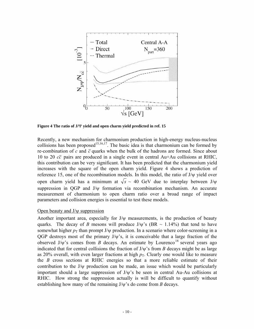
Figure 4 The ratio of J/Ψ yield and open charm yield predicted in ref. 15 Recently, a new mechanism for charmonium production in high-energy nucleus-nucleus collisions has been proposed15,16,17. The basic idea is that charmonium can be formed by re-combination of c and c quarks when the bulk of the hadrons are formed. Since about 10 to 20 cc pairs are produced in a single event in central Au+Au collisions at RHIC, this contribution can be very significant. It has been predicted that the charmonium yield increases with the square of the open charm yield. Figure 4 shows a prediction of reference 15, one of the recombination models. In this model, the ratio of J/ψ yield over open charm yield has a minimum at s ~ 40 GeV due to interplay between J/ψ suppression in QGP and J/ψ formation via recombination mechanism. An accurate measurement of charmonium to open charm ratio over a broad range of impact parameters and collision energies is essential to test these models.
Open beauty and J/ψ suppression Another important area, especially for J/ψ measurements, is the production of beauty quarks. The decay of B mesons will produce J/ψ’s (BR ~ 1.14%) that tend to have somewhat higher pT than prompt J/ψ production. In a scenario where color-screening in a QGP destroys most of the primary J/ψ’s, it is conceivable that a large fraction of the observed J/ψ’s comes from B decays. An estimate by Lourenco18 several years ago indicated that for central collisions the fraction of J/ψ’s from B decays might be as large as 20% overall, with even larger fractions at high pT. Clearly one would like to measure the B cross sections at RHIC energies so that a more reliable estimate of their contribution to the J/ψ production can be made, an issue which would be particularly important should a large suppression of J/ψ’s be seen in central Au-Au collisions at RHIC. How strong the suppression actually is will be difficult to quantify without establishing how many of the remaining J/ψ’s do come from B decays.

- 11 -
Thermal di-lepton and open charm The hot and dense system that is created in the heavy ion collision should emit electro-magnetic radiation during its time evolution, either in the form of real photons, or in the form of virtual photons, which materialize as lepton pairs. This thermal electro-magnetic radiation directly probes the dense system. The production rate of the thermal di-leptons is a steep function of temperature, and thus an accurate measurement may enable us to determine the initial temperature of the system.
Figure 5 The di-electron effective mass distribution in PHENIX central arm acceptance in central Au+Au collision at NNs = 200 GeV predicted by Rapp19. In the intermediate mass region (1 < Mee < 2.5 GeV), the dominant sources of electron pairs are open charm and thermal radiation from the QGP and hot hadronic gas. There are several processes that contribute to the di-lepton continuum. Qualitatively, the Drell-Yan process dominates the high-mass region, while thermal pairs from the hadron gas dominate the low-mass region. At RHIC energies, thermal radiation from the quark-gluon plasma is predicted to be the major source of di-leptons in the intermediate mass region of 1<Mee<3 GeV. In this mass range thermal radiation competes with a large background from semi-leptonic decays of correlated DD pairs. Figure 5 19 compares predictions for the thermal di-electron continuum above the φ resonance to di-leptons from open charm. The di-electron yield from open charm is comparable to the thermal di-lepton signal at Mee=1 GeV, and is two to three times as large in the mass range of 1.5 to 2.5 GeV. It is clear that one cannot extract the thermal dilepton yield without knowledge of open charm contribution. Knowledge of single electron production from open charm is insufficient to subtract this contributions, since the mass of the di-lepton also depends on the correlation between the D and D mesons. Thus it is imperative to directly measure the di-lepton spectrum from correlated charm pairs in order to observe and to accurately determine the thermal di-leptons from the quark-gluon plasma. This measurement will only be possible with the VTX upgrade.

- 12 -
High pT phenomena with light flavor in 10 – 15 GeV/c in pT The suppression of the high pT particle production is probably the most direct evidence of formation of very dense matter in high-energy nucleus-nucleus collisions at RHIC so far. The creation of dense matter is now firmly established from the high pT data in Au+Au collision and the comparison data in d+Au collisions. The natural next step is to extend the data, now in pT range of up to 10 GeV/c, to reach much higher pT to study the nature of the high pT suppression. In the present PHENIX detector, the pT range of the charged particle measurement is limited to 10 GeV/c in pT due to a large background from photon conversion and decay in flight of light mesons. The present central arm spectrometer suffers from these backgrounds since it measures particle tracks only outside of the magnetic field. Thus, it cannot distinguish a real high pT track that originates from the event vertex from a background track that is produced far from the vertex either by photon conversion or by decay-in-flight. The VTX detector will eliminate these backgrounds by providing additional tracking near the event vertex. In addition, the VTX measurement will improve the pT resolution by about a factor of three (see 3.4) by measuring the initial emission angle of the track in a slightly increased magnetic field. Combined, the pT range of the charged particle measurement in PHENIX will be extended to beyond 15 GeV/c or more, and will be limited only by the statistics.
Measurement of Upsilon states Given sufficient RHIC luminosity, we will be able to measure the ϒ-states ( bb bound states), and to compare closed and open-beauty production. It is particularly interesting to measure the relative yield of the three ϒ states, as we can study the suppression of heavy quarkonia as function of the binding energy in a region of large binding energy that is not accessible by charmonium production. In addition, unlike charmonium, the contribution to ϒ production due to quark recombination must be negligible since the number of bb pairs produced in an event is very small. Thus in the ϒ production we can directly access the de-confinement effect in dense matter. As mentioned previously with the VTX detector, the momentum resolution will be improved by about factor three, which reduces the mass resolution to ~ 60 MeV so that a clean separation of the 1S, 2S and 3S ϒ states becomes possible. However, this measurement will only be possible if luminosities significantly above the RHIC design value of 2×1026 cm-2 are reached.
2.2 Determination of spin structure of nucleon.
Exploring the spin structure of the nucleon: The past Most of what we know about the origin of the nucleon spin comes from Deep Inelastic Scattering (DIS) experiments performed over the last three and half decades. These experiments used polarized electron or muon beams in the momentum range 20-200

- 13 -
GeV/c to impinge on stationary polarized gaseous or solid-state targets. The partonic interaction that occurs in such experiments is between the virtual photons (coming from the polarized lepton beams) and the quarks inside the nucleons of the stationary targets. Naturally, DIS is an excellent probe of the quark polarization in the nucleons. In the late 1980s, measurements were made for the first time at higher energies and a significant deficit in the quark contribution to the nucleon spin was discovered. Often called in the literature “Spin Crisis”, the quest to understand this deficiency has driven the experimental and theoretical work in the field of nucleon spin since then. Where is the rest of the nucleon spin? The obvious place to look is the gluons and to measure their contribution. The virtual photons in the DIS only interact weakly with the gluons, as such, one can access the gluon spin dynamics in DIS only through scaling violations of spin structure functions which requires their measurement over a large range of x and Q2. As of today, such an experimental facility is unavailable and so one has to consider other techniques and tools to access the gluon spin.
Gluon polarization measurement at RHIC: The new tool that we have been waiting for is the Relativistic Heavy Ion Collider (RHIC). It enables collisions between polarized proton beams at high energy (up to 250 GeV/c). The expected luminosities at these top beam energies are 2x1032 cm-2 sec-1. As of now, 100 GeV/c polarized protons have been collided with a few x 1030 cm-2 sec-1 luminosity. Since protons are abundant sources of gluons, polarized proton-proton collisions allows a direct exploration of the gluon spin dynamics at the partonic level. The differences in the hadronic final states originating from gluon-gluon and quark-gluon interactions in the polarized proton collisions measured by the detectors when the proton spins in the two colliding beams are aligned vs. anti-aligned gives us access to the gluon spin contribution to the proton. For a partonic interaction of the kind (a+b c+d) occurring in polarized p+p collisions, assuming factorization one can write:
)( dcbaabb
aaA LLLL +→+
∆∆= (1)
Here ∆a/a and ∆b/b are the ratios of polarized to unpolarized distributions for parton distributions of a and b respectively, and aLL is partonic analyzing power calculable in pQCD. ALL is the double spin asymmetry measured in the experiment as a result of the polarized proton proton scattering for the final state in which c and d are created and measured in the detector. In this particular example, either a or b or both could be gluon distributions in the colliding protons. In the PHENIX experiment we will measure gluon spin polarization ∆G/G using many different processes. A partial list includes gg, gq in the partonic initial state resulting in different final states:
1) inclusive neutral and charged pions ),( ,0 XgqggaLL +→ ±π
2) inclusive photon production (direct or prompt photon production) ),( XgqggaLL +→ γ

- 14 -
3) charm & anti-charm and beauty-anti-beauty pair production ),,( XbbccgqggaLL +→
4) direct photon production along with jet ),( XjetgqggaLL ++→ γ
For different final states, experimentally we measure the following double spin asymmetry (a counting rate asymmetry):
−+++
−+++
+−
=NRNNRN
PPA
YBLL *
**1 (2)
Where PB/Y are the blue and yellow beam polarizations, N++/+- the counting rates measured with the ++(parallel) and +-(anti-parallel) orientations of the proton beam spin vectors and R is the ratio of luminosities for ++ and +- spin orientation collisions. (Ideally, R=1).
The role of VTX Detector: The different channels with which PHENIX can make measurements of the gluon polarization cover different kinematical regions in x and Q2. Figure 6 shows the x coverage possible with RHIC p+p running at 200 GeV center of mass, ~70% beam polarization and ~300 pb-1 luminosity (delivered) with the PHENIX detector for the above mentioned physical processes under two different scenarios. Here x is the gluon momentum fraction of the proton momentum, and “coverage” implies we measure the ratio ∆G/G with ~20% relative uncertainty of its expected value at that x. The baseline PHENIX detector is capable of covering a range: 0.02 < x < 0.3 (shown in blue). We note that although the coverage extends over one decade in x, between the different channels there is little overlap. The coverage extended by the VTX detector is shown in the same figure (in red). The proposed silicon vertex detector will be crucial in the determination of gluon distribution in two significant ways:
1) Different measurements will cover the same kinematic regions: this would enable the much-needed cross-checks within PHENIX for accessing the polarized gluon distribution. The vertex detector extends the reach in x for many of the measurements and hence adds a significant amount of overlap in x-range coverage.
2) By being able to observe displaced vertices at low-pt for semi-leptonic decays of charm and beauty, the VTX detector enables a larger x-range over which we will make gluon polarization measurements. It is estimated that the x reach of the silicon-vertex upgraded PHENIX will be 0.01 < x < 0.3.

- 15 -
Figure 6 Expected x-ranges for polarized and un-polarized gluon distribution measurements in PHENIX using different channels. The blue bars indicate the PHENIX detector’s existing capability while the red bars indicate the enhanced coverage provided by the proposed silicon vertex detector upgrade to PHENIX.
Since the two measurements of open charm and beauty and of γ+jet crucially depend on the silicon vertex detector more details are provided on these two channels below.
The heavy quark physics (open charm and beauty production) By requiring an additional cut on displaced vertex information coming from the vertex detector, we gain significantly in the robustness of the heavy-quark results by improving the purity of the event sample. We plan to observe charm production through its semi-leptonic decay to e±. We will need a good vertex resolution to identify the displaced vertices in such events. The main backgrounds expected for this physics include Dalitz decays and photon conversions. This has been studied (Section 3.2) using a GEANT detector simulation. We estimate that the SVTX could achieve ~50 µm DCA resoluiton. Using a DCA cut value ~200 µm for tracks with pT > 1 GeV/c, we should be able to achieve a significant background reduction. As a result of the DCA cut the purity of the event sample increases from ~50% to ~90% (see Figure 17 in section 3.2). Another possible channel to access gluon distributions is open beauty production. Beauty production measured at the Tevatron at 1.8 TeV, and the next-to-leading order pQCD calculation missed the data by factor of 2 or greater. The discrepancy between the

- 16 -
experimental data and the theory has sparked much debate and excitement recently. New data on beauty production would be crucial, especially at RHIC, since they would be obtained at different values of √ s (200 and 500 GeV). Measurements of beauty production can be performed in the present PHENIX detector using electron-muon coincidence using the central and forward muon arms. With the limited acceptance for the detector subsystems, this results in a narrow kinematics coverage and small detection cross section. With the VTX detector, we have two additional channels to measure beauty production at RHIC: the single electron in the central arm and B J/ψ+X. The single electron channel provides us much higher statistics compared with the µ-e channel. The main background in the b physics measurements is expected from the charm semi-leptonic decay, Dalitz decays, and photon conversions. Information provided by the VTX detector will enable a cut on the DCA to produce a highly pure sample of events involving beauty quarks with less than ~10% impurity from charm quark events in the low pT range (< 3 GeV) and even purer b-sample at higher pT. Without the VTX this impurity is expected to be more than 75% (see Figure 24, section 3.2). The VTX and the DCA analysis of data it will thus produce a reliable data set highly devoid of charm events and other impurities for the comparison with theory for beauty production cross section. The displaced vertex resolution possible with the VTX detector enables additionally one more measurement: B J/ψ+X. B mesons could be identified with J/ψ decays detected as displaced electron-pair vertices. This process identifies open beauty production with no charm contribution and will be a clean probe of the polarized and the un-polarized gluon distributions. Finally, a recent theoretical study (I. Bojak, Ph.D. Thesis, April 2000, Univ. Dartmund) of the expected values of the open charm and open beauty asymmetries at high energy concluded that they would be of the order of a few times 10-3 at RHIC energies. The open beauty asymmetries are expected to be slightly larger (private discussions with W. Vogelsang). False asymmetries related to bunch-to-bunch variation of luminosity in a collider are potentially a show-stopper for any spin measurement if they are comparable in magnitude to the asymmetry one is interested in. However, from the RUN 3 data analysis we already know at RHIC these false asymmetries can be controlled to be smaller than a few times 10-4. Although this situation could potentially get worse with the RHIC luminosity increase (due to difficulties associated with handling higher beam currents), additional tools are being discussed at RHIC that are expected to reduce uncertainties due to such effects by a factor of ~10 using techniques such as simultaneous spin flips in both RHIC beams using a spin flipper magnet and beam re-cogging. With such anticipated developments we will be able to pursue the open charm and open beauty spin physics measurements at PHENIX with the proposed Silicon Vertex detector.
Direct photon + Jet measurement:

- 17 -
One of the limitations of the direct photon measurement that is possible with existing PHENIX detector, is an imperfect determination of the partonic kinematics in the event. The uncertainty in the determination of the x of the gluon exists because we observe only a single photon in the final state. Event-by-event reconstruction of the event kinematics is impossible, and one has to rely on the Monte Carlo simulations to understand the event kinematics coupled to the detector acceptance. This has been studied (see section 3.3) using a PYTHIA simulation. The proposed VTX detector enables the tagging of the hadronic activity (originating from a single quark/jet), hence determination of the jet axis (Figure 26), and will significantly reduce the uncertainties stemming from the reconstruction of the parton kinematics (Figure 27). Our dependence on Monte Carlos is factored out. Additional uncertainties related to the determination the total jet energy, remain, however one does better by tagging the jet with the proposed VTX. PHENIX’s limited acceptance in rapidity as well as azimuth has been a significant hurdle in our measurement of any jet related physics. The VTX detector with its good hit resolution and large acceptance will serve as a high-resolution tracker and provide the much needed jet axis measurement in co-incidence with the direct photon measurement. Monte Carlo studies indicate a significantly improved determination of x-gluon (20% relative compared to ~40% without the VTX). The VTX detector can also be used to detect charged tracks around the direct photon candidate. This may allow an improved isolation selection for the direct photon in the event. The VTX detector is hence crucial in determining the polarized gluon distribution using the direct photon channel. For this particular measurement it converts the PHENIX detector in to a high resolution - large acceptance detector.
Other advantages of the VTX Detector: There are other advantages of the silicon vertex detector, which we mention briefly in this section.
Background suppression for W physics event sample W physics at PHENIX allows a unique possibility to distinguish the flavor (u and d) dependence of quark structure function and its polarization: W+ is produced by collision of du + , while W- is produced by ud + . However, if one wants to explore W physics with electron final states in the central arm, backgrounds from hadrons can be a significant problem. Improved momentum resolution and (hence) background suppression is the way to reduce the background. Using information from the silicon vertex detector in the momentum reconstruction, the moment resolution is improved by a factor 2 or 3. In addition, the large solid angle coverage of VTX will allow us to apply an isolation cuts for the single electron candidate and thereby to improve S/B ratio of the W decay electron. In general, an electron from W decay is isolated from a jet activity, while the backgrounds (very high pT charged particle decays and high pT electrons from heavy quark decay) have associated jet activity around it.
- 18 -
Improved correlation measurements between particles It is expected that the large acceptance of the silicon vertex detector in rapidity and azimuthal coverage, will enable us understand correlations between particles produced in the hadron-hadron collisions. One important measurement is related to the transversity distribution: transversity structure function is as fundamental as any other (un-polarized and polarized structure function of the nucleon), but it is yet to be measured. It is a helicity odd object, and it needs to be measured in experiments as a product of another helicity odd object so that the product is helicity even. Measurements of this kind involve measuring many particles and their angular correlations in the final state in addition to possible hadronic jet activity in the primary interaction. One example of this is the Collins fragmentation function, which refers to a correlation between hadron distributions around the jet axis. The orientation of π+ π - (hadron-) pair is also expected to show correlation with the transverse fragmentation function in single transverse spin p+p scattering at RHIC. The Silicon vertex detector is expected to improve determination of this orientation in spite of the fact that lack of particle-ID associated with such an event will dilute the correlation. Through these correlation functions we plan to measure the transversity distribution. Needless to say, enhanced acceptance, resolution provided by the silicon vertex detector would be crucial for such a measurement.
2.3 Exploration of the nucleon structure in nuclei Proton-nucleus collisions not only provide important baseline information for the study of QCD at high temperatures, they also address the fundamental issues of the parton structure of nuclei. Since the discovery of the EMC effect in the 1980's, it is clear that the parton-level processes and structure of a nucleon are modified when embedded in nuclear matter20. These modifications reflect fundamental issues in the QCD description of the parton distributions, their modifications by the crowded nuclear environment of nucleons, gluons and quarks, and the effect of these constituents of the nucleus on the propagation and reactions of energetic partons that pass through them. Of particular interest is the depletion of low momentum partons (gluons or quarks), called shadowing, which results from the large density of very low momentum partons. For gluons at very low momentum fraction, x < 10-2, one can associate with them, following the uncertainty principle, a large distance scale. These high-density gluons then will interact strongly with many of their neighbors and by gluon recombination or fusion are thought to promote themselves to larger momentum fraction, thus depleting small values of x. In most pictures the overall momentum is conserved in this process and so the small x region gluon density is depleted while the moderate x region above that is enhanced. In recent years a specific model for these processes, called gluon saturation, has been discussed extensively by McLerran and collaborators21. Gluon saturation affects both the asymptotic behavior of the nucleon gluon distributions as x approaches zero and the modification of this behavior in nuclei, i.e. shadowing. At RHIC energies many of the observables are affected by parton distributions at small x where nuclear shadowing is thought to be quite strong. However, theoretical predictions

- 19 -
of the amount of shadowing differ by factors as large as three. For example, in the production of J/ψ in the large rapidity region covered by the PHENIX muon arms, models from Eskola et al (Figure 7) predict only a 30% reduction due to gluon shadowing, while those of Frankfurt & Strikman22 (Figure 8) or Kopeliovich23 predict up to a factor of three reduction. Results from the measurements of the d+Au run should help to clarify how much shadowing we have, but increased statistics from higher luminosity runs and more definitive measurements via observables that are sensitive to gluon structure functions over several channels will be necessary to test the theory with sufficient power to constrain the underlying QCD processes.
Figure 7 - Gluon shadowing from Eskola24 as a function of x for different Q2 values: 2.25 GeV2 (solid), 5.39 GeV2 (dotted), 14.7 GeV2 (dashed), 39.9 GeV2 (dotted-dashed), 108 GeV2 (double-dashed) and 10000 GeV2 (dashed). The regions between the vertical dashed lines show the dominant values of x2 probed by muon pair production from DDbar at SPS, RHIC and LHC energies.
In particular, it is clear that a precise knowledge of the shadowed gluon structure functions in nuclei is essential towards understanding several of the important signatures for QGP in heavy-ion collisions at RHIC, including open and closed heavy-quark production. Recombination models for J/ψ production, which might cause an enhancement of that production in heavy-ion collisions due to the large density of charm quarks created in a collision, must be constrained by an accurate measurement of the amount of charm produced given the shadowing of the gluon densities in the colliding nuclei. A number of other physics issues besides shadowing also need to be understood. Energy loss of partons in the initial state is thought to have a small effect at RHIC since the energy loss per fm, in most models, is thought to be approximately constant and small compared to the initial-state parton energies at RHIC. On the other hand, partons in the final state could show some effects of energy loss since their momentum is lower, while heavy-quarks are expected to lose less energy than light partons due to the dead-cone effect25. These issues are very important in the high-density regions created in heavy-ion collisions, but need a baseline for normal nuclear densities from proton-nucleus collisions. Another general feature of most produced particles comes from the multiple scattering of
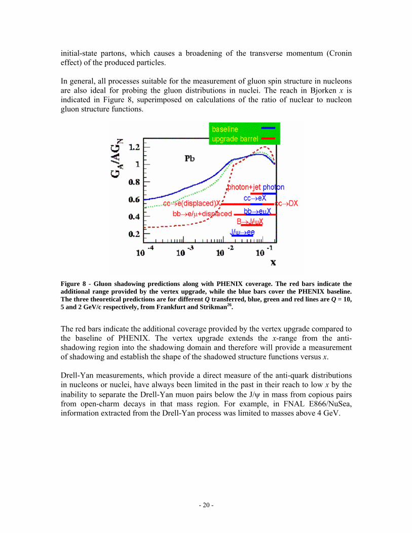
- 20 -
initial-state partons, which causes a broadening of the transverse momentum (Cronin effect) of the produced particles. In general, all processes suitable for the measurement of gluon spin structure in nucleons are also ideal for probing the gluon distributions in nuclei. The reach in Bjorken x is indicated in Figure 8, superimposed on calculations of the ratio of nuclear to nucleon gluon structure functions.
Figure 8 - Gluon shadowing predictions along with PHENIX coverage. The red bars indicate the additional range provided by the vertex upgrade, while the blue bars cover the PHENIX baseline. The three theoretical predictions are for different Q transferred, blue, green and red lines are Q = 10, 5 and 2 GeV/c respectively, from Frankfurt and Strikman26.
The red bars indicate the additional coverage provided by the vertex upgrade compared to the baseline of PHENIX. The vertex upgrade extends the x-range from the anti-shadowing region into the shadowing domain and therefore will provide a measurement of shadowing and establish the shape of the shadowed structure functions versus x. Drell-Yan measurements, which provide a direct measure of the anti-quark distributions in nucleons or nuclei, have always been limited in the past in their reach to low x by the inability to separate the Drell-Yan muon pairs below the J/ψ in mass from copious pairs from open-charm decays in that mass region. For example, in FNAL E866/NuSea, information extracted from the Drell-Yan process was limited to masses above 4 GeV.

- 21 -
Figure 9 - Dimuon mass spectrum from E866/NuSea27 showing the mass region used in their analysis which excludes masses below 4 GeV. Lower masses were excluded because of the large backgrounds from open charm in that region.
On the other hand, PHENIX, with the addition of a vertex detector, should be able to identify and quantify the portion of the lower mass dimuon continuum from charm decays and therefore isolate the Drell-Yan process at these lower mass and lower x values. In the central-rapidity barrel region values as low as x2 ~ 0.7×10⁻² could be accessed. This will still be a challenge because of the small cross sections and yields for Drell-Yan at RHIC, but has the potential of providing information on the anti-quark distributions at much smaller values of x. At the same time one would also learn more about charm production and the correlation of the charm pairs through the charm pairs found in the continuum. In summary, the silicon vertex barrel, which covers the PHENIX central arm mid-rapidity range ( |y| < 0.35 ), addresses the following physics in dA reactions :
• Charm and beauty at high pT and mid-rapidity via high-pT electrons and also exclusive decays such as πKD → and ππKD → .
• A gluon structure measurement in the anti-shadowing region as a baseline for shadowing measurements at small x.
• Charm measurements at mid-rapidity as a baseline for J/ψ production, i.e. for comparisons of open and closed charm which should share the same initial-state effects in nuclei.
• Accurate measurement of nuclear dependence of charm cross section • Beauty cross sections at mid-rapidity as a constraint on the contributions of
ψ/JB → to J/ψ production. • Comparison of light and heavy-quark pT distribution to determine differences in
energy loss and Cronin effects. • Better separation in high-luminosity measurements of ϒ measurements of the
three ϒ states. • Low-mass electron pairs and anti-quark shadowing at small x values.

- 22 -
For many of these topics the physics picture that can be obtained is significantly strengthened with the planned addition of an end-cap silicon vertex detector as described in Appendix A.

- 23 -
3. Physics measurements with the VTX detector The proposed VTX detector provides us the tool to measure new physics observables that are to date not accessible at RHIC or available only with very limited accuracy. These include a precise determination of the charm production cross section and transverse momentum spectra - particularly at high pT, a measurement of beauty, and the detection of recoil jets in direct photon production. In this section, we discuss how the proposed VTX detector makes these measurements possible, or significantly improves our capability to address these observables. Before discussing the simulation results and the expected performance of the VTX for each of the observables, we briefly explain the design of the proposed VTX detector and discuss the required performance. More technical details of the implementation of the VTX detector are presented in the section 4. In the last sub-section, we summarize the expected rate of physics signals and the physics reach that will become available with the VTX detector.
3.1 Design Considerations and the VTX detector geometry
Design Considerations The design considerations for the detector are
• ability to match tracks reconstructed in the central arms to hits or track segments from the silicon vertex detector.
• sufficient position accuracy so that the displacement resolution of the track with respect to the collision point is less than the cτ of charm and beauty decays, i.e. a resolution less than 100µm, preferably at the level of 30-50 µm.
• high resolution predominantly in rφ direction, i.e. the main bend plane of the magnetic field, matched to the central arm resolution.
A variety of simulations and first principle calculations have shown that the displacement resolution is dominated by the position accuracy of the two inner most detector layers and by the amount of multiple-scattering between the collision point and the two position measurements. Assuming that the multiple scattering occurs at the location of the first layer, the Distance to the Closest Approach (DCA) of a trajectory to the beam axis in the main bend plane can be measured with a resolution given approximated by:
( )θ
θσσ
σ 2
212
212
21
22
22
212
sin)(r
rrrr
msDCA +−+
≈
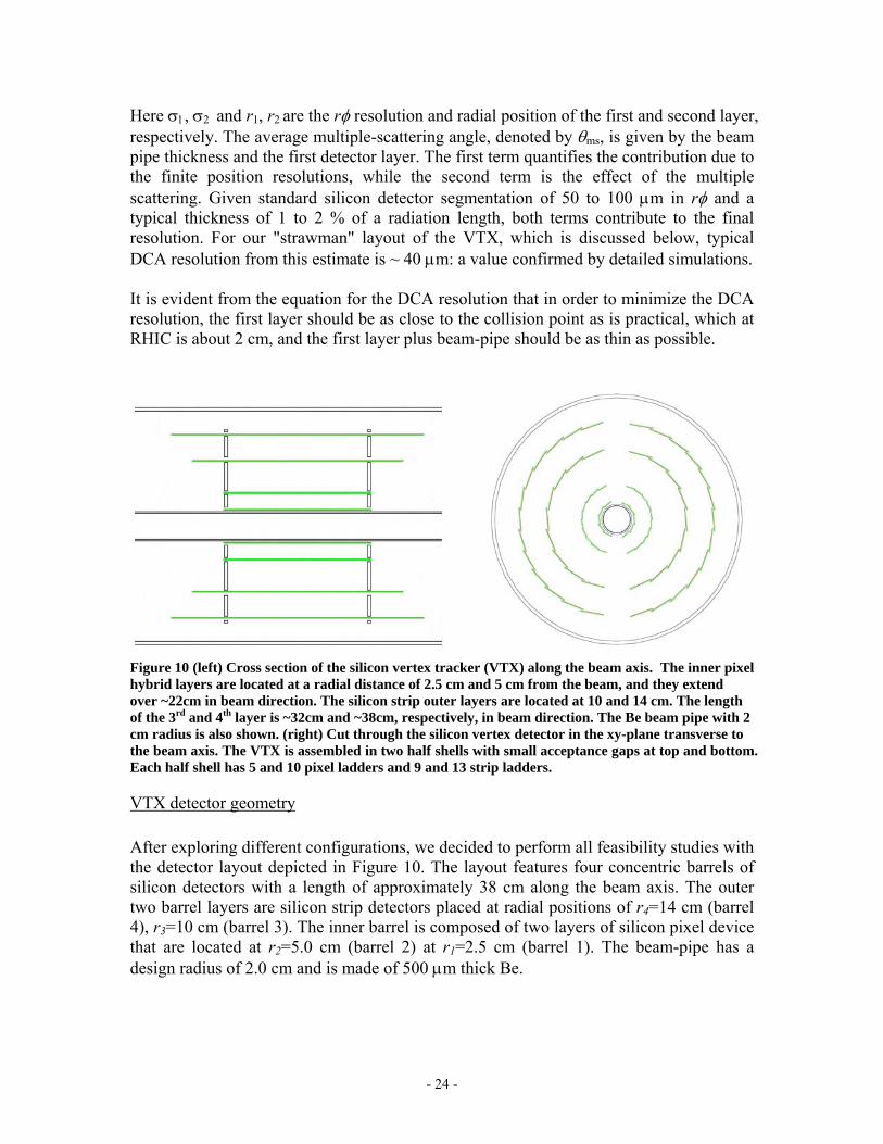
- 24 -
Here σ1, σ2 and r1, r2 are the rφ resolution and radial position of the first and second layer, respectively. The average multiple-scattering angle, denoted by θms, is given by the beam pipe thickness and the first detector layer. The first term quantifies the contribution due to the finite position resolutions, while the second term is the effect of the multiple scattering. Given standard silicon detector segmentation of 50 to 100 µm in rφ and a typical thickness of 1 to 2 % of a radiation length, both terms contribute to the final resolution. For our "strawman" layout of the VTX, which is discussed below, typical DCA resolution from this estimate is ~ 40 µm: a value confirmed by detailed simulations. It is evident from the equation for the DCA resolution that in order to minimize the DCA resolution, the first layer should be as close to the collision point as is practical, which at RHIC is about 2 cm, and the first layer plus beam-pipe should be as thin as possible.
Figure 10 (left) Cross section of the silicon vertex tracker (VTX) along the beam axis. The inner pixel hybrid layers are located at a radial distance of 2.5 cm and 5 cm from the beam, and they extend over ~22cm in beam direction. The silicon strip outer layers are located at 10 and 14 cm. The length of the 3rd and 4th layer is ~32cm and ~38cm, respectively, in beam direction. The Be beam pipe with 2 cm radius is also shown. (right) Cut through the silicon vertex detector in the xy-plane transverse to the beam axis. The VTX is assembled in two half shells with small acceptance gaps at top and bottom. Each half shell has 5 and 10 pixel ladders and 9 and 13 strip ladders.
VTX detector geometry After exploring different configurations, we decided to perform all feasibility studies with the detector layout depicted in Figure 10. The layout features four concentric barrels of silicon detectors with a length of approximately 38 cm along the beam axis. The outer two barrel layers are silicon strip detectors placed at radial positions of r4=14 cm (barrel 4), r3=10 cm (barrel 3). The inner barrel is composed of two layers of silicon pixel device that are located at r2=5.0 cm (barrel 2) at r1=2.5 cm (barrel 1). The beam-pipe has a design radius of 2.0 cm and is made of 500 µm thick Be.

- 25 -
The pixel detectors for the inner barrel layer have a segmentation of 50 µm by 425 µm. The outer layers are assumed to have 80 µm × 3 cm strips. This choice together with the radial location guarantees that the occupancy of the innermost strip layer (barrel 3) remains about 4.5% even in central Au-Au collisions. In the low occupancy environment of p+p collisions a stereoscopic readout of the strip layers reduces the effective channel size to 80µm × 1000µm. These detectors have been implemented as our "strawman design" into the GEANT simulation of the PHENIX detector. At this point no details of cooling, mechanical support, cables etc. are put into the simulation, however these materials are approximated by an effective thickness of the detector layers. From a survey of existing silicon detectors we conclude that a thickness of 2% of a radiation length per layer should be achievable while 1% of a radiation length will be challenging. We have chosen these two values for this effective thickness, 1% and 2% of a radiation length, to bracket the potential range of thickness and performed simulations with both values.
Detector Occupancy The occupancy of the each layer is calculated by using a GEANT model of the VTX detector integrated into the standard PHENIX simulation program, PISA. We use HIJING event generator to generate central Au+Au collision event, and feed the generated events into PISA with the VTX detector. In the simulation, we use a simplified model of the VTX signal generation. Charge sharing among the pixels and strips is accounted by the length of track segment projection onto the pixel or strip area. In this simplified simulation, no effect from charge diffusion in the sensor is taken into account. Since the size of charge diffusion (~ 10 µm) is much smaller than the strip width (80 µm), the dominant part of charge sharing effect is included in the simulation. Table 1 Occupancy of the VTX layers for central Au+Au collisions at 200 GeV. HIJING event generator and a GEANT model of the VTX detector is used to calculate the occupancy.
Layer radius Detector Occupancy Layer 1 2.5 cm Pixel 0.53 % Layer 2 5.0 cm Pixel 0.16% Layer 3 10.0 cm Strip 4.5 % (x-strip) 4.7 % (u-strip)Layer 4 14.0 cm Strip 2.5 % (x-strip) 2.7 % (u-strip) The result of the simulation is summarized in Table 1. The occupancy is lowest at about 0.16 % for the second pixel layers. The third layer, or the first strip layer, has the highest occupancy of about 4.5%. The calculated occupancy is about twice the value if there were no charge sharing effect. The physics observables discussed in this proposal use hits from the VTX in two ways.

- 26 -
1. Tracks from the central-arm are projected to the VTX layers, and the hits in the VTX are associated with the track. The accurate VTX hit information is then used to refit the track and a DCA is calculated to the collision vertex.
2. In standalone tracking, hits from the four VTX layers are collected and used to form track segments.
The tools to associate hits with tracks and refit are reasonably well-developed and they are described below, while the stand-alone tracking is in early stages of development.
Central Track – VTX matching In order to make full use of the VTX capabilities, tracks reconstructed in the central arms have to be matched to hits or track segments in the VTX. We use the known magnetic field to project central arm tracks to each of the layers in the VTX. Figure 11 shows the residual between the track projection of 2 GeV/c pions and the hit location in φ and z for the inner-most pixel layer. The hit positions in the VTX detector have not been used at this stage of the track and hit matching. The distributions are centered at zero and have a width of 5 mrad and 0.05 cm. Similar residual distributions are found for each of the four VTX layers.
Figure 11 The residual between track projection and hit location in φ and z for the inner-most pixel layer. This simulation is for 2 GeV/c pions.
For tracks from D Kπ decays the residual distribution is expected to be broader, since the central arm tracking assumes the track originated at the collision vertex. This is verified in Figure 12, which shows the residuals for tracks from D Kπ decays, again the inner-most layer of the VTX. The residuals are significantly larger than for primary tracks. It is important to choose the matching criteria for hits to central arm tracks to be broad enough to include also the tracks from open charm and beauty decays. For each VTX layer the hit-association assigns to each central arm track the hit closest to the track projection within a certain window. Currently the size of the window is taken to be 30 mrad in φ and 0.15 cm in z for the pixel layers, i.e. several times the widths of the residuals found in the D Kπ decay shown in Figure 12. The window size is changed to

- 27 -
30 mrad in φ and 0.45 cm in z for the strip layers. A future improvement of the algorithm will be based on momentum dependent matching window.
Figure 12 The residual between track projection and hit location in φ and z for the inner-most pixel layer. The VTX hits are not included in the fit. This simulation is for D Kπ at pT = 2 GeV/c.
The number of random charged particles inside of the initial matching window is about 0.1 for the most central Au+Au collisions. The matching window size can be further reduced after the track fitting using the hits in the VTX, eliminating most accidental matches. The residual distribution between the track fit and the VTX hit position in the inner-most pixel layer is shown in Figure 13 for prompt pion and in Figure 14 for particle from D Kπ decay. The RMS width in φ and z are reduced to 1.6 mrad and 126 µm for prompt pion at 2 GeV/c. For tracks from D Kπ decays, which have lower momentum in average, the RMS width of the residual is 2.2 mrad and 150 µm. The solid angle of the 3 σ matching window is then reduced to about 0.1 mstr and the occupancy in the window is about 1% for the most central collision.
Figure 13 The residual between the track and the hit location in φ and z for the inner-most pixel layer after the hits in the VTX are included. This simulation is for 2 GeV/c pion.

- 28 -
Figure 14 The residual between the track and the hit location in φ and z for the inner-most pixel layer after the hits in the VTX are included. This simulation is for D Kπ at pT = 2 GeV/c.
After the hits in the VTX detector are associated with the track, the distance of closest approach of the track to the primary event vertex (DCA) is calculated in the plane transverse to the beam. We base this calculation on the inner-most two pixel layers. Figure 15 shows the DCA distribution for pions at pT = 2 GeV/c. A DCA resolution of 36 µm is achieved, which is consistent with the 50 µm pixel width of the detector.
Figure 15 The DCA distribution for 2 GeV/c pions in the PISA simulation of the VTX detector. The DCA resolution of σ=36 µm was achieved using the two inner-most two pixel layers.
We have also evaluated the effect of the hit occupancy expected in central Au+Au collisions on the matching resolution. The statistics of this simulation is limited, but the result shows that the resolution only slightly deteriorates. For example, for the inner most pixel layer, the RMS of the residual in φ increases from 2.2 mrad to 2.5 mrad, and the RMS of the residual in z increase from 150 µm to 230 µm. The study of the high multiplicity on the DCA resolution is underway.

- 29 -
3.2 Open Charm and Beauty Measurement
Open Charm measurement from semi-leptonic decay Open charm and beauty spectra and yields are a sensitive probe of the early stages of heavy-ion collisions, and are keys for the physics goals of gluon spin structure and for structure function studies in pA reactions. For heavy-ion collisions, the goal is to improve the accuracy and precision of the charm measurement, and to extend the reach to higher pT to measure the energy-loss of open charm. The yield of beauty in heavy-ion collisions should be dominated by the initial hard collisions and hence will serve as a critical benchmark for the first stage of reaction. For open charm our strategy is to use semi-leptonic decays to electrons in a wide pT range and to complement this at high pT with hadronic decay channels. The four layers of the central silicon barrel provide an accurate measurement of the trajectory and impact parameter of tracks near mid-rapidity. Single electrons at different momenta were simulated and tracked through the GEANT implementation of PHENIX including the straw-man vertex detector. The simulation was run with 9kG magnetic field. The hits from the electrons were tracked back to calculate the transverse distance-of-closest approach (DCA) to the known point-of-origin. For all cases the DCA resolution is better than or comparable to the cτ of charm and beauty decays.
Figure 16 DCA distribution for electrons from Dalitz, charm and beauty decays simulated through four 1% Si layers on the left and four 2% layers on the right.

- 30 -
The power of this resolution is seen by comparing the distribution of DCA from charm, beauty and Dalitz decays of π0 in Figure 16. The spectra were generated from p+p events (PYTHIA) passed through GEANT. The design thickness for the inner pixel layer is 1.2% of radiation length (X0) and for the outer barrel layers is 2.0 % X0. For these simulations we bracket the range of possibilities by running simulations with either 1% or 2% X0 per layer. In the bottom panels of Figure 16 are the DCA distributions for electrons above 1 GeV/c. A DCA cut of 200 µm removes the majority of Dalitz contribution from the electron yield. Note that this is the momentum of the electron and given the large Q-value of the D decay, these electrons predominantly come from low-momentum D’s. Since beauty decays have longer lifetimes, the electrons from B decays dominate at large DCA values. By fitting the full DCA distribution with the expected shapes from the different cτ we should be able to simultaneously extract integrated charm and beauty yields for electron momenta above 1 GeV/c. Below 1 GeV/c the extraction is more difficult, but even down to 500 MeV/c charm dominates the DCA distribution above 200 µm for a thickness between 1 and 1.5 % of a radiation length. In particular, the vertex detector will provide a dramatic improvement over the previous measurement, which was limited to ~25 % systematic error resulting from the uncertainties in the background subtraction. Figure 17 shows the “signal to noise” for the optimistic (1 % X0) and pessimistic (2 % X0) cases compared to the measurement without the vertex detector available. This should allow a much cleaner extraction of the background-subtracted electron spectra for pT>0.4 GeV/c than was previously available, including the charm-specific d2Ne/dydpT for electrons up to about 2.5 GeV/c.
Tcutp0 1 2 3
char
m e
lect
ron
s S
ign
al/B
kgd
.
10-1
1
10
102 /Layer00.01 X
/Layer00.02 X
No DCA cut
Figure 17 Signal to Background ratios as a function of minimum electron pT cut. The signal corresponds to detached electrons from charm decays using a DCA cut of 200µm (circles) or no DCA cut (diamonds). The background corresponds to electrons from Dalitz decays and photon conversions which pass the corresponding DCA cuts, assuming four layers of Silicon with 1 or 2% of a radiation length per layer.
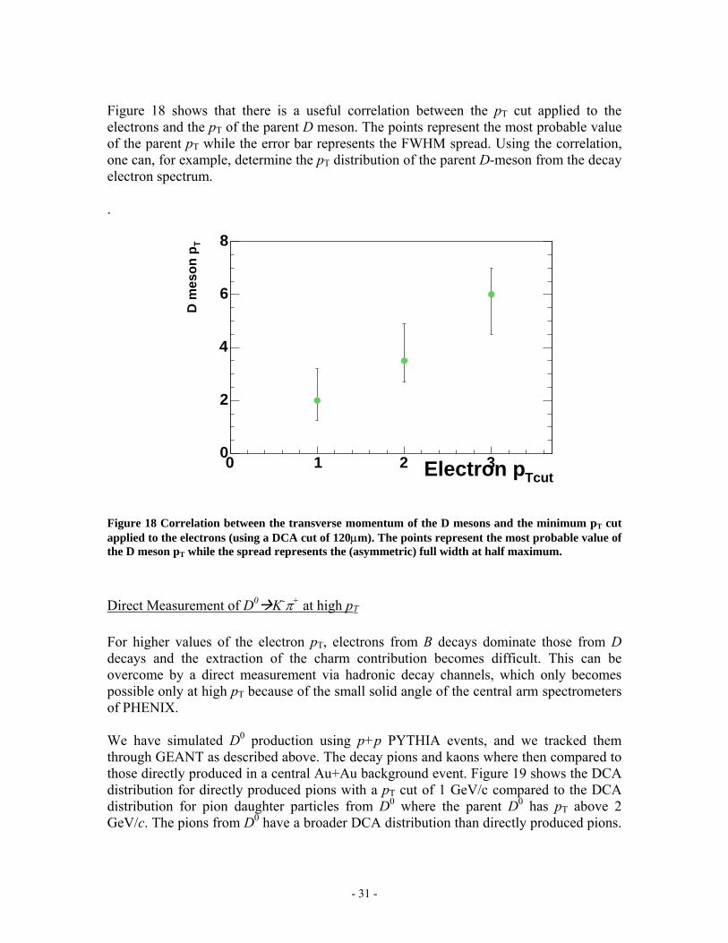
- 31 -
Figure 18 shows that there is a useful correlation between the pT cut applied to the electrons and the pT of the parent D meson. The points represent the most probable value of the parent pT while the error bar represents the FWHM spread. Using the correlation, one can, for example, determine the pT distribution of the parent D-meson from the decay electron spectrum. .
TcutElectron p0 1 2 3
TD
mes
on
p
0
2
4
6
8
Figure 18 Correlation between the transverse momentum of the D mesons and the minimum pT cut applied to the electrons (using a DCA cut of 120µm). The points represent the most probable value of the D meson pT while the spread represents the (asymmetric) full width at half maximum.
Direct Measurement of D0 K-π+ at high pT
For higher values of the electron pT, electrons from B decays dominate those from D decays and the extraction of the charm contribution becomes difficult. This can be overcome by a direct measurement via hadronic decay channels, which only becomes possible only at high pT because of the small solid angle of the central arm spectrometers of PHENIX. We have simulated D0 production using p+p PYTHIA events, and we tracked them through GEANT as described above. The decay pions and kaons where then compared to those directly produced in a central Au+Au background event. Figure 19 shows the DCA distribution for directly produced pions with a pT cut of 1 GeV/c compared to the DCA distribution for pion daughter particles from D0 where the parent D0 has pT above 2 GeV/c. The pions from D0 have a broader DCA distribution than directly produced pions.
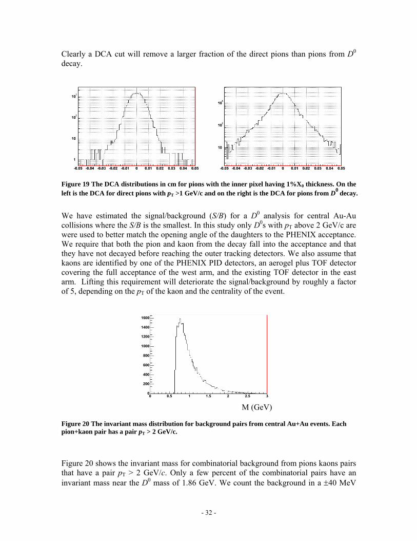
- 32 -
Clearly a DCA cut will remove a larger fraction of the direct pions than pions from D0 decay.
Figure 19 The DCA distributions in cm for pions with the inner pixel having 1%X0 thickness. On the left is the DCA for direct pions with pT >1 GeV/c and on the right is the DCA for pions from D0 decay.
We have estimated the signal/background (S/B) for a D0 analysis for central Au-Au collisions where the S/B is the smallest. In this study only D0s with pT above 2 GeV/c are were used to better match the opening angle of the daughters to the PHENIX acceptance. We require that both the pion and kaon from the decay fall into the acceptance and that they have not decayed before reaching the outer tracking detectors. We also assume that kaons are identified by one of the PHENIX PID detectors, an aerogel plus TOF detector covering the full acceptance of the west arm, and the existing TOF detector in the east arm. Lifting this requirement will deteriorate the signal/background by roughly a factor of 5, depending on the pT of the kaon and the centrality of the event.
Figure 20 The invariant mass distribution for background pairs from central Au+Au events. Each pion+kaon pair has a pair pT > 2 GeV/c.
Figure 20 shows the invariant mass for combinatorial background from pions kaons pairs that have a pair pT > 2 GeV/c. Only a few percent of the combinatorial pairs have an invariant mass near the D0 mass of 1.86 GeV. We count the background in a ±40 MeV
M (GeV)

- 33 -
window around 1.86 GeV. The window corresponds to ±2 times the rms mass resolution, which is 1% calculated from the known momentum resolution of the PHENIX tracking. To count the signal we scale the number of reconstructed D0's in the PYTHIA events by the number of binary collisions for a central Au+Au events. The signal/background (S/B) is then studied as a function of a simultaneous DCA cut on the pions and kaons. Figure 21 shows the S/B for different DCA cuts on pairs detected in the west-arm. The left- and right-hand panels are for simulations with 1% X0 and 2% X0 per layer. With no DCA cut the S/B is less than 0.1%, placing a DCA cut of 100 µm increases the S/B to a level of 2-3%. This S/B should be further improved by requiring that the parent particle point back to the collision vertex.
Figure 21 The S/B for D0 Kπ with a pt >2 GeV/c for central Au+Au events into the west-arm of PHENIX. On the left is the simulation for 1%X0 thickness per layer. On the right is simulation for 2%X0 thickness per layer.
Figure 22 The S/√B for D0+⎯D0->Kπ with a pt >2 GeV/c for central Au+Au events into the west-arm of PHENIX. On the left is the simulation for 1%X0 thickness per layer. On the right is simulation for 2%X0 thickness per layer.
The statistical significance of the signal can be estimated by BS / . This ratio can be interpreted as the number of sigma of the extracted counts in the signal over the fluctuating background. It increases with the square root of the number of events. Using the run assumptions described in section 3.5, we will approximately collect 200M central

- 34 -
Au+Au events within a ±10 cm collision window in a running period. Under these assumptions the combined (D0+⎯D0) S/√B for different DCA cut strategies for pairs detected in the west-arm of PHENIX is shown in Figure 22. From Figure 22, we can conclude that the D0 peak for particles above pT > 2 GeV/c can be extracted robustly. This is the worst case for the most central collisions where the combinatorial background is largest. Requiring the parent to point to the collision vertex can further reduce the background. Simulations indicate that at higher-pT the acceptance for D0 increases since the opening angle between the daughters is smaller while the combinatorial background due to decreases. For D0s above pT > 3 GeV/c, even though the open charm yield is lower, the significance of the (D0+⎯D0) peak maintains a level of 7 σ in central Au+Au collisions. In the simulation in this section, we use PYTHIA to generate D mesons. Recent results in p+p and d+Au at RHIC indicate that PYTHIA underestimate the yield of high pT D mesons more than a factor of 2. Therefore, the rate and the S/B estimate given this section should be considered as a lower limit.
Open Beauty Measurement B meson production, while rarer than D production, is somewhat simpler to measure with the VTX detector because of the larger cτ. The main challenge is the relatively low rate. We have at least two methods to measure B with the VTX detector:
• Semi-leptonic decays: Since beauty mesons have a larger lifetime than charm mesons, it is possible to extract the beauty yield at low transverse momentum from the distribution of decay distances. At large transverse momentum beauty decays dominate the DCA distribution.
• The decay channel B J/ψ produces J/ψ that are displaced from the collision. For momenta greater than 3 to 4 GeV/c electrons with displaced vertexes are dominated by beauty decays. This is clearly seen in Figure 23. By placing a DCA cut on the order of 150 µm we should be able to cleanly separate electrons from beauty from all other sources. Note however that this clean separation is only possible with the VTX detector even in this high pT region. Although the high pT region is dominated by beauty, there is a significant contribution from charm component, and the separation of these two components is possible only with the DCA measurement. With an accurate determination of the b component, the charm component will also accessible up to 6 GeV/c using a simultaneous fit of the DCA distribution. As discussed in the previous section, the high pT charm component will also be measured directly in D Kπ decay. The signal to background ratio for beauty decays at high momentum is shown in Figure 24. The effect of the DCA cut is even more favorable than for charm.

- 35 -
Figure 23 DCA distribution for electrons from Dalitz, charm and beauty decays simulated through four 1% or 2% Si layers
Tcutp0 1 2 3
bea
uty
ele
ctro
ns
Sig
nal
/Bkg
d.
10-2
10-1
1
10
102
103
/Layer00.01 X
/Layer00.02 X
No DCA cut
Figure 24 Signal to Background ratios as a function of the minimum electron pT cut. The signal corresponds to detached electrons from beauty decays using a DCA cut of 200µm (circles) or no DCA cut (diamonds). The background corresponds to electrons from Dalitz decays and photon conversions which pass the corresponding DCA cuts, assuming four layers of Silicon with 1 or 2% of a radiation length per layer

- 36 -
3.3 Photon and jets measurement in polarized p+p Direct photon emission is a key process to measure the gluon distribution in the nucleon and the polarization of the gluons. Because quark-gluon Compton scattering, q+g q+γ is the dominant parton-level process of the production of high pT direct photons in p+p collisions at RHIC energies, the cross section of this process is directly proportional to the quark and gluon densities multiplied by the pQCD cross section. Thus measuring the direct photon together with the recoil jet is a direct and a clean way to measure the gluon density and polarization as a function of the momentum fraction x. With the present PHENIX setup, direct photons are measured with the finely segmented electromagnetic calorimeters (EMCal) in the central arms. However, due to the limited coverage of the central arm tracker, most of the recoil jet cannot be detected or identified. Therefore we can only measure the inclusive direct photon averaged over the recoil jet kinematics. From data of other experiments, it has been found that there is discrepancy between experimental data of the inclusive direct photon spectra and pQCD calculations. Although the discrepancy can be explained by e.g. intrinsic kT phenomenology, it is important to investigate the photon-jet correlation experimentally to understand it. In p+p, p+A, and light ion collisions, the VTX detector works as a stand-alone, large solid angle charged particle tracker. The expected momentum resolution for tracks reconstructed solely by the VTX detector is about 10% for a 1 GeV/c track. This resolution is sufficient to reconstruct recoil jets in wide rapidity range (|η|<1). With the knowledge of the recoil jet we can constrain the initial kinematics (x1 and x2) of incoming partons and thus determine the gluon density and polarization as function of x. We have studied the potential improvements due to the VTX detector in a Monte Carlo simulation. In the simulation, the direct photon events have been generated using the PYTHIA event generator at a fixed interaction point. The recoil jet is then reconstructed from the charged tracks within the VTX detector acceptance (|η|<1.2) but in the opposite azimuthal direction of the direct photon. In the first step of the algorithm, tracks with momentum greater than 1 GeV/c at an azimuth angle opposite to the direct photon (|φ – φγ| > π/2) are selected. Then, the direction of the jet is estimated as the momentum weighted average of the selected tracks, as:
∑∑
∑∑ == i
T
iT
ijet
iT
iT
ijet
pp
pp φ
φη
η ,
Next, the tracks with momenta above 1.0 GeV/c and within the cone of radius 5.0)()( 22 <−+−= ijetijetR φφηη are selected. In a second iteration the recoil jet axis
is corrected with the same algorithm, using the tracks within the cone. This procedure is iterated until the direction of the axis no longer changes.

- 37 -
Figure 25 In each panel, the green histogram shows the pseudo-rapidity, ηq-distribution of the final hard scattered partons, which initiated the recoil jet; the blue histogram shows the ηq-distribution of recoil jets within the barrel VTX acceptance; and the red histogram show the (ηjet -ηq)-distribution, where ηjet is for the pseudo-rapidity reconstructed for the recoil jets. Different panels are for the event samples with direct photon of different transverse momenta, starting from 4-5 GeV/c in the upper left to 9-10 GeV/c in the lower right panel.
Figure 25 illustrates how well the direction of the recoil jet is determined by this simple algorithm. In the figure, the pseudo-rapidity ηq of the scattered quark (obtained from the event generator) are plotted as green histograms. The blue histograms in the figure show the distributions of ηq for events in which the recoil jet is reconstructed within the VTX acceptance. The red histograms show the difference ηq - ηjet between the true pseudo-rapidity of the recoil quark and that of the reconstructed jet. The large uncertainty of the recoil jet kinematics, as seen from the wide distribution of ηq, is much reduced by the reconstruction of the recoil jet direction.
From the measurement of ηjet and the transverse momentum pT of the direct photon, the kinematics of the initial partons can be determined. Under the assumption that the pT of the direct photon and the recoil jet is the same, the fractional momentum of initial partons x1 and x2 are determined from the following relations:

- 38 -
))sinh()(sinh(2
)(2
)),cosh()(cosh(2
)(2
21
21
γγ
γγ
ηη
ηη
+=+=−
+=+=+
jetTZ
jetZ
jetTjet
sppp
sxx
spEE
sxx
Thus x1 and x2 are calculated as:
))exp()(exp(
)),exp()(exp(
2
1
γ
γ
ηη
ηη
−+−=
+=
jetT
jetT
spx
spx
Because we cannot distinguish which of x1 or x2 corresponds to the gluon’s x, we assume:
],max[
],min[
21
21
xxx
xxx
quark
gluon
=
=
This is because the gluon distributes in the lower x region than the quark.
Figure 26 Top panels: correlation between x reconstructed and true x-value from PYTHIA. Bottom panels: (reconstructed-x – true-x) / true-x. In the plots on the left, ( ) 2
Tx P Sγγ = and no jet
information has been used. The plots in the right panel are obtained, using the reconstructed jet axes in the barrel VTX.

- 39 -
Figure 26 shows the correlation between the reconstructed x and its true value known from the event generator. If the recoil jet direction is unknown (left panels), the best estimate for x based on the photon pT is only loosely correlated to the true x. On the other hand, with the recoil jet reconstruction (right panels), there is a narrow correlation between the reconstructed x and its true value. How well initial gluon’s x can be extracted is summarized by Figure 27. Here, the mean values and widths (RMS) of (x(reconstructed) – x(true)) / x(true) are shown as a function of xgluon. The x-values are determined with an accuracy of ~20%.
Figure 27 The relative widths (RMS) of the (x(true) – x(reconstruct))/x(true) distributions, using the reconstructed jet axes in the barrel
3.4 Improved momentum resolution and pt resolution In the present PHENIX detector, drift chambers that are located outside of the central magnet measure the momentum of the charged particles. Since there is little magnetic field at the location of the drift chambers, charged particles traverse them on almost straight trajectories. The momentum p of a particle is related to the bending angle α measured at the drift chamber approximately as δp/p ~ 87 mrad/p (p in GeV/c). The momentum resolution of the central detector will be much improved with the VTX detector. This is because in the present PHENIX central arm spectrometers the effective field kick of 87 mrad GeV/c is only about 40% of the total angular deflection ∆φ in the magnetic field. The field integral at the location of the drift chamber is about 0.7 Tm,

- 40 -
which gives ∆φ = 210 mrad /p. Since the VTX measures the initial direction of the particles the full value of ∆φ is measured rather than the angle α at the edge of the magnetic field. In addition, a second field coil, which has been installed in 2003, allows increasing the field integral to roughly 1 Tm. With this field integral the total field-kick increases to 300 mrad GeV/c. The improvement in momentum resolution is directly given by the ratio of the field kicks ∆φ/ α ∼ 300 mrad / 87 mrad ~ 3. The higher momentum resolution with the VTX detector will improve the high pT measurements. At present, a momentum resolution of about 1%/p has been achieved. With the VTX detector, the resolution of a 30 GeV/c track can be reduced from 30% to about 10%. In addition, the track confirmation close to the vertex provided by the VTX will eliminate the decay and conversion background, which currently limits the pT reach of the PHENIX charged particle tracking to pT < 10 GeV/c. The improvement of the momentum resolution may have a significant impact on the data quality in the higher e+e- mass region around the ϒ states. With the better momentum resolution also the mass resolution decreases to a level that the members of the ϒ family, the resonances ϒ1S (9.46 GeV), ϒ2S (10.02 GeV) and ϒ3S (10.36 GeV) can be clearly separated. This is shown schematically in Figure 28. The VTX together with the increased magnetic field reduces the resolution at the ϒ states from ~170 MeV to ~60 MeV for the e+e- decay channel. Thus it allows separating the individual states. We note that this measurement will be a significant challenge and only possible if sufficiently high luminosities expected for RHIC II are available for extended running periods.
Figure 28 - Separation of Upsilon states in the di-electron spectrum with a vertex detector (yellow) and without (black). The number of ϒs in this plot represents our expectation for a Au-Au run with a recorded effective luminosity of ~1 nb-1 (see chapter 3.5).

- 41 -
3.5 First level trigger capabilities In central and mid-central Au+Au collisions the present PHENIX minimum bias trigger is sufficient to trigger and select events within the VTX acceptance with high efficiency. However, in p+p, p+A, light ion, and peripheral Au+Au collisions the min. bias trigger based on the PHENIX beam-beam counters has insufficient efficiency and vertex reconstruction accuracy. The VTX detector will allow overcoming the shortcomings of the present system. The inner most two layers of the VTX detector are made of Si pixel detector read-out by ALICE pixel chip (see section 4.2 for details). Each ALICE pixel chip provides a general OR of the 32×256 pixels every beam crossing. Thus 106 ns after the beam crossing tracking information about the event is available with a granularity of 160 channels, 10 slices in azimuthal angle φ and 16 slices in beam direction z, and 320 channel, 20 slices in φ and 16 in z, from the 1st and 2nd layer, respectively. The length of a chip along the beams axis is 1.36 cm. We have developed a trigger algorithm which analyzes this information in three steps:
1. Track segments in φ are generated by matching slices at the same φ location in the 1st and 2nd layer. Only events with 2 or more reconstructed φ track segments are processed further.
2. For each φ slice all hits in the 1st layer are combined with all hits in the 2nd layer. The z positions are extrapolated back to the beam axis to identify the possible vertex position. The result of the extrapolation (Figure 29) is histogramed with the same granularity as the z slices.
3. In the final step the maximum in the z histogram is found and required to be within 2 readout chip lengths of the VTX acceptance. Also, the size of the maximum is required to be greater than twice the number of possible tracks in the detector. This last requirement increases the rejection of events which would otherwise trigger due to noise and various physics processes.
Figure 29 Schematic of step 2 of the algorithm. The upper line corresponds to the outer layer, the middle line to the inner layer, and the lower line to the histogramed beam axis.
The algorithm was tested with 10000 min. bias p+p events generated by PYTHIA, which were tracked through the PHENIX GEANT simulation including the VTX. Figure 30

- 42 -
compares the generated event vertex distribution, which has a width of σ = 20 cm, to the distribution of the accepted events. Within the VTX acceptance 90±1% of all events are triggered. This is a substantial improvement over the 50% trigger efficiency of the system currently used in PHENIX. At the same time 95 out of 100 events outside of the VTX acceptance are rejected. As shown in Figure 31the trigger algorithm reconstructs the vertex with an accuracy of σ ~ 1 cm.
Figure 30 The red curve is shows the event vertex distribution, while the blue curve shows the accepted events. The vertical axis is plotted on a logarithmic scale.
Figure 31 Reconstruction of the vertex. The horizontal axis is the difference between the actual vertex and the position guessed by the algorithm.

- 43 -
The algorithm has also proved to be robust against lateral beam position variations within ±5 mm and against noise at a level of a few %, a level a factor of >10 larger than the performance of these chips observed in the NA60 experiment and in ALICE test beams. In the worst case scenario the efficiency and the rejection both deteriorated by about 6%. It is worth noting that for p+p collisions, the trigger efficiency improves with the multiplicity of the event. For hard processes, this algorithm is expected to have ~100% efficiency.
3.6 Event rate estimates In this section we estimate the event rates of selected physics processes corresponding to the major goals of the VTX detector. First, we summarize the common assumptions that go into estimating yields for the physics signals that the VTX detector will make available. We start with integrated luminosity estimates, based on the luminosity evolution at RHIC expected by the BNL Collider Accelerator Division. Then we fold in estimates of all of the practical efficiency factors that reduce the yields measured by PHENIX. The obtained “effective luminosity” is then used to estimate the signal yields. The efficiency factors are summarized in Table 2 for the p+p, d+Au and AuAu cases. The first three factors, (1) to (3), are the factors that reduce the CA-D delivered luminosity to the recorded luminosity that is written on data tape by PHENIX, and therefore they are common for all three beam species. These factors are based on the actual performance of RHIC and PHENIX during RUN2 and RUN3, and to be conservative we assume no improvements of these factors in the future. The largest loss of the recorded luminosity comes from the vertex cuts, factors (1) and (2) in the table. Here we used longitudinal length of the collision diamond of σ=20 cm and a vertex cut of |z|<10 cm since the inner-most layer of the VTX detector covers |z|< 11 cm. The combined reduction of these two factors is gives about 28%. With 60% PHENIX uptime, which was achieved in RUN3, the recorded luminosity is 17% of CA-D delivered luminosity. The effective luminosity is further reduced by the fraction of “good data” that can be used for offline analysis (the factor (a) ) and the offline reconstruction efficiency (the factors (b) and (c)). Again, these numbers are based on actual PHENIX performance and reconstruction efficiency (tracking plus electron identification) for single electrons in central arms in the RUN2 Au+Au data analysis. The reconstruction efficiency includes the loss due to the dead channels in the central arm detectors. The efficiency depends on the beam species, and it decreases from p+p to d+Au to Au+Au. This reduction is caused by occupancy dependent efficiency losses, which are also based on the actual performance in RUN2 data analysis. The reconstruction efficiency factors are shown for both single electron (factor (b)) and electron pairs (factor (c)). We should emphasize that the reality factors given in Table 1 are all based on achieved performance of RHIC and PHENIX and we assume no improvement in the future. Therefore the effective luminosity presented here is a very conservative estimate and

- 44 -
potential improvements will increase the effective luminosity usable by the VTX detector. In particular, improvement in diamond size of the beam and the efficiency of the storage RF would greatly increase the effective luminosity. In Table 3 we list the delivered integrated luminosity, the recorded integrated luminosity with the VTX (delivered integrated luminosity times factor (4) in Table 2), and the effective integrated luminosity. For the delivered integrated luminosity, we used the CA-D projection of the RHIC luminosity in year 2008 RUN and assume constant effort, which means 19 weeks of physics data taking per year. Since there is a very large variation of the CA-D luminosity projection, we use the average of the most pessimistic estimate and the most optimistic estimate. This luminosity estimate is consistent with the five year extended beam use proposal presented by PHENIX to the Physics Advisory Committee (PAC) in the fall 2003. The most optimistic luminosity figure is about a factor of 2 larger than shown in the table.
Table 2 Table of efficiency factors that must be applied to delivered p+p, d+Au and Au+Au luminosities to calculate expected signal yields. The single and two track reconstruction efficiencies are for electrons in the central arm.
Quantity p+p factor d+Au factor Au+Au factor (1) Storage RF efficiency 75 % 75 % 75 % (2) Event vertex cut (±10 cm) 38 % 38 % 38 % (3) PHENIX uptime 60 % 60 % 60 % (4) Lrecorded/Ldelivered =(1)×(2)×(3) 17% 17% 17% (a) Good run fraction 80 % 80 % 80 % (b)Single track efficiency 85 % 80 % 50 % (c) Two track efficiency 72 % 64 % 25 % Total (single track)=(4)×(a)×(b) 12 % 11 % 6.8 % Total (two track)=(4)×(a)×(c) 10 % 8.8 % 3.4 %
Table 3 Table of effective luminosities from a 19 week production run, after reality factors are taken into account. The delivered luminosities use the average of the most pessimistic and most optimistic C-AD estimates of how the luminosity will evolve by 2008-2009. The signal yield for a given process is found by multiplying the cross section for the process by the effective luminosity and by the detector acceptance. For d+Au and Au+Au collisions and the effective Ldt columns, the nucleon-nucleon luminosities are shown in the parenthesis).
Effective Ldt beam species NNs delivered Ldt recorded Ldt
Single track Double track p+p 200 160/pb 27/pb 18/pb 15/pb d+Au 200 40/nb 6.8/nb 4.4/nb (1.7/pb) 3.5/nb (1.4/pb) Au+Au 200 2.2/nb 370/µb 150/ub (5.8/pb) 74/µb (2.9/pb) p+p 500 540/pb 93/pb 63/pb 54/pb In Table 4, the estimated signal yields of selected physics processes are summarized. The “Yield” column of the table shows the raw signal yield calculated as the product of the cross section, the geometrical acceptance of the central arms, and the effective luminosity given in Table 3. However, most of these raw signal yields cannot be measured or cannot

- 45 -
be separated from other competing process without the VTX detector. The column “no VTX” indicates which of the physics signals can be measured without the VTX detector (marked as “Yes”) or not (marked as “No”). If the signal can be measured with limitations or with a large systematic uncertainty, the column is marked as “Limited”. For example, in charm decay electron measurement (c e), the first row (1< pT <2 GeV/c) is marked as “Yes” since charm is the dominant source of non-photonic electron in this pT bin. The next row (2< pT <3 GeV/c) is marked as “Limited” since there is a large uncertainty due to the beauty contribution. All other rows are marked as “No” since it is not possible to separate charm signal from the larger beauty signal for pT>3 GeV/c without the VTX detector. In these pT bins, the measurement of beauty decay electron (b e) are marked as “Limited” since we cannot separate b and c signal in a model independent way, but the beauty contribution is larger than the charm contribution. For the yield estimate of single electron from open charm (c e), the momentum distribution of the charm decay electron is calculated using PYTHIA event generator. The generator is tuned to re-produce the low energy charm data from fixed target experiments and single electron data at the ISR. The electron spectrum predicted by the tuned PYTHIA simulation agrees well with PHENIX data at NNs =130 GeV and 200
GeV. The corresponding total charm cross at NNs =200 GeV is 650 µb per nucleon-nucleon collisions. The single electron spectrum is then scaled assuming the binary scaling, and then multiplied by the geometrical acceptance and the effective luminosity to give the expected yield (sum of e+ and e-) shown in the “Yield” column in the table. The expected yield in low pT region (pT ≤ 3 GeV/c) is consistent with the observed charm decay electron yield in RUN2 Au+Au data. Since this estimate comes from a scaled p+p PYTHIA simulation, it corresponds to a scenario with no charm enhancement nor any energy loss. If there is a substantial energy loss of charm in high pT, the actual yield of charm decay electron could be smaller than the value in the table. On the other hand, recent results from RHIC p+p and d+Au collision indicate that PYTHIA underestimate the yield of D and D e in high pT by at least a factor of 2. Thus the rate and yield estimate in the table should be considered as a lower limit if there is no suppression of high pT charm in Au+Au. The yield of single electron from open beauty is estimated in a similar way using PYTIA generator, assuming that total beauty cross section is bbσ = 3.8 µb per N-N collisions. This cross section is estimated by tuning the PYTHIA calculation of b production with b production data from the Tevatron (1.8 TeV) and SpSp collider (630 GeV) and then extrapolating down to lower energies at RHIC (200 GeV). Binary scaling of the cross section is assumed for the Au+Au estimates. For both the charm and beauty decay electron measurements, the signal yields with DCA > 200µm are shown in the column labeled “with DCA cut”. With the DCA cut, beauty is dominant over charm for pT >2 GeV/c, and can be separated from the charm signal. In the lowest pT bin (1.0<pT<2.0 GeV/c), charm is still dominant over beauty by about factor 5 with this DCA cut. The b/c ratio is improved to ~1/2 with tighter DCA cuts (DCA>400µm), as shown in the table, and b/c ratio becomes about 1 with DCA>800µm

- 46 -
(see Figure 23). Using the DCA distribution, we can statistically separate the b-decay signal from charm over the range 1<pT<6 GeV/c. The table shows that even with the pessimistic assumptions used in the estimate, we will have sufficient statistics for a b/c signal separation in this pT range. Although the e/π separation power of the RICH detector is reduced above its Cereknov threshold for pions (pT>4.7 GeV/c), the RICH+EMCAL combination has a sufficient e/π separation up to this pT range. Table 4 Event rate calculated for selected physics processes. The effective integrated luminosity used in the calculation is shown in Table 3. For the meaning of “no VTX” column, see the text. In both of Au+Au and p+p, the collision energy NNs is 200 GeV per nucleon pair. The yields include the anti-
particle channels. The DCA cut value for the single electron measurement is DCA>200 µm. For the lowest pT bin, the number with DCA>400µm is shown in parenthesis. The number in D Kπ is for 200M central collisions, while other numbers are for min. bias.
Process no VTX Yield Yield with DCA cuts
AuAu c e 1.0<pT<2.0 GeV/c Yes 3M 150K (40K) 2.0<pT<3.0 GeV/c Limited 130K 6K 3.0<pT<4.0 GeV/c No 5K 0.3K 4.0<pT<5.0 GeV/c No 1K 50 5.0<pT<6.0 GeV/c No 0.2K 10
AuAu b e 1.0<pT<2.0 GeV/c No 200K 50K (20K) 2.0<pT<3.0 GeV/c No 70K 15K 3.0<pT<4.0 GeV/c Limited 17K 3K 4.0<pT<5.0 GeV/c Limited 4K 0.7K 5.0<pT<6.0 GeV/c Limited 1K 0.2K
Au+Au D Kπ (central) pT >2 GeV/cpT >3 GeV/c
No No
4900 (S/B~0.1%)2900 (S/B~1%)
1000 (S/B~3%) 600 (S/B ~5%)
Au+Au B J/ψ ee No 100 50 p+p c e
1<pT<3 GeV/c Yes 10M 0.5M pT>3 GeV/c No 20 K 1K
p+p b e pT>1 GeV/c No 0.9M 0.2M
p+p γ+jet 4<pT<5 GeV/c No 300K N.A. 5<pT<6 GeV/c No 150K N.A. 6<pT<7 GeV/c No 70K N.A. 7<pT<8 GeV/c No 40K N.A. 8<pT<9 GeV/c No 20K N.A.
9<pT<10 GeV/c No 12K N.A. p+p B J/ψ ee No 560 280

- 47 -
As discussed earlier, one of interesting measurement with the VTX is the ratio of (c e)/(b e) and its centrality dependence. Since most of the systematic uncertainties cancelled in this ratio, the measurement is primarily limited by the b/c separation from the DCA measurement and the statistics of b e. The expected yield of b and c signal with and without the DCA cuts in Table 4 shows that we can reach ~1% statistical precision in the ratio measurement. A summary the physics program addressed with the VTX detector and how it compares to the capabilities without the VTX is given in Table 5. For many of these physics topics, a measurement is not possible without the VTX detector or very marginal. For the processes that PHENIX can measure without the VTX detector, the VTX will substantially extend the kinematical range of the measurement. In addition, the accuracy and the precision of the measurements are improved.
Table 5 Summary of physics measurement gained by the VTX detector. The column “without VTX” shows the present capability of PHENIX, while the measurement range with the VTX detector is shown in the column “with VTX”. If the process is not measurable, it is marked as “No”.
Process Physics Objectives Without VTX With VTX c e Charm energy loss 0.5 < pT < 2.5
GeV/c 0.3 < pT < 6 GeV/c
D Kπ ( pT>2 GeV/c)
Charm energy loss No (2σ significance in central Au+Au)
> 7 σ significance in central Au+Au
Total charm yield Charm production ~ 20 % ~ 10 % (c e)/(b e) ratio Search for thermal
charm produciton No ~ 1 %
b e Beauty production Beauty energy loss
pT>3 GeV/c with model dependence
1 < pT < 6 GeV/c
B J/ψ Beauty production No ∆σ/σ ~ 10 - 15 % Total beauty yield Beauty production No ~ 10 % High pT charged Light quark energy
loss pT ≤ 10 GeV/c pT < 15 -20 GeV/c
p+p c e ∆G(x) 0.03 < x < 0.08 0.01 < x < 0.15 p+p b e ∆G(x) No 0.02< x < 0.15 p+p γ+jets ∆G(x) No 0.04< x < 0.3 p+A (dA) c/b Nuclear shadowing
of G(x) 0.03 < x < 0.3 0.01 < x < 0.3

48
4. VTX Detector system 4.1 Overview The VTX detector system is composed of 4 layers of silicon detectors: two inner layers with silicon pixel hybrid detectors and two outer layers with silicon strip detectors. A 3-D view of the detectors is shown in Figure 32 and its cross sectional views are shown in Figure 10 in the previous chapter. The geometrical dimensions are summarized in Table 6.
Figure 32 GEANT model of the VTX detector. It consisted of the inner-most pixel layer and three outer strip layers.
For the inner two layers we use silicon pixel detectors. The technology is the ALICE1LHCb sensor-readout hybrid, which was developed at CERN for the ALICE and LHCb experiment. The 200 µm thick silicon sensor holds 32×256×4 cells, or pixels, each with an active area of 50×425 µm2. The sensor is bump bonded to four matching readout

49
chips of 150 µm thickness, and each of the read-out chips has 32×256 individual amplifier discriminator channels. The readout chip also holds the electronics to pipeline the data flow. We call a sensor bump-bonded to 4 readout chips a sensor assembly. Two sensor assemblies are bonded on to a kapton aluminum readout bus, which itself is supported by a carbon fiber structure. The bus is connected to a unit called pilot module, which provides all service voltages, control and timing signals, and reads out the pixel data. The pilot module transmits the data via optical fiber from the detector for further processing. A unit of two sensor assemblies and one pilot module form a half ladder, the basic building block of the detector. Two half ladders form a full ladder and span approximately 22 cm in beam direction. Five such ladders on each side of the beam pipe result in almost full azimuthal coverage. A total of 10 ladders or 20 half ladders complete the inner-most layer (barrel 1). The second layer is composed of 20 ladders or 40 half ladders. The combined materials of silicon sensor, readout chip, readout bus and mechanical structure including cooling add up to about 1.2% per layer of a radiation length. Table 6 summarizes the main parameter of the VTX layers. The detector system is discussed in more detail in the following sub sections. Table 6 Summary of main parameters of the 4 VTX layers.
VTX Layer R1 R2 R3 R4
R (cm) 2.5 5 10 14
∆z (cm) 21.8 21.8 31.8 38.2
Geometrical dimensions
Area (cm2) 280 560 1960 3400 Sensor size R × z (cm2)
1.28 × 1.36 (256 × 32 pixels)
3.43 × 6.36 (384 × 2 strips)
Channel size 50 × 425 µm2 80 µm × 3 cm (effective 80 × 1000 µm2)
Sensors/ladder 2 × 8 5 6
Ladders 10 20 18 26 Sensors 160 320 90 156
Readout chips 160 320 1080 1872
Channel count
Readout channels 1,310,720 2,621,440 138,240 239,616 Sensor 0.2% 0.5 %
Readout 0.16% Bus 0.14%
0.8 %
Ladder & cooling 0.7% 0.7 %
Radiation length (X/X0)
Total 1.2% 2.0 % The two outer layers employ silicon strip sensors. The sensor, developed by the BNL Instrumentation Division, allows stereoscopic readout on a single sided sensor. Each

50
sensor is about 3.43×6.36 cm2, with 2×384 active strips of 80 µm width and 3.1 cm length in beam direction (x-projection) and a similar number of strips at an angle of 4.60 to the beam direction (u-projection). Due to the stereoscopic readout the effective pixel size is 80×1000 µm. Five (for layer 3) or six (for layer 4) sensors are mounted in a ladder. The full length of a ladder in the beam direction is 31.8 cm (for layer 3) or 38.2 cm (for layer 4). A total of 44 ladders are required to cover the azimuth acceptance as shown in Figure 32. Each strip sensor is wire-bonded to and read-out by twelve read-out SVX4 ASICs, six per orientation, and there are 128 channels on each SVX4 chip. FNAL and LBNL have developed these chips for other silicon vertex detectors. The twelve SVX4s servicing each sensor are mounted on two beryllium oxide readout cards (ROC’s). The six SVX4s per ROC are readout by two identical, custom, digital ASICs, one per orientation. These chips compress and parallelize the data sufficiently to meet PHENIX readout speed requirements. Power, serial control, timing and readout for a ladder are all carried on the ROC’s, which are bussed together via wire-bonding at their edges (one bus per orientation). This bus runs the length of a ladder and out of the acceptance to a Pilot Module, which transmits the data via an optical fiber for further processing. The present estimate is that the mechanical support, ROC’s and sensor add up to about 2.0 % of a radiation length.
4.2 Hybrid pixels The inner two layers of the vertex tracker will be built based on silicon pixel devices designed for the ALICE experiment at CERN. The ALICE collaboration has developed and is now constructing a silicon pixel detector for its inner tracker. This detector system has to fulfill similar requirements as the inner layer of the vertex detector proposed for PHENIX. We therefore plan to develop and built the inner layer for PHENIX in close collaboration with ALICE. For PHENIX the pixel devices will be arranged in ladders, each ladder carries 4 sensor assemblies, each with 4 readout chips bump-bonded to one sensor chip. Two of these assemblies, comprising a half stave, are wire-bonded to a Kapton-aluminum bus on which power, control and data lines run. This is illustrated in Figure 33. A Pilot module that is part of the half stave but outside of the sensors' geometrical acceptance processes the incoming control signals and outgoing data of a half stave. It carries an analog Pilot chip for the power and reference voltage supplies of the pixel readout chips, a digital Pilot chip for their controls and readout, and an optical link chip and transmitter for the data transfer to the acquisition system.
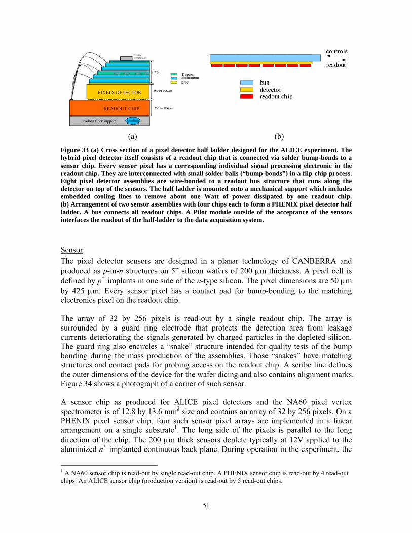
51
(a) (b)
Figure 33 (a) Cross section of a pixel detector half ladder designed for the ALICE experiment. The hybrid pixel detector itself consists of a readout chip that is connected via solder bump-bonds to a sensor chip. Every sensor pixel has a corresponding individual signal processing electronic in the readout chip. They are interconnected with small solder balls (“bump-bonds”) in a flip-chip process. Eight pixel detector assemblies are wire-bonded to a readout bus structure that runs along the detector on top of the sensors. The half ladder is mounted onto a mechanical support which includes embedded cooling lines to remove about one Watt of power dissipated by one readout chip. (b) Arrangement of two sensor assemblies with four chips each to form a PHENIX pixel detector half ladder. A bus connects all readout chips. A Pilot module outside of the acceptance of the sensors interfaces the readout of the half-ladder to the data acquisition system.
Sensor The pixel detector sensors are designed in a planar technology of CANBERRA and produced as p-in-n structures on 5” silicon wafers of 200 µm thickness. A pixel cell is defined by p+ implants in one side of the n-type silicon. The pixel dimensions are 50 µm by 425 µm. Every sensor pixel has a contact pad for bump-bonding to the matching electronics pixel on the readout chip. The array of 32 by 256 pixels is read-out by a single readout chip. The array is surrounded by a guard ring electrode that protects the detection area from leakage currents deteriorating the signals generated by charged particles in the depleted silicon. The guard ring also encircles a “snake” structure intended for quality tests of the bump bonding during the mass production of the assemblies. Those “snakes” have matching structures and contact pads for probing access on the readout chip. A scribe line defines the outer dimensions of the device for the wafer dicing and also contains alignment marks. Figure 34 shows a photograph of a corner of such sensor. A sensor chip as produced for ALICE pixel detectors and the NA60 pixel vertex spectrometer is of 12.8 by 13.6 mm2 size and contains an array of 32 by 256 pixels. On a PHENIX pixel sensor chip, four such sensor pixel arrays are implemented in a linear arrangement on a single substrate1. The long side of the pixels is parallel to the long direction of the chip. The 200 µm thick sensors deplete typically at 12V applied to the aluminized n+ implanted continuous back plane. During operation in the experiment, the
1 A NA60 sensor chip is read-out by single read-out chip. A PHENIX sensor chip is read-out by 4 read-out chips. An ALICE sensor chip (production version) is read-out by 5 read-out chips.

52
sensors are over-biased. The leakage currents are as low as a few nA in well diced material but can go up to a few µA without any danger to the sensors’ functionality. Nine PHENIX sensor ladders with four pixel arrays each are arranged on the production mask of a 5” wafer as shown in Figure 35. Diodes are placed in the remaining space. They are production-specific to the CANBERRA technology and serve the quality survey.
Figure 34 Photograph of a corner of a pixel detector sensor chip, seen through a microscope. A guard electrode surrounds the array of pixel implants. The scribe line defines the outer dimensions of the die.
Figure 35 Layout of a 5” silicon sensor wafer with nine PHENIX pixel sensor ladders.

53
Six sensor wafers with a total number of 54 ladders are ordered and will be delivered by the end of July 2004. This production covers the material for the 1st pixel detector layer. A second production batch to produce the sensor wafers for the 2nd pixel detector layer is planned for early September 2004.
Readout chip The pixel detector front-end electronics (“readout chip”) results from a research and development effort at CERN that started more than a decade ago28. The recent chip “ALICE1LHCb” is a mixed analog-digital ASIC designed in CERN's EP-MIC group and the ALICE and LHCb teams for an application in the Silicon Pixel Detector of the ALICE experiment and the RICH photo detection of the LHCb experiment at the LHC29. It is also being applied in the vertex spectrometer of the NA60 experiment at the SPS30. The chip is designed in a 0.25 µm process with radiation tolerant design layout techniques. Each chip has 32 by 256 pixels of 50 µm by 425 µm size. It is designed to be bump-bonded with solder balls of about 20 µm diameter to a silicon sensor that contains an array of sensor pixels with matching size and pitch. The chip provides a binary output signal for every pixel that indicates a charge release by a traversing particle. The threshold of the pixels' discriminators and various other parameters of the front-end electronics can be adjusted and programmed individually for every pixel. Each ALICE1LHCb chip is readout by clocking out 256 32-bit words at a frequency of 10 MHz. Every chip provides an “OR” signal of hit pixels for each readout clock cycle. This feature will allow us to utilize the pixel detector for the first-level trigger logic. A semi-automatic wafer probe station (model SÜSS PA200) has been installed by RIKEN at CERN for the quality assurance tests of the readout chips on the wafers. The station is fully operational. The picture of the probe station and a photograph taken during the ongoing quality assurance tests are shown in Figure 36.
Figure 36 Left: Picture of the wafer probe station installed at CERN for the quality assurance tests of the pixel readout chips. Right: Quality assurance test of ALICE1LHCb readout chips in a clean room laboratory at CERN.
The tests performed on the chips include an evaluation of the analog and digital power consumptions, the functionality of the analog and digital controls, and the minimum threshold and noise obtained in response to electrical test signals. Tests of the OR trigger

54
output are included as well. The chips are sorted into three quality classes (I – excellent, II – good, III- bad). Class-I chips are used for the production of the pixel detector ladders. A typical class map of a readout chip wafer is shown in Figure 37.
Figure 37 A typical class map of the readout chip wafer.
Four readout chip wafers with a total number of 344 chips have been probed so far, out of which 134 class-I chips were obtained. Detail numbers are shown in Table 7. The yield of class-I chips from the four tested PHENIX wafers is consistent with the results obtained by the ALICE pixel detector group. The mean minimum threshold and noise distributions for all class-I chips are shown in Figure 38.
Table 7 Yield of class-I, class-II and class-III chips from four probed wafers.
Wafer ID Class-I Class-II Class-IIIABA4J4T 36 14 36AAA4J5T 35 9 42A9A4J6T 25 13 48AVA4LLT 38 23 26
Total 134 59 152 The mean minimum thresholds of all 134 class-I chips is 1348 e- and the width is 300 e-
r.m.s. The mean noise is found to be 118 e- with 2.9 e- r.m.s. For single pixel hits the average sensor signal from minimum ionizing particles in 200 µm Si is about 16 000 e- so that a superb signal-to-noise ratio and particle detection efficiency is achieved.

55
Figure 38 Mean threshold and noise of 134 class-I ALICE1LHCb chips.
Sixteen readout chip wafers have been purchased and delivered. Based on the current yields, we expect about 500 to 540 class-I chips on those wafers. For the two layers of the silicon pixel detector, we are going to produce 150 4-chip ladders including spares. Those require a total number of 600 class-I chips. Additional wafers for the missing chips are available through ALICE. According to our experience, we spend about one week for a complete quality assurance test of one full readout wafer. We estimate that we will be able to complete chip probing for the inner two silicon pixel detector layers by the end of November 2004.
Interconnection of Sensor and Readout Chip (“Bump Bonding”) The term “bump-bonding” denotes the micro-interconnection of electrical structures with small “balls” of metals or alloys. It is essential for the construction of modern hybrid structures with two-dimensional arrays of high-density designs. Bump-bonding and flip-chip interconnection techniques were already introduced in the late 1960s. They became commercially available only about 15 years ago. Bonding with dimensions smaller than approximately 50 µm is still offered by only a rather small number of vendors or specialized laboratories, and becomes challenging at below 20 µm for specialized applications. The Technical Research Centre of Finland (VTT), Microelectronics Department of the Information Technology Division, is the vendor of choice at CERN for the production of flip-chip assembled pixel detectors for the ALICE and LHCb experiments. VTT offers an integrated package of bump-bond deposition, wafer thinning and flip-chip bonding31. Key features of the process are:

56
• 200-mm (8'') wafer capability. • Tin-lead solder alloy bumps are used for mechanical strength of the bonded
assemblies. • Bump deposition by electroplating. • Optional thinning (back grinding) of bumped readout wafers from native
thickness of 750 µm down to 150 µm. • Clean dicing with front side protection using either photo resist or tape. • Flux-less flip-chip bonding. Alignment accuracy better than 3µm. • Bump size down to smaller than 20µm diameter. • Throughput 3-4 assembly bondings per hour.
Statistics from the production of bump-bonded assemblies for the NA60 pixel vertex spectrometer in the year 2003, with chips of 750 µm and sensors of 300 µm thickness, and from the pre-production of thin ladders for the ALICE pixel detector illustrate that the industrial process of VTT is able to produce good yield for 20 µm bump bonds. In 2003, a grand total of 132 single-chip pixel detector assemblies were produced in multiple batches for NA60 at VTT. Out of those, 115 assemblies passed the acceptance test, i.e. had less than 1 % dead or noisy pixels. An example is shown in Figure 39. The average yield of accepted assemblies was 87 %. Several large batches, especially towards the end of the production, had a significantly higher yield than this average and reached even 100 % of accepted assemblies. In the same process, first pixel sensor assemblies were successfully produced for the ALICE experiment. Each of the assemblies contains five readout chips placed on a silicon sensor substrate of about 14 mm by 70 mm size that has five matching sensor pixel arrays implemented. The processing included the thinning of the readout chips to 150 µm before they were bump-bonded to the sensor.
(a) (b) (c)
Figure 39 Test result of a typical high-quality ALICE1LHCb assembly for the NA60 experiment: (a) Test pulse injection into the readout chip: 8 out of 8192 pixels are dead, the rest of the pixel array responds. (b) Source measurement with Sr90 to test the bump bonding quality: 3 out of 8192 bonds are open (or pixels do not respond electrically). (c) Image of a beta source with the shadow of the depletion voltage contact needle on the silicon sensor.
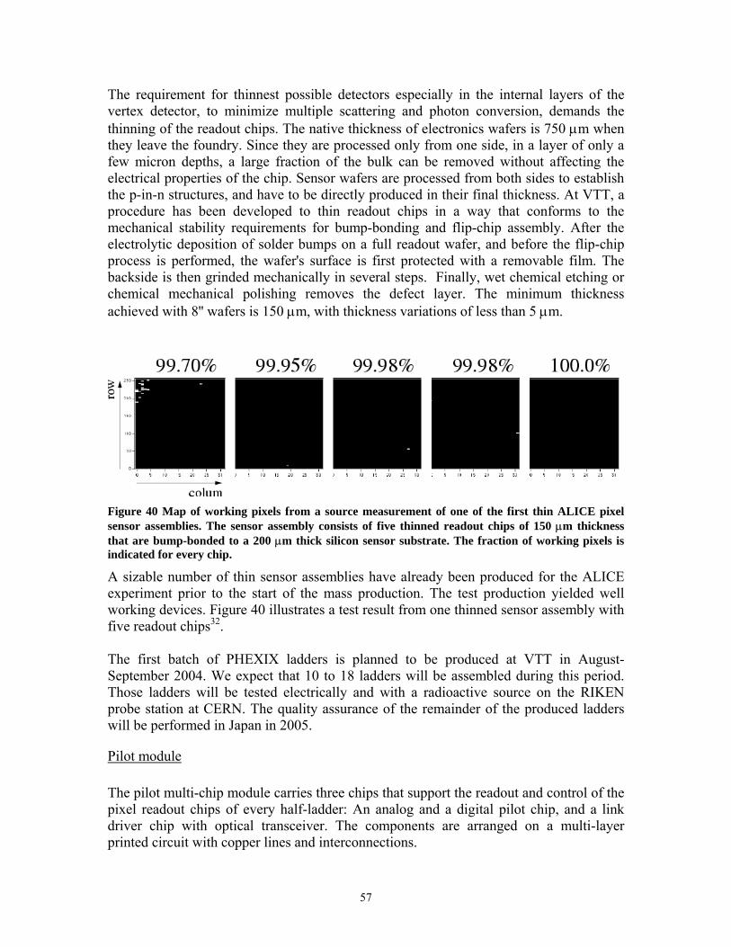
57
The requirement for thinnest possible detectors especially in the internal layers of the vertex detector, to minimize multiple scattering and photon conversion, demands the thinning of the readout chips. The native thickness of electronics wafers is 750 µm when they leave the foundry. Since they are processed only from one side, in a layer of only a few micron depths, a large fraction of the bulk can be removed without affecting the electrical properties of the chip. Sensor wafers are processed from both sides to establish the p-in-n structures, and have to be directly produced in their final thickness. At VTT, a procedure has been developed to thin readout chips in a way that conforms to the mechanical stability requirements for bump-bonding and flip-chip assembly. After the electrolytic deposition of solder bumps on a full readout wafer, and before the flip-chip process is performed, the wafer's surface is first protected with a removable film. The backside is then grinded mechanically in several steps. Finally, wet chemical etching or chemical mechanical polishing removes the defect layer. The minimum thickness achieved with 8'' wafers is 150 µm, with thickness variations of less than 5 µm.
Figure 40 Map of working pixels from a source measurement of one of the first thin ALICE pixel sensor assemblies. The sensor assembly consists of five thinned readout chips of 150 µm thickness that are bump-bonded to a 200 µm thick silicon sensor substrate. The fraction of working pixels is indicated for every chip.
A sizable number of thin sensor assemblies have already been produced for the ALICE experiment prior to the start of the mass production. The test production yielded well working devices. Figure 40 illustrates a test result from one thinned sensor assembly with five readout chips32. The first batch of PHEXIX ladders is planned to be produced at VTT in August-September 2004. We expect that 10 to 18 ladders will be assembled during this period. Those ladders will be tested electrically and with a radioactive source on the RIKEN probe station at CERN. The quality assurance of the remainder of the produced ladders will be performed in Japan in 2005.
Pilot module The pilot multi-chip module carries three chips that support the readout and control of the pixel readout chips of every half-ladder: An analog and a digital pilot chip, and a link driver chip with optical transceiver. The components are arranged on a multi-layer printed circuit with copper lines and interconnections.

58
The key component on the Pilot module is the digital pilot chip. The role of the digital Pilot is to read the data from the ALICE1LHCb chips. Upon pixel chip readout being initialized, each ALICE1LHCb presents 256 sequential words of pixel data on a 32-bit bus synchronously at a 10MHz clock. Thus, 25.6µs is required to read the data from a single chip. In the PHENIX data acquisition system, the readout is ultimately performed in 40µs to achieve a maximum throughput of 25 kHz. A sequential readout of the eight chips on two half ladders requires 204µs to empty the pixel chip data into the pilot, and hence does not meet our timing constraints. To satisfy the readout time requirement of PHENIX, we must readout for pixel chips in parallel, thus 4×32-bit data will be transmitted to the Pilot module. We are currently investigating several options of the Pilot module design to handle four times more data bits than the ALICE Silicon Pixel Detector has.
Figure 41 A first version of the modified digital pilot chip which handles 2×32 bit data inputs has been submitted as part of a multi project wafer at CERN to IBM in May 2004.
One solution could be to read out each of the parallel branches with one of the existing ALICE pilot ASICs. Since in the PHENIX vertex detector environment free space is available between the end-cap detectors and the magnet poles (“nose cones”), unlike in the extremely tight ALICE Inner Tracker region, such a solution with multiple ALICE pilot chips can be considered. It would require about four times the space of an ALICE pixel Pilot module (external dimensions: about 80 mm by 13.8 mm), and also four times

59
more optical fiber lines to read or control data from the half ladder. For the ALICE design, three fibers (clock, control, data link) are connecting to the Pilot module. The other solution is based on a new pilot ASIC. This ASIC option uses the same design rules and radiation tolerant technology as the Pilot ASIC that is presently already functional. This option requires only twice the space of the present design of the ALICE pixel Pilot module, and twice the number of optical fibers. A first version of the modified digital Pilot chip which handles 2×32 bit data inputs has been submitted as part of a multi project wafer at CERN to IBM in May 2004. The design is shown in Figure 41. The modification is rather straight forward. Therefore, we expect to have a functional new Pilot chip ASIC from this submission. However, we are also preparing for the submission of another version in November 2004 if necessary. The data transmission from the readout chip to the pilot chip is performed in the following way. The bus carries two times 32 bits with a frequency of 10 MHz to the Pilot chip. The Pilot chip is designed to output at 40 MHz. This means that four 25 ns transmission cycles are available before the next data word from the readout chips arrives. The first two clock cycles are referred to as “cycle-0” and the last two clock cycles as “cycle-1”. If no pixel data readout is performed, only control data which includes the fast-OR signals is transmitted in the cycle-0. The fast-OR signal can be used to generate a LVL1 trigger, which is discussed in section 3.5. These data is referred to as slot-0. In this case cycle-1 contains only empty data. During pixel data readout, after transmission of the data of slot-0, event header information (slot-1a) is transmitted in cycle-1.This is followed by repeated slot-0 and slot-1b which contain the pixel hit information. The principle of the data transmission is illustrated in Figure 42.
Figure 42 Illustration of the data transmission from the pixel detector.
Readout Bus The Pixel bus is a printed circuit sandwich made from Kapton and aluminum/copper layers to provide power and control signals for the pixel readout chips, and to bring signals out to the Pixel pilot module. The connections between the readout chips and the pixel bus are made by wire-bonding. Therefore the metal layers are arranged in vertical steps along the long side of the bus. The pixel bus will be 1.4 cm wide and about 40 cm long. At the end of the bus the pilot modules are placed. In the current design, the pixel bus is composed of five metal layers: ground, power, signal lines and a layer for detector bias and auxiliary passive components. The cross section of the pixel bus is seen in Figure 43.

60
“Horizontal” lines on one component of the signal double-layer are running parallel with the long direction of the pixel bus to rout the signals to the Pilot module. “Vertical” lines on the other component are connected to bond pads on the side of the bus for the wire-bonding to the readout chips. Through-hole connections between the horizontal and vertical lines interconnect the two signal layer components. Since four ALICE1LHCb chips must be read out in parallel to meet the PHENIX timing requirement, 190 signal and control lines are needed in the horizontal layer, which corresponds to 70 µm line pitch in a single signal layer as seen in Figure 43(a). The capabilities of industrial partners are being explored for a production of such fine pitch aluminum lines. On the other hand, technology to for lines with 60 µm pitch in a copper layer is commercially available. For this reason, a five-layer pixel bus with copper lines for the horizontal and vertical layers, and other lines made from aluminum will be our back-up solution. The material budget for the back-up option will be 0.236 % radiation length. To make a further reduction of the material budget possible, the effort to produce a pixel bus with exclusively aluminum lines will be continued. Due to the technical challenge of producing 70 µm pitch aluminum lines, the addition of another signal layer in the pixel bus will be an option. The cross section of the pixel bus made exclusively from aluminum metal layers is seen in Figure 43(b). For this option, the signal line pitch will be 140 µm and the thickness for the pixel bus will be 0.139 % radiation length. The development of a fine pitch pixel bus made from Al-Kapton layers is conducted in cooperation with a company in Japan. One of the most challenging steps is the production of the fine pitch aluminum traces by etching. Figure 44 shows the results from a first test production with line widths of 40 µm at 120 µm pitch. The further development toward the PHENIX pixel bus production is in progress.
Figure 43 Cross section of the structure of the pixel bus. Two technical solutions are being investigated. Option (a) contains a high-density double-layer of signal lines with a mean line pitch of 70 µm. Option (b) uses a reduced line-density on two signal double-layers with an average line pitch of 140 µm.

61
Figure 44 Aluminum traces on a Kapton substrate from a first test production for the PHENIX pixel bus.
Front End Modules The Pilot module transmits its data via optical fiber. A Front-End Module (FEM) will communicate with the Pilot module on one side, and the PHENIX DAQ and slow control system on the other side. Since the Pilot module transmits the data via optical fiber, the FEM can be located in electronic racks away from the vertex region. Each FEM may receive data from several pixel half ladders and thus reduce the number of Data Collection Modules (DCM) needed to interface to the PHENIX DAQ. In order to allow simple manipulations of the data, the FEM will pipe the data through an FPGA. This FPGA will add data headers and trails to for standard PHENIX data packages. Optionally the data may be further zero suppressed at the bit-level at this stage to reduce the data volume that need to be transferred. The design of the FEM is very similar to FEM's that are currently employed in the PHENIX readout system. Assembly of pixel detector ladders and the barrel detector layer: The assembly of the pixel detector modules will be performed in a two-step procedure that yields half-ladders and is outlined here. All components that go into the assembly (sensor ladders, pixel bus, Pilot module, power cable) have passed specific quality acceptance tests. The detailed procedure of the detector layer assembly is still to be defined. In the first step, the two sensor ladders are geometrically aligned on an assembly fixture, with the sensors facing up. Glue is deposited on the sensors. The pixel readout bus is then aligned with respect to the sensor ladders and brought into contact with the glue. It is important that especially the area under the bond pads of the pixel bus is properly glued, in order to yield mechanical stability for the wire-bonding. The glue must be electrically insulating and elastic enough to reduce mechanical stress that occurs with temperature cycling during the operation of the pixel detector, even when cooled through the fixture. Due to the fragility of the sensor ladders, no pressure can be applied during the gluing process. The curing temperature must be low enough to exclude damage to the solder bump bonds. A power cable and the Pilot module in about 40 cm distance at the other end

62
of the pixel bus can be glued in a similar way with the corresponding contact pads of the components aligned. In the second step, the readout chips and the pixel bus are interconnected through wire-bonding. Also the sensor bias connection and the interconnections between pixel bus and pilot module are established. Finally, the fully assembled and tested pixel detector half-ladders will be mounted onto the VTX barrel support. Our current model of this procedure utilizes a tool that lifts the half-ladders from their assembly fixtures and places them in their final positions. On the barrel support, thin aluminum grounding foils are already installed, which establish a well-defined electrical potential to the back side (bulk) of the pixel readout chips. The glue between pixel chips and grounding foil is therefore required to be electrically conductive. It must also provide good thermal conductivity for the heat transfer to the cooling system that is embedded in the mechanical support. Since no mechanical pressure can be applied, a candidate technology is glue that hardens quickly under exposure with UV light that is emitted from a light guiding tool at the side of the ladder once the final contact between ladder and support has been established. Electrically insulating glue with good thermal conductivity and adhesion to the support material is required between the grounding foil and the barrel support.
Pixel detectors operating in the NA60 experiment: Hybrid pixel detectors as described above are already being applied in the NA60 experiment at the SPS at CERN. NA60 studies the production of open charm and prompt dimuons in collisions induced by proton and heavy ion beams on nuclear targets. For this task, several novel detector systems were added to the dimuon spectrometer and zero-degree calorimeter, which were previously used in the NA50 experiment. The main upgrade is a new silicon pixel vertex spectrometer, which contains a tracking telescope, shown in Figure 45. The vertex spectrometer is built from ALICE1LHCb pixel detectors. Ninety-six single-chip pixel assemblies are arranged on 16 tracking planes with 4 or 8 chips that are operated on pixel busses on ceramic substrates. The readout electronics utilizes the pilot prototype chip that was developed for the ALICE Pixel Detector, and the driver chip developed at CERN for the optical link. In the year 2002, during the construction phase of the NA60 pixel detector modules, a sub-set of three tracking planes was operated in the experiment and used to track particles in low-energy Pb-Pb collisions. The run confirmed the feasibility of the detector concept in both technical aspects of the module construction and the vertex reconstruction performance33. One half of the telescope was then characterized in a test beam run in September 2003. The full telescope with 16 detector planes was installed and operational in the NA60 experiment during the physics run with high-energy Indium beams in Fall 2003 (Figure 46). The full readout chain has been working well in the NA60 data acquisition system.

63
Figure 45 The vertex spectrometer of the NA60 experiment comprises a 16-plane pixel detector telescope mounted in a 2.5 T dipole magnetic field in 7 cm to 32 cm distance downstream of the targets. Every plane is built from four or eight ALICE1LHCb single-chip pixel detector assemblies, which are mounted on ceramic printed circuit boards.
Figure 46 Average-multiplicity event in collisions of a 158 AGeV/c Indium beam with a segmented Indium target, reconstructed with 16 pixel detector planes during the physics run of NA60 in Fall 2003.
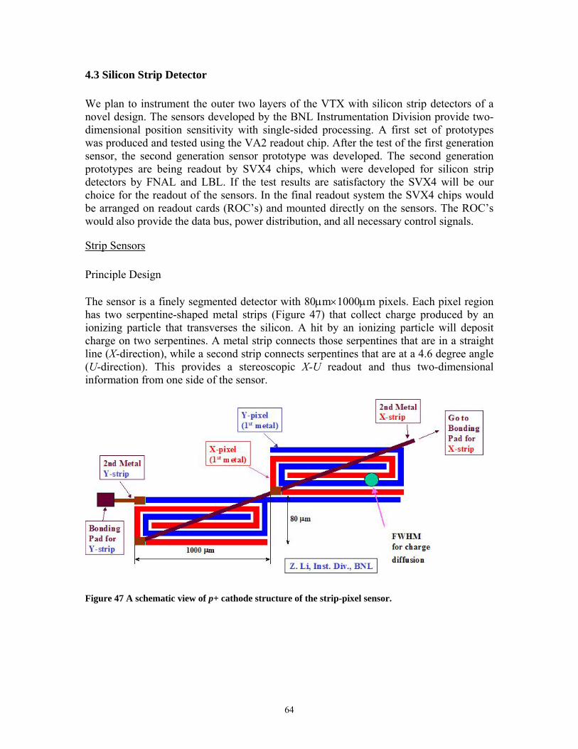
64
4.3 Silicon Strip Detector We plan to instrument the outer two layers of the VTX with silicon strip detectors of a novel design. The sensors developed by the BNL Instrumentation Division provide two-dimensional position sensitivity with single-sided processing. A first set of prototypes was produced and tested using the VA2 readout chip. After the test of the first generation sensor, the second generation sensor prototype was developed. The second generation prototypes are being readout by SVX4 chips, which were developed for silicon strip detectors by FNAL and LBL. If the test results are satisfactory the SVX4 will be our choice for the readout of the sensors. In the final readout system the SVX4 chips would be arranged on readout cards (ROC’s) and mounted directly on the sensors. The ROC’s would also provide the data bus, power distribution, and all necessary control signals.
Strip Sensors Principle Design The sensor is a finely segmented detector with 80µm×1000µm pixels. Each pixel region has two serpentine-shaped metal strips (Figure 47) that collect charge produced by an ionizing particle that transverses the silicon. A hit by an ionizing particle will deposit charge on two serpentines. A metal strip connects those serpentines that are in a straight line (X-direction), while a second strip connects serpentines that are at a 4.6 degree angle (U-direction). This provides a stereoscopic X-U readout and thus two-dimensional information from one side of the sensor.
Figure 47 A schematic view of p+ cathode structure of the strip-pixel sensor.

65
Figure 48 A schematic view of the prototype silicon strip sensor.
Figure 48 shows a schematic view of the prototype strip sensors and their geometrical dimensions. The total size of the sensor is 34.3mm×64.6mm. Each sensor is divided into two sides of separate sensitive areas with a dimension of 30.7mm×30.0mm. The active areas are segmented into pixels of 80µm×1000µm, which are connected to X- and U-strips as discussed above. Each strip sensor has a total of 1536 channels, 2×384 channels per side, half of them in X- and the other half in U-direction. First prototypes where produced with 250 and 400 µm thickness. These detectors have been tested in the laboratory and in beam. The second generation of prototypes with 400 and 500 µm thickness have been developed and are being tested their performance as this document is being prepared.
Laboratory tests of the strip sensors The initial tests of the prototype sensors have shown good results. Figure 49 shows the measured current and capacitance as a function of the bias voltage. Full depletion is

66
achieved at a bias voltage of ~80 V. At this voltage the capacitance of each strip is ~10 pF and the leakage current is less than 10 nA. To test the sensors in more detail, the Instrumentation Division in BNL has constructed a laser test setup. During the R&D phase the laser setup allows to studies of the properties of the sensors and to find the optimum operation condition, which includes the depletion voltage, the charge collection efficiency, the response to the carrier drift process, electric field profile inside the sensor and so on. The transient current technique (TCT)34 [1] is applied to obtain the electrical properties of the sensors. The technique is based on the analysis of the current and/or charge pulse shapes, which arise from electron-hole pairs created inside the detector by injecting the fast laser light. During the mass production of sensors, the existing setup or a newly developed setup based on our experience will provide the basic tool for quality control of the strip sensors and later of the assembled detector ladders.
Figure 49 Current and capacity characteristics of a prototype sensor.
Figure 50 shows the schematic layout of the laser test setup. The picture of the laser test setup is shown in Figure 51. A nano-second pulsed laser coupled into a focuser through an optical fiber is operated with a pulse generator. Two types of laser are used in the laser tests. One is a red laser with the wavelength of 635 nm and the penetration depth of 3 µm in silicon, and the other is an infrared laser with the wavelength of 1060 nm and the penetration depth of 800 µm in silicon. The red laser is used to study the separate collection of electrons and holes. The infrared laser is used to study the response of the detector to the charge deposition of a minimum ionizing particle (MIP). The focuser was fixed to a XYZ motorized stage. The precision of the laser spot positioning with the motorized stage is 0.5 µm. The laser spot size achieved after focusing is about 10µm in diameter. The current laser test setup is controlled with manual controllers and will be upgraded to have an automatic control with a LabVIEW compatible multi-axis motor drive.
1nA
0.1 1 10 100 500
Bias voltage (V)
10 |-5
10 |-4
10 |-3
10 |-2
10 |-1
10 |0
Cur
rent
(uA
)
0.1 1 10 100 500
Bias voltage (V)
10 |-5
10 |-4
10 |-3
10 |-2
10 |-1
10 |0
Cur
rent
(uA
)
Strip Detector 1234-BY1, 400 um, 0.024 cm2/strip, 10 cm long
0.1 1 10 100 500
Bias voltage (V)
10 |1
10 |2
Cap
acita
nce
(pF)
Strip Detector 1234-BY1, 400 um, 0.024 cm2/strip, 10 cm long

67
Figure 50 Schematic layout of the laser test setup.
Figure 51 A laser test setup for the strip sensor.
Beam test of the first generation sensor proto-type The first generation proto-types sensors were tested using test beam at KEK. To test the prototypes in beam, the sensors were mounted on readout cards designed to read out signals from one side of the sensors (see Figure 52). Each plane consists of a silicon strip sensor, six readout chips, a base-board, two fan out boards (pitch adaptors) and two SMT boards. A bias voltage was applied in the sensor backplane (ohmic side) through the base-board. An analog multiplexer readout chip with 128-channel charge sensitive preamplifier-shaper circuits, VA2 chip of Ideas ASA35, was used to read out signals from the sensor. The preamplifier-shaper has a 1-3 µsec peaking time and a nominal gain of 30 mV/pC. The SMT board was designed to operate the VA2 chips and read out multiplexed analog signals through an interface with a VME data acquisition system. Three detectors planes with 400 µm thick sensors and four with 250 µm thick sensors were constructed.

68
Figure 52 A prototype detector using the first generation sensor.
The sensor performance in terms of charge sharing properties, detection efficiency and position resolution has been evaluated with a 90Sr β-source and in the test beam at KEK. The beam test was performed at T1 beam line in KEK-PS, which delivered a positively charged particle beam with momentum of 0.5 - 2.0 GeV/c. Charge sharing property in x-strip and u-strip can be characterized by the asymmetry, AQ = ( Qx - Qu ) / ( Qx + Qu ), where Qx and Qu represent collected charges in X-strip and in U-strip, respectively. For optimum two-dimensional position sensitivity, one expects that AQ on average is zero with a narrow width. The results of the AQ measurements are plotted in Figure 53. The source test shows the AQ distribution peaking at zero with a width of about 0.18. This demonstrates that the principle of two-dimensional position sensitivity by charge sharing works. In the beam tests AQ exhibited a dependence on the incident angle of the beam normal to the sensor surface, θinc. For θinc = 15 degrees and 30 degrees narrow distribution with a peak at zero were observed. However, at θinc = 0 degrees broad distributions which did not peak at zero were found. This deficiency was traced back to the line width (8µm) and gap spacing (5µm) of the p+ electrode structure in a single pixel. The line width is too wide compared with the size of charge diffusion, and therefore the charge sharing ratio of the X and the U strips depends on the position of the hit. For the second-generation prototype sensors a narrower line width (5µm) and gap spacing (3µm) was chosen to overcome this problem.
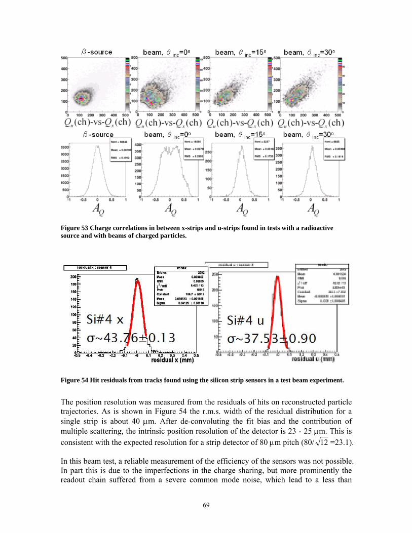
69
Figure 53 Charge correlations in between x-strips and u-strips found in tests with a radioactive source and with beams of charged particles.
Figure 54 Hit residuals from tracks found using the silicon strip sensors in a test beam experiment.
The position resolution was measured from the residuals of hits on reconstructed particle trajectories. As is shown in Figure 54 the r.m.s. width of the residual distribution for a single strip is about 40 µm. After de-convoluting the fit bias and the contribution of multiple scattering, the intrinsic position resolution of the detector is 23 - 25 µm. This is consistent with the expected resolution for a strip detector of 80 µm pitch (80/ 12 =23.1). In this beam test, a reliable measurement of the efficiency of the sensors was not possible. In part this is due to the imperfections in the charge sharing, but more prominently the readout chain suffered from a severe common mode noise, which lead to a less than

70
expected signal-to-noise ratio. This prohibited an efficient hit detection. At present only the lower limits for the efficiency can be quoted. They are 98%, 96%, and 88% for three 400 µm thick sensors. The low efficiency, 88%, for one of the three test sensor can be attributed to electronic noise at the beam test. A similar study for the second generation sensors is underway. The detection efficiencies and the signal-to-noise ratios are under study and are expected to be improved by optimizing the operational condition of the detector and by introducing a more appropriate readout chain based on the SVX4 chip.
The Second Prototype Sensor and Tests with SVX4 Readout Chip The second prototype sensor was designed to have 5 µm line width and 3 µm gap spacing of the p+ electrode structure in a single pixel. The sensor is expected to have better charge-sharing property, compared with the first prototype sensor with 8 µm line width and 5 µm gap spacing. The second prototype sensor has been processed by the BNL Instrumentation Division. Four sensors with 400 µm and four with 500 µm thickness were fabricated by the end of January 2004 and the middle of May 2004, respectively. Detectors composed of the second prototype sensors and the electronics hybrids with the SVX4 readout chips were constructed. The study of the signal-to-noise ratio in the detector is essential for the strip detector development and is under way. The design of the detector is similar to the first prototype detector shown in Figure 52. The VA2 chips and the SMT board in the first prototype detector have been replaced with the electronics hybrid shown in Figure 56, which is developed for CDF Run-IIb Silicon Detector. Three of the four SVX4 chips mounted on the hybrid are used to readout 384 X- or U-strips of the sensor. One hybrid received from the CDF collaboration is used for the detector. The hybrid is operated by using a test board, which is a simplified version of the PHENIX DAQ.
New Sensor Design We have developed an improved design of the strip-pixel sensor, which matches the strip ladder detector design including the ROC described below. Major changes compared with the 1st and 2nd prototypes are : 1) Readout pads are located in the longer-edge of the sensor to make a room for RCC in the center of the sensor and for bus connections between ROCs. This change can be done in the 2nd aluminum layer. 2) Dead space of the 30 U-strips in the upper-side in Figure 48 is eliminated by connecting those U-strips to the U-strips in the lower-side in Figure 48. This change also can be done in the 2nd aluminum layer. 3) Dead space in the middle of the sensor is eliminated. 4) Aluminum lines connected to the inner guard ring are added around the readout pads to make the sensor tests easier. The modified design developed with Hamamatsu is shown in

71
Figure 55. The strip-pixel structure of 80 µm × 1000 µm pixel with 5 µm width and 3 µm gap p+ line was kept.
Figure 55 The new design of the strip-pixel sensor.

72
The production of sensors with this improved design will be done by Hamamatsu as a part of the pre-production process described below. The new sensor will be delivered by the end of September, 2004.
Sensor pre-production The mass production of the strip-pixel sensor will be done at a company. Key technologies for the strip-pixel sensor production are to make very fine p+ pattern (5µm width and 3µm gap) and to do the double-metal process. In order to evaluate the mass production capability of the (strip-pixel sensor) companies, we recently submitted pre-productions of the sensors to two candidates: SINTEF in Norway and Hamamatsu (HPK) in Japan. Both companies have an excellent experience in processing silicon detectors for large-scale experiments. The sensor design for the pre-production at SINTEF is the same as that of the 2nd prototype sensor. The wafer layout in SINTEF includes two sensors on one 4” wafer. The thickness is 500µm. We submitted the process for 40 sensors in the middle of May, 2004. The pre-production in SINTEF is under way. The pre-production sensors will be delivered around the middle of August. The sensor design for the pre-production at HPK is of two types. One is the same as that of the 2nd prototype and the other is the new design described above. The wafer layout in the HPK includes three sensors on one 6” wafer. Our plan is to submit the process for 20 sensors including both designs. The thickness is 625 µm or 500µm. The pre-production in HPK will be submitted soon and will be delivered by the end of September.
SVX4 readout chip The strips will be read out with the SVX4 chip developed by FNAL/Berkeley collaboration. The SVX4 is implemented in the 0.25 µm TSMC process and is inherently rad-hard. It is a 128-channel chip with a 46-deep pipeline cycled by the beam-crossing clock, thus providing the LVL1-latency required by the PHENIX DAQ. LVL1-accepted events are stored for future pipelined readout. The SVX4 allows up to 8 bits of analog information, although the number of bits are programmable. Several pedestal-subtraction steps offer robust protection against common-mode noise. On-board zero suppression is provided for, but can be turned off (see discussion below). The SVX4 also provides for four-deep multi-event buffering required by the PHENIX DAQ. FNAL has a complete wafer-testing station and has indicated a willingness to take on the required wafer testing of our chips. A test board has been developed at ORNL that has allowed us to verify compatibility of the SVX4 with the PHENIX DAQ (serial programming, clock & fast control and data read-out). In fall 2003 FNAL cancelled the Tevatron Run-IIb silicon upgrade projects. There are already sufficient SVX4 chips that have been produced to meet our needs. We are in negotiations with FNAL for the purchase of these chips. In the present plan, we will

73
purchase 18 wafers of the SVX4 chip, which should produce about 5,000 good chips (based on the measured good chip yield), giving us what we require plus adequate spares.
Sensor Readout Card (ROC) / Readout Bus CDF has implemented readout of a silicon detector using 2cm x 4cm circuit boards holding four SVX4 chips operating in a daisy-chain mode to reduce signal bus requirements, see Figure 56. We have chosen a similar implementation, but we require twelve SVX4 chips in a 3cm x 6cm area to readout both orientations (1536 channels) of a sensor. Using a nomenclature common to a number of other PHENIX subsystems the circuit boards hosting the SVX4s are termed Readout Cards (ROC’s). There is one ROC per sensor, 5 (layer 3) or 6 (layer 4) sensors per ladder and 44 ladders for a total of 246 ROC’s (and 2952 SVX4s).
40 mm
28 mm
Signal inputs wire-bonded to sensors.
40 mm
28 mm
Signal inputs wire-bonded to sensors.
Figure 56: CDF Hybrid with dimensions shown. This board contains four SVX4 chips, local power filtering and traces for power, ground and data/control signals and is functionally equivalent to the proposed ROC.
In addition to twelve SVX4s, each ROC has one custom, digital ASIC (or perhaps a rad-hard FPGA), known as the ROC Control Chip (RCC). The technology choice between an ASIC or a rad-hard FPGA will be made based on radiation dose measurements and space constraints. Since these chips are purely digital they can be completely tested inside an FPGA implementation (greatly simplifying any necessary revisions) and a technology choice can be postponed. The RCCs are relatively simple, with a block diagram shown in Figure 57, below. They effectively serve as a state-driven de-multiplexer, directing the serial and clock & fast control inputs and the data outputs, depending on the SVX4 state selected (Initialize, Digitize or Readout) and on the geographical address of the ROC. They also hold digitized data awaiting readout (the SVX4 itself buffers four un-digitized events tagged with a Level-1 accept signal). The SVX4 cannot read out one event and digitize another

74
at the same time. But, in order to conform to the PHENIX DAQ requirements, the system must be prepared to be read out a second event immediately after a prior event is read out. The RCC is therefore required as a buffer to hold data read out from the SVX4s immediately after digitization so that they will be prepared to read out a second event by the time the entire ladder is read out. Furthermore, it also serves to minimize the effects of single-point failures (one broken SVX4 could take out all of the chips in its serial path). In from Pilot:BECLKPRD1PRD2PARSTL1ACHMODEBEMODEFEMODEFECLKPRI-INCALSTRBCOMPRSTRREFSELRAMPRSTENDDATINIT_RESETRESYNC_RESET4XBCLK
Out to SVX4:BECLKPRD1PRD2PARSTL1ACHMODEBEMODEFEMODEFECLKPRI-INCALSTRBCOMPRSTRREFSELRAMPRST
In from board:CHIP IDENDDAT_LOC_INROERR_IN(2)
In from SVX4:PRI-OUTOBDVDATABUS (8)
Out to Pilot:SCLKPRI-OUTOBDVDATABUS (8)
Out to board:ENDDAT_LOC_OUTROERR_OUT(2)
Chip Selected?
Mode = Initialize?
Mode = Digitize?
Mode = Readout?BufferFIFO
Data Xfer
BCLK Count
L1AINIT_RESETRESYNC_RESET4XBCLK
In from Pilot:BECLKPRD1PRD2PARSTL1ACHMODEBEMODEFEMODEFECLKPRI-INCALSTRBCOMPRSTRREFSELRAMPRSTENDDATINIT_RESETRESYNC_RESET4XBCLK
Out to SVX4:BECLKPRD1PRD2PARSTL1ACHMODEBEMODEFEMODEFECLKPRI-INCALSTRBCOMPRSTRREFSELRAMPRST
In from board:CHIP IDENDDAT_LOC_INROERR_IN(2)
In from SVX4:PRI-OUTOBDVDATABUS (8)
Out to Pilot:SCLKPRI-OUTOBDVDATABUS (8)
Out to board:ENDDAT_LOC_OUTROERR_OUT(2)
Chip Selected?Chip Selected?
Mode = Initialize?
Mode = Digitize?
Mode = Readout?BufferFIFO
Data Xfer
BCLK Count
L1AINIT_RESETRESYNC_RESET4XBCLK
Figure 57: RCC block diagram. This chip, implemented as either a rad-hard FPGA or a fully digital ASIC, serves primarily as a simple, state-driven de-multiplexer. Additionally, a FIFO is used to buffer digitized data allowing simultaneous digitization and readout.
The simplicity of this chip has two important consequences: 1) The chip’s size will likely be determined by the required number of I/O pins (~ 50 signals, primarily differential LVDS), with 5mm x 5mm likely to be sufficient. 2) If expected dose or space limitations require the use of an ASIC we expect it to be relatively straightforward to convert from the FPGA implementation to an ASIC, although the layout of an ASIC version would need to take the radiation environment into account. The SVX4 chip is designed for the use with an AC-coupled strip sensor but the strip-pixel sensor is a DC-coupled device. There are three consequences of the difference in coupling. The first is that the leakage current from the sensor will rapidly saturate the SVX4 input preamp. The preamp dynamic range is 200 fC, which will saturate in 20 µsec with a nominal 10 nA leakage current. However, we can issue a preamp-reset signal once

75
per RHIC abort gap (~13 µsec) allowing a hit rate per strip-pixel of ~2MHz before saturating between resets. The leakage current also increases the system noise. However, the SVX4 uses correlated sampling, measuring the pedestal on the first quarter of every clock cycle and the signal on the remaining three-quarters of the cycle. Therefore the noise increase is only due to the jitter on the injected electrons over a single 106 nsec cycle (√6000 electrons ~ 80 electrons) which is less than 0.1% of the expected signal size. Finally, at room temperature the leakage current temperature is highly temperature dependent, which could result in significant time-dependent pedestal shifts. All these problems are exacerbated by exposure of the sensor to radiation. The leakage current can be reduced by cooling the sensors, but explicit AC decoupling of the SVX4 and the sensor may be required. Sensor/SVX4 tests with and without external capacitive coupling will be made to test this conclusion by inserting SMD capacitors and resistors between the sensor and the SVX4 chip. Once the specification of the SMD components is fixed, we can transfer the specification to a small “RC” chip, matching the SVX4 pitch, which Hamamatsu has experience fabricating. The sensor design, which incorporates a pitch adapter directly into one of the metallization layers, eliminates the complication of an external pitch adapter. Since the ROC’s completely cover the sensor, and since they require ground-planes, power planes and control signal traces, we daisy-chain those contacts across the ROC boundaries to form a bus without any extra material. There is more than sufficient room for the ROC-to-ROC signal and power connections as shown in Figure 58, below. (Signal buses are shown to scale assuming 100/100 µm trace/space). This leaves nearly 2cm for power and ground connections. The implementation of this daisy-chain needs further evaluation.
SVX4X2
“RC Chip”
SVX4U1
“RC Chip”
SVX4U4
“RC Chip”
SVX4X3
“RC Chip”
SVX4X1
“RC Chip”
SVX4X6
“RC Chip”
SVX4U6
“RC Chip”
SVX4U5
“RC Chip”
SVX4U3
“RC Chip”
SVX4U2
“RC Chip”
SVX4X4
“RC Chip”
SVX4X5
“RC Chip”
RCC
Control signal daisy-chain
Data signal daisy-chain
Power daisy-chain
SVX4X2
“RC Chip”
SVX4X2
“RC Chip”
SVX4U1
“RC Chip”
SVX4U1
“RC Chip”
SVX4U4
“RC Chip”
SVX4U4
“RC Chip”
SVX4X3
“RC Chip”
SVX4X3
“RC Chip”
SVX4X1
“RC Chip”
SVX4X1
“RC Chip”
SVX4X6
“RC Chip”
SVX4X6
“RC Chip”
SVX4U6
“RC Chip”
SVX4U6
“RC Chip”
SVX4U5
“RC Chip”
SVX4U5
“RC Chip”
SVX4U3
“RC Chip”
SVX4U3
“RC Chip”
SVX4U2
“RC Chip”
SVX4U2
“RC Chip”
SVX4X4
“RC Chip”
SVX4X4
“RC Chip”
SVX4X5
“RC Chip”
SVX4X5
“RC Chip”
RCC
Control signal daisy-chain
Data signal daisy-chain
Power daisy-chain
Figure 58 ROC top layer w/ major components (SVX4, RCC) and bus connections shown. There are a relatively small number of additional passive components required, as shown in the CDF implementation in Figure 56. Two ROC’s read out one sensor, a total of eight are incorporated in one ladder. The figure is drawn to scale.

76
The primary trace count on the ROC’s is due to the connections from the ladder bus to the RCC and from the RCC to the SVX4s. A possible sketch of the trace layout (to scale) is shown in Figure 59, showing that two trace layers (in addition to some surface traces) should be sufficient.
Control Signal Bus
Data Signal Bus
Inner Trace Layer
RCC/SVX4 Bus
Control Signal Bus
Data Signal Bus
Inner Trace Layer
RCC/SVX4 Bus
Control signal daisy-chain
Data signal daisy-chain
Power daisy-chain
Control signal daisy-chain Control signal daisy-chain
Data signal daisy-chainData signal daisy-chain
Control signal ladder bus into RCC
Data signal ladder bus into RCC
SVX4 to RCC bus SVX4 to RCC bus
Top Trace Layer
Control signal daisy-chain
Data signal daisy-chain
Power daisy-chain
Control signal daisy-chain Control signal daisy-chain
Data signal daisy-chainData signal daisy-chain
Control signal ladder bus into RCC
Data signal ladder bus into RCC
SVX4 to RCC bus SVX4 to RCC busControl signal daisy-chain
Data signal daisy-chain
Power daisy-chain
Control signal daisy-chain Control signal daisy-chain
Data signal daisy-chainData signal daisy-chain
Control signal ladder bus into RCC
Data signal ladder bus into RCC
SVX4 to RCC bus SVX4 to RCC bus
Top Trace Layer
Control Signal Bus
Data Signal Bus
Inner Trace Layer
RCC/SVX4 Bus
Control Signal Bus
Data Signal Bus
Inner Trace Layer
RCC/SVX4 Bus
Control signal daisy-chain
Data signal daisy-chain
Power daisy-chain
Control signal daisy-chain Control signal daisy-chain
Data signal daisy-chainData signal daisy-chain
Control signal ladder bus into RCC
Data signal ladder bus into RCC
SVX4 to RCC bus SVX4 to RCC bus
Top Trace Layer
Control signal daisy-chain
Data signal daisy-chain
Power daisy-chain
Control signal daisy-chain Control signal daisy-chain
Data signal daisy-chainData signal daisy-chain
Control signal ladder bus into RCC
Data signal ladder bus into RCC
SVX4 to RCC bus SVX4 to RCC busControl signal daisy-chain
Data signal daisy-chain
Power daisy-chain
Control signal daisy-chain Control signal daisy-chain
Data signal daisy-chainData signal daisy-chain
Control signal ladder bus into RCC
Data signal ladder bus into RCC
SVX4 to RCC bus SVX4 to RCC bus
Top Trace Layer
Figure 59 ROC signal trace layers. The figure is drawn to scale with bus widths given with a 100/100 µm trace/spacing assumption.
Pilot Module The ROC’s need to receive timing and control signals and they need to send out data. The space available at the end of the ladders (2x3 cm) and the inaccessibility of this area both argue to put as little intelligence there as possible. Thus a pilot module, wire-bonded to the ROC bus at the end of each ladder will drive signals to a remote Front-End Module (FEM), described below. Signals may be driven off the Pilot Module either on copper (w/ e.g., the rad-hard LVDS transceiver developed by FNAL for this purpose for the CDF

77
Silicon detector; or by the RCCs themselves) or on fiber (with e.g., the Texas Instruments TLK1501, a very-low power 16-bit serializer/de-serializer chip plus an optical link, an option being considered for a number of LHC detectors). The fiber option is especially attractive (reduced cable plant, lack of electrical connection and consequent grounding concerns, and the ability to put the FEM’s in a truly remote location), but the feasibility of this option needs to be addressed further.
Front-End Module The Front-End Module (FEM) will serve as the interface between the ladders and the PHENIX DAQ (Serial Control (Arcnet), Clock & Control (Granule Timing Module), and the Data Collection Module). The FEM’s will be outside of the detector acceptance. They will have the hardware necessary to link to the different pieces of the PHENIX DAQ and to the Pilot Modules. They will also have on-board FPGA-based intelligence to parse the GTM and Arcnet control signals and format the event data. The code for the GTM and Arcnet control parsing is largely implemented in the SVX4 test board developed at ORNL. The data formatting code is particularly simple, and is almost entirely a subset of code developed for previous PHENIX subsystems. It consists of setting the appropriate control bits, constructing the event header and trailer, and moving the 16 bits of channel data (which comes in as two 8-bit words on opposite phases of a clock) onto a single 16-bit word clocked on the leading edge of a clock. A block diagram of the entire strip FEE is shown in Figure 60 below.
GTM
ARCNet
DCM
FEM
Clock & Control parsing
Serial Control parsing
Data Formatting
Control Signals
Data Signals
BusPilot
ModuleROC
12 SVX4s
RCC
14614
ROC
12 SVX4s
RCC
4614
ROC
12 SVX4s
RCC
14614
ROC
12 SVX4s
RCC
14614
ROC
12 SVX4s
RCC
14614
Detector Acceptance
Control Room Off-Detector
18x2
13x2
GTMGTM
ARCNetARCNet
DCMDCM
FEM
Clock & Control parsing
Serial Control parsing
Data Formatting
FEM
Clock & Control parsingClock & Control parsing
Serial Control parsingSerial Control parsing
Data FormattingData Formatting
Control Signals
Data Signals
BusPilot
ModuleROC
12 SVX4s
RCC
14614
ROC
12 SVX4s
RCC
4614
ROC
12 SVX4s
RCC
14614
ROC
12 SVX4s
RCC
14614
ROC
12 SVX4s
RCC
14614
Detector Acceptance
Control Room Off-Detector
18x2
13x2
Figure 60 FEE Block Diagram.
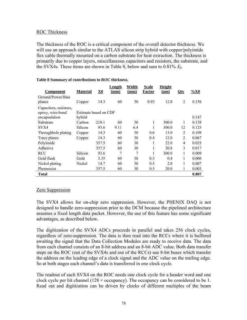
78
ROC Thickness The thickness of the ROC is a critical component of the overall detector thickness. We will use an approach similar to the ATLAS silicon strip hybrid with copper/polyimide flex cable thermally mounted on a carbon substrate for heat extraction. The thickness is primarily due to copper layers, miscellaneous capacitors and resistors, the substrate, and the SVX4s. These items are shown in Table 8, below and sum to 0.81% X0. Table 8 Summary of contributions to ROC thickness.
Component Material X0 Length (mm)
Width (mm)
Scale Factor
Height (um) Qty %X0
Ground/Power/Bias planes Copper 14.3 60 30 0.93 12.0 2 0.156Capacitors, resistors, epoxy, wire-bond encapsulation
Estimate based on CDF hybrid 0.147
Substrate Carbon 218.1 60 30 1 300.0 1 0.138SVX4 Silicon 93.6 9.11 6.4 1 300.0 12 0.125Throughhole plating Copper 14.3 60 30 0.6 13.0 2 0.109Trace planes Copper 14.3 60 30 0.4 12.0 2 0.067Polyimide 357.5 60 30 1 22.0 4 0.025Adhesive 357.5 60 30 1 20.8 3 0.017RCC Silicon 93.6 7 7 1 300.0 1 0.009Gold flash Gold 3.35 60 30 0.5 0.4 1 0.006Nickel plating Nickel 14.7 60 30 0.5 2.0 1 0.007Photoresist 357.5 60 30 0.5 20.0 1 0.003Total 0.807
Zero Suppression The SVX4 allows for on-chip zero suppression. However, the PHENIX DAQ is not designed to handle zero-suppression prior to the DCM because the pipelined architecture assumes a fixed length data packet. However, the use of this feature has some significant advantages, as described below. The digitization of the SVX4 ADCs proceeds in parallel and takes 256 clock cycles, regardless of zero-suppression. The data is then read into the RCCs where it is buffered awaiting the signal that the Data Collection Modules are ready to receive data. The data from each channel consists of an 8-bit address and an 8-bit ADC value. Both data transfer steps on the ROC (out of the SVX4s and out of the RCCs) use 8-bit buses which transfer the address on the leading edge of a clock signal and the ADC value on the trailing edge. So at both stages each channel’s data is transferred in one clock cycle. The readout of each SVX4 on the ROC needs one clock cycle for a header word and one clock cycle per hit channel (128 × occupancy). The occupancy can be considered to be 1. Read out and digitization can be driven by clocks of different multiples of the beam

79
frequency (9.4 MHz) and must be completed within 40 µsec (375 clock cycles). This can be expressed by: 256/M + 12×(1+128×occupancy)/N < 375 clocks, where M is the digitization frequency in units of the beam clock frequency, and N is the readout frequency (defined similarly). If we assume M = N = 1 (e.g., readout and digitization frequencies both equal 9.4 MHz) then the maximum occupancy that would fit in the PHENIX bandwidth requirement is 7%. In fact, the digitization frequency M sets the charge-per channel and will likely be set to a value of ~10 in order to have the signals fill the 8-bit range. It is true that if we use readout frequency equal to four times the beam clock frequency (37.6 MHz, N = 4) we could pass the SVX4 data without zero suppression into the RCC by extending the PHENIX readout time to 41 µsec. However, the readout of the ladder, as shown below, gives a more stringent requirement. To read out an entire ladder, which has as many as 60 SVX4’s, and which similarly must be completed in 40 µsec, we find: 60×(1+128×occupancy)/X < 375 clocks, where X is the RCC readout frequency in units of the beam clock frequency. Here, occupancy with zero-suppression turned off is 0.5 since we do not need to pass up channel addresses in this case. Assuming X = 4 we find that the maximum occupancy is 19%. The consequence is that we need to either a) use on-chip zero-suppression, b) use a significantly higher readout speed (X=10), or c) have more output links per ladder. We have chosen to use the on-board zero suppression feature of the SVX4 because 19% is nearly five times the maximum expected luminosity for the inner barrel in central Au+Au collisions. Therefore zero-suppressed events should always fit in the required length of time (although a mechanism to pass up an error condition will still need to be developed).
Si strip production/testing/assembly schedule The Si strip wafers will be manufactured by a commercial vendor; Hamamatsu of Japan and SINTEF of Norway are currently under consideration (see Figure 44). At the vendor the wafers will undergo resistance and doping tests and then be diced into sensors. Further quality assurance (QA) tests including visual inspection, initial I-V test, and registration in our database, will be performed on all sensors produced upon receipt at RIKEN. Sub-samples of the sensors will be sent to SUNY Stony Brook and UNM for further QA tests including I-V, C-V, and laser pulse tests of each strip. RIKEN will adapt its automated probe station for Si pixel detectors to accommodate testing of strip detectors. SBU and UNM have are negotiated with their respective high energy particle physics groups (D0 and CDF, respectively) the possible use of their testing facilities. UNM facility is being set up as this document is being prepared, while the SBU facility is operational (but presently used for D0 Experiment), and will be handed over to for PHENIX use early in 2005. In order to gain experience, a semi-automatic probe station

80
is being setup at BNL in the RBRC laboratory to be ready in August 2004 and will be used for testing the pre-production sensor tests needed prior to the SBU facility becomes available. Assuming a testing rate of one sensor/day the entire process should take a maximum of four months divided between the three institutions to produce enough good sensors including spares. With the experience of groups responsible for QA testing and assembly of Si trackers at D0, CDF, STAR and PHOBOS serving as guidance, the detailed testing procedure will be developed.
Figure 61 Strip detector production flow chart
As previously stated, enough SVX4 readout chips for Si strip detectors already exist at FNAL. Further processing of SVX4 chips will occur at FNAL, including thinning and metallization, initial QA tests, and dicing prior to purchase by PHENIX. An integrated SVX4/sensor test at ORNL and RIKEN is under way to determine the viability of this particular readout combination (see Table 9). A slightly modified version of the test board developed at ORNL has been prepared and is being used for presently undergoing tests.

81
ORNL has also assumed primary responsibility for development and prototyping the copper/polyimide ROC’s. Each ROC reads out one strip sensor with twelve SVX4 chips and has one rad-hard FPGA (or possibly a custom digital ASIC) called RCC, to serve as local intelligence to direct SVX4 initialization, digitization and readout. Power planes, ground planes and control signals, already present on the ROC’s, are daisy-chained across the ROC’s to form the strip bus. A first test of a fully functional prototype ROC (all components, but no attempt at miniaturization or thinning) is slated to occur by Oct. 2004 (see Table 9).
Table 9 Si strip detector test schedule
Date Test Location Apr. 2004 Si Sensor/SVX4 on the testboard ORNL/RIKEN/BNL Oct. 2004 Full ROC (SVX4/FPGA/strip bus) ORNL Dec. 2004 Si sensor/full 1st round ROC RIKEN Jul. 2005 Si sensor/full 2nd round ROC RIKEN & SBU Jul. 2006 1st full ladder RIKEN
PCB fabrication for the ROC will occur at a commercial vendor from the GERBER file produced by ORNL. Mounting and wire-bonding of the SVX4s and ASICs will also occur at a commercial vendor, using a parts list with x-y locations specified for each component by ORNL. ORNL will be the technical point of contact throughout the entire production, assembly and testing of the Si strip ROC’s. Because a ROC mounted on the Si barrel will be extremely difficult to replace once installed in PHENIX, very strict quality controls are necessary during testing of the production boards. This tight QA procedure will involve an initial system test. Since there are less than 400 ROC’s and all chips will pre-qualified, the duration of these tests will likely be limited by the startup time for the test system, although that system should be largely developed during the testing of pre-production prototype ROC’s. This initial test will be followed by an extended burn-in period and a re-testing. Graduate students and postdocs will participate in this process. With 246 ROC’s in the final system, a requirement for 10% good spares and an anticipated initial failure rate of 10% a total of 300 ROC’s will be manufactured. Qualified ROC’s will be sent to RIKEN and SBU where they will be mated with qualified sensors. RIKEN has recently purchased an automatic wire bonding machine which will be operational in the middle of July 2004, while Stony Brook is in the process of exploring possibilities of procuring one. An initial test of the sensor plus ROC assembly is scheduled for Dec. 2004 at RIKEN.
Each ladder receives its serial programming, clock & control signals and sends its data signals through a pilot module mounted at the end of the ladder to a remote front-end module. This module is relatively simple, basically only serving to drive signals into and out of the active area with as little mass and volume as possible to the downstream processing system. These modules will be fabricated and assembled by a commercial vendor, similar to the ROC’s. Pilot modules will be tested at ORNL with known-good ROC’s and sent to RIKEN and SBU for assembly onto a ladder.

82
Qualified ROC/sensor assemblies and qualified pilot modules will be assembled into ladders and undergo complete system tests at RIKEN and SBU. A first full ladder test should be ready by the middle of 2006. Table 1 summarizes the test schedule for Si strip detectors.
The QA procedures and criteria for acceptance and failure of the strip sensors and the ladders will be developed drawing on the significant amount of experience already in place at UNM and Stony Brook (in the high energy physics groups) involved in CDF and D0/ATLAS, respectively. RIKEN plans to train some of their young student scientists under the guidance of the Stony Brook D0 group preparing for their L0 Si detector upgrade during the middle and latter half of the 2004. The details of QA criteria for the strips and ladders will be developed in due course in consultation with the vendors, the understanding of each of the components as prototypes are made, and in consultation with the experienced groups in high energy physics in this field. The QA criteria for the strips and the ladders will be separated in to two categories: The criteria for dimensional or mechanical properties and electrical properties. The QA for mechanical properties will include physical dimensions of sensors and ladders, thicknesses and the widths along the length of the strips and ladders, edge chipping due to cuts and related tolerances, alignment at various joints including metallization with implant. These other such criteria can be tested using a detailed visual inspection or/and optical metrology. The QA for the electrical properties will include measurements of following properties to be within a certain tolerance limits. They include for example, the CV and IV curves, the leakage current on strips (Istrip), the inter-strip resistance (Rint), and the inter-strip capacitance (Cint) at a specific frequency. Both types of tests, mechanical and electrical, will be further separated in to three types:
1. Key tests: These will be performed on every sensor and every ladder assembly. These are most important because they determine the minimum performance of the strips and ladders as individual entities.
2. Subset test: These will be performed on a defined fraction of strip sensors and ladders, which pass the key tests. The main goal of subset tests is to verify compliance with specification in depth. Typically, the fraction of sensors and ladders that will undergo these tests will be higher during the early stages (or prototypes) and in the production stage depend on the overall experience of the quality of production and some key correlations to be developed at a later stage with the vendor QA data. The subset tests will be done with the automated probe stations under computer control.
3. Diagnostics tests: These will be done on a fraction of strips and ladders on a fraction of units passing the Key tests, and also on the units flagged
The frequency of subset tests and diagnostic tests will be determined as we proceed through the prototyping process.

83
Two other issues not mentioned up to now but assumed is that all testing will be done in a controlled environment, i.e. in clean rooms meeting criteria specified by the vendor. All personnel handling the sensors and ladders shall undergo training & practice in all phases of manipulation involved in the process. There will also be a clean & dry storage facility for ladders not being tested or used. The clean rooms will control the temperature and humidity. The second issue is keeping a good record of the environmental conditions for each tested sensor and ladder in a complete database. The database will include will include not only the results of the QA associated with a particular sensor/ladder but in addition the temperature and humidity, date, testing center, and any other comments that the testing crew deems important at the time of the test. RIKEN constructed the laser test setup similar to that in the BNL Instrumentation for this purpose and an identical setup will be moved / set up at BNL Chemistry for final QA tests before the completed ladders are assembled onto the barrel frame.
4.4 Mechanical Structure and Cooling A conceptual design of the silicon vertex detector was commissioned by the LANL group to HYTEC, Inc. HYTEC is the mechanical designers for the ATLAS silicon group and has 15 years of design experience with silicon vertex detectors. For PHENIX they have also designed the station-1 muon detectors and the station-2 spider and also did the finite element analysis of the station-3 octants. The VTX mechanical conceptual design was finished and the report is summarized in this section. [http://p25ext.lanl.gov/~hubert/phenix/silicon/HTN-111003-0001.pdf]. The next steps following this conceptual design are to fully specify the requirements for the VTX mechanical support and cooling. These requirements will incorporate the integration needed for all the upgrade PHENIX detectors in the inner region, including the VTX barrel described in this proposal, the end-cap described in Appendix A, and the HBD/TPC to proposed later. Hence there are two major mechanical engineering tasks contained in this proposal: 1) the internal support and cooling of the VTX detector (described in this section) and 2) the integration of the VTX detector into the inner region of PHENIX (described in the next section). For the internal support and cooling of the VTX detector, the major results of the conceptual design are:
• The use of sandwich composites will satisfy the radiation length requirements and provide the required stiffness.
• The outer frame structure should be a single diameter encompassing both the barrel and end-caps.
• The modular clamshell design can satisfy the stability requirements provided the connection issues are studied further.
• An octagon arrangement is suggested to facilitate utility routing and fabrication. • Structural end disks at either end of the structure are recommended to prevent
deformation

84
• The ladders should have a simple support at one end and floating support at the other end to minimize thermal strains
The R&D issues identified are:
• Building prototypes of ladder assemblies to verify calculations. • Building full-scale prototype to test static and dynamic stiffness. • Develop connections of modules. • Develop support design. • Refine calculations and develop full concept for 0 deg operation if necessary.
Design Criteria The goal of the study is to establish a feasible design and to identify outstanding design issues. The study is based on a preliminary list of design requirements and a straw-man layout of the detector structure. To adequately address all structural and mounting issues a fully integrated design, which includes the barrel detectors and future end-caps extension, is needed. This design needs to address all integration issues not only for the barrel and the end-cap vertex trackers, but also with other potential PHENIX upgrades. The design requirements of the conceptual study were,
• Modular Design o End-caps detectors can be mounted independently at a later time o Support structure separated vertically into two half shells
• Detector Coverage o Hermetic design o Four barrel layers o Four end-cap layers in each forward section o Fiducial volume < 20 cm radius, z < 40cm
• Radiation length goal < 1% per layer • Room temperature operation desirable, 0 deg Celsius if needed • Dimensional stability < 25 microns
In the conceptual study, the ALICE1LHCb pixel hybrids for the inner layer and silicon strip detectors with SVX4 readout for the three outer layers provide the basis for cooling and radiation length analysis of the barrel detector. At the time, for the end-caps a modified ALICE type chip that has 1/5 to 1/10 of the number of pixels was assumed2. These choices resulted in a estimated heat load of typically 0.7 W/cm2 for the barrel and 0.1 W/cm2 for the end-caps.
2 After the completion of this study a more promising technology for the end-caps has been identified (see appendix A), but the heat load is expected to be similar.

85
Structural Support
The selection of materials for the support structure is based upon the above criteria where the most important material properties are high radiation length, low density, high stiffness, and availability. Out of three candidates (i) beryllium, (ii) graphite fiber reinforced plastic (GFRP), and (iii) Carbon-Carbon, the GFRP was chosen for the study because of its wide availability, works well in sandwich composites, and has good radiation length and strength properties.
Structural Analysis The structural analysis includes two studies, a first study using finite element analysis models and the resulting modal frequencies to look at dynamic stiffness of tracker concepts and a second study to look at the static stiffness with mass loaded structures. The lower modal frequency limit is set at 70 Hz on a fully loaded structure so that the natural frequencies due to environmental conditions such as pumps, traffic, etc. do not couple into the structure and cause instabilities greater than 25 microns.
Figure 62 Design concepts studied for the vertex detector support structures. The center most concept with the constant outer diameter shell had the highest fundamental frequency.
Figure 63 First mode shape that dominated the dynamic structural stiffness analysis

86
Various support structures shown in Figure 62 were studied. The center most structure has the highest frequency limit. The dumbbell shaped structure has the lowest mode frequencies below 53 Hz while the concept with the uniform shell with constant outside diameter has the lowest fundamental mode at 132 Hz, well above 70 Hz. In Figure 63 the associated first mode shape of the concept that has the highest fundamental frequency is shown The static analysis under gravitational load is shown in Figure 64 for the concept with the uniform shell. A 1.0 G load is applied vertically to the fully loaded structure. The maximum displacement is 14.5 microns and the maximum stress is 130 psi. These satisfy the design criteria so the uniform shell with constant diameter has been chosen as the concept to be pursued.
Figure 64 Displacement and principle stress from a 1.0g gravity load on a full mass loaded structure
Detector Ladders and Cooling The mechanical design draws on a ladder concept for supporting both the inner layer of pixel and the outer strip detector layers. The pixel detectors and strip detector array are arranged in a longitudinal fashion, and at a slight cant angle, which provides a small amount of overlap for hermeticity. The pixel and silicon strip detector both contain on-board electronics, thus necessitating cooling along the Z-axis of the detectors, thus the ladders simultaneously must provide mechanical support and cooling. The barrel region is about 30cm in length and thus the ladders need supported only at their ends. Open ring like structures at the two ends of the ladders, Figure 65, provide attachment points for the ladders and serve to combine the staves into two halves of a clamshell. Figure 65 also illustrates the cross section of a ladder structure, it is composed of a thermal plane (Carbon-Carbon) onto which the pixel modules or strip detectors are mounted. The thermal plane collects the distributed electronic heat, as well as providing a conductive path to the cooling tube. All elements are bonded with thermally conductive, rigid setting adhesives. The omega shaped piece holding the cooling tube on to the C-C thermal plane provides significant stiffness to the ladder.

87
Figure 65 3D model of the barrel region on the left and the ladder structure on the right showing a cooling tube mounted on a C-C thermal plane and the sensor and electronics on the underside.
Cooling Analysis The total heat load that must be removed from the vertex detector is approximately 2.2 kW, which is dominated by power dissipation in the barrel detectors. There are generally two choices for the coolant system, single-phase and two-phase. In a single-phase system the coolant is circulated through pipes in a closed system. In a two-phase system the coolant arrives as a liquid and then evaporates into the detector volume where it is collected and removed. The two-phase system has the advantage that it is a more efficient coolant and a lower total mass is required. However, the two-phase system is more difficult to implement because of issues concerning more sophisticated temperature and pressure control. The single-phase system is simpler in implementation and design and therefore chosen to be the baseline design. An important issue in the design of the mechanical structure is the operating temperature. In the initial design requirements we stressed the importance of room temperature operation and the design presented here is based on this assumption. However, the design engineers have developed the concepts that will allow operation at 0 deg by using suitable coolants that can operate at these lower temperatures. A more detailed study of the enclosure and thermal stresses would need to be done to confirm the concepts at reduced operating temperature. After this study was concluded, it was noted that the outer 3 layers of the barrel might perform better at 0 deg because of the mismatch between the SVX4 chip which is an AC coupled device and the strip sensor which is a DC coupled device. The concern centered on leakage currents from the sensor that could saturate the SVX4 chip. The other option is to reset the chip regularly during the empty beam-crossing at RHIC. The selection of coolants was based on previous experience in the design of the ATLAS detector and the choice was to use one of several perfluocarbon candidates, commonly called fluorinerts. These fluids can be used in either a single or a two-phase system and

88
are environmentally acceptable. Based on a number of considerations the fluorinert C5F12 was chosen as the baseline. In comparison to the ATLAS detector the heat load is very modest and a single-phase system can be used. Since the barrel is only 30 cm long the design assumes that the ladders need only be supported at the ends and the cooling structure can serve as the means of joining the two half ladders of the pixel layers. The concerns with this approach center on,
• Out of plane distortions from thermal strains due to different CTE’s • Gravity sag • Mass of the structure exceeding radiation length guidelines
A series of calculations were done on the thermal aspects of this concept by using the outer barrel ladders since the greatest total heat load, 27 W, exists there. Using a temperature rise of 2 deg C as the maximum allowed temperature rise in the ladder the results indicate a good solution exists with an Al tube diameter of 3mm and a wall thickness of 0.2 mm. The result for the out-of-plane distortions for room temperature operation is quite acceptable, 0.18 microns. For the possible design requirement of 0 deg operation the out-of-plane distortions increase because of the difference in CTE’s of the C-C and silicon but is still acceptable at 3.5 micron. Bowing along the length of the ladder due to thermal strain because of the temperature gradient at room temperature is an acceptable 6.8 microns. However, if the detector is cooled, the bowing increases to over 80 microns. This is more than desirable so addition R&D is necessary.
Figure 66 Left panel shows the out of plane distortions and the right panel shows the bowing for the 0 deg solution.
Figure 66 illustrates the 0 deg solution. While the temperature drop for the coolant is still the same as at room temperature the reference temperature is always 25 deg since that is

89
the temperature of assembly. The increased bowing is due to reducing the operating temperature to 0 deg. For the gravity sag the general bowing of the ladder is acceptable at 18-20 microns.
Radiation Length The radiation length budget for the ladder describe above exclusive of the sensor and electronics consists of:
• Composite thermal backplane • The cooling tube and tube support • The omega piece • The coolant
The combined radiation length is 0.7% with the single largest contributor being the tube support (0.28%). The liquid coolant contributes 0.074%, cooling tube ~0.1%, and the omega piece and C-C facings ~ 0.2%.
4.5 Detector integration into PHENIX Once the individual detector components and the mechanical support structures become available, the VTX system needs to be assembled, integrated into the PHENIX setup, and connected to the support and ancillary systems as well as to the DAQ. These steps are critical for the successful completion of the project and need to be addressed well in advance and in close contact with the developments of the detectors and support structures.
VTX detector assembly Each step from delivery of sensors and readout chips, to the assembly of detector ladders, to their final mounting in the mechanical support structure, will require intensive quality control and testing of the components. Special equipment, infrastructure and expertise are necessary to complete these tasks. We have started to plan the necessary steps and to optimize the use of expertise within our collaboration and the institutions that we cooperate with.
Error Budget Our general philosophy will be to utilize fixtures wherever possible to allow the assembly of the VTX to be within the tolerances established by simulations. This will be

90
accomplished by adhering to a strict error budget. The errors can be separated into intrinsic errors due to the strip width and assembly errors. The intrinsic error due to strip width is simply width/√12 = 23µm for an 80 µm micron strip. The assembly errors are due to the following,
a. locating the sensors to the precision alignment pin holes on the ladders b. placing the ladders onto the structural frame c. placing the assembly into the hermetic enclosure.
By using precision fixtures we will minimize these assembly errors to < 10 µm each. A precision drill fixture can be used to drill the pin hole on the ladders and in the structural frame. The structural frame will be held rigidly in a fixture that will allow positional changes during ladder installation.
Ladder Assembly - pixels The goal of the assembly procedure of the ladders is to insure that the sensors are accurately located on the cooling supports with respect to the alignment pins. This will allow manual placement of the ladders on the structural assembly. The bump bonding will be done at an industrial facility, VTT. All necessary steps in testing of the bump bonded sensors will be carried out at CERN or at facilities of the RIKEN institute. For the silicon pixel detectors the major steps that need to be taken are,
• Test sensor assemblies which include one sensor and 4 readout chip. This test will require a full mini-DAQ and cooling system at each testing facility. Since the readout buss will not be attached yet, a probe station will be used. A fixture will be required that will allow the chips to be cooled without being glued. • Attach readout bus to pilot card and test. • Attach readout bus and pilot card to sensor assemblies and test. • Assemble half ladders, combining readout bus, two sensor assemblies and pilot
module and test. This is the most critical mechanical operation in assembling the VTX. The sensors must be attached to the ladder with an accuracy of <10 µm.
This can be done by either a very sophisticated fixture such as the one designed by the ALICE group or by an accurate pick and place machine. The alignment pins will be the fiducials.
Ladder Assembly – strips .
For the testing of the strip sensors and the SVX4 chips, we will benefit from the knowledge of the BNL Instrumentation Division and the cooperation with the FNAL silicon laboratory. The ORNL group, which is developing the ROC, will work together with other groups, including University of New Mexico, to test and assemble the ROC’s.

91
The University of New Mexico group draws on knowledge and experience gained during similar work for the ATLAS and CDF vertex detectors For the silicon strip detectors the major steps that need to be taken are:
• Fully test sensor at the BNL laser test stand. • Fully test the SVX4 chips at the FNAL electronics test facility • Test bare readout card • Mount SVX4s on ROC’s • Test ROC assembly. This will require cooling fixtures for the chips and mini-
DAQ’s at all fabricating institutions • Attach ROC’s to sensor • Send to wire bonding facility • Test ROC/sensor combo • Assemble ROC/sensors into ladders. This will be done in manner similar to that
done for the pixel detectors. • Attach pilot modules to ladder • Test complete ladder, needs complete cooling system and mini-DAQ.
Half detector assembly All fully tested ladder assemblies, pixel and strip will be received by the BNL/Stony Brook and retested to insure that nothing was damaged in transport. The ladders will be inserted into the structural assembly beginning with the innermost layer proceeding to the outermost layer. The structural assembly will be securely held in an accurate holding fixture that will allow the structural assembly to be rotated so the ladders can be placed on the pins and fastened into place by either screws or glue and an accurate survey can be conducted and recorded. A final test of the completed half detector will be done under a full system test, full cooling and readout. If ladders are shipped to the assembly in small lots then much of the VTX assembly can be done in parallel to the ladder production.
Integration into PHENIX
Mechanical mounting The mechanical mounting of the detector will be done by BNL PHENIX Operations, in close collaboration with HYTEC. The current concept would be similar to the existing PHENIX MVD mounting. This will support the VTX detector directly on the copper nose cones with attachments to the ends of the detector. The two halves of the split barrel will be either hinged together at the top or the bottom, or be mounted independently. The development of this concept will require careful consideration of a number of issues, including precision and stability requirements, accommodation of future detectors (e.g. silicon vertex detector end-caps to cover the muon detector acceptance, and a micro Time Projection Chamber (TPC) in the acceptance of the central arms), the attachment and routing of cables, fibers and hoses. Figure 67 shows how the vertex tracker is placed with other proposed upgrade detector in PHENIX in a small space inside of the PHENIX central magnet.

92
Figure 67 The inner region of PHENIX central magnet with the envelopes of proposed upgrade detectors. The silicon vertex tracker (SVXT), a micro TPC, and nose cone calorimeters are shown.
Support and Ancillary Systems Additional platforms installed on top of the PHENIX central magnet yoke will be required to support electronics racks and cooling system equipment. These racks will include space for low voltage and bias supplies, and whatever readout electronics for the silicon detectors. The platforms must also provide area for cooling system pumps, and compressors or chillers. In addition, these platforms will be used for ancillary systems in future detector upgrades in the central magnet such as the HBD.
Beam pipe A new beryllium beam pipe with a smaller 4 cm inner diameter and 500 µm nominal thickness will be critical to perform the anticipated measurements. The inner surface of this pipe may need to be NEG (non-evaporative getter) coated to help reduce beam induced vacuum instabilities. This technology is currently being implemented in the upcoming RHIC run. The new beam pipe will need to taper out to match the standard 5 in diameter lines of the RHIC rings.

93
DAQ The VTX readout system will be matched to the requirements of the PHENIX high rate data acquisition (DAQ) system. The current DAQ system has a bandwidth corresponding to approximately 12.5 kHz level 1 (L1) trigger rate with a planned upgrade to 25 kHZ. Currently each front-end module (FEM) sends uncompressed events of fixed length to Data Collection Modules (DCMs) through a gigabit optical link. Each DCM has four sets of optical receivers, FPGAs and digital signal processors (DSP), which zero-suppress and buffer the events from four FEM’s. An additional DSP is used to merge the data from the four sets. The DCMs and FEM’s pipeline events with the capability to buffer at least 4 or 5 L1 triggers. Since the FEM data is of known length no data flow control between FEM’s and DCMs is necessary in this design and only the DCM participates in the busy logic. Because the VTX will deliver substantially larger data volumes than the currently operated detectors and it will be necessary to zero suppress the data at the front-end before it is transmitted to DCM's. As a consequence some of the current DCM-functionality must be taken over by the pilot modules on the detector and the FEM’s off the detector. In particular, after the zero suppression, the FEM data will no longer be of fixed length and therefore the FEM’s must participate in the busy logic. Since the new requirements are common to most of the planned PHENIX upgrades detectors we have launched an R&D effort to develop the new DCM's independent of this proposal. We anticipate that the development will be completed within 2 years, in time to produce new DCM's for the VTX detector. Once the new DCM's are completed the PHENIX Electronics Facilities and Infrastructure (EF&I) and Online Computing Systems (ONCS) groups will guide the electronic integration and readout of the VTX.

94
5. R&D With the help of institutional contributions it was possible to maintain a small, but well focused, effort over the past two years to explore technologies for silicon detectors suitable for PHENIX. The results of these investigations are the basis of the present proposal. The outcome and corresponding technology choices, which are the ALICE silicon pixel hybrid detectors and a BNL silicon strip sensor with SVX4 readout, have been discussed in section 4. More recently the R&D effort has shifted towards adapting the technologies to the PHENIX requirements and developing prototypes of detector elements, readout electronics as well as mechanical support. This effort, which will continue through FY05, is supported by generic R&D funds provided to PHENIX through BNL and institutional contributions. All R&D issues have already been addressed in chapter 4. Here we summarize the main issues. The readout speed of the ALICE1 pixel chip is limited to 10 MHz, which means that it takes 25.6 µs to read one chip. A sequential readout of all chips on a ladder, like it is done in ALICE, is out of question since it does not meet the PHENIX design specification to read each detector in 40 µs. Several options to overcome this limitation are under study. They all involve parallel readout on the ladders, which require developing a new readout bus and a new pilot module. For the pilot module we have focused on modifying the ALICE pilot, a custom ASIC developed at CERN. The modifications of the ASIC are implemented at CERN together with the designers of the original pilot chip. A first design is in production and will be tested in Fall 2004. Options for the necessary modifications of the readout bus are currently being discussed with vendors in Japan. Another R&D issue concerns the readout of the BNL silicon strip sensors. First prototype sensors have been tested in the laboratory and in beam. The performance is very encouraging, however, some limitations have been found which we believe result from poor signal-to-noise ratio of the readout electronics used. The second generation of sensor prototypes are now available, and they are being tested. These tests include comparing AC and DC readout of the sensors as well as reading the sensors with SVX4 readout chips. In the present setup the sensors are readout with SVX4 readout modules obtained from CDF at FNAL. Based on the experience gained in these tests a first prototype of the PHENIX read out card (ROC) will be developed. The sensor design has recently been optimized. The new design minimizes the dead areas present in the first prototypes, in addition the bond pads have been relocated and adapted to the dimensions of the SVX4 chip in order to simplify the ROC design. New prototypes are currently under development by two vendors.

95
For both pixel and strip detectors data from the front-end electronics, i.e. pixel pilots and strip ROC’s, must be readout into the PHENIX DAQ system. This task is carried out by front end modules (FEM) which collect data from the front end and transfer it to PHENIX data collection modules (DCM). The design of the FEM’s is being studies and prototypes will be developed during 2005. In addition the design of the mechanical support structure needs to be investigated. This includes a full specification of the requirements, prototyping staves that carry pixel and strip detector ladders, support structures for these staves, as well as a design studies for a cooling system. We need to pursue and complete these topics over the next year to start EDIA and construction of the VTX in FY06. In summary the R&D of the projects and the milestones are: Inner Pixel layers
• Pixel Bus, multiple layers, fine lines on Kapton o Uses ALICE bus as starting point, draws on rapid advances in signal
interconnect technology o First design and prototyping completed December 2004 o RIKEN manpower
• Pilot Module o Uses ALICE pilot card as starting point, develop new digital PILOT, use
existing ALICE analog PILOT and optical chips o RIKEN manpower
• Pixel FEM o Develop pixel FEM based on PHENIX drift chamber FEM. o First prototype complete by July 2005 o SBU manpower
Outer Strip Layers
• Readout card for SVX4 o Design and develop prototype based on FNAL experience o Prototype cycle completed by September 2005 o ORNL manpower
• Serpentine strip sensor o Based on tests of first prototypes o Final tests of prototypes with SVX4 by December 2004 o BNL, SBU, RIKEN manpower
• Pilot/FEM module o First prototype cycle completed by August 2005 o ORNL, ISU manpower

96
Auxiliary System and Integration
• Specifications of system requirements o Specify heat load and mechanical tolerances November 2004 o BNL/LANL/HYTEC manpower
• Design study of mechanical support o Outer structure, ladder staves and support o Design study based on system requirements completed September 2005 o LANL/HYTEC manpower
• Design study of cooling system o First design based on system requirements, completed November 2005 o LANL/HYTEC manpower

- 97 -
6. Project management and responsibilities The organization and management of the proposed effort is embedded in the management structure of the PHENIX experiment, which is part of the BNL RHIC project. The new organization must satisfy a number of requirements including a clear interface to the existing RHIC and PHENIX management structure, clear roles and responsibilities within the existing PHENIX subsystem structure. Particular attention has to be paid to the fact that a significant portion of the project is supported by foreign contributions. Clear deliverables, responsibilities for deliverables and the accountabilities of the participating funding Agencies have to be defined. These responsibilities will be formalized in memoranda of understanding (MOU's) between PHENIX and the participating institutions. In this section, we outline our proposed management organization and delineate responsibilities within the project.
6.1 Project background The proposed project is part of a detailed upgrades program to enhance the physics capabilities of PHENIX over the next 8 years. Realizing this plan will enable PHENIX to remain competitive well beyond the turn on of LHC expected for 2008, as well as to advance our understanding of QCD by fully exploiting the unique spin physics capabilities of RHIC. The plan covers a broad range of measurements in A+A, p+A, and p+p and its goal is to provide key measurements which currently can either not be addressed at RHIC or only with limited accuracy. The development of the PHENIX upgrade program started in response to the NSAC long-range plan developed in 2000. The strategy was consolidated at a workshop in Montauk, NY March 2001 and at BNL August 2002. Since then individual upgrades have been followed up in detail within four PHENIX study groups. The PHENIX upgrades plan was first presented to BNL management in a proposal seeking funds to initiate a broad-based R&D effort to develop the detector technology necessary to realize our goals. BNL charged a Detector Advisory Committee (DAC) to review the R&D plan. After the first review December 19-20, 2002, at BNL the committee named the PHENIX silicon vertex tracker a high priority in the future development of PHENIX. Some quotes from this report: "Physics Motivation: … Charm has emerged as valuable probe of QCD dynamics … The measurement of hadrons with open charm requires excellent vertex identification, which can only be achieved with state of the art silicon vertex detectors …" "PHENIX Microvertex Tracking Detector: The extension of the capabilities of the PHENIX detector to provide a direct measurement of charm and open beauty will have

- 98 -
major impact on a number of physics questions both in A+A and p+p collisions. This upgrade is therefore a very high priority in the future development of PHENIX.“ “It is likely that a detector system with adequate performance can be constructed using existing technology and it is therefore possible and desirable that a detailed proposal for this upgrade be in place in time for inclusion in the planning process for FY05 construction funds." Responding to the DAC review, the silicon study group developed a PHENIX internal letter of intend proposing a two component silicon vertex tracker system, one component - a barrel detector - extending the capabilities of the PHENX central arm detectors and the other - an end-cap detectors - extending the physics reach of the muon detector system. This LOI was reviewed in March 2003 at a joint meeting of the PHENIX detector council (DC) and executive council (DC). Following their recommendations PHENIX management (PM) endorsed both projects and charged the silicon study group to develop a proposal for a silicon barrel detector for immediate presentation to DOE through BNL. The DAC met again on Nov 22-23 2003 and reviewed a preliminary version of the VTX proposal. The committee report stated that “the Collaboration has made impressive progress…. and a viable design is close.” They raised seven issues or concerns, which have been addressed in the proposal in detail. The issues and concerns as well as our response are summarized in the following: 1) Concern on the hit occupancy in the 2nd layer: We now use Si pixels in both the first and second layer of the detector. The occupancy of the 2nd layer has now improved from >10% to only 0.16%. The number of strip layers are reduced to two from three, and we changed the radius of these two outer layers to 10 cm and 14 cm. In this new configuration, the highest occupancy is at the 3rd layer and it is now only 4.5% in central Au-Au collisions. With the new detector geometry we have also demonstrated the track-vertex matching capabilities by a realistic simulation. 2) Explore if the number of silicon detector technologies can be reduced: We have decided to use ALICE pixel technology for the two inner layers and the BNL silicon strip sensor combined with the SVX4 read-out chip for the outer two layers. This choice is driven by the goal to complete the barrel VTX detector for the next full energy Au+Au run which is anticipated for RUN8. The possible reduction of the number of technologies would imply to use the PHX pixel development. This PHX technology is considered for the end-cap extension of the VTX detector, where neither the ALICE pixel nor the BNL sensors can be utilized. However, the R&D for this technology is still at an early stage, and will require approximately 2 years to advance to the level of the currently proposed technologies. Choosing the PHX technology for the VTX barrel would have delayed the project by about 2 years. 3) Necessity of a full system test of SVX4 and strip sensor to evaluate signal/noise:

- 99 -
This test is underway. We have a new, version-2, prototype sensor in hand and a test of the version-2 sensor with the SVX4 hybrid is under-way. The initial result is quite encouraging. The recent development of the test is included in the updated chapter 4.3. 4) Utilize the silicon detector expertise at BNL: BNL Instrumentation, specifically Zheng Li, is part of the VTX collaboration and key to the development of the silicon strip detectors. 5) Define more clearly the organization structure and responsibilities, We now have identified personnel for essentially all leading positions of the VTX project. This is reflected in the management organization chart (Figure 67 in the proposal). We also included a new table (Table 10) which summarizes the professional background of the lead managers in the VTX project. Subsystem Manager: Yasuyuki Akiba Deputy subsystem Manager: Craig Ogilvie Inner Layer (Pixel) Manager: Hiroaki Ohnishi Outer Layer (Strip) Manager: Abhay Deshpande Auxiliary System and Integration Manager: Rober Pak. Software Manager: A. Lebedev In addition, we plan to support a full time project system engineer to over see integration of the VTX detector. The costs are now included in the VTX budget. We have also identified leadership for most sub-tasks specified in the management chart. The technical expertises and experiences of the collaboration are now summarized in tables (Table 11 to Table 15). 6) Include details on system tests during prototyping and on the final assembly and QA of the sensors, electronics and ladders in the schedule: We added a new subsection on the system tests, the Q/A procedure, and the final assembly in both of the pixel detector (chapter 4.2) and the strip detector (section 4.3). 7) Document the schedule for performing a “ladder” test, which includes sensor, electronics, bus, readout and mechanical ladder. A “Pixel system test” and a “Strip system test” are now explicitly included in the schedule of the project. (See Figure 70 and Figure 71)
6.2 The management plan for the VTX
PHENIX management structure The VXT project is part of the PHENIX project and as such integrated into the PHENIX management structure as described by the PHENIX bylaws. The PHENIX Detector Council (DC) will advise PHENIX management on the design, construction, and integration of the VXT. The DC is co-chaired by the operations manager (E.O'Brien) and

- 100 -
the upgrades manager (A. Drees). The VTX subsystem manager will serve as a member of the DC.
PHENIX subsystem leadership We expect that the proposed VTX project will be funded through two agencies, the DOE Office of Nuclear Physics (DOE-NP) and the RIKEN Institute. A successful completion of the VTX will require close collaboration and well-defined responsibilities and scope of the contributions of both agencies in terms of deliverables. The deliverables and foreign contributions are outlined below. Within PHENIX, the responsibility for the VTX subsystem will be shared by the subsystem leader, Yasuyuki Akiba (RIKEN) and his deputy, Craig Ogilvie (ISU). The subsystem leader reports to PHENIX PM and will represent the VTX in the PHENIX DC. Simultaneously, Ogilvie will serve as the DOE contract project manager (CPM), and will have the fiscal and construction responsibility for the DOE funded deliverables as outlined in this proposal. This involves appropriate planning, budgeting, and reporting. Akiba will serve as RIKEN counterpart and have similar responsibilities for the RIKEN funded deliverables.
Figure 68 Management chart of the VTX project. The fiscal responsibilities for the individual tasks are specified in bold letters. The institutions participating in each task are given in italic. In PHENIX the DAQ is a separate subsystem and therefore not connected to the VTX management.

- 101 -
Role of BNL Because we expect that all DOE funding for this effort will be directed through the BNL Physics Department, BNL line management will have ultimate fiscal and management responsibility for the construction of the VTX and for its subsequent operation. Included in the management chart is the position of Lead Electronic System Engineer. This person has responsibility to oversee the electronics integration of both strips and pixels and will be funded with construction dollars. The ideal candidate is one with extensive experience with Si detector projects. More details on the management personnel can be found in Table 10.
Table 10 Professional Background of the lead managers in the VTX project.
People VTX FTE now
VTX FTE after 2006
Experience
Subsystem Leader Yasuyuki Akiba (RIKEN)
50% 100% Managed construction and installation of RICH for PHENIX, approximate budget $10M. Physics Working Group convener for PHENIX. A deputy spokesperson of PHENIX.
Deputy Subsystem Leader Craig Ogilvie (ISU)
50% 100% Led PHENIX Silicon study group. Managed construction, installation of multiplicity counter for E866 AGS. Physics Working Group convener for STAR and PHENIX
Project System EngineerTBD
100% Full-time systems engineer with Si detector experience to oversee integration of strips and pixels
Inner Layer Manager Hiroaki Ohnishi
50% 100% Leading RIKEN group at CERN testing and assembling pixel detector for NA60 and ALICE
Outer Layer Manager Abhay Deshpande
50% 100% Several years experience in PHENIX, managed design and installation of the New Trigger Counter.
Auxillary Systems and Integration Manager Robert Pak
50% 100% Several years in PHOBOS as RHIC Liaison. Responsible for day-to-day operations in PHOBOS.
Management
Software A. Lebedev
50% 100% Oversee simulations, reconstruction, DCA, efficiency calculations.

- 102 -
Specification of deliverables Figure 68 shows the construction and organization chart for the VTX project. The VTX is divided into subprojects, which themselves are divided into tasks. The tasks closely relate to deliverables, which need to be completed before the VTX construction project can be considered complete. The proposed fiscal responsibility for each deliverable, either RIKEN or DOE, is indicated in brackets. Expected institutional involvement is listed together with the fiscal responsibilities in Figure 68. The present and future involvement of individual institutions is discussed in more detail in the next section. Outer layer silicon strip detectors:
• Silicon strip sensors designed and tested to specifications (RIKEN) • SVX4 readout cards (ROC's) developed and manufactured (DOE) • Strip sensors integrated with ROC's (DOE) • Pilot modules to readout ROC's from detector assembly (DOE) • Front-end modules (FEM's) to collect data from pilot modules (DOE) • Detector ladder, sensors-ROC's assemblies with pilot module mounted on readout
bus (DOE) • Commissioning of strip detector ladders (DOE)
Inner layer silicon pixel detectors: • Tested sensor assemblies which include one sensor and 4 readout chips (RIKEN) • Readout bus to read data from sensor assemblies manufactured and tested
(RIKEN) • Two sensor ladders mounted on readout bus and tested (RIKEN) • Pilot card to readout pixel hybrids from one readout bus produced (RIKEN) • Half ladders, combining readout bus, two sensor ladders and pilot module
assembled and tested (RIKEN) • Assembly and commissioning of half ladders to full ladders (RIKEN) • Front-end modules (FEM's) ready to collect data from pilot modules (RIKEN)
DAQ system • Data collection modules for pixel and strip detector manufactured and tested
(DOE) Auxiliary Systems and Integration
• System support requirements specified, including heat loads, power distribution, mechanical tolerances and ground scheme (DOE)
• Mechanical support structure designed and manufactured (DOE) • Ancillary systems operational, including power distribution and cooling system
(DOE) • Strip and pixel detectors ladders mounted in mechanical support (DOE) • Full system tested in assembly laboratory (DOE) • Commissioning of full detector system (DOE) • VTX installed at final location in PHENIX experimental (DOE) • Full system test in PHENIX (DOE) • Integration into PHENIX DAQ system (DOE)

- 103 -
6.3 Manpower for Tasks The following tables document which tasks people will work on in the VTX project. Table 11 Collaboration members working on the inner-layer/pixel sub-task.
People Experience/Experetise Inner Layer Manager
Hiroaki Ohnishi (RIKEN) Leading RIKEN group at CERN testing and assembling pixel detector for NA60 and ALICE
Pixel Readout chips, bump-bonding, hybrids
Johann Heuser (RIKEN) 1992-1999: Development of pixel detectors, RD19 Collaboration, CERN. 1994-1999: Construction, Commissioning, Operation of the DELPHI pixel detector and DELPHI Silicon Tracker. Since 2001: Construction, Commissioning and Operation of the NA60 pixel detector.
Hiroyuki Kano(RIKEN) ASIC development. Modify PILOT chip at CERN. Pixel Pilot module Jonathon Crandall (ISU) Masters student in EE Pixel Bus Atsushi Taketani (RIKEN) Construction, commissioning, and operation of PHENIX
muID. Table 12 Collaboration members working on the outer/strip sub-task.
People Experience/ Expertise
Outer Layer Manager
Abhay Deshpande (SBU) Several years experience in PHENIX, managed design and installation of New Trigger Counter.
Junji Tojo (RIKEN) Led PHENIX strip R&D last two years.
Yuji Goto (RIKEN) Convener of PHENIX Si study group 2000-2003 Junkichi Asai (RBRC) Si detector Q/A K. Boyle (USB) Grad student. Si detector Q/A Zheng Li, Don Elliott, Rolf Beuttenmuller (BNL ID)
Designed and fabricated several similar sensors
Naohito Saito (Kyoto)
Silicon strip sensors
Manabu Togawa (Kyoto) Graduate student in physics Vince Cianciolo (ORNL) Managed design and installation of FEE for PHENIX MuIDPaul Stankus Miljko Bobrek (ORNL) Several years experience designing analog, digital systems,
including PHENIX front-end electronics systems. Kim Castleberry (ORNL) As above Chuck Britton (ORNL) As above Bill Bryan (ORNL) As above
Silicon strip read-out
Alan Wintenberg (ORNL) As above Miljko Bobrek (ORNL) Designing analog, digital systems, including PHENIX FEE.Craig Ogilvie (ISU) Gary Sleege (ISU) Designing digital systems John Lajoie (ISU) Designing/implementing PHENIX LVL1 systems
Silicon strip pilot
Steve Skutnik (ISU) Masters student in Physics Doug Fields (UNM) M. Malik (UNM) SVTX detector Q/A Rachid Nouicer (BNL Chem)
Construction, installation, and commissioning of PHOBOS
Hubert van Hecke (LANL) From MVD: QA, assembly, testing, readout electronics for silicon strip and pad detector assembly
Silicon strip assembly testing
Jan Boissevain (LANL) As above

- 104 -
Table 13 Collaboration members working on the auxiliary systems/integration sub-task.
People Experience/Expertise Auxiliary Systems and Integration Manager
Robert Pak (BNL Chem) Several years in PHOBOS as RHIC Liason. Responsible for day-to-day operations in PHOBOS.
Mechanical Dave Lee (LANL) Leads mechanical design for VTX, managed the design of the mechanical for the SSC/GEM silicon vertex tracker managed the R&D, design and construction of the PHENIX muon system detectors and mechanics
C.L. Woody (BNL) Several years integration experience PHENIX Integration Walt Sondheim (LANL) chief engineer on the Fermilab E789 silicon tracker, chief
design and integration engineer for the PHENIX muon tracker
Table 14 Collaboration members working on the software sub-task.
People Experience/Expertise Software Manager
A. Lebedev (ISU) Oversee simulations, reconstruction, DCA, efficiency calculations. Led PHENIX software effort for TEC.
V. Rykov (RIKEN) Several years simulation experience, STAR and PHENIX Hua Pei (ISU) PhD Physics, Track projections to VTX A. Dion (SBU) PhD Physics K. Byole (SBU) PhD Physics
Jeff Mitchell (BNL) Several years experience with PHENIX P. Steinberg (BNL Chem) Several years experience with PHOBOS P. McGaughey (LANL) designed the E789 silicon tracker, Several years experience
with PHENIX Table 15 Collaboration members working on the DAQ sub-task.
People Experience/Expertise J.S. Haggerty (BNL) Responsible for DAQ PHENIX DAQ and
interfaces Andrei Sukhanov (BNL Chem)
real-time programming, firmware programming, triggering, electronics.
A.Drees (SBU) Several years of experience with PHENIX H. Themann (SBU) PhD Physics, 10 years engeniering experience
FEM
C. Pancake (SBU) Designed PHENIX drift chamber FEM’s
6.4 Institutional involvement Currently 14 institutions with a total of 72 collaborators are involved in the VTX project. The different institutions bring in diverse research background, physics interests and expertise, which form a broad base to carry out the proposed project. All groups have taken on specific responsibilities and will actively participate in the VTX project.

- 105 -
Matching their expertise these group will be involved in construction, installation, commissioning, operation, and data analysis. Formal commitments of the involved institutions will be specified in MoU's. At this early stage of the project naturally some groups have been actively involved and launched R&D through institutional contributions while others have joined the project only recently. In the following we will briefly discuss the different groups, their expertise and their potential involvement. Florida State University have made major contributions to this proposal and will specify their specific responsibilities in the future. The BNL Instrumentation Division, KEK, and Niigata join the VTX project because of their interest in the technological development, but are not members of the PHENIX collaboration.
Brookhaven National Laboratory, Chemistry Department (BNL CHEM) Mark Baker and his group bring in broad experience with silicon detector technology. In addition to management and physics experience, each group member brings specific technical skills that will be important for the successful construction, installation, commissioning and operation of a silicon detector in the RHIC environment. Rachid Nouicer is one of the two primary silicon experts active on PHOBOS, having participated in the construction, installation, and commissioning of the detector. He is currently responsible for the multiplicity barrel, rings, and vertex silicon detectors within PHOBOS and he led the successful effort to replace damaged ring modules by building new ones from scratch. Robert Pak is responsible for the silicon cooling and dry air systems, for the radiation-monitoring chipmunks, and also the beryllium beam pipe. Andrei Sukhanov is an expert in data acquisition (real-time programming, firmware programming, triggering, electronics etc.). Finally, Peter Steinberg played a major role in the design, development, and implementation in the silicon detector signal processing algorithms and software chain. At present the focus of the group is on operations and analysis of the PHOBOS experiment, but over the next three years, their hardware effort will increasingly focus on the VTX project. The group will actively participate in assembly, integration and testing of the strip detector assemblies and of pixel and strip detector ladders mounted in the mechanical support. In the longer run the group foresees playing a leading role in the commissioning and operation of the VTX system in PHENIX.
Brookhaven National Laboratory, Instrumentation Division (BNL ID) BNL's Instrumentation Division's Silicon Detector Development and Processing Laboratory (SDDPL) will be involved in the development of silicon strip detectors for PHENIX Upgrades. The activity will include detector simulation, design, and processing of prototype detectors. SDDPL will also be involved in laser scan tests of those prototypes, these tests will be carried out in close collaboration with the RIKEN Institute and RIKEN-BNL Research Center. Concerning the mass production of detectors, SDDPL will develop the detector processing receipt, produce the final mask set, and help transfer the processing technology and mask set to a industrial manufacturer. Zheng Li, the group

- 106 -
leader of SDDL, Don Elliott, the Processing Engineer, and Rolf Beuttenmuller, the Senior Processing Technician will be involved in these activities.
Brookhaven National Laboratory, Physics Department (BNL PHY) The PHENIX Group from the BNL Physics Department provides infrastructure and technical support as part of Systems Engineering and Integration (SE&I) for the entire PHENIX experiment. It has a staff of mechanical and electrical engineers and a group of experienced technicians who are intimately familiar with the detector, and work closely with the BNL Collider-Accelerator Department for operations and any modifications to its present design. They designed much of the infrastructure for the baseline detector, including racks, cable trays, electrical power, cooling, access, safety systems and numerous other services, and carried out the installation of all of the present subsystem detectors. This group will now be closely involved with the design of the infrastructure and support for the silicon vertex detector, and with its installation into PHENIX. The BNL PHENIX group also has primary responsibility for a number of major subsystems. These include Electronics Facilities and Infrastructure (EF&I), Online Computing Systems (ONCS) and Offline Computing. These groups will participate in the electronic integration and readout of the silicon detector into the PHENIX data acquisition system, and will be involved with track reconstruction and offline data analysis.
Iowa State University (ISU) As DOE project manager, Craig Ogilvie plays a leading role in the management of the VTX project. Over the past two years Ogilvie's leadership role in the PHENIX Silicon Vertex Tracker working group was essential to bring the project to the proposal stage. In addition, the Iowa State group has been designing a parallel readout for the pixel detectors that will work within PHENIX’s readout time and replaces the custom designed sequential readout ASIC's on the ALICE pixel detector pilot module. The new parallel readout is implemented in radiation hard FPGA's. The first design of the pixel pilot with parallel readout and zero-suppression is completed and testing is underway. A MOU is being negotiated with CERN to be able to include the control code into the new Pilot. The FPGA design effort is led by Prof Garry Tuttle of the Electrical Engineering Department and Professors John Lajoie and John Hill. Gary has extensive experience with the design of digital and analog systems and Prof. John Lajoie has considerable expertise in fast digital logic from his prior work on the LVL1 detector in PHENIX. This work will form the master’s theses of two students, Jonathon Crandall in Electrical Engineering and Steve Skutnik of the Physics Department. Senior technician Gary Sleege and Harold Skank will help in the final stages of the design and testing of the pixel pilots. The ISU group will also work with ORNL on the design of the pilot for the strip layers. In addition ISU graduate students will be available to help in various assembly tasks for the VTX project as construction progresses.

- 107 -
Kyoto University (Kyoto) Naohito Saito together with Manabu Togawa is involved in the R&D effort focused on the silicon strip sensors. Especially the beam test at KEK-PS together with the RIKEN group provided crucial information on the further development of the of the sensor prototype. The group will participate further for the evaluation of the sensors. In addition the group actively participates in the development of analysis techniques and physics simulations to establish the design of the silicon strip detectors. The advantage of VTX detector especially in photon-jet production has been clearly demonstrated in the PYTHIA based simulations. Such efforts will be continued to further optimize the physics analysis strategy.
Los Alamos National Laboratory (LANL) The Los Alamos group has established three major initiatives for the VTX upgrade in conjunction with our interest in pursuing new physics with the muon arms. (A) We have worked with the mechanical design group of the ATLAS silicon tracker, HYTEC, Inc, to develop a concept for the mechanical structures for the integrated (barrel and end-cap) design of the fully completed vertex tracker. Dave Lee, Walt Sondheim, and other LANL members will continue to lead the effort to bring the concept to a fully engineered mechanical design and to work closely with other members of the VTX upgrade group and BNL to ensure effective integration of the detector into PHENIX. (B) LANL group has also established collaboration with the FNAL electronics group headed by Ray Yarema to modify an existing chip design to read out mini-strips of the end-cap extension. Gerd Kunde will continue that coordination responsibility since it is vital to the end-cap effort. (C) An ongoing simulation effort will be very important to these efforts and Pat McGaughey, Hubert van Hecke, and other members of the LANL team will pursue these activities. The LANL group has extensive experience with silicon detectors including, 1) a measurement of the of the B production cross section and charm production nuclear dependence with a silicon vertex detector, E789, at FNAL using electronics developed by Ray Yarema, 2) implementing the SVXH readout chip for the L3 micro-vertex detector at CERN, 3) extensive prototyping and testing in conjunction with the mechanical and electronic designs for the GEM/SSC silicon micro-vertex detector, and management responsibility for GEM; and 4) similar responsibilities for the MVD. Over the next 3 years the LANL group will gradually reach a level of effort equivalent to 3 FTE’s per year to be devoted to the VTX upgrade.
University of New Mexico, Albuquerque (UNM) The University of New Mexico medium energy physics group can contribute in several areas of development for the silicon tracker including simulations, sensor testing, hardware design, and fabrication. The Nuclear and Particle physics groups at UNM have a long history of silicon development, including a testing facility currently being used for the ATLAS sensors and managed by technical staff member Martin Hoeferkamp, and an extensive simulation and hardware development program for the CDFII silicon vertex detector by the group of Prof. Michael Gold. Profs. Douglas Fields and Bernd Bassalleck have experience with smaller scale silicon projects at BNL and elsewhere, and have been
- 108 -
deeply involved in the design of the PHENIX Muon Tracking System in collaboration with LANL and HYTEC, Inc. Our desire is to build upon this local expertise and to help with the development of a quality assurance program for the strip sensors, local testing of sensors, R&D for hardware (experience in regulated power supplies, kapton cable design, etc.), and simulation efforts. We have already become involved in the simulation geometry development through the efforts of one of our graduate students Michael Malik. In addition, we plan to hire two additional postdocs, one of which would be resident at BNL.
Oak Ridge National Laboratory (ORNL) The Oak Ridge group consists of physicists and electrical engineers. The group (Vince Cianciolo, Ken Read, Paul Stankus, Terry Awes, Glenn Young, Chuck Britton, Bill Bryan, Alan Wintenberg and Miljko Bobrek) recently secured internal funding dedicated to developing the system-level architecture for the electronic readout of the outer barrel (strip layers) using the SVX4 chip, and to test the compatibility of the SVX4 chip with the PHENIX architecture and with the proposed strip-pixel sensors. The ORNL group has extensive experience with design, construction and commissioning of PHENIX front-end electronics systems and associated ASICs. We anticipate leading the design, prototyping and fabrication efforts for the various pieces of the readout electronics for the outer barrels and collaborating with RIKEN and BNL groups in testing the production components and integrating the full detector into PHENIX.
RIKEN Institute (RIKEN) and RBRC The RIKEN group, lead by Hideto Enyo, has a key role in the VTX project. Yasuyuki Akiba leads the VTX project and represents it in the PHENIX detector council. Akiba previously lead design and construction of PHENIX RICH detector, and he brings in ample experience from the RICH construction. As leader of the RICH project he has gained experience in all aspects of large scale construction projects and in particular also in coordinating a close collaboration of US and Japanese institutions. Two years ago RIKEN has taken the lead in a broad R&D effort to establish silicon vertex detector technologies suitable for PHENIX. RIKEN has started collaboration with the ALICE pixel group. At present three members of the RIKEN group are at CERN working with ALICE to help finalize the detector development and test the first generation of detectors in the NA60 experiment, which is currently taken physics data with a multi-layer silicon pixel hybrid telescope. Johann Heuser, and Hiroaki Ohnishi have worked for many years developing pixel detectors at CERN as members of the NA60 pixel team also working with ALICE. Johann commissioned a pixel detector system for the DELPHI experiment before he joined the RIKEN Institute. Hiroyuki Kano, who is also at CERN, is working with ALICE to adapt the ALICE pixel pilot to the PHENIX requirements.

- 109 -
RIKEN has also initiated R&D with the BNL Instrumentation Division to develop novel silicon strip detectors. The effort includes R&D together with ORNL to develop suitable readout electronics based on the SVX4 readout chip developed at FANL. Yuji Goto, Junji Tojo, and Atsushi Taketani are participating in this endeavor. In addition, the RIKEN group has engaged in Monte Carlo simulations to establish basic performance of the VTX detector and in the development of analysis strategies and software.
Stony Brook University, Physics Department (SBU) Axel Drees together with a group of students (S.Abeytunge and H.Themann) has launched an effort to adapt an FEM, originally built for the PHENIX drift chamber, to readout the ALICE silicon pixel hybrids. In collaboration with NA60 the group is gaining the necessary experience with the silicon pixel detectors. The setup will serve as test sight for the PHENIX silicon pixel detectors. Eventually, the effort will lead towards a new FEM design customized to collect data from both the he pixel and strip assemblies. The design, construction and commissioning of the FEM's will be carried out with the help of the electronics workshop of the Stony Brook Physics Department, lead by C. Pancake, the engineer who spearheaded the development of the PHENIX drift chamber FEM's. Abhay Deshpande has recently joined SBU hand is leading the Si strip sub-task. Together with post-docs and students (TBN) he will take on major responsibilities for testing of individual components, assembly, commissioning of the VTX detector. The clean room facilities at Stony Brook used for the PHENIX drift chamber assembly can be upgraded with moderate effort to serve as basis for the VTX assembly. In addition the Stony Brook group is actively involved in the VTX simulation effort. Two students (A. Dion and K. Boyle) prepared a detailed response simulation of the silicon strip detector and developed a fast first level trigger algorithm.
6.5 Foreign contributions The VTX project is funded in part by the RIKEN Institute. The tasks for which the RIKEN Institute has taken fiscal responsibilities are identified in the project chart (Figure 68) and are given in more detail below: Outer layer silicon strip detectors:
• Silicon strip sensors designed and tested to specifications (RIKEN) • Strip sensors integrated with ROC's (RIKEN)
Inner layer silicon pixel detectors: • Tested sensor ladders which include one sensor and 4 readout chips (RIKEN) • Readout bus to read data from sensor ladders manufactured and tested (RIKEN) • Two sensor ladders mounted on readout bus and tested (RIKEN) • Pilot card to readout pixel hybrids from one readout bus produced (RIKEN)

- 110 -
• Half ladders, combining readout bus, two sensor ladders and pilot module assembled and tested (RIKEN)
• Assembly and commissioning of half ladders to full ladders (RIKEN) To enhance the expertise to carry out the work RIKEN has initiated several co-operations with the BNL Instrumentation Division on silicon strip sensors and with the ALICE/CERN pixel group on the silicon pixel detectors. For the pixel hybrid detectors a memorandum of understanding between RIKEN and CERN is in place. The objective of the memorandum is the delivery of silicon pixel hybrids developed for the ALICE experiment at CERN to RIKEN.

- 111 -
7 Budget and schedule
7.1 Total estimated cost (TEC) The costs and schedule for the VTX project have been developed using engineering estimates, vendor quotes and experience from the construction of the silicon pixel detector for NA60 and ALICE. The proposed project is based on a cost sharing between the DOE Office of Nuclear Physics and the RIKEN Institute of Japan. Responsibilities for specific deliverables have been discussed in the previous chapter. RIKEN funding started in April 2003 and we expect that it will continue at a level of approximately $1M per year for the next three years. In addition, RIKEN provides substantial manpower (equivalent to ~ $1M) through in house contributions. The total estimated costs for the proposed DOE construction project is $4.3 M including an average contingency of 31%. We have implemented a work breakdown structure (WBS), which is the basis for the following is a more details on the cost estimate and schedule.
Fiscal Responsibilities Table 16 summarizes the mapping of the major construction tasks onto the proposed fiscal responsibility as discussed in the previous section. Completion of some of these tasks will require collaboration and expertise from institutions funded through the DOE as well as from foreign institutions. In order to proceed with the project in a timely manner and to bring technologies ready as soon as possible, R&D and prototype cycles for some of the major tasks have been developed based on both DOE and RIKEN funding.
Contingency Analysis In order to estimate the necessary contingency we have taken the following approach:
• For all tasks that require design of components and the production of prototypes, contingency is taken to be 50% of the cost of one extra design plus prototype cycle.
• For all testing, assembly, and installation tasks, we assume that the contingency is 50% of the costs.
• For purchases based on vendor information, 25% of the cost is included as contingency.
• For all other purchases, the contingency is 50% of the costs.
Overhead Estimate For the overhead we assume a 17.5% rate for MST at BNL as is the current practice for capital construction project at BNL, e.g. US-ATLAS at BNL. This 17.5% overhead is

- 112 -
listed separately in our budget tables. Also listed as overhead are 9% for funds that are transferred from BNL to other institutions. The additional overhead charged by local institution is not listed separately. However, these costs are included in the budget tables. In particular, all manpower costs are fully burdened costs, including all overheads.
Budget Table 17 summarizes the estimated costs for the VTX project and shows the split between the two funding agencies. For those items for which we seek funding through the DOE, a detailed cost-breakdown is given in Table 18. The cost of the DOE is after the start of the construction in FY06. The R&D funds in FY04 and FY05 are not included.

- 113 -
Table 16 Map of construction tasks and WBS numbers onto the proposed fiscal responsibilities.
WBS Construction Task DOE RIKEN
1.1 VTX 1.1.1 Strip Layers 1.1.1.1. Strip ROC Card SVX4 X 1.1.1.2 Strip Sensor X 1.1.1.3 Strip FEM/Pilot X 1.1.1.4 Strip Systems Tests X 1.1.1.5 Strip Assembly and test X 1.1.1.6 Services, LV, Racks X 1.1.2 Pixel Layer 1.1.2.1 Pixel sensor X 1.1.2.2 Pixel Readout-chip X 1.1.2.3 Pixel Hybrid X 1.1.2.4 Pixel Bus X 1.1.2.5 Pixel Pilot Module X 1.1.2.6 Pixel FEM X 1.1.2.7 Pixel System tests X 1.1.2.8 Pixel Assembly and test X 1.1.2.9 Services LV, Racks X 1.2 DAQ 1.2.1 Strip DCM X 1.2.2 Pixel DCM X 1.3 Auxiliary Systems + Integration 1.3.1 Specifications X 1.3.2 Mechanical 1.3.2.1 Support X 1.3.2.2 Ladders X 1.3.3 Infrastructure X 1.3.4 Safety X 1.3.5 Installation X
Table 17 Overview of the total estimated cost for the VTX project. The DOE cost does not include the R&D in FY04 and FY05.
WBS Name DOE RIKEN TOTAL 1.1.1 Strip 1,683,813 1,310,000 2,993,813 1.1.2 Pixel 142,875 1,550,750 1,693,625 1.2 DAQ 441,450 0 441,450
1.3 Auxiliary System & Integration 2,066,475 135,000 2,201,475
Total 4,334,613 2,995,750 7,330,363
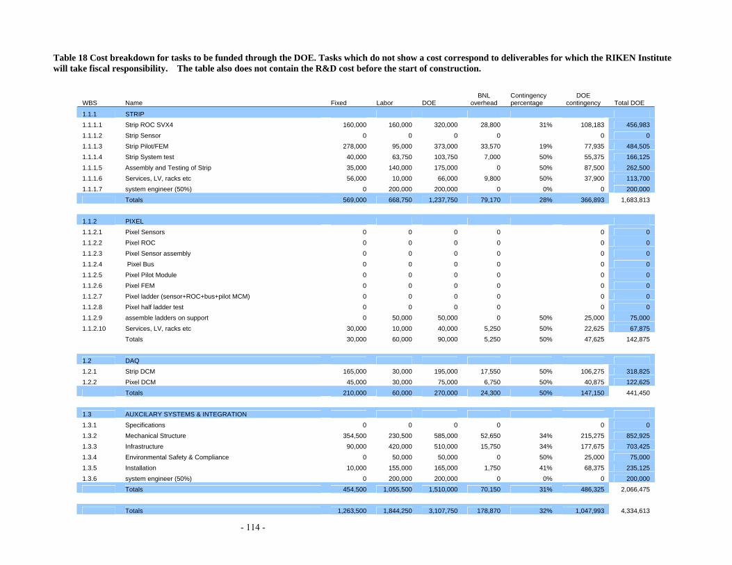
- 114 -
Table 18 Cost breakdown for tasks to be funded through the DOE. Tasks which do not show a cost correspond to deliverables for which the RIKEN Institute will take fiscal responsibility. The table also does not contain the R&D cost before the start of construction.
WBS Name Fixed Labor DOE
BNL overhead
Contingency percentage
DOE contingency Total DOE
1.1.1 STRIP 1.1.1.1 Strip ROC SVX4 160,000 160,000 320,000 28,800 31% 108,183 456,983 1.1.1.2 Strip Sensor 0 0 0 0 0 0 1.1.1.3 Strip Pilot/FEM 278,000 95,000 373,000 33,570 19% 77,935 484,505 1.1.1.4 Strip System test 40,000 63,750 103,750 7,000 50% 55,375 166,125 1.1.1.5 Assembly and Testing of Strip 35,000 140,000 175,000 0 50% 87,500 262,500 1.1.1.6 Services, LV, racks etc 56,000 10,000 66,000 9,800 50% 37,900 113,700 1.1.1.7 system engineer (50%) 0 200,000 200,000 0 0% 0 200,000 Totals 569,000 668,750 1,237,750 79,170 28% 366,893 1,683,813 1.1.2 PIXEL 1.1.2.1 Pixel Sensors 0 0 0 0 0 0 1.1.2.2 Pixel ROC 0 0 0 0 0 0 1.1.2.3 Pixel Sensor assembly 0 0 0 0 0 0 1.1.2.4 Pixel Bus 0 0 0 0 0 0 1.1.2.5 Pixel Pilot Module 0 0 0 0 0 0 1.1.2.6 Pixel FEM 0 0 0 0 0 0 1.1.2.7 Pixel ladder (sensor+ROC+bus+pilot MCM) 0 0 0 0 0 0 1.1.2.8 Pixel half ladder test 0 0 0 0 0 0 1.1.2.9 assemble ladders on support 0 50,000 50,000 0 50% 25,000 75,000 1.1.2.10 Services, LV, racks etc 30,000 10,000 40,000 5,250 50% 22,625 67,875 Totals 30,000 60,000 90,000 5,250 50% 47,625 142,875 1.2 DAQ 1.2.1 Strip DCM 165,000 30,000 195,000 17,550 50% 106,275 318,825 1.2.2 Pixel DCM 45,000 30,000 75,000 6,750 50% 40,875 122,625 Totals 210,000 60,000 270,000 24,300 50% 147,150 441,450 1.3 AUXCILARY SYSTEMS & INTEGRATION 1.3.1 Specifications 0 0 0 0 0 0 1.3.2 Mechanical Structure 354,500 230,500 585,000 52,650 34% 215,275 852,925 1.3.3 Infrastructure 90,000 420,000 510,000 15,750 34% 177,675 703,425 1.3.4 Environmental Safety & Compliance 0 50,000 50,000 0 50% 25,000 75,000 1.3.5 Installation 10,000 155,000 165,000 1,750 41% 68,375 235,125 1.3.6 system engineer (50%) 0 200,000 200,000 0 0% 0 200,000 Totals 454,500 1,055,500 1,510,000 70,150 31% 486,325 2,066,475 Totals 1,263,500 1,844,250 3,107,750 178,870 32% 1,047,993 4,334,613

- 115 -
7.2 Schedule The following plots summarize the construction schedule to complete the VTX detector upgrade for PHENIX. The overall schedule is shown in Figure 69. It assumes start of the DOE construction project in FY05. The subsequent plots, Figure 70 to Figure 72, show the detailed schedule for each major WBS element. The schedule implies that construction dollars from RIKEN are available JFY2003 through JFY2005 and that the DOE construction funds become available in FY06. The schedule after year 2004 is shown. Figure 73 gives the funding profile for the DOE project. In this schedule the inner pixel layer and part of the strip layers will be installed in summer 2006 and the full VTX detector will be completed in summer 2007 shutdown to be ready for RUN8.
Figure 69 The overall schedule for the VTX Project.
Figure 70 The schedule for the strip layers.

- 116 -
Figure 71 The schedule for the pixel layers
Figure 72 The schedule for the auxiliary systems and infrastructure

- 117 -
$0.00
$100,000.00
$200,000.00
$300,000.00
$400,000.00
$500,000.00
$600,000.00
$700,000.00
$800,000.00
Jul-0
5
Aug-05
Sep-05
Oct-05
Nov-05
Dec-05
Jan-0
6
Feb-06
Mar-06
Apr-06
May-06
Jun-0
6Ju
l-06
Aug-06
Sep-06
Oct-06
Nov-06
Dec-06
Jan-0
7
Feb-07
Mar-07
Apr-07
May-07
Jun-0
7Ju
l-07
Aug-07
Sep-07
Oct-07
Cos
t
Total Cost
Figure 73 Budget profile for the VTX project
DOE Construction Costs per Quarter

- 118 -
Appendix A ENDCAP Extension Introduction This section outlines our plans to propose and construct a Silicon Endcap Vertex Detector for PHENIX. The Endcap vertex detector complements the barrel vertex detector by providing larger Bjorken-x coverage, higher total rates and greater reach in transverse momentum. In the following sections, we outline the physics case, specify the requirements, list possible technical options, and define the needed R&D. There are three broad physics topics that are accessible using an Endcap Si vertex detector.
• A large increase in the range of x over which we can extract the gluon spin structure function in protons with measurements of open charm and beauty in polarized p+p reactions.
• Robust measurement of the shadowing of the gluon structure function in nuclei with measurements of open charm and beauty in p+A reactions.
• Probing the early, highest energy-density phase of the matter formed in a heavy-ion reaction using the production of heavy flavor. There are several opportunities:
o Measuring the high-pT spectra of open charm and beauty above 4 GeV/c. The energy-loss of high-pt heavy-quarks is predicted to be less than for lighter-quarks.
o Measuring the yields of both open-charm and beauty in multiple channels to firmly establish whether heavy-quarks are enhanced in the pre-equilibrium phase.
o Using the open charm yield to form the ratio J/ψ/(open charm) and hence to quantify the suppression of J/ψ.
o Identification of upsilon states at rapidity near zero. Our physics goals require that we measure charm and beauty mesons over a broad range of rapidity and transverse momentum. The proposed Endcap vertex detector achieves this by measuring displaced tracks that are matched to the muon arms of PHENIX. A broad pT and rapidity range is achieved by using different decay channels to reach different parts of phase space. The planned upgrade will operate well at 40× design luminosity and many of the measurements need the higher luminosity, e.g. upsilon and open beauty. The proposed detector (VTX) is shown schematically in Figure 1, where there are three distinct parts, a central barrel and two endcaps. The Endcap silicon detectors are designed to provide coverage in the angular acceptance of the forward Muon Arms. They cover 1.2 < |η| <2.7 and the almost full azimuth angle with a resolution of ~150 µm. Each endcap comprises four octagonal “lampshades” populated with Si mini-strip detectors.

- 119 -
Figure 1. Cross-section view of the proposed vertex detector.
Figure 2. A schematic cut-away mechanical drawing of the proposed vertex detector (from Hytec).

- 120 -
A schematic mechanical drawing developed by HYTEC engineering is shown in Figure 2. The proposed detector complements the existing muon arm detectors and significantly enhances the muon physics program.
A.1 Goals of the Endcap Upgrade
A.1.1 Spin Structure of the Nucleon PHENIX has the existing capability shown in Figure 3 as the blue lines. However there are significant gaps in this x-range that will make it difficult to fully address the spin-crisis. The proposed Si Endcap detector extends the coverage to the lowest and highest x-values, 0.001 < x < 0.3, as well as providing significant regions where multiple channels overlap. This overlap will provide vital cross-checks that will improve the reliability of global fits to the spin structure function.
Figure 3. Expected x-range for different channels used to extract the gluon spin structure function. The blue bars indicate PHENIX’s existing capability, green bars are for the Barrel upgrade, while the red bars indicate the additional coverage provided by the proposed Endcap vertex upgrade. The curves show various estimates of the expected gluon polarization.

- 121 -
The Endcap vertex detector provides the following improvements in x-range over a Barrel only detector. These have been estimated by simulating p+p collisions with PYTHIA and requiring sufficient counts in each exit channel to be able to make a reasonable measurement.
• cc production via gluon fusion. The x-range is extended considerably down to x = 0.001 using XD µ→ .
• bb production via gluon fusion. With the upgrade we can identify displaced J/ψ from Ψ→ /JB decay. This provides coverage in x between 0.005 - 0.3. The selection of semi-leptonic decays Xebb µ→ at high momentum is improved using displaced vertices. This extends the xgluon coverage for these semi-leptonic decays to 0.01 - 0.3. Measurement of XB µ→ is also possible by placing a cut on the pT of the muon.
.
A.1.2 Exploration of Gluon Structure in Nuclei The reach in x-range for the Si Endcap is indicated in Figure 4, superimposed on calculations of the ratio of nuclear to nucleon gluon structure function. The red bars indicate the additional coverage provided by the Endcap vertex upgrade compared to the baseline of PHENIX. The Endcap vertex upgrade provides extends the x-range from the anti-shadowing region into the shadowing domain, which means we will be able to establish the shape of the gluon structure function in nuclei. The shadowing region is not accessible with the Barrel-only upgrade. While the x-range for J/ ψ production also extends into the shadowing range, final state effects, such as dissociation, complicate the extraction of the gluon structure function. Open charm and beauty measurements are unaffected by these final state effects.

- 122 -
A.1.3 Probes of Early, Highest Energy-Density Stage of Heavy-ion Reactions Information from the Si Endcap concerning the yield and spectra of heavy-flavor mesons is discussed in the following sub-sections. Of critical importance, is the broad reach in rapidity and transverse momentum made possible by the proposed Endcap upgrade.
Energy Loss of Heavy Quarks Measuring the high-pT (above 4 GeV/c) spectra of open charm and beauty will provide a test of the various theoretical models of energy loss. Since the cross section for these events is low, the large acceptance of the Endcap vertex upgrade versus the Barrel is a distinct advantage.
Open Charm and Beauty Enhancement The Endcap vertex detector, combined with the muon spectrometers, provides excellent rates of open charm and beauty detection. The Endcap upgrade identifies and separates charm and beauty production with high accuracy, even at low pT.
Figure 4. Gluon shadowing predictions along with PHENIX coverage. The red bars indicate the additional range provided by the Endcap vertex upgrade, green bars are for the barrel upgrade, while the blue bars cover the PHENIX baseline. The red and blue curves are theoretical predictions of shadowing from EKS and FKS for different Q values.

- 123 -
J/ψ Suppression To quantitatively understand suppression requires knowledge of the initial production of
cc pairs. The effectiveness of a deconfined medium in preventing the formation of J/ψ can be quantified using the ratio J/ψ/(open charm) in the same acceptance as PHENIX measures J/ψ. The Endcap upgrade provides for the detection of open charm over about the same rapidity interval as for J/ψ decays to dimuons.
Other Physics Topics The Si Endcap vertex upgrade will help other physics programs in PHENIX :
• • The J/ψ resolution in the muon arms will be improved using a vertex detector, from
~150 MeV down to ~100 MeV. This is important for separating the ψ’ from the J/ψ. The physics interpretation is cleaner for the ψ’ than the J/ψ, since it does not have such a large contribution from feeddown of the χc states. Figure 5 demonstrates the improved separation possible with the Si Endcap.
• The signal to background ratio for muon-pairs will be greatly improved by the removal of muons from long-lived pion and kaon decay. This is especially important for pairs with mass below the J/ψ, where the backgrounds are large in nucleus-nucleus collisions.
Figure 5 – Mass spectra for the J/ψ and ψ', showing the substantial improvement in separation expected with a vertex detector (yellow, 100 MeV resolution) compared to that without a vertex detector (black, 150 MeV resolution). The number of J/ψ and ψ’ in this plot represents our expectation for a ~25 pb-1 p+p run.

- 124 -
A.2 Simulations and Required Performance for the Si Endcap Upgrade The performance requirements for the Si Endcap detector are :
• Ability to match tracks from a muon arm to hits in multiple layers of the Si detector. a. Sufficient position accuracy so that the displacement resolution of the track
with respect to the collision point is less than the cτ of charm and beauty decays, i.e. a resolution less than 100µm, preferably at the level of 30 - 50 µm.
b. Good resolution in both rφ and z are required. c. Sufficient segmentation to operate well in Au-Au and high luminosity p+p
collisions. For the simulations we have used two nominal thickness for each layer: 1% and 2% radiation length. This includes detector, readout and cooling in a simplified one-volume effective layer. Our current concept will have a radiation length close to 1% because we are implementing a design that has incorporated a readout bus in the silicon chips and sensors and we are able to thin the chips. We are striving to minimize this thickness, in particular for the critical first disk. The endcaps mini-strips vary in size from 50µm by 2000µm to 50µm by 9000µm as the radius increases. This keeps the occupancy at or below 1.5%.
A.2.1 Open Charm Measurement
Si Endcaps: XD µ→ , eXDD µ→ , XDD −+→ µµ Each silicon endcap detector has four layers of pixel detectors, which measure the trajectory of particles within the nominal rapidity acceptance of the muon arms. The impact parameter of each track is determined accurately along the Z (beam) direction. For each detected muon, the impact parameter is used to eliminate muons that come from pion and kaon decays. These long-lived decays are the primary source of background muons. Contrasted with these background muons are "prompt" single muons, which come from more short-lived decays, e.g. open charm and beauty. For transverse momenta below ~5 GeV/c the prompt muons are primarily from semi-leptonic charm decay. Other processes that produce prompt muons, such as J/ψ or Drell-Yan decays to muon pairs, have much smaller cross-sections times branching ratios. Muons from B decays become important only at larger transverse momenta.

- 125 -
The PYTHIA event generator was used to simulate semi-leptonic charm decays to muons. The total charm pair cross-section was set at 350 µb, which is consistent with recent NLO theoretical calculations and with the published PHENIX measurement at a somewhat lower energy. The decay muons were tracked through the proposed silicon vertex detector and then through the muon spectrometer using PISA. The mean vertex of the detected muons from charm decay is 785 µm from the interaction vertex. This is ~2.5 times larger than the proper decay length of semi-leptonic charm decays (318 µm), due to the Lorentz boost. The impact parameter resolution for these muons ranges from 92 to 115 µm, depending on how many layers of silicon are transversed. By requiring that the muon vertex is within 1cm of the collision point we remove many of the muons from pion and kaon decay while retaining prompt muons from charm and beauty. Figure 6 shows a simulated muon pT spectrum, including charm, beauty and light quark decays, before the application of a vertex cut. The background from light quark decays dominates the spectrum below 4 GeV/c. The pT distribution of muons that survive a 1 cm vertex cut is shown in Figure 7. This vertex cut reduces the muon background from light mesons by about an order of magnitude over what the muon arm alone can achieve, making a charm measurement possible even at low pT. Note that the removal of the muon background from pion and kaon decays could be achieved with a detector with less spatial resolution. The resolution requirement is driven by the physics program of measuring open beauty (see next section).
Figure 6. Single muon pT distributions for charm, beauty and backgrounds from low-mass meson decays, as expected for the 2003 d+Au run. Note that the light-meson decays are above charm up to near 4 GeV/c. The black curve is for pion and kaon decays, green is charm and red is beauty.

- 126 -
To calculate the yield of charm, we assume a 650 µb D pair cross-section, integrated p+p luminosity on tape of 50 pb-1. A total of about 108 semi-leptonic charm decays would be reconstructed. This rate is before application of a vertex or impact parameter cut. Even if a large pre-scale is required for single muon triggers, the yield is still very large. Since charm is produced in pairs, coincidence measurements of opposite-sign lepton pairs may serve to further enhance the signal to noise in p+p and p+A reactions. One could use vertex identified muon-electron coincidences to obtain a clean charm pair signal in the rapidity interval midway between the PHENIX central and muon arms.
A.2.2 Open Beauty Measurement B meson production, while much more rare than D production, is somewhat simpler to measure. The challenge is the relatively low rate. There seem to be at least two possibilities :
• Since beauty mesons have a larger lifetime than charm mesons, it is possible to extract the beauty yield from the distribution of decay distances of single muons
Figure 7. The pT distribution of muons that decay within 1 cm of the collision vertex. The red histogram is for charm decays while the black is for pion and kaon decays.

- 127 -
from semi-leptonic decays. At large transverse momentum beauty decays dominate the DCA distribution.
• The decay channel B J/ψ+X produces J/ψs that are displaced from the collision point.
Si Endcaps: −+→→ µµψ/JB , XB µ→
Applying a vertex cut on each reconstructed J/ψ has been used successfully to identify B-production in experiments at lower energies36. Since the B cross-section is larger at RHIC energies, the measurement should be easier. As the average pT of J/ψ from beauty decays is larger than for prompt J/ψ, a pT cut could also be used to enrich the beauty sample. Pythia was used to simulate −+→→ µµψ/JB decays. The resulting muons are tracked through the silicon and muon spectrometers using PISA. The muons have an impact resolution of ~55 µm, significantly better than muons from D decays, due to their larger average momentum. The pair z-vertex resolution is ~133 µm, while the mean decay length is ~1.1mm. With a downstream pair z-vertex cut of 1 mm, 39% of the B decays are retained, while the prompt J/Ψ are attenuated by a factor of 2x10⁻⁴. Figure 8 shows the reconstructed Z-vertex distribution for the J/ψ from B decays as well as prompt J/ψ.
Figure 8. The reconstructed Z-vertex distribution for J/ψ from B decays (black line) and for prompt J/ψ (red line). Note that the J/ψ yield has been scaled down by a factor of 100. The relative yield of J/ψ from B decays versus prompt J/ψ is estimated to be about 1 %.
J/Ψ /100

- 128 -
We have assumed a total B cross-section of 2 microbarns and 4 microbarns for J/ψ production. The branching ratio of 1.2% for Ψ→ /JB has been previously measured. The total acceptance * BR for these events using two Si Endcaps is ~ 4.0*10-5. Assuming an integrated luminosity to tape of 50 pb-1, about 1900 Ψ→ /JB events would be reconstructed after the application of a 1 mm vertex cut. For XB µ→ , the acceptance * BR is ~ 0.0087. The corresponding yield is ~780,000 reconstructed events. Thus, an excellent B measurement is possible.
A.2.3 Trigger Plans We plan to use the level 1 single and di-muon triggers as the main physics trigger for the Si Endcaps. Higher level triggers could be a level 2 displaced track trigger, possibly similar to the trigger used by CDF and E789. Both CDF and E789 implemented the trigger in hardware to optimize it for speed. For PHENIX this could be ported to level 2. The algorithm for the Si Endcaps / muon spectrometers would be very similar to that done previously by E789. The E789 algorithm functions in three steps (translated into PHENIX language); 1) Muon tracks are found from stubs in the Muon ID and Muon Tracker. The momentum and angle of each track are determined. 2) These tracks are then matched to hits in the Si Endcap using a pre-computed lookup table. 3) Si hits within the matching window are formed into a Si track stub. The stub is then fitted with a straight line to determine the momentum, angle and impact parameter of the track. These events would then be passed to the level 2 triggers of displaced vertexes and/or high-momentum tracks. For pair triggers, tracks could be combined and fitted to determine a pair vertex.
A.2.4 Si Endcap Event Rates The event yields in the previous sections are summarized below. They assume an integrated p+p luminosity on tape (for Run 10) of 50 pb-1. Yields from a comparable Au-Au run would be about a factor of 3X lower. The yields for semileptonic heavy quark decays are about an order of magnitude larger than for the Si Barrel, due to the larger acceptance of the Si Endcap. The B decay rates could benefit from the increased luminosity in the RHIC II proposal.
Observable Counts per RHIC p+p Run 10 XD µ→ ~ 108 XB µ→ 780k
−+→Ψ→ µµXJB / 1900

- 129 -
A.2.5 Matching to Muon Spectrometers Track matching between the Si Endcaps and the Muon Spectrometers was studied by using hijing Au-Au central collisions in a PISA simulation. A muon track was embedded in a hijing event. The muon track was found in station 1 from the muon tracker by demanding that the muon reached the middle of the MUID, i.e. the muon energy was > 2.5 GeV. The distribution of the muon hits in station 1 was found to be +- 2 cm from the projection of the Si Endcap track, due to multiple scattering in the central magnet steel. No other track in the tracker was found to be in a +- 2cm cut around the muon hit in station 1. We then looked for all tracks in the Si Endcaps that had their projection fall into the 2 cm cut about the muon track. In addition to the muon, typically 3 other tracks fell into this cut. Of these candidate tracks all except the muon came from the primary interaction vertex. The background would be the fraction of primary tracks that fall beyond a 1 mm cut.
A.2.6 Integration with PHENIX The proposed Endcap vertex detector matches and extends the capability of the existing muon spectrometer arms. In addition a TPC is being proposed to sit outside the vertex detector. The Detector Advisory Committee recommended studies exploring the impact of the VTX on the TPC with the possibility of standalone running for either detector. Because the Endcaps are outside of the acceptance of the HBD/TPC we believe that both detectors can operate simultaneously.
A.3 Technical Aspects of the Proposed Endcap Vertex Detector
A.3.1 Silicon Readout Chip –PHX FNAL Electrical Engineering Department, ASIC development group (Group leader, Ray Yarema) has designed the FPIX2 chip, a low-noise programmable Si pixel readout chip for the planned BTeV experiment. The chip is an advanced mixed analog/digital DC-coupled design optimized for a detector with 50 µm by 400 µm pixels. The device has very low noise (60 electrons RMS) and high-speed readout, including the ability to interface to a level 1 type trigger. Approximately 3000 FPIX2 chips have been produced in an engineering run, with a high yield of fully functional devices. Test results are very encouraging, with the prototypes demonstrating excellent performance and minimal cross-talk. Only minor design tweaks are needed before a production run of the devices could be made. The electrical design of the FPIX2 chip is similar to that needed for the Si Endcap pixels. The main change required is to adapt the physical chip geometry to accommodate the Endcap sensors larger mini-strips. These modifications are not very difficult, with an

- 130 -
estimate of 2 man-years. Yarema has offered the services of his engineers and facilities to perform this work. They have already completed a conceptual layout of the modified PHX readout chip, which is shown in Figure 9. This elegant design has the readout bus structure integrated into the chip itself, simplifying the sensor-readout assembly process. The PHX chip will be bump-bonded to the sensor, with 200 µm bump spacing. This relatively large spacing was chosen to ensure high yields during the assembly process. Yarema’s team have also simulated the FPIX2 response with input capacitances corresponding to our larger mini-strips and found it to be acceptable. The schedule and R&D budget for the PHX chip development are given in section 6.4 below. These were provided to us by Ray Yarema. Approximately two years are need to complete all of R&D related to the PHX chip.
A.3.2 Silicon Ministrip Sensors We plan on using existing technology for the silicon sensor. Pixel Sensor technology from the either the ALICE, ATLAS or CMS efforts will have the pixel layout (masks) modified to match the longer mini-strips that we need. Developing the masks for this effort will be done in concert with the vendors of the sensors. Lengthy and costly R&D for the sensors is not necessary. Three different silicon sensors of trapezoidal shape are used to tile the active areas of the Si Endcap, as shown in Figure 10. Also shown is the arrangement of the readout chips on each of the sensors. The largest sensor is 79 mm high and 27 mm wide at its large end. Six PHX chips are used to readout the 3072 mini-strips. The smaller sensors contain 2560 and 1536 strips.

- 131 -
Figure 9: Conceptual layout of the PHX pixel readout chip. The left side graphic depicts the general layout of the chip. Green is the area for bonding, blue the programming interface, red the discriminator, orange the pipeline and yellow the digital interface. The right side graphic shows the bonding layout, the spacing is 200 micron. The signal and power bus will be routed on the surface on the chip and bonded via the bump bonds on the ends of the chip.
The Si Endcap detector layers are assembled as shown in Figures 11 through 13. First, the sensors are tiled on carbon panels that serve as the support and cooling structure for each of the sector assemblies (Figure 11). Next, 24 sectors are joined to form each of the four z-Stations (Figure 12). Finally, the four z-Stations are assembled in each Si Endcap detector (Figure 13). Each Endcap contains approximately two million strips.

- 132 -
Figure 10: Three silicon detectors will be used. The largest will have 6 chips reading out 3072 strips, the intermediate silicon will have 5 chips reading out 2560 strips and the smallest silicon is half the size of the largest with 3 chips reading out 1536 strips. (All dimensions are in millimeter)
Figure 11: A sector assembly will have 24 carbon panels (one shown here in brown) in azimuth, each of them carrying 4 silicon detectors (blue), two in the front and two in the back. They overlap on the edges by a few millimeters to avoid dead areas. The bus on a silicon assembly is routed on the chips as described earlier, the connection of the inner silicon detectors is realized via a kapton bus (golden).

- 133 -
Figure 12: Each station carries 96 silicon detectors. The stations are placed at ~20, 26, 32 and 38 cm from the interaction point.
Figure 13: Each endcap will have 4 stations of silicon detectors. The inner station has a reduced size in order to not interfere with the HBD acceptance.

- 134 -
A.3.3 Silicon Ministrip Control Chip The Control Chip serves as a receiver for the PHX chip digital output and is located at the outer edge of each sector. It formats the data to be compatible with the PHENIX DCMs, converts the data into serial form and drives a 2.5 gigabit/sec fiber. The other end of the fiber connects to the DCM in the counting house. It is simpler than the PILOT chip used to interface the Si barrel, as it does not need to combine separate data streams to meet PHENIX’s DAQ speed requirements. (The PHX chip is already fast enough for PHENIX). We envision that the Control Chip would consist of an FPGA plus a laser diode and driver. The University of Heidelberg has expressed interest in developing the Control Chip with us.
A.3.4 Mechanical Structure and Cooling The mechanical structures and cooling are part of the integrated design discussed in Chapter 4. The majority of the support structure will be designed as part of the barrel effort and remaining issues concerning ladders and cooling specific to the endcaps will be discussed here.
A.3.5 Endcap Ladder Structure The forward regions consist of 4 conical arrays of ladder modules tilted from the normal to the beam pipe by 22 deg. Conceptually, we have chosen a flat octagonal panel structure with sensors and electronics mounted on either side of the panel so that we can achieve hermetic coverage. Figure 14 shows this arrangement on the left and an octagon panel structure on the right.
Figure 14. 3D model of octagonal disk like structures for the endcap ministrips. Cooling tubes are shown to demonstrate both the number and routing. The octagon panel structure is on the right with the cooling channel shown. A heat load of 0.1 W/cm**2 is assumed.

- 135 -
Each endcap has a total heat load of approximately 450W, or about 15W per octant panel. In comparison to the barrel this is a very small heat load and greatly simplifies the removal of the waste heat. The octant panel structure consists of a composite sandwich of C_C facings on either side of a carbon foam in which is embedded an aluminum cooling tube( Figure 15). Thermal and gravity sag calculations were performed in a manner similar to those discussed in chapter 4 and no serious distortions were observed. For the case of 0 deg operation, more work is necessary.
Figure 15. Illustration of an embedded cooling passage arrangement in the composite sandwich used in the endcap thermal and static calculations. The upper panel depicts a circular tube with supports and the bottom panel shows a flattened tube which enhances heat transfer and provides a thinner sandwich.
A.3.6 Radiation Length The thermal and static design studies produced a range of solutions for the endcaps Figure 16 shows the radiation length estimate for different cooling tube dimensions. The parameters used in the calculations are:
• Al tube, 200 micron. • 4 mm carbon foam separator. • Tube support 2 mm wider than tube diameter. • Sandwich facings of 400 micron.
Figure 16. Estimated normal radiation length for the endcap octant panel for different tube diameters.

- 136 -
6.3.7 Endcap Analysis Summary
The conceptual design studies revealed the following:
• Single phase cooling is well suited to the endcaps. • Two adjacent octant panels can be cooled in series thus reducing service
connections. • 2mm cooling tubes and panel thickness are adequate. • The radiation length of the octant panel exclusive of sensor and electronics is ~
0.6 %. The R&D issues consist of refining the calculations, designing attachment points to the main support structure, and prototyping the octant panels.
A.4 R+D Schedule, Responsibilities and Budget
A.4.1 Schedule The R+D schedule for project 2 is shown below. Also shown is a construction and installation schedule assuming funds are available now. This will slide with funds availablity. The R+D is expected to begin in early FY05 and be completed by late FY06.
- 137 -
A.4.2 Responsibilities The LANL Group will work together with HYTEC inc. to develop the design for the Endcap mechnical ladder and cooling. LANL has formed collaboration with FNAL to design, prototype and test the PHX readout chip. An MOU among PHENIX, BNL physics department and FNAL for R&D of the PHX chip was signed in 2004.
1 K. Adcox et al., Phys. Rev. Lett. 88, 19203 (2002) 2 E. Shuryak Phys. Rep 61, 71 (1980) 3 P. Levai et al, Phys. Rev C. 51, 3326 (1995) 4 Z. Lin and M. Gyulassy, Phys. Rev. C. 51, 2177 (1995) 5 R. Baier, D. Schiff, B.G. Zakharov, Ann. Rev. Nucl. Sci 50, 37 (2000) 6 U.A. Wiedemann, Nucl. Phys. B 588, 303 (2000) 7 M. Gyulassy et al., nucl-th/0006010 8 Yuri L. Dokshitzer, D.E. Kharzeev Phys.Lett.B519:199-206,2001 9 M. Djordjevic, M. Gyulassy nucl-th/0305062 10 M. Djordjevic, M. Gyulassy, Phys. Lett. B.560, 37 (2003) 11 B. H. Zhang, E. Wang, X-N. Wang, nucl-th/0309040 12 S. Batsouli, et al, Phys. Lett. B557, 26 (2003) 13 M.C. Abreu et al (NA50), Phys. Lett. B410, 327 (1997). 14 B.Z. Kopeliovich, A.V. Tarasov, Nucl. Phys. A710, 180 (2002) or hep-ph/0205151 and J. Raufeisen private communication. 15 L. Grandchamp and R. Rapp, Phys. Lett. B523, 60 (2001). 16 A. Andronic et al., Phys Letters B571, 36 (2003) 17 R.L.Thews, et al., Phys. Rev. C63, 054905(2001) 18 C.Lourenco, “Workshop on Quarkonium Production in Relativistic Nuclear Collisions”, Seattle, 11 May 1998, B-> J/Psi estimates, private communication. 19 R. Rapp, nucl-th/0204003 20 M. Arnedo, Phys. Rep. 240, 301 (1994), K.J. Eskola et al., hep-ph/9906484. 21 L. McLerran and R. Venugopalan, Phys. Rev. D49, 2233 (1994); A.H. Mueller and J.W. Qui, Nucl. Phys. B 268 427 (1986) and L.V. Bribox, E.M. Levin and M.G. Ryskin, Phys. Rept. 100, 1 (1983). 22 L. Frankfurt, M. Strikman, Eur. Phys. J A5, 293 (99) 23 B.Z. Kopeliovich, A.V. Tarasov, J. Huefner, Nucl. Phys. A696, 669 (2001) or hep-ph/0104256. 24 K.J. Eskola, V.J. Kolhinen and R. Vogt, Nucl. Phys. A696, 729 (2001) or hep-ph/0104124. 25 D. Kharzeev, Nucl. Phys. A702, 39 (2002) or hep-ph/0111386. 26 L. Frankfurt, M. Strikman, Eur. Phys. J A5, 293 (99) 27 M.A. Vasiliev et al (E866/NuSea), Phys. Rev. Lett. 83, 2304 (1999). 28 Heijne, E.H.M., Nucl. Instrum. Methods Phys. Res. A465 (2001) 1-26 29 W. Snoeys et al., Nucl. Instr. Meth. Phys. Res. A465 (2001), 176; K. Wyllie et al., Proc. Fifth Workshop on Electronics for LHC Experiments, Snowmass, Colorado, 1999. 30 NA60 Collaboration, CERN/SPSC 2000-010, March 2000; 31 Jorma Salmi and Jaakko Salonen, VTT, Finland, Workshop on Bonding and Die Attach Technologies CERN, Geneva, Switzerland, June 11-12, 2003, http://ssd-rd.web.cern.ch/ssd-rd/bond/talks/1-04_Salmi.pdf 32 P. Riedler, CERN, Workshop on Bonding and Die Attach Technologies CERN, Geneva, Switzerland, June 11-12, 2003, http://ssd-rd.web.cern.ch/ssd-rd/bond/talks/2-01_Riedler.pdf 33 J.M. Heuser et al. (NA60 Collaboration), Proceedings of the Conference on the Intersections of Particle and Nuclear Physics, New York City, May 19-24, 2003, American Institute of Physics Conference Proceedings 698 (2003) 713-717

- 138 -
34 V. Eremin et al., Nucl. Instr. and Meth. A 372, 388 (1996). 35 Ideas ASA (Norway), http://www.ideas.no/ 36 E789 Phys. Rev. Lett. 74, 3118 (1995).