proposed modifications to engineering design …
TRANSCRIPT

1
PROPOSED MODIFICATIONS TO ENGINEERING DESIGN GUIDELINES RELATED TO RESISTIVITY MEASUREMENTS AND SPACECRAFT CHARGING
J.R. Dennison, Prasanna Swaminathan, Randy Jost and Jerilyn Brunson Physics and Electrical and Computer Engineering Departments, Utah State University
SER 250 UMC 4415, Logan, UT, USA 84322-4415 Phone: 435.797.2936, Fax: 435.797.2492, [email protected]
Nelson W. Green and A. Robb Frederickson
Jet Propulsion Laboratory, California Institute of Technology 4800 Oak Grove Drive, Pasadena CA 91109-8099
Phone: 818.393.6323, Fax: 818.393.0351, [email protected]
Abstract
A key parameter in modeling differential spacecraft charging is the resistivity of insulating materials. This parameter determines how charge will accumulate and redistribute across the spacecraft, as well as the time scale for charge transport and dissipation. Existing spacecraft charging guidelines recommend use of tests and imported resistivity data from handbooks that are based principally upon ASTM methods that are more applicable to classical ground conditions and designed for problems associated with power loss through the dielectric, than for how long charge can be stored on an insulator. These data have been found to underestimate charging effects by one to four orders of magnitude for spacecraft charging applications.
A review is presented of methods to measure the resistivity of highly insulating materials—including the electrometer-resistance method, the electrometer-constant voltage method, the voltage rate-of-change method and the charge storage method. This review is based on joint experimental studies conducted for NASA at the Jet Propulsion Laboratory and at Utah State University to investigate the charge storage method and its relation to spacecraft charging. The different methods are found to be appropriate for different resistivity ranges and for different charging circumstances. A simple physics-based model of these methods allows separation of the polarization current and dark current components from long duration measurements of resistivity over day- to month-long time scales. Model parameters are directly related to the magnitude of charge transfer and storage and the rate of charge transport. The model largely explains the observed differences in resistivity found using the different methods and provides a framework for recommendations for the appropriate test method for spacecraft materials with different resistivities and applications. The proposed changes to the existing engineering guidelines are intended to provide design engineers more appropriate methods for consideration and measurements of resistivity for many typical spacecraft charging scenarios.
Introduction The central theme of the 9th Spacecraft Charging Conference has been how spacecraft interact with the plasma environment to cause charging. This paper focuses on resistivity of insulators and its relation to spacecraft charging. Specifically, we will focus on understanding what materials properties to measure, how best to measure them, and how to understand these properties in the context of spacecraft charging [1]. We also present suggested modifications to make to new spacecraft charging guidelines as related to resistivity measurements of good insulators [2]. Spacecraft accumulate charge and adopt potentials in response to interactions with the plasma environment. A key parameter in modeling differential spacecraft charging is the resistivity of insulating materials. This determines how charge will accumulate and redistribute across the spacecraft, as well as the time scale for charge transport and dissipation. Existing spacecraft charging guidelines [3,4] recommend use of standard resistivity tests and imported resistivity data from handbooks that are based principally upon ASTM methods [5,6] that are more applicable to classical ground conditions and designed for problems associated with power loss through the dielectric, than for how long charge can be stored on an insulator. These data have been found to underestimate charging effects by one to four orders of magnitude for spacecraft charging applications [7-10]. Classical methods to measure thin film insulator resistivity use a parallel plate capacitor method to determine the conductivity of insulators by applying a constant E-field (voltage). The presence of two conducting surfaces, the charge and E-field profile, and the charge injection method differ from typical spacecraft scenarios. Also, the classical methods fail to fully take into consideration the fact that resistivity continues to change over long time periods as the material responds to the applied electric field and the accumulated charge distribution. Constant voltage and similar

2
standard methods rely on electrometer measurements of current, voltage or resistance. They have been found to often be instrumentation resolution limited to accurate measurements of resistivities of less than 1012 to 1017 Ω-cm [1,5,11]. Inconsistencies in sample humidity, sample temperature, initial voltages and other factors from such tests cause significant variability in results [5]. Further, the duration of standard tests are short enough that the primary currents used to determine resistivity are often caused by the polarization of molecules by the applied electric field rather than by charge transport through the bulk of the dielectric [1,7,8]. Testing over much longer periods of time in a well-controlled vacuum environment is required to allow this polarization current to become small so that accurate observation of the more relevant charged particle transport through a dielectric material is possible. We concluded then that the classical resistivity method may not be most appropriate test method for spacecraft charging problem [1,12]. The charge storage method was developed by Frederickson et al. [7,8,13-16], Levy et al. [17-19] and others [20,21] to measure the resistivity in a more applicable configuration. In this method, charge is deposited near the surface of an insulator and allowed to migrate through the dielectric to a grounded conductor. Charge storage resistivity tests have now been done for Polyimides, Mylar, Teflon, Glass, Circuit Boards, and other common spacecraft materials [7-9]. The study by Green et al. [9] in these proceedings describes a charge storage study of selected samples remaining from the Internal Discharge Monitor (IDM) experiment on the CRRES satellite [13,15,22,23]. The sample set on CRRES was chosen to cover a range of dark current resistivity values and polarization magnitudes and rates. Hence, the set provides an excellent test bed for both the charge storage method of resistivity measurements and the behavior of dielectrics in the space environment. In this paper, we present a simple physics-based model to describe the different test methods used to measure resistivity of highly insulating materials. The model allows separation of the polarization current and dark current components from long duration measurements of resistivity over day- to month-long time scales. Model parameters are directly related to the magnitude of charge transfer and charge storage and to the rate of charge transport. The model largely explains the observed differences in measured resistivity found using the different methods and provides a framework for recommendations for the most appropriate test methods for spacecraft materials for a wide range of resistivities and applications. Model of Capacitor Charging and Discharge The proposed model is developed from very basic principles—Gauss’ Law and the constitutive relation of macroscopic electric fields, the definitions of basic materials properties including resistivity and dielectric constant, and a few assumptions about sample geometries and conditions. Readers are familiar with concept of resistance as the proportionality constant in Ohm’s Law: R = V / I. R is an extrinsic property that measures the resistance to flow of electric current, I, for an electromotive driving force (voltage), V, for a particular electrical component (see Figure 1a). Resistivity, ρ, is the proportionality constant in another form of Ohm’s Law, ρ = E / J, where E is the electric field and J is the electric current density. From these two forms of Ohm’s Law, it is evident that ρ = R · A/L ≡ 1 / σ, where A is the cross-sectional area of the resistor, L is the length of the resistor and σ is the conductivity (refer to Figure 1b). A key advantage to the use of resistivity is that ρ is an intrinsic material property that does not depend on the amount of material in a specific sample or on its geometry. For most resistivity test methods, the highly insulating samples can be treated as simple parallel plate capacitors. This simple model is also applicable to most spacecraft charging situations encountered in both surface charging of exterior insulating coatings and charging of insulators in the interior of spacecraft. Almost all charge resulting from space environment interactions is deposited within microns of the surface (except for relatively rare very high energy
Figure 1. (a) Schematic of circuit defining the resistance Rx of a device X in terms of a source voltage Vs and a current I through Ohm’s Law, Rx=Vs/I. (b) Sample dimensions used to define the resistivity ρ x =Rx·A/d, in terms of the length L and the cross sectional area A=h·w.
(b)
(a)

3
incident particles) and can travel only short distances in highly insulating materials that present the major problems in spacecraft charging. These spacecraft elements typically have lateral dimensions on the order of mm to meters. Thus, most dielectrics of concern can be considered thin-film dielectrics. Even for interior or deep dielectric charging resulting from high energy incident particles that can penetrate further into the spacecraft and interact with improperly shielded dielectrics (e.g., cable insulation, printed circuit board insulation, or insulating stand-offs), the charge is typically deposited over a fairly narrow depth range and does not migrate large distances; thus, this too can be reasonably approximated in most cases as a thin film-dielectric. Charge deposited in the thin-film insulators typically dissipates through the insulator to a conducting substrate. Therefore, thin-film parallel plate capacitors are usually good models of both dielectrics measured with standard resistivity test methods and for those of concern in spacecraft charging. The behavior of charge accumulation and dissipation on a parallel-plate capacitor is well known. Voltage (or charge) decay depends exponentially on time, t, with decay constant, τ, through a relation for surface voltage or charge density V(t)=Voe-t/τ or σ(t)= σoe-t/τ , with τ=R•C=ε•ρ, (1)
Figure 2. Resistivity can be measured using the simple RC time constant method. (a) Simple thin film capacitor sample geometry with thickness d, surface area A, permittivity ε, and resistivity ρ=R•A/d, where R is the sample resistance. (b) Schematic of a simple RC test circuit with sample capacitance C and resistance R of a sample with surface voltage V(t)=Voe-t/τ as a result of stored charge σ(t)= σoe-t/τ. (c) A typical decay curve of sample voltage as a function of time, t, with time constant τ=R•C=ε•ρ. (d) Schematic of Capacitor (Constant Voltage) Resistivity Test Circuit. (e) Schematic of Charge Storage Resistivity Test Circuit.
(a) (b) (c)
(d) (e)

4
where Vo and σo are the initial voltage or charge density, respectively. A typical decay curve of sample voltage as a function of time t with time constant τ=R•C=ε•ρ is shown in Figure 2c [3]. The decay constant for a specific sample can be expressed in terms of the two extrinsic properties R and C, where R is the resistance of the dielectric across the capacitor and the capacitance of the thin-film parallel plate capacitor, C= εo εr A/d, where εo=8.854·10-12 F/m is the permittivity of free space, ε is the permittivity in a dielectric medium, and εr≡ ε/εo is the relative permittivity. Alternately, the decay constant for a given material can be expressed as the product of the resistivity and the dielectric constant. Resistivity is a measure of how fast free charge applied to the capacitor will dissipate by migrating through the dielectric. The dielectric constant describes the response of the material to the electric field inside the capacitor; that is, the change in relative dielectric constant is the ratio of the bound charge on the capacitor plates (equal to the polarization field of the dipoles within the dielectric generated in response to the electric field produced by the free charge) to the free charge. In terms of charge density on the capacitor plates,
Free
Boundr
Free
Totalr
σ
σε
σ
σε
==−
==
density charge freedensity charge bound)1(
density charge freedensity charge total (2)
The dielectric constant and the electric flux density, D, are defined through the constitutive relation for the macroscopic electric field as PEEED oro +=== εεεε (3) Figure 3 illustrates two situations, when the material between the capacitor plates is unpolarized (εr=1) and when it is polarized (εr>1). The polarization P=(εr -1)εoE is a field that results from the response of the medium to an applied electric field, E, and can be thought of as due to the alignment of the dipoles within the dielectric material to the electric field E. The constitutive relation, Eq. 3, together with a statement of charge conservation, Boundσσσ += FreeTotal , leads to expressions for the charges defined only in terms of the E-field and the free charge dependant macroscopic material parameter εr:
PE
E
DE
or
o
orTotal
≡−=
=
≡=
εεσ
εσ
εεσ
)1(Bound
Free
(4)
where of the actual total charge density on the capacitor plates σTotal, only a fraction of the charge density σFree contributes to the neutralization of the voltage on the plates and the remainder of the charge density σBound is bound charge neutralized by the polarization of the dielectric material. Thus, any time dependence in charge must follow from time dependence in either σFree (t)= εo E(t) or from εr(t).
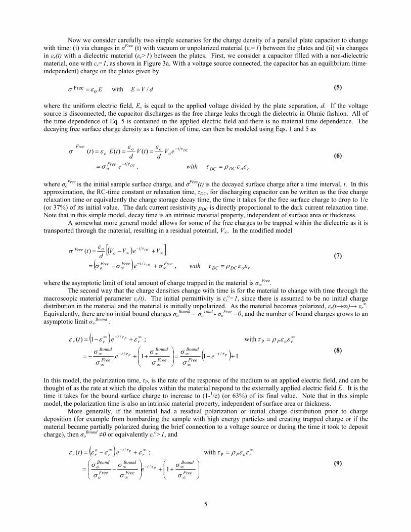
Figure 3. Charge distribution of a parallel plate capacitor connected to a constant voltage source, V (a) with vacuum or unpolarized material (εr=1) between the plates and (b) with a dielectric material (εr>1) between the plates.
5
Now we consider carefully two simple scenarios for the charge density of a parallel plate capacitor to change with time: (i) via changes in σFree (t) with vacuum or unpolarized material (εr=1) between the plates and (ii) via changes in εr(t) with a dielectric material (εr>1) between the plates. First, we consider a capacitor filled with a non-dielectric material, one with εr=1, as shown in Figure 3a. With a voltage source connected, the capacitor has an equilibrium (time-independent) charge on the plates given by dVEEo / withFree == εσ (5) where the uniform electric field, E, is equal to the applied voltage divided by the plate separation, d. If the voltage source is disconnected, the capacitor discharges as the free charge leaks through the dielectric in Ohmic fashion. All of the time dependence of Eq. 5 is contained in the applied electric field and there is no material time dependence. The decaying free surface charge density as a function of time, can then be modeled using Eqs. 1 and 5 as
roDCDCtFree
o
to
ooo
Free
withe
eVd
tVd
tEt
DC
DC
εερτσ
εεεσ
τ
τ
==
===
−
−
,
)()()( (6)
where σo
Free is the initial sample surface charge, and σFree(t) is the decayed surface charge after a time interval, t. In this
approximation, the RC-time constant or relaxation time, τDC, for discharging capacitor can be written as the free charge relaxation time or equivalently the charge storage decay time, the time it takes for the free surface charge to drop to 1/e (or 37%) of its initial value. The dark current resistivity ρDC is directly proportional to the dark current relaxation time. Note that in this simple model, decay time is an intrinsic material property, independent of surface area or thickness. A somewhat more general model allows for some of the free charges to be trapped within the dielectric as it is transported through the material, resulting in a residual potential, V∞. In the modified model
( )[ ]( ) roDCDC
FreetFreeFreeo
to
oFree
withe
VeVVd
t
DC
DC
εερτσσσ
εσ
τ
τ
=+−=
+−=
∞−
∞
∞−
∞
,
)(
/ (7)
where the asymptotic limit of total amount of charge trapped in the material is σ∞Free. The second way that the charge densities change with time is for the material to change with time through the macroscopic material parameter εr(t). The initial permittivity is εr
o=1, since there is assumed to be no initial charge distribution in the material and the material is initially unpolarized. As the material becomes polarized, εr(t→∞)→ εr
∞. Equivalently, there are no initial bound charges σo
Bound = σoTotal - σo
Free =0, and the number of bound charges grows to an asymptotic limit σ∞Bound :
( )( ) 111
with ;1)(
//
P/
+−=
++−=
=+−=
−
∞
∞
∞
∞−
∞
∞
∞∞−∞
PP
P
tFree
Bound
Free
Boundt
Free
BoundroPr
trr
ee
et
ττ
τ
σσ
σσ
σσ
εερτεεε
(8)
In this model, the polarization time, τP, is the rate of the response of the medium to an applied electric field, and can be thought of as the rate at which the dipoles within the material respond to the externally applied electric field E. It is the time it takes for the bound surface charge to increase to (1-1/e) (or 63%) of its final value. Note that in this simple model, the polarization time is also an intrinsic material property, independent of surface area or thickness.
More generally, if the material had a residual polarization or initial charge distribution prior to charge deposition (for example from bombarding the sample with high energy particles and creating trapped charge or if the material became partially polarized during the brief connection to a voltage source or during the time it took to deposit charge), then σo
Bound ≠0 or equivalently εro>1, and
( )
++
−=
=+−=
∞
∞−
∞
∞
∞∞−∞
Free
Boundt
Free
Bound
Freeo
Boundo
roPrt
rorr
P
P
e
et
σσ
σσ
σσ
εερτεεεε
τ
τ
1
with ;)(
/
P/
(9)

6
Model of Resistivity Test Methods We are now ready to develop models for two methods of measuring the resistivity considered below, the Electrometer—Constant Voltage Method and the Charge Storage Decay Method. More detailed discussions of these and additional resistivity test methods are found in references 1, 5, and 11. Electrometer—Constant Voltage Resistivity Test Method
In this method, a constant voltage is applied to two parallel plate capacitors with the dielectric test sample between the plates, and the current from the supply is monitored with and electrometer (see Figure 2d). If the capacitor plate voltage is held constant at VCV, the electric field, ECV=VCV/d, is also constant. The capacitor will be charged such that the free charges on each plate produce a potential difference equal and opposite to the fixed voltage,
dVCVoFreeCV εσ = , as illustrated in Figure 3a The time-dependant total charge, from Eq. 4a is then
( )[ ]
( ) ( )BoundFreeCV
tBoundBoundo
roPrt
ror
CVoCVro
TotalCV
P
P
e
edV
Ett
∞−
∞
∞∞−∞
++−=
=+−==
σσσσ
εερτεεεε
εεσ
τ
τ
/
P/ with ;)()(
(9)
The polarization current is then given by ( )
P
P
t
P
orr
oCV
tBoundo
Bound
P
TotalCV
P
eCV
eAdt
tdAtI
τ
τ
τεε
σστ
σ
/
/)()(
−∞
−∞
−=
−== (10)
where A is the area of the sample and the free air capacitance of the sample is Co=εoA/d. The current to the plates from the voltage source is the sum of two components, the polarization current and the leakage current, where
DC
roCV
DCo
oCV
DC
CVLeak CV
CVd
AVI
τε
ρερ
∞
=
=
=
11 (11)
Here, the dark current conductivity, ρDC, is assumed to be a constant, independent of time and ECV (or equivalently VCV). Combining Eqs. 10 and 11, the total current as a function of time is
+
−=+=
∞−
∞∞
DCrt
P
orr
oCVLeakPDCPorr PeCVItItI
τε
τεεττεε τ/
CV )(),,,;( (12)
If there is no initial polarization, εr
o=1. In the limit of short time, with τDC»τP and εro=1,
Pt
Pr
oCVoPPr eCVtItI τ
τετε /o
CV1)(),;( −
∞∞
−=→
(13)
In the limit of long time, with τDC»τP and εr
o=1, the current approaches an asymptotic limit equal to only the leakage current
=→
∞∞∞
DCroCV
LeakDCrCVCVItI
τετε ),;(
(14)
Charge Storage Decay Resistivity Test Method
In this method, an initial charge σoTotal is deposited on the sample surface. This can result from the direct
deposition of charge as is the case for the charge storage decay method or from the connection of a voltage source which is subsequently removed as is the case of the voltage rate-of-change method. The surface charge is then

7
monitored using a non-contact electric field probe, as σFree(t) is allowed to discharge through the thin-film dielectric to an underlying grounded conductor and σBound(t) develops in response to the electric field generated by σFree(t). The capacitor plate voltage as a function of time that results from a deposited surface charge density σo
Total(t), using Eqs. 4 and 5 is
)()()()(t
dtdttVro
Free
o
TotalCS εε
σε
σ==
(15)
Note that the time evolution of the charge storage voltage depends on both the charge dissipation σFree(t) via the dark current resistivity and the evolving polarization of the dielectric through εr(t). Inserting the results of Eqs. 7 and 9, we find
( )
++
−
+−=
∞
∞−
∞
∞
∞−
∞∞∞
Free
Boundt
Free
Bound
Freeo
Boundo
FreetFreeFreeo
oDCP
BoundBoundo
FreeFreeoCS
P
DC
e
edtV
σ
σ
σ
σ
σ
σ
σσσε
ττσσσστ
τ
1
),,,,,;(/
/
(16)
roDCDCwith εερτ =, or in terms of the initial and final voltages and permittivities,
( )[ ]( ) roDCDC
rt
ror
to
ProroCS with
e
VeVVVVtVP
DC
DC εερτεεε
ττεε τ
τ=
+−
+−=
∞−∞∞
−∞∞
∞ ,),,,,;( /, (17)
If there is no initial polarization, εro=1. If there are no free charges trapped within the dielectric as it is
transported through the material and t→∞, then this results in a residual potential, V∞=0. In the limit of short time, with τDC»τP and εr
o=1, ( )[ ] 1/1),,;(
−−∞∞∞ −+→ PtrroPro
oCS eVVtV τεετε (18)
In the limit of long time, with τDC»τP, εr
o=1 and V∞=0, DCt
oDCoCS eVVtV ττ −∞ →),;( (19) Comparison of Resistivity Test Method Resolutions
Determination of resistivity for materials can be a difficult process, complicated by both instrumentation and procedural methods and by external conditions that are difficult to control but that can have very large effects on the test results. This section provides a discussion of four commonly accepted resistivity test procedures, with an emphasis on their resolution and valid range of applicability (refer to Table I for a summary), as they relate to the simple physics-based theory presented above. We assume in this section that the test apparatus and methods are well designed to minimize problems from sample contamination, temperature, humidity, vibration, electromagnetic interference, dielectric breakdown and other confounding variables. Further details can be found in Test Protocol for Charge Storage Methods [1], that describes in detail test apparatus, measurement methods and analysis techniques for these and other resistivity test methods appropriate for high resistivity insulators used in space applications.
Recommended test procedures and instrumentation for multimeter and electrometer test methods are described in test procedures standards [5,6] and also in standard references such as [11] and [24]. A thorough discussion of environmental conditions and their effects on the precision and accuracy of resistivity measurements using electrometer methods is given in Appendix X1 of ASTM D-257-91 [5] and also in standard references such as [11] and [12]. ASTM Standard 618 [25] provides recommendations for sample conditioning prior to the measurements.
Digital Multimeter Method
Standard digital multimeters use an internal voltage source to determine resistance. The method is usually
limited by the internal resistance of the meter, which typically does not exceed ~1010 Ω for a very good multimeter [11]. Multimeters are typically useful in measuring resistivity no higher than ~1012 Ω·cm. Such resistivities correspond to a

8
longest measurable decay time of ~0.1 sec. As such, resistivity measurements with multimeter are not useful for measuring resistivity of materials likely to cause charging problems in spacecraft applications. Electrometer in Resistance Mode Method
Standard digital electrometers operating in a stand alone resistance mode also use an internal voltage or current source to determine resistance, but have higher resolution than digital multimeters. Measurements of current with a constant-voltage source are the preferred method [11]. Measurements at this level require very good electrometers and careful attention to the test circuit and sample preparation. The method is limited by the sensitivity of the resistance meter, which typically does not exceed ~1016 Ω for a very good electrometer [11]. Electrometers in a resistance mode with ideal test fixtures are useful in measuring resistivity no higher than ~1016 Ω·cm. Such resistivities correspond to a longest measurable decay time of ~45 min. Limitations of the test facilities or electrometers typically limit measurements with digital electrometers operating in a stand alone resistance mode to one or two orders of magnitude less resistivity or decay times, on the order of <1015 Ω·cm or ~5 min, respectively. Note that this decay time is comparable to the 1 min settling time suggested for resistivity measurements using the ASTM 257 test method [5]. As such, resistivity measurements with electrometers operating in a resistance mode under the most favorable test conditions are able to measure resistivity of materials at the threshold of those materials likely to cause charging problems in spacecraft applications. Electrometer in Constant-Voltage Mode Method
Standard digital electrometers operating in a constant-voltage mode offer a modest—but important—improvement over stand alone electrometers operating in the resistance mode. This is the method used most often for
Table I. Comparison of the Approximate Maximum Resistivity Measurable with Various Test Methodsa,e
Typical Maximum Measurable Values (±6%) Method Maximum Detectable Resistance Values and Decay Time Constantc Resistance Current Resistivity Decay Time
Constant d Digital Multimeter
~2·1010 Ω / ~5 sec b,d
~1010 Ω ~5·10-9 A ~1·1012 Ω·cm 0.1 sec
Electrometer— Resistance
~1016 Ω / ~3 days b,d
~1014 Ω e ~5·10-12 A ~1·1016 Ω·cm <45 min
Electrometer— Constant V
~5·1017 Ω / ~150 days e
~5·1016 Ω ~1·10-13 A b,d ~5·1017 Ω·cm <1.5 day
Voltage Rate-of-change
~4·1018 Ω / ~3 yr (RmaxC=108 Ω·F) b,e
~4·1016 Ω (RmaxC=106 Ω·F) c
~1·10-14 A ~4·1018 Ω·cm <12 day
Charge Storage Decay
~1·1020 Ω / <70 yr (RmaxC=2·109 Ω·F) g
~2·1019 Ω (RmaxC=4·108 Ω·F)
~3·10-17 A (Imin=∆V/Rmax)bf
~2·1021 Ω·cm <15 yr
Notes:
a. Assumes a typical sample with surface area A=10 cm2, sample thickness d=1 mm, and relative dielectric constant εr=3, with an initial voltage Vo=500 V. Such a sample has a capacitance of 26 pF and an electric field of 5·105 V/m, well under typical dielectric strengths of ~107 V/m. d must be greater than 50 µm to avoid breakdown at Vo=500 V. For thinner materials, lower voltages must be used.
b. Denotes the limiting process for the test method. Refer to the text for details. c. Calculation of the decay constant is based on Eq. (1) that treats a thin-film insulator as a simple planar
capacitor with decay time proportional to resistivity. d. Based on well designed test configurations and typical instrument resolutions listed in Table 5.1a of [11]. e. Based on well designed test configurations, typical instrument resolutions and values listed in Table 2 of
ASTM D-257-91 [5]. f. Limits based on a voltage resolution of ∆V=±1 V for the TReK electrostatic field probe [26] made over a
time period of ~10 days [12]. g. Limit is set by cosmic ray/background radiation and spacing problems. This corresponds to ~20
electrons·sec-1·cm-2.

9
determination of resistivity values found in standard engineering handbooks [24,27]. Measurements to determine resistance with this method require use an external constant-voltage source and a very good electrometer operating as an ammeter with very high current sensitivity.
The method is limited by the sensitivity of the ammeter, which typically does not exceed ~5·10-13 A for a very good electrometer [11]. Such electrometers in a constant-voltage mode under ideal test conditions are useful in measuring resistivity up to ~1017 Ω·cm. Such resistivities correspond to a longest measurable decay time of ~1.5 days. It is important to recognize that this limiting sensitivity of ~500 femtoamps is exceedingly small and requires the utmost care to achieve. This sensitivity is close to the fundamental limit of detectable current set by Johnson noise, at a point where effects from the 1/f noise levels and white noise levels are of comparable magnitude [11]. The limiting sensitivity is also comparable to the input offset current, which for high end electrometers ranges from 5 fA to as low as 50 aA [11]. Limitations of the test facilities or electrometers typically limit measurements with digital electrometers operating in a constant-voltage mode to one or two orders of magnitude less resistivity or decay times, on the order of <1016 Ω·cm or a few hr, respectively.
It is possible to increase the upper limit of measurable resistivity by using higher test voltages than the 500 V at a sample thickness of 1 mm assumed for the calculations in Table I. However, care must be taken not to exceed an electric field strength in excess of the typical breakdown field strength of ~107 V/cm, or possible significant field dependence of the resistivity for fields above ~105 V/cm. Electric field enhancement using higher test voltages can be reduced by using thicker samples; however samples much beyond the assumed 1 mm thickness are not applicable to spacecraft conditions. Sample thicknesses must be greater than 50 µm to avoid breakdown at a typical dielectric strength of ~107 V/cm for initial voltages of Vo=500 V; for thinner materials, lower voltages must be used.
Since many high resistance materials commonly used in the space environment are highly polarizable and time is required for a sample to adjust to an applied electric field, resistivity measurements will often continue to change for times well in excess of the standard 1 min settling time period recommended in ASTM D-257-91 [5]. The time for the sample to become fully polarized and the so-called absorption current or polarization current to damp toward zero is often tens of minutes, but can exceed hours or even days. It is therefore recommended that current measurements should be taken as a function of time and be extended beyond the ASTM recommended settling time of 1 min, until the current is seen to approach a constant value representative of the true leakage (or dark) current of the material.
Because handbook values measured using ASTM 257 are taken after only 1 min, they will under estimate the resistivity. The more polarizable the material and the longer the decay time constant for the polarization current, the further off ASTM 257 measurements at 1 min will be from the long-term dark current limit [1]. An expression for the ratio of the constant-voltage mode current measured at some time Τ from Eq. 12 to the asymptotic limit at long times, ILeak from Eq. 11, is given by:
+=
∞→Τ= Τ− 1
)()( / Pe
tItI
PDC
CVCV τ
ττ or
1/ 1
)()(
−Τ−
+=
∞→Τ=
Pett
P
DC
CV
CV τ
ττ
ρρ
(20)
The discrepancy is more pronounced for materials that have large polarization or have polarization decay constants much longer than the wait time.
As such, resistivity measurements with electrometers operating in a constant-voltage mode under the most favorable test conditions, taken for periods of time long compared with the polarization decay time, are able to measure resistivity of materials at the threshold of those materials likely to cause marginal charging problems in spacecraft applications. Resistivity measurements with electrometers operating in a constant-voltage mode under the more realistic test conditions for acquisition times for longer than τP, are able to measure resistivity of materials at the threshold of those materials likely to cause severe charging problems in spacecraft applications. Charge Storage Decay Method Resistivity methods described above measure thin film insulator resistivity by applying a constant voltage to two electrodes surrounding the sample and measuring the resulting current for a period of time. These methods use classical ground conditions and are basically designed for the problems associated with power loss through the dielectric and not how long charge can be stored on an insulator surface or in the insulator interior [28]. However, resistivity is more appropriately measured for spacecraft charging applications as the "decay" of charge deposited on the surface of an insulator. Charge decay methods expose one side of the insulator in vacuum to a charge source, with a metal electrode attached to the other side of the insulator; this deposits a charge on the surface of the insulator (refer to Figure 2e). Data are obtained by capacitive coupling to measure the resulting voltage (or more correctly, electric field) due to charge on the open surface. Measurements to determine resistance with this method require use an external charge deposition source and a very good electrostatic field probe.

10
A non-contact capacitive coupling method, most commonly based on the Kelvin probe method [29], is used to measure the electrostatic field above the sample surface [30]. Since there is no electrical contact made between the probe and the adjacent charged surface, the probe acts as an infinite resistance volt meter. The charge storage decay method resolution is determined by the limits of the TReK probe and the sample/probe geometry [1,30,31]. It is difficult to place accuracy limits on the charge storage decay method, since they are determined not only by the accuracy of the voltage measurement but also the rate of change of the electrostatic voltage reading. The resolution of a charge storage method test apparatus can be estimated by determining an effective minimum measurable current, Imin=Co(dV/dt). Consider a typical sample with Co=26 pF, with surface area A=10 cm2, sample thickness d=1 mm, a relative dielectric constant εr=3, and an initial voltage Vo=500 V (see Table I). For typical instrumentation at JPL and USU, the minimum voltage change measurable is ~1 V over a time span of about 10 days [28]. This corresponds to an effective minimum measurable current, Imin=~3·10-17 A, or <200 electrons·sec-1 or a flux of <20 electrons·sec-1·cm-2. Such charge storage method measurements under realizable test conditions [1,12] are useful in measuring resistivity up to ~2·1021 Ω·cm, which correspond to a longest measurable decay time of >15 yr.
For a well designed apparatus, which limits sample leakage currents, stray capacitance, and discharge due to ionized gas and photoemission, the resistivity detection limit is set by cosmic rays and Earth background radiation that can directly impact the sample to remove charge from it. The background radiation effect can be largely measured and its contributed error estimated; it contributes ~10 electrons·sec-1 or a flux of ~1 electrons·sec-1·cm-2 and begins to be a problem at a resistivity of >1022 Ω·cm or equivalently a decay time of almost a century. Despite these extreme values, the resolution of the charge storage decay method has already been shown to within approximately one to two order of magnitude of the cosmic ray/background limit [1,11].
As such, resistivity measurements with the charge storage method under realistic test conditions are able to accurately measure resistivity of materials for the full range of those materials likely to cause marginal and severe charging problems in spacecraft applications. Such high precision measurements come at the expense of month-long measurements and complex apparatus. Resistivity Test Results This section describes representative measurements of the resistivities of common spacecraft insulators made using the Constant Voltage and Charge Storage Methods. These data sets are modeled using the simple physics-based approach developed above. We give a brief discussion comparing the results of the fitting parameters to tabulated materials properties and the electronic structure of the materials. The comparison validates the theory and our conclusions as to instrumental resolution of the different test methods as discussed above. Constant Voltage Method Test Results Two prototypical dielectric materials were tested using the constant voltage method. The USU apparatus used follows the ASTM 257 guidelines [5] using a guarded electrode configuration, low noise shielded cabling, and a sensitive electrometer (Keithley, Model 6485) with a current resolution of ~0.1 pA. It has a vacuum chamber with a base pressure of ~10-4 Torr. Current versus elapsed time was measured for ~1 hr with a constant applied voltage of 200.0±0.1 V. Results for the samples tested are shown in Figure 4, along with fits based on the theoretical model described above using Eq. 12. Details of the apparatus, test methods and data analysis are found elsewhere [1,28,32]. Figure 4a shows the complete data set for a 25 µm thick low density polyethylene (LDPE) film. The tabulated values of dielectric constant and resistivity are 2.28 and 1016 Ω-cm, respectively [27]. A polarization decay time of ~13 sec is estimated from a fit based on Eq. 12. Figure 4b shows the asymptotic current behavior at long elapsed time. The dashed line indicates the average current value of the last ~53 min (22 data points); the dotted lines show the standard deviation of these last points. The asymptotic current is ILeak~(0.3±0.1) pA, clearly just above the resolution limit of the electrometer. This residual current corresponds to a dark current resistivity of ~7•1017 Ω-cm, using Eq. 11. Note this measured resistivity is just above the resistivity detection limit for the Constant Voltage Method estimated in Table I. Based on the current measured at an elapsed time of 60 sec as specified in ASTM-257-91, ρASTM~4•1017 Ω-cm which is a factor of two less than the asymptotic limit ρDC. Using this factor of two in Eq. 20 predicts a value of τP~6 sec, which is in reasonably go agreement with τP~13 sec obtained by fitting the full data set with Eq. 12. Figure 4c shows the complete data set for a 25 µm thick polyethylene terephthalate (PET or polyester) Du Pont MylarTM film with an evaporated aluminum coating on one side. The tabulated values of dielectric constant and resistivity are 3.2 and 1018 Ω-cm, respectively [27]. A polarization decay time of ~3 s is estimated from the fit. Figure 4d shows the asymptotic current at long elapsed time. The dashed line indicates the average current value of the last 43 min (24 data points); the dotted lines show the standard deviation of these points. The asymptotic current is 0.005±1.5 pA, indicating that the dark current resistivity is below the instrumental resolution of the apparatus. This result is consistent with the fact that the ASTM resistivity of MylarTM was ~100 times that of LDPE and that the measured dark current resistivity of LDPE was very near the resolution of the apparatus. Based on the current of ~2 pA measured at an

11
elapsed time of 60 sec as specified in ASTM-257-91, ρASTM~1•1017 Ω-cm which is a factor of 5 less than the detection limit of the USU Constant Voltage apparatus and a factor of 10 less than the tabulated value. Charge Storage Method Test Results Three prototypical dielectric materials were tested using the charge storage method and the general results were presented in a companion paper in these proceedings [9]. This study illustrates well how the model developed here captures the physical properties of a wide range of materials. For the analysis in this study (and shown in Figure 5), the surface voltage measurements were fit using a least-squares fit method for:
(i) the full data set using Eq. 17 with five fitting parameters, , V∞, εro, εr
∞, τDC, and τP, (ii) the full data set using Eq. 17 with three fitting parameters εr
∞, τDC, and τP, plus εro=1 and V∞=0,
(iii) the initial six data points using Eq. 18 with εr∞ and τP as fitting parameters, and
(iv) the last six data points using Eq. 19 with τDC as a fitting parameter. In each case, Vo was set to the measured initial voltage. Results for the FR4 sample tested are shown in Figure 5a, along with fits based on the theoretical model described above. Figure 5b shows the predicted evolution of the total, free and
0 50 100 150 200 250 300
0
20
40
60
Time (s)
Cur
rent
(pA
)
.
Figure 4. Current versus elapsed time measured using the Constant Voltage Method, under vacuum conditions for ~1 hr with a constant applied voltage of 200 V. Only the first 5 min of data are shown in the graphs. Fits (solid lines) are based on Eq. 12 (a) Full data for 25 µm thick low density polyethylene film. The estimated polarization decay time is ~13 sec. (b) Detail showing asymptotic current at long time. The dashed line indicates the average value of the last ~53 min; the dotted lines show the standard deviation of these points. The asymptotic current is (0.3±0.1) pA, corresponding to a dark current resistivity of ~7·1017 Ω·cm. (c) Full data for 25 µm thick MylarTM film with an evaporated aluminum coating on one side. The estimated polarization decay time is ~3 sec. (d) Detail showing asymptotic current at long time. The dashed line indicates the average value of the last ~43 min; the dotted lines show the standard deviation of these points. The asymptotic current is (0.005±0.15) pA, indicating that the dark current resistivity is below the instrumental resolution of the apparatus.
0 50 100 150 200 250 3000
2
4
6
8
10
Time (s)
Cur
rent
(pA
)
.
0 50 100 150 200 250 3000
0.2
0.4
0.6
0.8
Time (s)
Cur
rent
(pA
)
.(a) (c)
(b) (d)
0 50 100 150 200 250 3004
2
0
2
4
Time (s)
Cur
rent
(pA
)
.

12
bound charge densities as a function of time, based on the results of the fits and Eqs. 4, 7 and 9. Similar results for PTFE and alumina samples are shown in Green [9].
(i) The FR4 samples tested were a thermoset epoxy resin, fiberglass reinforced, Cu-clad laminate made by Micaply Co. [9]. FR4 is a composite materials typically used for printed circuit boards [33,34]. FR4 showed a fairly rapid initial drop in potential immediately after charging due to polarization. Response of the long chain polymers and modifications of defects of the FR4 composite were similar to those for PTFE, as evidenced by a similar long polarization decay time τP~25 hr and the slow rise of the bound charge predicted in Figure 5b. The higher ratio of total charge to free charge in Figure 5b is indicative of higher polarization than in PTFE and a relative dielectric constant of >5. The polymer and glass in FR4 have permanent dipoles—unlike PTFE—and the defect density is high due to the composite nature of the material. The unusually large (~20%) residual voltage, V∞, suggests that there is substantial residual charge in the FR4 sample. The FR4 has a dark current resistivity of ~1×10¹⁸ Ω-cm, between that of the other two samples; this is evident in the intermediate dark current decay constant τDC~5 days and in the modest decay of free charge predicted in Figure 5b. Measurements with a different technique on a similar FR4 spacecraft material found a dark current resistivity of ~2.12×10¹⁷ Ω-cm [35], a factor of ~5 less than our measured ρDC.
(ii) Fiber filled PTFE samples exhibited little polarization current and had a very high dark current resistivity of ~3×10²⁰ Ω-cm, with a dark current decay constant τDC~1 yr. Note this is only about a factor of 15 less than the estimated resistivity detection limit for the Charge Storage Method as estimated in Table I. The ρDC measured with the charge storage method is ~300 times larger than the ρASTM~1018 Ω-cm value from standard handbooks [27]; this is consistent with a resolution limit of the constant voltage method of ~5×10¹⁷ Ω-cm, as indicated in Table I. PTFE is known as a non-polar polymer, with a very low polarizability evidenced by its low dielectric constant of 2.1 [27, p. 120] and a small magnitude rise predicted for the bound charge. Response of the long chain polymers and modifications of defects occur slowly for PTFE, as evidenced by the relatively long polarization decay time τP~18 hr and the slow predicted rise of the bound charge.
(iii) The alumina samples had a lower dark current resistivity of ~3·1017 Ω-cm than measured for either the PTFE or FR4 polymers, with very large and more rapid polarization. Alumina is a ceramic with one of the highest dielectric constants of common ceramics, with a value of about 10 [27]. This led to a predicted large initial rise in the bound charge, which coincided with a relatively rapid decay of free charge. Such behavior can occur because the polarization decay constant τP~6 hr is not too much shorter than τDC~20 hr.
(b) (a)
Figure 5. (a) Log-log plot surface voltage as a function of time over ~20 days for a 317 µm thick FR4 printed circuit board material at an initial voltage of Vo=498 V, as measured with the charge storage decay method [9]. Curves shows fits with a three parameter fit using Eq. (17) (dashdot) [with ε∞r=5.3, τP=5 hr, and τDC=10 days with V∞=0 V and εo
r=1]; a five parameter fit using Equation (17) (solid) [with εor=1.03, ε∞r=4.68, V∞=107 V,
τP=25.1 hr, and τDC=5.0 days ]; an early time limit model using Eq. (18) (dashed); and the late time limit model with Equation (19) (dotted). (b) Predicted charge as a function of elapsed time for FR4. Plots are based on a three parameter fit using Equation (17). The initial and final values of the free charge from the fit are also shown.
0.01 0.1 1 10 100 1 .10310
100
1 .103
Elapsed time (hr)
Vol
tage
(V)
.
0 100 200 300 400 500
0
1 .10 6
2 .10 6
3 .10 6
4 .10 6
Elapsed time (hr)
Free
Cha
rge
(pC
/m^2
)
σFree_inf_6
σFree_o_6
.

13
Critical Decay Rates and Resistivity Values for Spacecraft Charging Applications In the space environment, charge is deposited on the surface of the spacecraft as it orbits. Hence, the orbital or rotational periodicity of the spacecraft sets the relevant time scale for the problem. Typical orbits of near-earth satellites range from 1 to 24 hours, while rotations are usually up to 100 times shorter. For example, satellite orbit or rotation period determines the frequency with which surfaces are exposed to high intensity radiation belts in the magnetosphere or to sunlight where they are subject to photoemission. Spacecraft on interplanetary missions can be continuously exposed to charging conditions for days to years. Charge accumulated on the insulating spacecraft surfaces typically dissipates through the insulator to a conducting substrate. As highly insulating spacecraft materials accumulate charge, their extremely low charge mobility causes that charge to accumulate where deposited and local electric fields to rise until the leakage current from the insulators to conductors equals the accumulation current from the environment (or until the insulator actually breaks down and generates a charge pulse). Moderately insulating materials have enhanced conductivity, which allows charge to dissipate more rapidly. The charge will migrate to adjacent conducting surfaces, giving rise to frame charging instead of differential charging or leading to charge dissipation when combined with currents from oppositely charges components. Hence, the magnitude of resistivity of insulating materials directly determines how accumulated differential charge will distribute across the spacecraft, how rapidly differential charge imbalance will dissipate, and what equilibrium potential an isolated insulator will adopt under given environmental conditions.
To better understand the charging phenomena, one then needs to relate resistivity or charge mobility to a suitable time scale. The charge storage decay time to the conducting substrate depends on the (macroscopic) resistivity or equivalently the (microscopic) charge mobility for the insulator. If the charge decay time exceeds the orbit time, not all charge will be dissipated before orbital conditions act again to further charge the satellite and charge can accumulate. As the insulator accumulates charge, the electric field rises until the insulator breaks down and generates a pulse. Thus, charge storage decay times in excess of ~1 hr are problematic, as is specifically stated in NASA Handbook 4002 [3].
Figure 6 shows a plot of decay time as a function of resistivity, using Eq. 1 with εr =1, for a relevant range of resistivity values. Considering these results, marginally dangerous conditions begin to occur for materials with resistivities in excess of ~1016 Ω-cm with 2<εr<4, when τ exceeds ~1 hr. More severe charging conditions occur for ρ•εoεr ≥1018 Ω-cm, when decay times exceed ~1 day.
Conclusion
It is clear from the evidence presented in this paper that it is essential for accurate modeling of spacecraft
charging to have accurate and appropriate values of the resistivity of insulators used in the construction of spacecraft. However, the existing guidelines do not adequately address these issues, and lead designers into false security. The bulk resistivity values of insulators used to model spacecraft charging have traditionally been obtained from the handbook [25,27] values found by the classical ASTM/IEC methods [5,6]. Values of typical spacecraft insulator material resistivities found in handbooks are in the range of 1012 to 1018 Ω-cm [25,27]. These resistivity values correspond to decay times of ~1 sec to ~3 days, suggesting that in many cases charge collected by common spacecraft insulators will dissipate about as fast as the charge is renewed. It has been shown here that classical methods for highly insulating materials are often not applicable to situations encountered in spacecraft charging [1,2,7-9,12]. Measurements presented in this and related studies have
deca
y tim
e (s
ec)
1 .1013 1 .1014 1 .1015 1 .1016 1 .1017 1 . 10 18 1 . 1019 1 .10201
10
100
1 .103
1 .104
1 .105
1 .106
1 .107
resistivity (ohm-cm)
1 hr
1 day
.
PROBLEM
MARGINAL
SAFE
Figure 6. Decay time as a function of resistivity base on a simple capacitor model and Equation (1). Here εr is set to 1. Marginal charging problems occur for materials with resistivities (or more properly ρ•εoεr) in excess of ~4•1016 Ω-cm, when the decay time τ exceeds ~1 hr. More serious charging problems occur for ρ•εoεr ≥1018 Ω-cm, when decay times exceed ~1 day.

14
found that resistivity determined from the Charge Storage Methods is typically 101 to 104 larger than values obtained from classical ASTM/IEC methods for a variety of thin film insulating samples, including polyimides, MylarTM, TeflonTM, silicate glasses, and circuit boards [7-10]. These higher Charge Storage resistivities of typical spacecraft insulators are in the range of 1014 Ω-cm to 1021 Ω-cm have corresponding decay times from minutes to decades, clearly in the range where marginal or more serious spacecraft charging problems are expected to occur based on Figure 6. It is therefore imperative to revise the relevant engineering design guidelines for mitigation of spacecraft charging and the related materials databases before further problems occur in space. NASA Handbook 4002 [3] deals extensively with recommendations for determining what level of resistivity materials pose risk for spacecraft charging and how to measure resistivities of materials. Based on the results described in this paper, the primary recommended changes to NASA Handbook 4002 deal with improved methods to determine resistivity of excellent dielectrics. The recommended changes suggest that a preliminary measurement of resistivity be made using electrometers in a resistance or constant voltage mode for short periods of time following the guidelines in the ASTM-257-91 standard. If the preliminary measurement of resistivity yields a value greater than ~1014 Ω-cm (equivalent to a decay time of ~1 sec) or if the measured resistivity is found to continue changing for more than a few minutes, additional measurements should be conducted. Two higher precision test methods are recommended for these additional measurements, the Electrometer—Constant Voltage Method and the Charge Storage Method. These higher precision tests must be conducted in stringent test conditions under vacuum with apparatus that are well designed to minimize problems from sample contamination, temperature, humidity, vibration, electromagnetic interference, dielectric breakdown and other confounding variables as outlined in ASTM D-257-91 [5] and ASTM 618 [25]. The higher precession tests must also be conducted for long enough time periods to assure that the material has become fully polarized, times that may be from minutes to months depending on the materials being tested. Based on the maximum measurable resistivities for the different methods as shown in Table I, we concluded that such a Constant Voltage Method test is usually applicable to materials with resistivities in a range of 1013 Ω-cm>ρ>1017 Ω-cm (or equivalently 1 sec>τ>10 hr), while the Charge Storage Method is the method of choice for very high resistance materials with ρ>1016 Ω-cm or τ>1 hr.
The proposed modifications also improve Handbook 4002 by incorporating the new knowledge of charge storage properties. The Charge Storage Method has been developed to measure the resistivity in a more applicable configuration and with acceptable reliability for excellent dielectrics with very high resistivities ≥1016 Ω-cm, where classical ASTM [5] and IEC [6] methods reach their limits of applicability [1]. Instrumentation and methods have been successfully developed to measure resistivity with the Charge Storage Method. The simple physics-based model described here is based on first principles (Gauss’ Law, the constitutive relations of macroscopic electric fields, the definitions of basic materials properties including resistivity and dielectric constant, and a simple capacitor geometry for the dielectrics). It can be used to accurately fit the time-dependant data for a variety of test methods and extract physically meaningful fitting parameters, including the polarization decay constant, the dark current decay constant, the initial permittivity, and the permittivity of the fully polarized sample. This allows clear separation of the polarization current and the dark current. The model also accurately predicts disparities between different methods and explains their resolution limits. Finally, the model also clearly determines which test methods are appropriate for increasing levels of resistivity. Acknowledgements The authors would like to acknowledge very helpful discussions on these standards with Hank Garrett and Al Whittlesey. The charge storage measurements described in this paper were made at the Jet Propulsion Laboratory, California Institute of Technology, under a contract with the National Aeronautics and Space Administration. The constant voltage measurements were made by the Materials Physics Group at Utah State University. The majority of the support for this work was from a contract from the NASA Space Environments and Effects (SEE) Program. This work was largely initiated by the late Robb Frederickson, who was the driving force behind development of the charge storage method and our constant motivation to understand these processes in terms of fundamental physics. JRD and NWG would like to recognize Robb as their friend and mentor, and as a major influence on their scientific careers. References [1] J.R. Dennison, A. Robb Frederickson, Nelson W. Green, Prasanna Swaminanthan and Jerilyn Brunson, “Test
Protocol for Charge Storage Methods,” NASA Space Environments and Effects Program, Contract No. NAS8-02031, “Measurement of Charge Storage Decay Time and Resistivity of Spacecraft Insulators,” April 1, 2002 to January 31, 2005.
[2] J.R. Dennison, A. Robb Frederickson, and Nelson W. Green, “Comments on Engineering Design Guidelines: Resistivity Measurements Related to Spacecraft Charging,” NASA Space Environments and Effects Program,

15
Contract No. NAS8-02031, “Measurement of Charge Storage Decay Time and Resistivity of Spacecraft Insulators,” April 1, 2002 to January 31, 2005.
[3] NASA Technical Handbook—Avoiding Problems Caused By Spacecraft On-Orbit Internal Charging Effects, NASA-HDBK-4002, February 17, 1999.
[4] Purvis, C. K., Garrett, H. B, Whittlesey, A. C., and Stevens, N. J., “Design Guidelines for Assessing and Controlling Spacecraft Charging Effects,” NASA Technical Paper 2361,September 1984.
[5 ] ASTM D 257-99, “Standard Test Methods for DC Resistance or Conductance of Insulating Materials” (American Society for Testing and Materials, 100 Barr Harbor drive, West Conshohocken, PA 19428, 1999).
[ 6] IEC 93, International Electrotechnical Commission Publication 93, Methods of Test for Volume Resistivity and Surface Resistivity of Solid Electrical Insulating Materials, Second Edition, 1980.
[7] A. R. Frederickson and J. R. Dennison, “Measurement of Conductivity and Charge Storage in Insulators Related to Spacecraft Charging,” IEEE Transactions on Nuclear Science, vol. 50, no. 6, December 2003. Pages 2284-2291.
[8] A. R. Frederickson, C. E. Benson, and J. F. Bockman, “Measurement of Charge Storage and Leakage in Polyimides,” Nuclear Instruments and Methods in Physics Research Section B: Beam Interactions with Materials and Atoms, vol. 208, no. 7, pp. 454-460, Aug. 2003.
[9] Nelson W. Green, A. Robb Frederickson and J.R. Dennison, “Charge Storage Measuremens of Resistivity for Dielectric Samples from the CRRES Internal Discharge Monitor,” Proceedings of the 9th Spacecraft Charging Technology Conference, (Epochal Tsukuba, Tsukuba, Japan, April 4-8, 2005), to be published.
[10] J.R. Dennison, A. Robb Frederickson, Nelson W. Green, C.E. Benson, Jerilyn Brunson and Prasanna Swaminanthan, “Materials Database of Resistivities of Spacecraft Materials.,” Final Report, NASA Space Environments and Effects Program, Contract No. NAS8-02031, “Measurement of Charge Storage Decay Time and Resistivity of Spacecraft Insulators,” January 31, 2005
[11] Low Level Measurement Handbook, 6th Edition ( Keithely, Instruments, Inc., Cleveland, OH, 44139, 2004). [12] J.R. Dennison, A.R. Frederickson and Prasanna Swaminathan, “Charge Storage, Conductivity and Charge Profiles
of Insulators As Related to Spacecraft Charging,” Proceedings of the 8th Spacecraft Charging Technology Conference, (NASA Marshall Space Flight Center, Huntsville, Al, October 2003), 15 pp.
[13] A. R. Frederickson, “Radiation-Induced Insulator discharge Pulses in the CRRES Internal Discharge Monitor Satellite Experiment.” IEEE Transactions on Nuclear Science, vol. 38, no. 6, Dec. 1991. Pages 1614-1621.
[14] A. R. Frederickson, “Radiation induced voltage on spacecraft internal surfaces,” IEEE Trans. Nuclear Science, vol. 40, no. 6, pp. 1547-1553, Dec. 1993.
[15] A. C. Whitlesey, A. R. Frederickson, and H. B. Garrett, “Comparing CRRES internal discharge monitor results with ground tests and published results,” 7th Spacecraft Charging Technology Conference, pp. 265-275, Apr. 2001.
[16] A. R. Frederickson, "Irradiation Effects on Charge Storage in Teflon", Proceedings 1981 Conference on Electrical Insulation and Dielectric Phenomena, pp. 45-51, IEEE Publ # 81 CH1668-3 (1981).
[17] M. Romero and L. Levy, Internal Charging and Secondary Effects, The Behaviour of Systems in the Space Environment, 1st ed. Boston: Kluwer Academic Publishers, 1993, pp. 565-580.
[18] L. Levy, D. Sarrail, and J. M. Siguier, “Conductivity and secondary electron emission properties of dielectrics as required by NASCAP,” Third European Symposium on Spacecraft Materials in Space Environment, pp. 113-123, 1985.
[19] R. Coelho, L. Levy, and D. Sarrail, “Charge decay measurements and injection in insulators,” Journal of Applied Physics, vol. 22, no. 9, pp. 1406-1409, Sep. 1989.
[20] T. J. Sonnonstine and M. M. Perlman, “Surface potential decay in insulators with field-dependent mobility and injection efficiency,” Journal of Applied Physics, vol. 46, no. 9, pp. 3975-3981, Sep. 1975.
[21] E. A. Baum, T. J. Lewis, and R. Toomer, “Decay of electrical charge on polyethylene films,” Journal of Applied Physics, vol. 10, no. 4, pp. 487-497, Mar. 1977.
[22] A. R. Frederickson, E. G. Mullen, K. J. Kerns, P. A. Robinson, and E. G. Holeman, “The CRRES IDM Spacecraft Experiment For Insulator Discharge Pulses.” IEEE Transactions on Nuclear Science, vol. 40, no. 2, April 1993. Pages 233-241.
[23] A. R. Frederickson and D. H. Brautigam, “Mining CRRES IDM Pulse Data and CRRES Environmental Data to Improve Spacecraft Charging/Discharging Models and Guidelines,” NASA/CR-2004-213228. NASA Space Environments and Effects Program, Marshall Space Flight Center, June 2004.
[24] R. Bartnikas, “Dielectric Loss in Solids,” in Engineering Dielectrics—Volume IIA: Electrical Properties of Solid Insulating Materials: Molecular Structure and Electrical Behavior, American Society for Testing and Materials, R. Bartnikas, Editors, (American Society for Testing and Materials, Philadelphia, PA 19103, 1983).
[25] ASTM D 618, “Standard Practice for Conditioning Plastics for Testing” (American Society for Testing and Materials, 100 Barr Harbor drive, West Conshohocken, PA 19428, 2001).
[26] Operators Manual, Model 341A, High Voltage Electrostatic Voltmeter, (Trek, Inc., Medina, New York 14103, USA). http://www.trekinc.com/ .

16
[27] W. Tillar Shugg, Handbook of Electrical and Electronic Insulating Materials, 2nd Ed; The Guide to Plastics by the Editors of Modern Plastics Encyclopedia, McGraw Hill, Inc., N.Y., 1970.
[28] Prasanna Swaminathan, A.R. Frederickson, J.R. Dennison, Alec Sim, Jerilyn Brunson and Eric Crapo, “Comparison of Classical and Charge Storage Methods for Determining Conductivity of Thin Film Insulators,” Proceedings of the 8th Spacecraft Charging Technology Conference, NASA Marshall Space Flight Center, Huntsville, Alabama, October 2003.
[29] Lord Kelvin, “Contact electricity of metals,” Philos. Mag., 46, 82-120, 1898. [30] Maciej A. Noras, “Non-contact surface charge/voltage measurements: Capacitive probe - principle of operation,”
Trek Application Note 3001, (Trek, Inc., Medina, NY 14103, 2002). [31] Maciej A. Noras, “Trek electrostatic voltmeters: Setup, environment, working conditions,” Trek Application Note
3003, (Trek, Inc., Medina, NY 14103, 2002). [32] Prasanna Swaminathan, “Measurement of Charge Storage Decay Time and Resistivity of Spacecraft Insulators,”
MS Thesis, (Utah State University, Logan, UT, August, 2004). [33] ASTM D 1867, “ASTM Standard for Copper-clad Thermoset Laminates” (American Society for Testing and
Materials, 100 Barr Harbor drive, West Conshohocken, PA 19428, 1999). [34] IPC Standard 4101A, “Specification for Base Materials for Rigid and Multilayer Printed Boards including
Amendment 1,” (The Institute for Interconnecting and Packaging Electronic Circuits, 2215 Sanders Road, Northbrook, IL 60062, 1999).
[35] R.M. Beilby, P.A. Morris, K.A. Ryden, D.J. Rodgers and J. Sorensen, “Determination of Conductivity Parameters of Dielectrics Used in Space Applications” Proceedings of 2004 IEEE International Conference on Solid Dielectrics, p. 936, 2004.