psoc programmable system-on-chip · psoc functional overview the psoc family consists of many...
TRANSCRIPT

PSoC® Programmable System-on-Chip
CY8C27143, CY8C27243CY8C27443, CY8C27543, CY8C27643
Cypress Semiconductor Corporation • 198 Champion Court • San Jose, CA 95134-1709 • 408-943-2600Document Number: 38-12012 Rev. *O Revised November 20, 2009
Features■ Powerful Harvard Architecture Processor
❐ M8C processor speeds to 24 MHz❐ 8x8 multiply, 32-bit accumulate❐ Low power at high speed❐ 3.0 to 5.25V operating voltage❐ Operating voltages down to 1.0V using on-chip switch mode
pump (SMP)❐ Industrial temperature range: -40°C to +85°C
■ Advanced Peripherals (PSoC® Blocks)❐ 12 rail-to-rail analog PSoC blocks provide:
• Up to 14-Bit ADCs• Up to 9-Bit DACs• Programmable Gain Amplifiers• Programmable filters and comparators
❐ Eight digital PSoC blocks provide:• 8- to 32-bit timers, counters, and PWMs• CRC and PRS modules• Up to two full-duplex UARTs• Multiple SPI™ Masters or Slaves• Connectable to all GPIO pins
❐ Complex peripherals by combining blocks
■ Precision, Programmable Clocking❐ Internal 2.5% 24/48 MHz oscillator❐ 24/48 MHz with optional 32 kHz crystal❐ Optional external oscillator, up to 24 MHz❐ Internal oscillator for watchdog and sleep
■ Flexible On-Chip Memory❐ 16K Flash program storage 50,000 erase/write cycles❐ 256 bytes SRAM data storage❐ In-System Serial Programming (ISSP)❐ Partial Flash updates❐ Flexible protection modes❐ EEPROM emulation in Flash
■ Programmable Pin Configurations❐ 25 mA Sink, 10 mA Source on all GPIO❐ Pull up, pull down, high Z, strong, or open drain drive modes
on all GPIO❐ Eight standard analog inputs on GPIO, plus four additional
analog inputs with restricted routing❐ Four 30 mA analog outputs on GPIO❐ Configurable interrupt on all GPIO
■ Additional System Resources❐ I2C slave, master, and multi-master to 400 kHz❐ Watchdog and sleep timers❐ User-configurable low voltage detection❐ Integrated supervisory circuit❐ On-chip precision voltage reference
■ Complete Development Tools❐ Free development software (PSoC Designer™)❐ Full featured, In-Circuit Emulator and Programmer❐ Full speed emulation❐ Complex breakpoint structure❐ 128K trace memory
DIGITAL SYSTEM
SRAM256 Bytes
InterruptController
Sleep andWatchdog
Multiple Clock Sources(Includes IMO, ILO, PLL, and ECO)
Global Digital InterconnectGlobal Analog Interconnect
PSoCCORE
CPU Core (M8C)
SROM Flash 16K
DigitalBlockArray
MultiplyAccum.
SwitchModePump
InternalVoltage
Ref.
DigitalClocks
POR and LVD
System ResetsDecimator
SYSTEM RESOURCES
ANALOG SYSTEM Analog
Ref.
AnalogInput
Muxing
I C2
Port 4 Port 3 Port 2 Port 1 Port 0 AnalogDrivers
System Bus
AnalogBlockArray
Port 5
Logic Block Diagram
[+] Feedback

CY8C27143, CY8C27243CY8C27443, CY8C27543, CY8C27643
Document Number: 38-12012 Rev. *O Page 2 of 53
ContentsFeatures ...............................................................................1Logic Block Diagram ..........................................................1Contents ..............................................................................2PSoC Functional Overview ................................................3
PSoC Core ....................................................................3Digital System ...............................................................3Analog System ..............................................................4Additional System Resources .......................................5PSoC Device Characteristics ........................................5
Getting Started ....................................................................5Application Notes ..........................................................5Development Kits ..........................................................5Training .........................................................................5CYPros Consultants ......................................................5Solutions Library ............................................................5Technical Support .........................................................5
Development Tools ............................................................6PSoC Designer Software Subsystems ..........................6In-Circuit Emulator .........................................................6
Designing with PSoC Designer .........................................7Select Components .......................................................7Configure Components .................................................7Organize and Connect ..................................................7Generate, Verify, and Debug .........................................7
Document Conventions .....................................................8Acronyms Used .............................................................8Units of Measure ...........................................................8Numeric Naming ............................................................8
Pinouts ................................................................................98-Pin Part Pinout ..........................................................920-Pin Part Pinout ........................................................9
28-Pin Part Pinout ......................................................1044-Pin Part Pinout ......................................................1148-Pin Part Pinout .......................................................1256-Pin Part Pinout .......................................................14
Register Reference ...........................................................16Register Conventions ..................................................16Register Mapping Tables ............................................16
Electrical Specifications ..................................................19Absolute Maximum Ratings .........................................20Operating Temperature ..............................................20DC Electrical Characteristics .......................................21AC Electrical Characteristics .......................................32
Packaging Information .....................................................41Packaging Dimensions ................................................41Thermal Impedances ..................................................46Capacitance on Crystal Pins ......................................46Solder Reflow Peak Temperature ...............................47
Development Tool Selection ...........................................48Software ......................................................................48Development Kits ........................................................48Evaluation Tools ..........................................................48Device Programmers ...................................................49
Accessories (Emulation and Programming) ..................49Third-Party Tools .........................................................49Build a PSoC Emulator into Your Board ......................49
Ordering Information ........................................................50Ordering Code Definitions ..........................................51
Document History Page ..................................................52Sales, Solutions, and Legal Information ........................53
Worldwide Sales and Design Support .........................53Products ......................................................................53
[+] Feedback

CY8C27143, CY8C27243CY8C27443, CY8C27543, CY8C27643
Document Number: 38-12012 Rev. *O Page 3 of 53
PSoC Functional OverviewThe PSoC family consists of many ProgrammableSystem-on-Chip Controller devices. These devices are designedto replace multiple traditional MCU-based system componentswith one, low cost single-chip programmable device. PSoCdevices include configurable blocks of analog and digital logic,as well as programmable interconnects. This architecture allowsthe user to create customized peripheral configurations thatmatch the requirements of each individual application.Additionally, a fast CPU, Flash program memory, SRAM datamemory, and configurable I/O are included in a range of conve-nient pinouts and packages.The PSoC architecture, as illustrated on the left, is comprised offour main areas: PSoC Core, Digital System, Analog System,and System Resources. Configurable global busing allows allthe device resources to be combined into a complete customsystem. The PSoC CY8C27x43 family can have up to five I/Oports that connect to the global digital and analog interconnects,providing access to 8 digital blocks and 12 analog blocks.
PSoC CoreThe PSoC Core is a powerful engine that supports a rich featureset. The core includes a CPU, memory, clocks, and configurableGPIO (General Purpose I/O).The M8C CPU core is a powerful processor with speeds up to 24MHz, providing a four MIPS 8-bit Harvard architecture micropro-cessor. The CPU utilizes an interrupt controller with 17 vectors,to simplify programming of real time embedded events. Programexecution is timed and protected using the included Sleep andWatch Dog Timers (WDT).Memory encompasses 16K of Flash for program storage, 256bytes of SRAM for data storage, and up to 2K of EEPROMemulated using the Flash. Program Flash utilizes four protectionlevels on blocks of 64 bytes, allowing customized software IPprotection.The PSoC device incorporates flexible internal clock generators,including a 24 MHz IMO (internal main oscillator) accurate to2.5% over temperature and voltage. The 24 MHz IMO can alsobe doubled to 48 MHz for use by the digital system. A low power32 kHz ILO (internal low speed oscillator) is provided for theSleep timer and WDT. If crystal accuracy is desired, the ECO(32.768 kHz external crystal oscillator) is available for use as aReal Time Clock (RTC) and can optionally generate acrystal-accurate 24 MHz system clock using a PLL. The clocks,together with programmable clock dividers (as a SystemResource), provide the flexibility to integrate almost any timingrequirement into the PSoC device.PSoC GPIOs provide connection to the CPU, digital and analogresources of the device. Each pin’s drive mode may be selectedfrom eight options, allowing great flexibility in external inter-facing. Every pin also has the capability to generate a systeminterrupt on high level, low level, and change from last read.
Digital SystemThe Digital System is composed of 8 digital PSoC blocks. Eachblock is an 8-bit resource that can be used alone or combinedwith other blocks to form 8, 16, 24, and 32-bit peripherals, whichare called user module references.
Figure 1. Digital System Block Diagram
Digital peripheral configurations include those listed below.
■ PWMs (8 to 32 bit)
■ PWMs with Dead band (8 to 32 bit)
■ Counters (8 to 32 bit)
■ Timers (8 to 32 bit)
■ UART 8 bit with selectable parity (up to 2)
■ SPI slave and master (up to 2)
■ I2C slave and multi-master (1 available as a System Resource)
■ Cyclical Redundancy Checker/Generator (8 to 32 bit)
■ IrDA (up to 2)
■ Pseudo Random Sequence Generators (8 to 32 bit)The digital blocks can be connected to any GPIO through aseries of global buses that can route any signal to any pin. Thebuses also allow for signal multiplexing and for performing logicoperations. This configurability frees your designs from theconstraints of a fixed peripheral controller.Digital blocks are provided in rows of four, where the number ofblocks varies by PSoC device family. This allows you theoptimum choice of system resources for your application. Familyresources are shown in the table titled “PSoC Device Character-istics” on page 5.
DIGITAL SYSTEM
To System BusDigital ClocksFrom Core
Digital PSoC Block Array
To AnalogSystem
8
Row
Inpu
tC
onfig
urat
ion R
ow O
utputC
onfiguration
88
8
Row 1
DBB10 DBB11 DCB12 DCB13R
ow In
put
Con
figur
atio
n 4
4
Row
Output
Configuration
Row 0
DBB00 DBB01 DCB02 DCB03
4
4
GIE[7:0]
GIO[7:0]
GOE[7:0]
GOO[7:0]Global DigitalInterconnect
Port 4
Port 3
Port 2
Port 1
Port 0
Port 5
[+] Feedback

CY8C27143, CY8C27243CY8C27443, CY8C27543, CY8C27643
Document Number: 38-12012 Rev. *O Page 4 of 53
Analog SystemThe Analog System is composed of 12 configurable blocks, eachcomprised of an opamp circuit allowing the creation of complexanalog signal flows. Analog peripherals are very flexible and canbe customized to support specific application requirements.Some of the more common PSoC analog functions (mostavailable as user modules) are listed below.
■ Analog-to-digital converters (up to 4, with 6- to 14-bit resolution, selectable as Incremental, Delta Sigma, and SAR)
■ Filters (2, 4, 6, and 8 pole band-pass, low-pass, and notch)
■ Amplifiers (up to 4, with selectable gain to 48x)
■ Instrumentation amplifiers (up to 2, with selectable gain to 93x)
■ Comparators (up to 4, with 16 selectable thresholds)
■ DACs (up to 4, with 6- to 9-bit resolution)
■ Multiplying DACs (up to 4, with 6- to 9-bit resolution)
■ High current output drivers (four with 30 mA drive as a Core Resource)
■ 1.3V reference (as a System Resource)
■ DTMF Dialer
■ Modulators
■ Correlators
■ Peak detectors
■ Many other topologies possibleAnalog blocks are provided in columns of three, which includesone CT (Continuous Time) and two SC (Switched Capacitor)blocks, as shown in the figure below.
Figure 2. Analog System Block Diagram
ACB00 ACB01
Block Array
Array Input Configuration
ACI1[1:0] ACI2[1:0]
ACB02 ACB03
ASC12 ASD13
ASD22 ASC23ASD20
ACI0[1:0] ACI3[1:0]
P0[6]
P0[4]
P0[2]
P0[0]
P2[2]
P2[0]
P2[6]
P2[4]
Ref
InAG
ND
In
P0[7]
P0[5]
P0[3]
P0[1]
P2[3]
P2[1]
ReferenceGenerators
AGNDInRefInBandgap
RefHiRefLoAGND
ASD11
ASC21
ASC10
Interface toDigital System
M8C Interface (Address Bus, Data Bus, Etc.)
Analog Reference
[+] Feedback

CY8C27143, CY8C27243CY8C27443, CY8C27543, CY8C27643
Document Number: 38-12012 Rev. *O Page 5 of 53
Additional System ResourcesSystem Resources, some of which have been previously listed,provide additional capability useful to complete systems.Additional resources include a multiplier, decimator, switch modepump, low voltage detection, and power on reset. Statementsdescribing the merits of each system resource are below.
■ Digital clock dividers provide three customizable clock frequencies for use in applications. The clocks can be routed to both the digital and analog systems. Additional clocks can be generated using digital PSoC blocks as clock dividers.
■ Multiply accumulate (MAC) provides fast 8-bit multiplier with 32-bit accumulate, to assist in general math and digital filters.
■ The decimator provides a custom hardware filter for digital signal processing applications including the creation of Delta Sigma ADCs.
■ The I2C module provides 100 and 400 kHz communication over two wires. Slave, master, and multi-master modes are all supported.
■ Low Voltage Detection (LVD) interrupts can signal the appli-cation of falling voltage levels, while the advanced POR (Power On Reset) circuit eliminates the need for a system supervisor.
■ An internal 1.3V reference provides an absolute reference for the analog system, including ADCs and DACs.
■ An integrated switch mode pump (SMP) generates normal operating voltages from a single 1.2V battery cell, providing a low cost boost converter.
PSoC Device CharacteristicsDepending on your PSoC device characteristics, the digital andanalog systems can have 16, 8, or 4 digital blocks and 12, 6, or4 analog blocks. The following table lists the resources availablefor specific PSoC device groups.The PSoC device covered bythis data sheet is highlighted below.
Getting StartedThe quickest way to understand PSoC silicon is to read this datasheet and then use the PSoC Designer Integrated DevelopmentEnvironment (IDE). This data sheet is an overview of the PSoCintegrated circuit and presents specific pin, register, andelectrical specifications. For in depth information, along with detailed programming infor-mation, see the PSoC® Programmable System-on-Chip™Technical Reference Manual for CY8C28xxx PSoC devices.For up to date ordering, packaging, and electrical specificationinformation, see the latest PSoC device data sheets on the webat www.cypress.com/psoc.
Application NotesApplication notes are an excellent introduction to the wide varietyof possible PSoC designs. They are located here:www.cypress.com/psoc. Select Application Notes under theDocumentation tab.
Development KitsPSoC Development Kits are available online from Cypress atwww.cypress.com/shop and through a growing number ofregional and global distributors, which include Arrow, Avnet,Digi-Key, Farnell, Future Electronics, and Newark.
TrainingFree PSoC technical training (on demand, webinars, andworkshops) is available online at www.cypress.com/training. Thetraining covers a wide variety of topics and skill levels to assistyou in your designs.
CYPros ConsultantsCertified PSoC Consultants offer everything from technicalassistance to completed PSoC designs. To contact or become aPSoC Consultant go to www.cypress.com/cypros.
Solutions LibraryVisit our growing library of solution focused designs atwww.cypress.com/solutions. Here you can find variousapplication designs that include firmware and hardware designfiles that enable you to complete your designs quickly.
Technical SupportFor assistance with technical issues, search KnowledgeBasearticles and forums at www.cypress.com/support. If you cannotfind an answer to your question, call technical support at1-800-541-4736.
Table 1. PSoC Device Characteristics
PSoC PartNumber
Dig
ital
I/O
Dig
ital
Row
s
Dig
ital
Blo
cks
Ana
log
Inpu
ts
Ana
log
Out
puts
Ana
log
Col
umns
Ana
log
Blo
cks
SRA
MSi
ze
Flas
h Si
ze
CY8C29x66 up to 64 4 16 12 4 4 12 2K 32K
CY8C27x43 up to 44 2 8 12 4 4 12 256
Bytes 16K
CY8C24x94 49 1 4 48 2 2 6 1K 16K
CY8C24x23 up to 24 1 4 12 2 2 6 256
Bytes 4K
CY8C24x23A up to 24 1 4 12 2 2 6 256
Bytes 4K
CY8C21x34 up to 28 1 4 28 0 2 4[1] 512
Bytes 8K
CY8C21x23 16 1 4 8 0 2 4[2] 256 Bytes 4K
CY8C20x34 up to 28 0 0 28 0 0 3[2] 512
Bytes 8K
Notes1. Limited analog functionality.2. Two analog blocks and one CapSense.
[+] Feedback

CY8C27143, CY8C27243CY8C27443, CY8C27543, CY8C27643
Document Number: 38-12012 Rev. *O Page 6 of 53
Development ToolsPSoC Designer is a Microsoft® Windows-based, integrateddevelopment environment for the ProgrammableSystem-on-Chip (PSoC) devices. The PSoC Designer IDE runson Windows XP or Windows Vista. This system provides design database management by project,an integrated debugger with In-Circuit Emulator, in-systemprogramming support, and built in support for third partyassemblers and C compilers. PSoC Designer also supports C language compilers developedspecifically for the devices in the PSoC family.
PSoC Designer Software Subsystems
System-Level ViewA drag-and-drop visual embedded system design environmentbased on PSoC Express. In the system level view you create amodel of your system inputs, outputs, and communicationinterfaces. You define when and how an output device changesstate based upon any or all other system devices. Based uponthe design, PSoC Designer automatically selects one or morePSoC Programmable System-on-Chip Controllers that matchyour system requirements.PSoC Designer generates all embedded code, then compilesand links it into a programming file for a specific PSoC device.
Chip-Level ViewThe chip-level view is a more traditional IDE. Choose a basedevice to work with and then select different onboard analog anddigital components called user modules that use the PSoCblocks. Examples of user modules are ADCs, DACs, Amplifiers,and Filters. Configure the user modules for your chosenapplication and connect them to each other and to the properpins. Then generate your project. This prepopulates your projectwith APIs and libraries that you can use to program yourapplication.The device editor also supports easy development of multipleconfigurations and dynamic reconfiguration. Dynamicconfiguration allows for changing configurations at run time.
Hybrid DesignsYou can begin in the system-level view, allow it to choose andconfigure your user modules, routing, and generate code, thenswitch to the chip-level view to gain complete control overon-chip resources. All views of the project share a common codeeditor, builder, and common debug, emulation, and programmingtools.
Code Generation ToolsPSoC Designer supports multiple third party C compilers andassemblers. The code generation tools work seamlessly withinthe PSoC Designer interface and have been tested with a fullrange of debugging tools. The choice is yours.
Assemblers. The assemblers allow assembly code to mergeseamlessly with C code. Link libraries automatically use absoluteaddressing or are compiled in relative mode, and linked withother software modules to get absolute addressing.
C Language Compilers. C language compilers are availablethat support the PSoC family of devices. The products allow youto create complete C programs for the PSoC family devices.The optimizing C compilers provide all the features of C tailoredto the PSoC architecture. They come complete with embeddedlibraries providing port and bus operations, standard keypad anddisplay support, and extended math functionality.
DebuggerThe PSoC Designer Debugger subsystem provides hardwarein-circuit emulation, allowing you to test the program in a physicalsystem while providing an internal view of the PSoC device.Debugger commands allow the designer to read and programand read and write data memory, read and write I/O registers,read and write CPU registers, set and clear breakpoints, andprovide program run, halt, and step control. The debugger alsoallows the designer to create a trace buffer of registers andmemory locations of interest.
Online Help SystemThe online help system displays online, context-sensitive helpfor the user. Designed for procedural and quick reference, eachfunctional subsystem has its own context-sensitive help. Thissystem also provides tutorials and links to FAQs and an OnlineSupport Forum to aid the designer in getting started.
In-Circuit EmulatorA low cost, high functionality In-Circuit Emulator (ICE) isavailable for development support. This hardware has thecapability to program single devices.The emulator consists of a base unit that connects to the PC byway of a USB port. The base unit is universal and operates withall PSoC devices. Emulation pods for each device family areavailable separately. The emulation pod takes the place of thePSoC device in the target board and performs full speed (24MHz) operation.
[+] Feedback

CY8C27143, CY8C27243CY8C27443, CY8C27543, CY8C27643
Document Number: 38-12012 Rev. *O Page 7 of 53
Designing with PSoC DesignerThe development process for the PSoC device differs from thatof a traditional fixed function microprocessor. The configurableanalog and digital hardware blocks give the PSoC architecture aunique flexibility that pays dividends in managing specificationchange during development and by lowering inventory costs.These configurable resources, called PSoC Blocks, have theability to implement a wide variety of user selectable functions. The PSoC development process can be summarized in thefollowing four steps: 1. Select Components2. Configure Components3. Organize and Connect4. Generate, Verify, and Debug
Select ComponentsBoth the system-level and chip-level views provide a library ofprebuilt, pretested hardware peripheral components. In thesystem-level view, these components are called “drivers” andcorrespond to inputs (a thermistor, for example), outputs (abrushless DC fan, for example), communication interfaces(I2C-bus, for example), and the logic to control how they interactwith one another (called valuators). In the chip-level view, the components are called “user modules”.User modules make selecting and implementing peripheraldevices simple, and come in analog, digital, and programmablesystem-on-chip varieties.
Configure ComponentsEach of the components you select establishes the basic registersettings that implement the selected function. They also provideparameters and properties that allow you to tailor their preciseconfiguration to your particular application. For example, a PulseWidth Modulator (PWM) User Module configures one or moredigital PSoC blocks, one for each 8 bits of resolution. The usermodule parameters permit you to establish the pulse width andduty cycle. Configure the parameters and properties tocorrespond to your chosen application. Enter values directly orby selecting values from drop-down menus.Both the system-level drivers and chip-level user modules aredocumented in data sheets that are viewed directly in PSoCDesigner. These data sheets explain the internal operation of thecomponent and provide performance specifications. Each datasheet describes the use of each user module parameter or driverproperty, and other information you may need to successfullyimplement your design.
Organize and ConnectYou can build signal chains at the chip level by interconnectinguser modules to each other and the I/O pins, or connect systemlevel inputs, outputs, and communication interfaces to eachother with valuator functions.In the system-level view, selecting a potentiometer driver tocontrol a variable speed fan driver and setting up the valuatorsto control the fan speed based on input from the pot selects,places, routes, and configures a programmable gain amplifier(PGA) to buffer the input from the potentiometer, an analog todigital converter (ADC) to convert the potentiometer’s output toa digital signal, and a PWM to control the fan. In the chip-level view, perform the selection, configuration, androuting so that you have complete control over the use of allon-chip resources.
Generate, Verify, and DebugWhen you are ready to test the hardware configuration or moveon to developing code for the project, perform the “GenerateApplication” step. This causes PSoC Designer to generatesource code that automatically configures the device to yourspecification and provides the software for the system.Both system-level and chip-level designs generate softwarebased on your design. The chip-level design provides applicationprogramming interfaces (APIs) with high level functions tocontrol and respond to hardware events at run time and interruptservice routines that you can adapt as needed. The system-leveldesign also generates a C main() program that completelycontrols the chosen application and contains placeholders forcustom code at strategic positions allowing you to further refinethe software without disrupting the generated code.A complete code development environment allows you todevelop and customize your applications in C, assemblylanguage, or both.The last step in the development process takes place insidePSoC Designer’s Debugger subsystem. The Debuggerdownloads the HEX image to the ICE where it runs at full speed.Debugger capabilities rival those of systems costing many timesmore. In addition to traditional single-step, run-to-breakpoint andwatch-variable features, the Debugger provides a large tracebuffer and allows you define complex breakpoint events thatinclude monitoring address and data bus values, memorylocations and external signals.
[+] Feedback

CY8C27143, CY8C27243CY8C27443, CY8C27543, CY8C27643
Document Number: 38-12012 Rev. *O Page 8 of 53
Document ConventionsAcronyms UsedThis table lists the acronyms used in this data sheet.
Units of MeasureA units of measure table is located in the section Electrical Specifications on page 19. Table 13 on page 19 lists allthe abbreviations used to measure the PSoC devices.
Numeric NamingHexadecimal numbers are represented with all letters inuppercase with an appended lowercase ‘h’ (for example, ‘14h’ or‘3Ah’). Hexadecimal numbers may also be represented by a ‘0x’prefix, the C coding convention. Binary numbers have anappended lowercase ‘b’ (for example, 01010100b’ or‘01000011b’). Numbers not indicated by an ‘h’, ‘b’, or 0x aredecimal.
Table 2. Acronyms
Acronym DescriptionAC alternating currentADC analog-to-digital converterAPI application programming interfaceCPU central processing unitCT continuous timeDAC digital-to-analog converterDC direct currentEEPROM electrically erasable programmable read-only
memoryFSR full scale rangeGPIO general purpose I/OICE in-circuit emulatorIDE integrated development environment I/O input/outputISSP in-system serial programmingIPOR imprecise power on resetLSb least-significant bitLVD low voltage detectMSb most-significant bitPC program counterPGA programmable gain amplifierPOR power on resetPPOR precision power on resetPSoC® Programmable System-on-Chip™PWM pulse width modulatorROM read only memorySC switched capacitorSMP switch mode pumpSRAM static random access memory
[+] Feedback

CY8C27143, CY8C27243CY8C27443, CY8C27543, CY8C27643
Document Number: 38-12012 Rev. *O Page 9 of 53
PinoutsThe CY8C27x43 PSoC device is available in a variety of packages which are listed and illustrated in the following tables. Every portpin (labeled with a “P”) is capable of Digital I/O. However, Vss, Vdd, SMP, and XRES are not capable of Digital I/O.
8-Pin Part Pinout
20-Pin Part Pinout
Table 3. Pin Definitions - 8-Pin PDIP
Pin No.
Type Pin Name Description
Figure 3. CY8C27143 8-Pin PSoC Device Digital Analog
1 I/O I/O P0[5] Analog column mux input and column output.2 I/O I/O P0[3] Analog column mux input and column output.3 I/O P1[1] Crystal Input (XTALin), I2C Serial Clock (SCL),
ISSP-SCLK*.4 Power Vss Ground connection.5 I/O P1[0] Crystal Output (XTALout), I2C Serial Data (SDA),
ISSP-SDATA*.6 I/O I/O P0[2] Analog column mux input and column output.7 I/O I/O P0[4] Analog column mux input and column output.8 Power Vdd Supply voltage.
LEGEND: A = Analog, I = Input, and O = Output.* These are the ISSP pins, which are not High Z at POR (Power On Reset). See the PSoC Programmable System-on-Chip Technical Reference Manual for details.
PDIP1234
A, IO, P0[5] A, IO, P0[3]
I2C SCL, XTALin, P1[1]Vss
8765
VddP0[4], A, IOP0[2], A, IOP1[0], XTALout, I2C SDA
Table 4. Pin Definitions - 20-Pin SSOP, SOIC
Pin No.
Type Pin Name Description
Figure 4. CY8C27243 20-Pin PSoC Device Digital Analog
1 I/O I P0[7] Analog column mux input.2 I/O I/O P0[5] Analog column mux input and column output.3 I/O I/O P0[3] Analog column mux input and column output.4 I/O I P0[1] Analog column mux input.5 Power SMP Switch Mode Pump (SMP) connection to external
components required.6 I/O P1[7] I2C Serial Clock (SCL).7 I/O P1[5] I2C Serial Data (SDA).8 I/O P1[3]9 I/O P1[1] Crystal Input (XTALin), I2C Serial Clock (SCL),
ISSP-SCLK*.10 Power Vss Ground connection.11 I/O P1[0] Crystal Output (XTALout), I2C Serial Data (SDA),
ISSP-SDATA*.12 I/O P1[2]13 I/O P1[4] Optional External Clock Input (EXTCLK).14 I/O P1[6]15 Input XRES Active high external reset with internal pull down.16 I/O I P0[0] Analog column mux input.17 I/O I/O P0[2] Analog column mux input and column output.18 I/O I/O P0[4] Analog column mux input and column output.19 I/O I P0[6] Analog column mux input.20 Power Vdd Supply voltage.
LEGEND: A = Analog, I = Input, and O = Output. * These are the ISSP pins, which are not High Z at POR (Power On Reset). See the PSoC Programmable System-on-Chip Technical Reference Manual for details.
SSOPSOIC
VddP0[6], A, IP0[4], A, IOP0[2], A, IOP0[0], A, IXRESP1[6]P1[4], EXTCLKP1[2]P1[0], XTALout, I2C SDA
20191817161514131211
123456789
10
A, I, P0[7] A, IO, P0[5] A, IO, P0[3]
A, I, P0[1]SMP
I2C SCL, P1[7]I2C SDA, P1[5]
P1[3]I2C SCL, XTALin, P1[1]
Vss
[+] Feedback

CY8C27143, CY8C27243CY8C27443, CY8C27543, CY8C27643
Document Number: 38-12012 Rev. *O Page 10 of 53
28-Pin Part Pinout
Table 5. Pin Definitions - 28-Pin PDIP, SSOP, SOIC
Pin No.Type Pin
Name DescriptionFigure 5. CY8C27443 28-Pin PSoC Device
Digital Analog1 I/O I P0[7] Analog column mux input.2 I/O I/O P0[5] Analog column mux input and column output.3 I/O I/O P0[3] Analog column mux input and column output.4 I/O I P0[1] Analog column mux input.5 I/O P2[7]6 I/O P2[5]7 I/O I P2[3] Direct switched capacitor block input.8 I/O I P2[1] Direct switched capacitor block input.9 Power SMP Switch Mode Pump (SMP) connection to external
components required.10 I/O P1[7] I2C Serial Clock (SCL).11 I/O P1[5] I2C Serial Data (SDA).12 I/O P1[3]13 I/O P1[1] Crystal Input (XTALin), I2C Serial Clock (SCL),
ISSP-SCLK*.14 Power Vss Ground connection.15 I/O P1[0] Crystal Output (XTALout), I2C Serial Data (SDA),
ISSP-SDATA*.16 I/O P1[2]17 I/O P1[4] Optional External Clock Input (EXTCLK).18 I/O P1[6] 19 Input XRES Active high external reset with internal pull down.20 I/O I P2[0] Direct switched capacitor block input.21 I/O I P2[2] Direct switched capacitor block input.22 I/O P2[4] External Analog Ground (AGND).23 I/O P2[6] External Voltage Reference (VRef).24 I/O I P0[0] Analog column mux input.25 I/O I/O P0[2] Analog column mux input and column output.26 I/O I/O P0[4] Analog column mux input and column output.27 I/O I P0[6] Analog column mux input.28 Power Vdd Supply voltage.
LEGEND: A = Analog, I = Input, and O = Output.* These are the ISSP pins, which are not High Z at POR (Power On Reset). See the PSoC Programma-ble System-on-Chip Technical Reference Manual for details.
A, I, P0[7] A, IO, P0[5] A, IO, P0[3]
A, I, P0[1]P2[7]P2[5]
A, I, P2[3]A, I, P2[1]
SMPI2C SCL, P1[7]I2C SDA, P1[5]
P1[3]I2C SCL, XTALin, P1[1]
Vss
VddP0[6], A, IP0[4], A, IOP0[2], A, IOP0[0], A, IP2[6], External VRefP2[4], External AGNDP2[2], A, IP2[0], A, IXRESP1[6]P1[4], EXTCLKP1[2]P1[0], XTALout, I2C SDA
PDIPSSOPSOIC
123456789
1011121314
2827262524232221201918171615
TQFP
P3[
1]P
2[7]
P2[5] P2[4], External AGNDA, I, P2[3] P2[2], A, IA, I, P2[1] P2[0], A, I
P4[7] P4[6]P4[5] P4[4]P4[3] P4[2]P4[1] P4[0]SMP XRES
P3[7] P3[6]P3[5] P3[4]P3[3] P3[2]
I2C
SC
L, P
1[7]
P0[
1], A
, II2
C S
DA
, P1[
5]P
0[3]
, A, I
OP
1[3]
P0[
5], A
, IO
I2C
SC
L, X
TALi
n, P
1[1]
P0[
7], A
, IV
ssVd
dI2
C S
DA
, XTA
Lout
, P1[
0]P
0[6]
, A, I
P1[
2]P
0[4]
, A, I
OE
XTC
LK, P
1[4]
P0[
2], A
, IO
P1[
6]P
0[0]
, A, I
P3[
0]P
2[6]
, Ext
erna
l VR
ef
3332313029282726252423
123456789
1011
44 43 42 41 40 39 38 37 36 35 34
13 14 15 16 17 18 19 20 21 2212
[+] Feedback
CY8C27143, CY8C27243CY8C27443, CY8C27543, CY8C27643
Document Number: 38-12012 Rev. *O Page 11 of 53
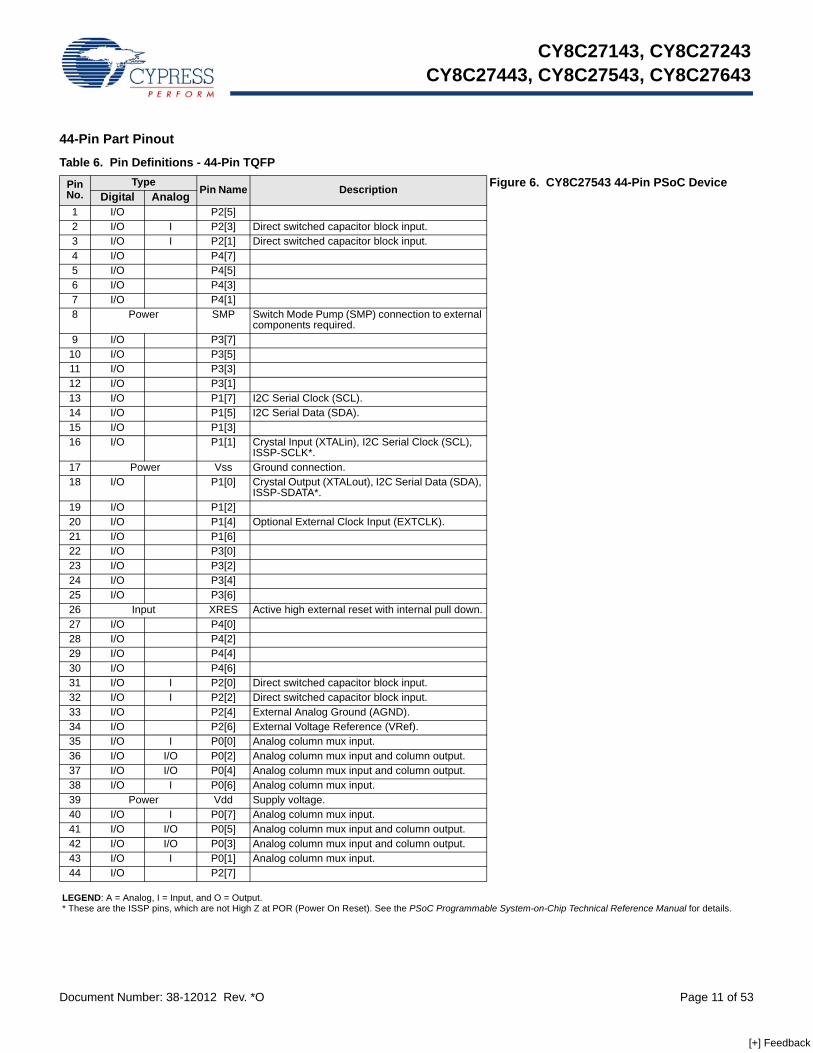
44-Pin Part Pinout
Table 6. Pin Definitions - 44-Pin TQFP
Pin No.
TypePin Name Description Figure 6. CY8C27543 44-Pin PSoC Device
Digital Analog1 I/O P2[5] 2 I/O I P2[3] Direct switched capacitor block input.3 I/O I P2[1] Direct switched capacitor block input.4 I/O P4[7]5 I/O P4[5]6 I/O P4[3]7 I/O P4[1]8 Power SMP Switch Mode Pump (SMP) connection to external
components required.9 I/O P3[7]
10 I/O P3[5]11 I/O P3[3]12 I/O P3[1]13 I/O P1[7] I2C Serial Clock (SCL).14 I/O P1[5] I2C Serial Data (SDA).15 I/O P1[3]16 I/O P1[1] Crystal Input (XTALin), I2C Serial Clock (SCL),
ISSP-SCLK*.17 Power Vss Ground connection.18 I/O P1[0] Crystal Output (XTALout), I2C Serial Data (SDA),
ISSP-SDATA*.19 I/O P1[2]20 I/O P1[4] Optional External Clock Input (EXTCLK).21 I/O P1[6]22 I/O P3[0]23 I/O P3[2]24 I/O P3[4]25 I/O P3[6]26 Input XRES Active high external reset with internal pull down.27 I/O P4[0]28 I/O P4[2]29 I/O P4[4]30 I/O P4[6]31 I/O I P2[0] Direct switched capacitor block input.32 I/O I P2[2] Direct switched capacitor block input.33 I/O P2[4] External Analog Ground (AGND).34 I/O P2[6] External Voltage Reference (VRef).35 I/O I P0[0] Analog column mux input.36 I/O I/O P0[2] Analog column mux input and column output.37 I/O I/O P0[4] Analog column mux input and column output.38 I/O I P0[6] Analog column mux input.39 Power Vdd Supply voltage.40 I/O I P0[7] Analog column mux input.41 I/O I/O P0[5] Analog column mux input and column output.42 I/O I/O P0[3] Analog column mux input and column output.43 I/O I P0[1] Analog column mux input.44 I/O P2[7]
LEGEND: A = Analog, I = Input, and O = Output.* These are the ISSP pins, which are not High Z at POR (Power On Reset). See the PSoC Programmable System-on-Chip Technical Reference Manual for details.
[+] Feedback

CY8C27143, CY8C27243CY8C27443, CY8C27543, CY8C27643
Document Number: 38-12012 Rev. *O Page 12 of 53
48-Pin Part PinoutTable 7. 48-Pin Part Pinout (SSOP)
Pin No.
Type Pin Name Description Figure 7. CY8C27643 48-Pin PSoC Device
Digital Analog1 I/O I P0[7] Analog column mux input.2 I/O I/O P0[5] Analog column mux input and column output.3 I/O I/O P0[3] Analog column mux input and column output.4 I/O I P0[1] Analog column mux input.5 I/O P2[7]6 I/O P2[5]7 I/O I P2[3] Direct switched capacitor block input.8 I/O I P2[1] Direct switched capacitor block input.9 I/O P4[7]10 I/O P4[5]11 I/O P4[3]12 I/O P4[1]13 Power SMP Switch Mode Pump (SMP) connection to
external components required.14 I/O P3[7]15 I/O P3[5]16 I/O P3[3]17 I/O P3[1]18 I/O P5[3]19 I/O P5[1]20 I/O P1[7] I2C Serial Clock (SCL).21 I/O P1[5] I2C Serial Data (SDA).22 I/O P1[3]23 I/O P1[1] Crystal Input (XTALin), I2C Serial Clock
(SCL), ISSP-SCLK*.24 Power Vss Ground connection.25 I/O P1[0] Crystal Output (XTALout), I2C Serial Data
(SDA), ISSP-SDATA.*26 I/O P1[2]27 I/O P1[4] Optional External Clock Input (EXTCLK).28 I/O P1[6]29 I/O P5[0]30 I/O P5[2]31 I/O P3[0]32 I/O P3[2]33 I/O P3[4]34 I/O P3[6]35 Input XRES Active high external reset with internal pull
down.36 I/O P4[0]37 I/O P4[2]38 I/O P4[4]39 I/O P4[6]40 I/O I P2[0] Direct switched capacitor block input.41 I/O I P2[2] Direct switched capacitor block input.42 I/O P2[4] External Analog Ground (AGND).43 I/O P2[6] External Voltage Reference (VRef).44 I/O I P0[0] Analog column mux input.45 I/O I/O P0[2] Analog column mux input and column output.46 I/O I/O P0[4] Analog column mux input and column output.47 I/O I P0[6] Analog column mux input.48 Power Vdd Supply voltage.
LEGEND: A = Analog, I = Input, and O = Output.* These are the ISSP pins, which are not High Z at POR (Power On Reset). See the PSoC Mixed-Signal Array Technical Reference Manual for details.
SSOP
A, I, P0[7] VddA, IO, P0[5] P0[6], A, IA, IO, P0[3] P0[4], A, IO
A, I, P0[1] P0[2], A, IOP2[7] P0[0], A, IP2[5] P2[6], External VRef
A, I, P2[3] P2[4], External AGNDA, I, P2[1] P2[2], A, I
P4[7] P2[0], A, IP4[5] P4[6]P4[3] P4[4]P4[1] P4[2]SMP P4[0]
P3[7] XRESP3[5] P3[6]P3[3] P3[4]P3[1] P3[2]P5[3] P3[0]P5[1] P5[2]
I2C SCL, P1[7] P5[0]I2C SDA, P1[5] P1[6]
P1[3] P1[4], EXTCLKI2C SCL, XTALin, P1[1] P1[2]
Vss P1[0], XTALout, I2C SDA
123456789
101112131415161718192021222324
48474645
4344
42
4041
3938373635
3334
3231302928272625
[+] Feedback

CY8C27143, CY8C27243CY8C27443, CY8C27543, CY8C27643
Document Number: 38-12012 Rev. *O Page 13 of 53
Table 8. 48-Pin Part Pinout (QFN)*
Pin No.
Type Pin Name Description Figure 8. CY8C27643 48-Pin PSoC Device
Digital Analog1 I/O I P2[3] Direct switched capacitor block input.2 I/O I P2[1] Direct switched capacitor block input.3 I/O P4[7]4 I/O P4[5]5 I/O P4[3]6 I/O P4[1]7 Power SMP Switch Mode Pump (SMP) connection to
external components required.8 I/O P3[7]9 I/O P3[5]10 I/O P3[3]11 I/O P3[1]12 I/O P5[3]13 I/O P5[1]14 I/O P1[7] I2C Serial Clock (SCL).15 I/O P1[5] I2C Serial Data (SDA).16 I/O P1[3]17 I/O P1[1] Crystal Input (XTALin), I2C Serial Clock (SCL),
ISSP-SCLK**.18 Power Vss Ground connection.19 I/O P1[0] Crystal Output (XTALout), I2C Serial Data
(SDA), ISSP-SDATA**.20 I/O P1[2]21 I/O P1[4] Optional External Clock Input (EXTCLK).22 I/O P1[6]23 I/O P5[0]24 I/O P5[2]25 I/O P3[0]26 I/O P3[2]27 I/O P3[4]28 I/O P3[6]29 Input XRES Active high external reset with internal pull
down.30 I/O P4[0]31 I/O P4[2]32 I/O P4[4]33 I/O P4[6]34 I/O I P2[0] Direct switched capacitor block input.35 I/O I P2[2] Direct switched capacitor block input.36 I/O P2[4] External Analog Ground (AGND).37 I/O P2[6] External Voltage Reference (VRef).38 I/O I P0[0] Analog column mux input.39 I/O I/O P0[2] Analog column mux input and column output.40 I/O I/O P0[4] Analog column mux input and column output.41 I/O I P0[6] Analog column mux input.42 Power Vdd Supply voltage.43 I/O I P0[7] Analog column mux input.44 I/O I/O P0[5] Analog column mux input and column output.45 I/O I/O P0[3] Analog column mux input and column output.46 I/O I P0[1] Analog column mux input.47 I/O P2[7]48 I/O P2[5]
LEGEND: A = Analog, I = Input, and O = Output.* The QFN package has a center pad that must be connected to ground (Vss). ** These are the ISSP pins, which are not High Z at POR (Power On Reset). See the PSoC Mixed-Signal Array Technical Reference Manual for details.
QFN(Top View )
P2[5]
P2[7]
P0[1]
, A, I
P0[3]
, A, IO
P0[5]
, A, IO
P0[7]
, A, I
Vdd
P0[6]
, A, I
P0[4]
, A, IO
P0[2]
, A, IO
P0[0]
, A, I
P2[6]
, Exte
rnal
VRef
101112
A, I, P2[3]A, I, P2[1]
P4[7]P4[5]P4[3]P4[1]SMP
P3[7]P3[5]P3[3]P3[1]P5[3]
3534333231302928272625
3648 47 46 45 44 43 42 41 40 39 38 37
P2[2], A, IP2[0], A, IP4[6]P4[4]P4[2]P4[0]XRESP3[6]P3[4]P3[2]P3[0]
P2[4], External AGND123456789
13 14 15 16 17 18 19 20 21 22 23 24
P5[1]
I2C SC
L, P1[7
]I2
C SDA
, P1[
5]P1
[3] I2
C SCL
, XTA
Lin, P
1[1] Vss
I2C SD
A, XT
ALou
t, P1[
0]P1
[2]EX
TCLK
, P1[4
]P1
[6]P5
[0]P5
[2]
[+] Feedback

CY8C27143, CY8C27243CY8C27443, CY8C27543, CY8C27643
Document Number: 38-12012 Rev. *O Page 14 of 53
56-Pin Part PinoutThe 56-pin SSOP part is for the CY8C27002 On-Chip Debug (OCD) PSoC device.Note This part is only used for in-circuit debugging. It is NOT available for production.
Table 9. 56-Pin Part Pinout (SSOP)
Pin No.
Type Pin Name Description Figure 9. CY8C27002 56-Pin PSoC Device
Digital Analog1 NC No connection.2 I/O I P0[7] Analog column mux input.3 I/O I P0[5] Analog column mux input and column
output.4 I/O I P0[3] Analog column mux input and column
output.5 I/O I P0[1] Analog column mux input.6 I/O P2[7]7 I/O P2[5]8 I/O I P2[3] Direct switched capacitor block input.9 I/O I P2[1] Direct switched capacitor block input.10 I/O P4[7]11 I/O P4[5]12 I/O I P4[3]13 I/O I P4[1]14 OCD OCDE OCD even data I/O.15 OCD OCDO OCD odd data output.16 Power SMP Switch Mode Pump (SMP) connection to
required external components.17 I/O P3[7]18 I/O P3[5]19 I/O P3[3]20 I/O P3[1]21 I/O P5[3] Not for Production22 I/O P5[1]23 I/O P1[7] I2C Serial Clock (SCL).24 I/O P1[5] I2C Serial Data (SDA).25 NC No connection.26 I/O P1[3]27 I/O P1[1] Crystal Input (XTALin), I2C Serial Clock
(SCL), ISSP-SCLK*.28 Power Vdd Supply voltage.29 NC No connection.30 NC No connection..31 I/O P1[0] Crystal Output (XTALout), I2C Serial
Data (SDA), ISSP-SDATA*.32 I/O P1[2]33 I/O P1[4] Optional External Clock Input (EXTCLK).34 I/O P1[6]35 I/O P5[0]36 I/O P5[2]37 I/O P3[0]38 I/O P3[2]39 I/O P3[4]40 I/O P3[6]41 Input XRES Active high external reset with internal
pull down.
SSOP
1 562 553 544 535 526 517 508 499 48
10 4711 4612 4513 4414 4315 4216 4117 4018 3919 3820 3721 3622 3523 3424 3325 3226 3127 3028 29
VddP0[6], AIP0[4], AIOP0[2], AIOP0[0], AIP2[6], External VRefP2[4], External AGNDP2[2], AIP2[0], AIP4[6]P4[4]P4[2]P4[0]CCLKHCLKXRESP3[6]P3[4]P3[2]P3[0]P5[2]P5[0]P1[6]P1[4], EXTCLKP1[2]P1[0], XTALOut, I2C SDA, SDATANCNC
AI, P0[7]AIO, P0[5]AIO, P0[3]
AI, P0[1]P2[7]P2[5]
AI, P2[3]AI, P2[1]
P4[7]P4[5]P4[3]P4[1]
OCDEOCDO
SMPP3[7]P3[5]P3[3]P3[1]P5[3]P5[1]
I2C SCL, P1[7]I2C SDA, P1[5]
NCP1[3]
SCLK, I2C SCL, XTALIn, P1[1]Vss
NC
[+] Feedback

CY8C27143, CY8C27243CY8C27443, CY8C27543, CY8C27643
Document Number: 38-12012 Rev. *O Page 15 of 53
42 OCD HCLK OCD high-speed clock output.43 OCD CCLK OCD CPU clock output.44 I/O P4[0]45 I/O P4[2]46 I/O P4[4]47 I/O P4[6]48 I/O I P2[0] Direct switched capacitor block input.49 I/O I P2[2] Direct switched capacitor block input.50 I/O P2[4] External Analog Ground (AGND).51 I/O P2[6] External Voltage Reference (VRef).52 I/O I P0[0] Analog column mux input.53 I/O I P0[2] Analog column mux input and column
output.54 I/O I P0[4] Analog column mux input and column
output.55 I/O I P0[6] Analog column mux input.56 Power Vdd Supply voltage.
LEGEND: A = Analog, I = Input, O = Output, and OCD = On-Chip Debug.* These are the ISSP pins, which are not High Z at POR (Power On Reset). See the PSoC Mixed-Signal Array Technical Reference Manual for details.
Table 9. 56-Pin Part Pinout (SSOP)
[+] Feedback

CY8C27143, CY8C27243CY8C27443, CY8C27543, CY8C27643
Document Number: 38-12012 Rev. *O Page 16 of 53
Register ReferenceThis chapter lists the registers of the CY8C27x43 PSoC device.For detailed register information, reference the PSoC Programmable System-on-Chip Technical ReferenceManual.
Register ConventionsThe register conventions specific to this section are listed in thefollowing table.
Register Mapping TablesThe PSoC device has a total register address space of 512bytes. The register space is referred to as I/O space and isdivided into two banks. The XOI bit in the Flag register (CPU_F)determines which bank the user is currently in. When the XOI bitis set the user is in Bank 1.Note In the following register mapping tables, blank fields arereserved and must not be accessed.
Table 10. Register Conventions
Convention DescriptionR Read register or bit(s)W Write register or bit(s)L Logical register or bit(s)C Clearable register or bit(s)# Access is bit specific
Table 11. Register Map Bank 0 Table: User Space
Nam
e
Addr
(0,Hex)
Access
Nam
e
Addr
(0,Hex)
Access
Nam
e
Addr
(0,Hex)
Access
Nam
e
Addr
(0,Hex)
Access
PRT0DR 00 RW 40 ASC10CR0 80 RW C0PRT0IE 01 RW 41 ASC10CR1 81 RW C1PRT0GS 02 RW 42 ASC10CR2 82 RW C2PRT0DM2 03 RW 43 ASC10CR3 83 RW C3PRT1DR 04 RW 44 ASD11CR0 84 RW C4PRT1IE 05 RW 45 ASD11CR1 85 RW C5PRT1GS 06 RW 46 ASD11CR2 86 RW C6PRT1DM2 07 RW 47 ASD11CR3 87 RW C7PRT2DR 08 RW 48 ASC12CR0 88 RW C8PRT2IE 09 RW 49 ASC12CR1 89 RW C9PRT2GS 0A RW 4A ASC12CR2 8A RW CAPRT2DM2 0B RW 4B ASC12CR3 8B RW CBPRT3DR 0C RW 4C ASD13CR0 8C RW CCPRT3IE 0D RW 4D ASD13CR1 8D RW CDPRT3GS 0E RW 4E ASD13CR2 8E RW CEPRT3DM2 0F RW 4F ASD13CR3 8F RW CFPRT4DR 10 RW 50 ASD20CR0 90 RW D0PRT4IE 11 RW 51 ASD20CR1 91 RW D1PRT4GS 12 RW 52 ASD20CR2 92 RW D2PRT4DM2 13 RW 53 ASD20CR3 93 RW D3PRT5DR 14 RW 54 ASC21CR0 94 RW D4PRT5IE 15 RW 55 ASC21CR1 95 RW D5PRT5GS 16 RW 56 ASC21CR2 96 RW I2C_CFG D6 RWPRT5DM2 17 RW 57 ASC21CR3 97 RW I2C_SCR D7 #
18 58 ASD22CR0 98 RW I2C_DR D8 RW19 59 ASD22CR1 99 RW I2C_MSCR D9 #1A 5A ASD22CR2 9A RW INT_CLR0 DA RW1B 5B ASD22CR3 9B RW INT_CLR1 DB RW1C 5C ASC23CR0 9C RW DC1D 5D ASC23CR1 9D RW INT_CLR3 DD RW1E 5E ASC23CR2 9E RW INT_MSK3 DE RW1F 5F ASC23CR3 9F RW DF
DBB00DR0 20 # AMX_IN 60 RW A0 INT_MSK0 E0 RWDBB00DR1 21 W 61 A1 INT_MSK1 E1 RWDBB00DR2 22 RW 62 A2 INT_VC E2 RCDBB00CR0 23 # ARF_CR 63 RW A3 RES_WDT E3 WDBB01DR0 24 # CMP_CR0 64 # A4 DEC_DH E4 RCDBB01DR1 25 W ASY_CR 65 # A5 DEC_DL E5 RCBlank fields are Reserved and must not be accessed. # Access is bit specific.
[+] Feedback

CY8C27143, CY8C27243CY8C27443, CY8C27543, CY8C27643
Document Number: 38-12012 Rev. *O Page 17 of 53
DBB01DR2 26 RW CMP_CR1 66 RW A6 DEC_CR0 E6 RWDBB01CR0 27 # 67 A7 DEC_CR1 E7 RWDCB02DR0 28 # 68 A8 MUL_X E8 WDCB02DR1 29 W 69 A9 MUL_Y E9 WDCB02DR2 2A RW 6A AA MUL_DH EA RDCB02CR0 2B # 6B AB MUL_DL EB RDCB03DR0 2C # 6C AC ACC_DR1 EC RWDCB03DR1 2D W 6D AD ACC_DR0 ED RWDCB03DR2 2E RW 6E AE ACC_DR3 EE RWDCB03CR0 2F # 6F AF ACC_DR2 EF RWDBB10DR0 30 # ACB00CR3 70 RW RDI0RI B0 RW F0DBB10DR1 31 W ACB00CR0 71 RW RDI0SYN B1 RW F1DBB10DR2 32 RW ACB00CR1 72 RW RDI0IS B2 RW F2DBB10CR0 33 # ACB00CR2 73 RW RDI0LT0 B3 RW F3DBB11DR0 34 # ACB01CR3 74 RW RDI0LT1 B4 RW F4DBB11DR1 35 W ACB01CR0 75 RW RDI0RO0 B5 RW F5DBB11DR2 36 RW ACB01CR1 76 RW RDI0RO1 B6 RW F6DBB11CR0 37 # ACB01CR2 77 RW B7 CPU_F F7 RLDCB12DR0 38 # ACB02CR3 78 RW RDI1RI B8 RW F8DCB12DR1 39 W ACB02CR0 79 RW RDI1SYN B9 RW F9DCB12DR2 3A RW ACB02CR1 7A RW RDI1IS BA RW FADCB12CR0 3B # ACB02CR2 7B RW RDI1LT0 BB RW FBDCB13DR0 3C # ACB03CR3 7C RW RDI1LT1 BC RW FCDCB13DR1 3D W ACB03CR0 7D RW RDI1RO0 BD RW FDDCB13DR2 3E RW ACB03CR1 7E RW RDI1RO1 BE RW CPU_SCR1 FE #DCB13CR0 3F # ACB03CR2 7F RW BF CPU_SCR0 FF #
Table 11. Register Map Bank 0 Table: User Space (continued)
Nam
e
Addr
(0,Hex)
Access
Nam
e
Addr
(0,Hex)
Access
Nam
e
Addr
(0,Hex)
Access
Nam
e
Addr
(0,Hex)
Access
Blank fields are Reserved and must not be accessed. # Access is bit specific.
Table 12. Register Map Bank 1 Table: Configuration Space
Nam
e
Addr
(1,Hex)
Access
Nam
e
Addr
(1,Hex)
Access
Nam
e
Addr
(1,Hex)
Access
Nam
e
Addr
(1,Hex)
Access
PRT0DM0 00 RW 40 ASC10CR0 80 RW C0PRT0DM1 01 RW 41 ASC10CR1 81 RW C1PRT0IC0 02 RW 42 ASC10CR2 82 RW C2PRT0IC1 03 RW 43 ASC10CR3 83 RW C3PRT1DM0 04 RW 44 ASD11CR0 84 RW C4PRT1DM1 05 RW 45 ASD11CR1 85 RW C5PRT1IC0 06 RW 46 ASD11CR2 86 RW C6PRT1IC1 07 RW 47 ASD11CR3 87 RW C7PRT2DM0 08 RW 48 ASC12CR0 88 RW C8PRT2DM1 09 RW 49 ASC12CR1 89 RW C9PRT2IC0 0A RW 4A ASC12CR2 8A RW CAPRT2IC1 0B RW 4B ASC12CR3 8B RW CBPRT3DM0 0C RW 4C ASD13CR0 8C RW CCPRT3DM1 0D RW 4D ASD13CR1 8D RW CDPRT3IC0 0E RW 4E ASD13CR2 8E RW CEPRT3IC1 0F RW 4F ASD13CR3 8F RW CFPRT4DM0 10 RW 50 ASD20CR0 90 RW GDI_O_IN D0 RWPRT4DM1 11 RW 51 ASD20CR1 91 RW GDI_E_IN D1 RWPRT4IC0 12 RW 52 ASD20CR2 92 RW GDI_O_OU D2 RWPRT4IC1 13 RW 53 ASD20CR3 93 RW GDI_E_OU D3 RWPRT5DM0 14 RW 54 ASC21CR0 94 RW D4PRT5DM1 15 RW 55 ASC21CR1 95 RW D5PRT5IC0 16 RW 56 ASC21CR2 96 RW D6PRT5IC1 17 RW 57 ASC21CR3 97 RW D7
18 58 ASD22CR0 98 RW D819 59 ASD22CR1 99 RW D91A 5A ASD22CR2 9A RW DA1B 5B ASD22CR3 9B RW DB
Blank fields are Reserved and must not be accessed. # Access is bit specific.
[+] Feedback

CY8C27143, CY8C27243CY8C27443, CY8C27543, CY8C27643
Document Number: 38-12012 Rev. *O Page 18 of 53
1C 5C ASC23CR0 9C RW DC1D 5D ASC23CR1 9D RW OSC_GO_EN DD RW1E 5E ASC23CR2 9E RW OSC_CR4 DE RW1F 5F ASC23CR3 9F RW OSC_CR3 DF RW
DBB00FN 20 RW CLK_CR0 60 RW A0 OSC_CR0 E0 RWDBB00IN 21 RW CLK_CR1 61 RW A1 OSC_CR1 E1 RWDBB00OU 22 RW ABF_CR0 62 RW A2 OSC_CR2 E2 RW
23 AMD_CR0 63 RW A3 VLT_CR E3 RWDBB01FN 24 RW 64 A4 VLT_CMP E4 RDBB01IN 25 RW 65 A5 E5DBB01OU 26 RW AMD_CR1 66 RW A6 E6
27 ALT_CR0 67 RW A7 E7DCB02FN 28 RW ALT_CR1 68 RW A8 IMO_TR E8 WDCB02IN 29 RW CLK_CR2 69 RW A9 ILO_TR E9 WDCB02OU 2A RW 6A AA BDG_TR EA RW
2B 6B AB ECO_TR EB WDCB03FN 2C RW 6C AC ECDCB03IN 2D RW 6D AD EDDCB03OU 2E RW 6E AE EE
2F 6F AF EFDBB10FN 30 RW ACB00CR3 70 RW RDI0RI B0 RW F0DBB10IN 31 RW ACB00CR0 71 RW RDI0SYN B1 RW F1DBB10OU 32 RW ACB00CR1 72 RW RDI0IS B2 RW F2
33 ACB00CR2 73 RW RDI0LT0 B3 RW F3DBB11FN 34 RW ACB01CR3 74 RW RDI0LT1 B4 RW F4DBB11IN 35 RW ACB01CR0 75 RW RDI0RO0 B5 RW F5DBB11OU 36 RW ACB01CR1 76 RW RDI0RO1 B6 RW F6
37 ACB01CR2 77 RW B7 CPU_F F7 RLDCB12FN 38 RW ACB02CR3 78 RW RDI1RI B8 RW F8DCB12IN 39 RW ACB02CR0 79 RW RDI1SYN B9 RW F9DCB12OU 3A RW ACB02CR1 7A RW RDI1IS BA RW FA
3B ACB02CR2 7B RW RDI1LT0 BB RW FBDCB13FN 3C RW ACB03CR3 7C RW RDI1LT1 BC RW FCDCB13IN 3D RW ACB03CR0 7D RW RDI1RO0 BD RW FDDCB13OU 3E RW ACB03CR1 7E RW RDI1RO1 BE RW CPU_SCR1 FE #
3F ACB03CR2 7F RW BF CPU_SCR0 FF #
Table 12. Register Map Bank 1 Table: Configuration Space (continued)
Nam
e
Addr
(1,Hex)
Access
Nam
e
Addr
(1,Hex)
Access
Nam
e
Addr
(1,Hex)
Access
Nam
e
Addr
(1,Hex)
Access
Blank fields are Reserved and must not be accessed. # Access is bit specific.
[+] Feedback

CY8C27143, CY8C27243CY8C27443, CY8C27543, CY8C27643
Document Number: 38-12012 Rev. *O Page 19 of 53
Electrical SpecificationsThis chapter presents the DC and AC electrical specifications of the CY8C27x43 PSoC device. For the most up to date electricalspecifications, confirm that you have the most recent data sheet by going to the web at http://www.cypress.com/psoc.Specifications are valid for -40°C ≤ TA ≤ 85°C and TJ ≤ 100°C, except where noted. Specifications for devices running at greater than12 MHz are valid for -40°C ≤ TA ≤ 70°C and TJ ≤ 82°C.
Figure 10. Voltage versus CPU Frequency
The following table lists the units of measure that are used in this chapter.
Table 13. Units of Measure
Symbol Unit of Measure Symbol Unit of MeasureoC degree Celsius μW microwattsdB decibels mA milli-amperefF femto farad ms milli-secondHz hertz mV milli-voltsKB 1024 bytes nA nanoampereKbit 1024 bits ns nanosecondkHz kilohertz nV nanovoltskΩ kilohm W ohm
MHz megahertz pA picoampereMΩ megaohm pF picofaradμA microampere pp peak-to-peakμF microfarad ppm parts per millionμH microhenry ps picosecondμs microsecond sps samples per secondμV microvolts s sigma: one standard deviation
μVrms microvolts root-mean-square V volts
5.25
4.75
3.00
93 kHz 12 MHz 24 MHzCPU Frequency
Vdd Voltage
Valid
Operating
Region
[+] Feedback

CY8C27143, CY8C27243CY8C27443, CY8C27543, CY8C27643
Document Number: 38-12012 Rev. *O Page 20 of 53
Absolute Maximum RatingsExceeding maximum ratings may shorten the useful life of the device. User guidelines are not tested.
Operating Temperature
Table 14. Absolute Maximum Ratings
Symbol Description Min Typ Max Unit NotesTSTG Storage Temperature -55 25 +100 oC Higher storage temperatures reduce
data retention time. Recommended storage temperature is +25°C ± 25°C. Extended duration storage temperatures above 65oC degrade reliability.
TA Ambient Temperature with Power Applied -40 – +85 oCVdd Supply Voltage on Vdd Relative to Vss -0.5 – +6.0 VVIO DC Input Voltage Vss- 0.5 – Vdd + 0.5 VVIOZ DC Voltage Applied to Tri-state Vss -
0.5– Vdd + 0.5 V
IMIO Maximum Current into any Port Pin -25 – +50 mAIMAIO Maximum Current into any Port Pin Configured
as Analog Driver-50 – +50 mA
ESD Electro Static Discharge Voltage 2000 – – V Human Body Model ESD.LU Latch up Current – – 200 mA
Table 15. Operating Temperature
Symbol Description Min Typ Max Unit NotesTA Ambient Temperature -40 – +85 oCTJ Junction Temperature -40 – +100 oC The temperature rise from ambient
to junction is package specific. See “Thermal Impedances” on page 46. The user must limit the power consumption to comply with this requirement.
[+] Feedback

CY8C27143, CY8C27243CY8C27443, CY8C27543, CY8C27643
Document Number: 38-12012 Rev. *O Page 21 of 53
DC Electrical Characteristics
DC Chip-Level SpecificationsThe following table lists guaranteed maximum and minimum specifications for the voltage and temperature ranges: 4.75V to 5.25Vand -40°C ≤ TA ≤ 85°C, or 3.0V to 3.6V and -40°C ≤ TA ≤ 85°C, respectively. Typical parameters apply to 5V and 3.3V at 25°C andare for design guidance only.
DC General Purpose I/O SpecificationsThe following table lists guaranteed maximum and minimum specifications for the voltage and temperature ranges: 4.75V to 5.25Vand -40°C ≤ TA ≤ 85°C, or 3.0V to 3.6V and -40°C ≤ TA ≤ 85°C, respectively. Typical parameters apply to 5V and 3.3V at 25°C andare for design guidance only.
Table 16. DC Chip-Level Specifications
Symbol Description Min Typ Max Unit NotesVdd Supply Voltage 3.00 – 5.25 VIDD Supply Current – 5 8 mA Conditions are Vdd = 5.0V, TA = 25 oC,
CPU = 3 MHz, SYSCLK doubler disabled. VC1 = 1.5 MHz, VC2 = 93.75 kHz, VC3 = 93.75 kHz.
IDD3 Supply Current – 3.3 6.0 mA Conditions are Vdd = 3.3V, TA = 25 oC, CPU = 3 MHz, SYSCLK doubler disabled. VC1 = 1.5 MHz, VC2 = 93.75 kHz, VC3 = 93.75 kHz.
ISB Sleep (Mode) Current with POR, LVD, Sleep Timer, and WDT.[3]
– 3 6.5 μA Conditions are with internal slow speed oscillator, Vdd = 3.3V, -40 oC ≤ TA ≤ 55 oC.
ISBH Sleep (Mode) Current with POR, LVD, Sleep Timer, and WDT at high temperature.[3]
– 4 25 μA Conditions are with internal slow speed oscillator, Vdd = 3.3V, 55 oC < TA ≤ 85 oC.
ISBXTL Sleep (Mode) Current with POR, LVD, Sleep Timer, WDT, and external crystal.[3]
– 4 7.5 μA Conditions are with properly loaded, 1 μW max, 32.768 kHz crystal. Vdd = 3.3V, -40 oC ≤ TA ≤ 55 oC.
ISBXTLH Sleep (Mode) Current with POR, LVD, Sleep Timer, WDT, and external crystal at high temperature.[3]
– 5 26 μA Conditions are with properly loaded, 1 μW max, 32.768 kHz crystal. Vdd = 3.3V, 55 oC < TA ≤ 85 oC.
VREF Reference Voltage (Bandgap) for Silicon A [4] 1.275 1.300 1.325 V Trimmed for appropriate Vdd.VREF Reference Voltage (Bandgap) for Silicon B [4] 1.280 1.300 1.320 V Trimmed for appropriate Vdd.
Notes3. Standby current includes all functions (POR, LVD, WDT, Sleep Time) needed for reliable system operation. This must be compared with devices that have similar
functions enabled.4. Refer to the “Ordering Information” on page 50.
Table 17. DC GPIO SpecificationsSymbol Description Min Typ Max Unit NotesRPU Pull up Resistor 4 5.6 8 kΩRPD Pull down Resistor 4 5.6 8 kΩVOH High Output Level Vdd -
1.0– – V IOH = 10 mA, Vdd = 4.75 to 5.25V
(8 total loads, 4 on even port pins (for example, P0[2], P1[4]), 4 on odd port pins (for example, P0[3], P1[5])).
VOL Low Output Level – – 0.75 V IOL = 25 mA, Vdd = 4.75 to 5.25V (8 total loads, 4 on even port pins (for example, P0[2], P1[4]), 4 on odd port pins (for example, P0[3], P1[5])).
[+] Feedback

CY8C27143, CY8C27243CY8C27443, CY8C27543, CY8C27643
Document Number: 38-12012 Rev. *O Page 22 of 53
DC Operational Amplifier SpecificationsThe following tables list guaranteed maximum and minimum specifications for the voltage and temperature ranges: 4.75V to 5.25Vand -40°C ≤ TA ≤ 85°C, or 3.0V to 3.6V and -40°C ≤ TA ≤ 85°C, respectively. Typical parameters apply to 5V and 3.3V at 25°C andare for design guidance only.The Operational Amplifier is a component of both the Analog Continuous Time PSoC blocks and the Analog Switched Cap PSoCblocks. The guaranteed specifications are measured in the Analog Continuous Time PSoC block. Typical parameters apply to 5V at25°C and are for design guidance only.
IOH High Level Source Current 10 – – mA VOH = Vdd-1.0V, see the limitations of the total current in the note for VOH
IOL Low Level Sink Current 25 – – mA VOL = 0.75V, see the limitations of the total current in the note for VOL
VIL Input Low Level – – 0.8 V Vdd = 3.0 to 5.25VIH Input High Level 2.1 – V Vdd = 3.0 to 5.25VH Input Hysterisis – 60 – mVIIL Input Leakage (Absolute Value) – 1 – nA Gross tested to 1 μA.CIN Capacitive Load on Pins as Input – 3.5 10 pF Package and pin dependent.
Temp = 25oC.COUT Capacitive Load on Pins as Output – 3.5 10 pF Package and pin dependent.
Temp = 25oC.
Table 17. DC GPIO Specifications (continued)
Symbol Description Min Typ Max Unit Notes
Table 18. 5V DC Operational Amplifier SpecificationsSymbol Description Min Typ Max Unit Notes
VOSOA Input Offset Voltage (absolute value) Power = Low, Opamp Bias = HighPower = Medium, Opamp Bias = HighPower = High, Opamp Bias = High
– 1.6 1.3 1.2
10 8
7.5
mV mV mV
––
TCVOSOA Average Input Offset Voltage Drift – 7.0 35.0 μV/oCIEBOA Input Leakage Current (Port 0 Analog Pins) – 20 – pA Gross tested to 1 μA.CINOA Input Capacitance (Port 0 Analog Pins) – 4.5 9.5 pF Package and pin dependent.
Temp = 25oC. VCMOA Common Mode Voltage Range
Common Mode Voltage Range (high power or high opamp bias)
0.0 – VddVdd - 0.5
VV
The common-mode input voltage range is measured through an analog output buffer. The specification includes the limitations imposed by the characteristics of the analog output buffer.
0.5 –
CMRROA Common Mode Rejection RatioPower = LowPower = MediumPower = High
606060
– – dB Specification is applicable at high power. For all other bias modes (except high power, high opamp bias), minimum is 60 dB.
GOLOA Open Loop GainPower = LowPower = MediumPower = High
606080
– – dB Specification is applicable at high power. For all other bias modes (except high power, high opamp bias), minimum is 60 dB.
VOHIGHOA High Output Voltage Swing (internal signals)Power = LowPower = MediumPower = High
Vdd - 0.2Vdd - 0.2Vdd - 0.5
–––
–––
VVV
[+] Feedback

CY8C27143, CY8C27243CY8C27443, CY8C27543, CY8C27643
Document Number: 38-12012 Rev. *O Page 23 of 53
VOLOWOA Low Output Voltage Swing (internal signals)Power = LowPower = MediumPower = High
–––
–––
0.20.20.5
VVV
ISOA Supply Current (including associated AGND buffer)Power = Low, Opamp Bias = LowPower = Low, Opamp Bias = HighPower = Medium, Opamp Bias = LowPower = Medium, Opamp Bias = HighPower = High, Opamp Bias = LowPower = High, Opamp Bias = High
––––––
150300600
120024004600
200400800
160032006400
μAμAμAμAμAμA
PSRROA Supply Voltage Rejection Ratio 60 – – dB Vss ≤ VIN ≤ (Vdd - 2.25) or (Vdd - 1.25V) ≤ VIN ≤ Vdd.
Table 18. 5V DC Operational Amplifier Specifications (continued)
Symbol Description Min Typ Max Unit Notes
Table 19. 3.3V DC Operational Amplifier Specifications
Symbol Description Min Typ Max Unit NotesVOSOA Input Offset Voltage (absolute value)
Power = Low, Opamp Bias = HighPower = Medium, Opamp Bias = HighHigh Power is 5 Volts Only
––
1.65 1.32
10 8
mV mV
TCVOSOA Average Input Offset Voltage Drift – 7.0 35.0 μV/oCIEBOA Input Leakage Current (Port 0 Analog Pins) – 20 – pA Gross tested to 1 μA.CINOA Input Capacitance (Port 0 Analog Pins) – 4.5 9.5 pF Package and pin dependent.
Temp = 25oC.VCMOA Common Mode Voltage Range 0.2 – Vdd - 0.2 V The common-mode input
voltage range is measured through an analog output buffer. The specification includes the limitations imposed by the characteristics of the analog output buffer.
CMRROA Common Mode Rejection RatioPower = LowPower = MediumPower = High
505050
–––
–––
dBdBdB
Specification is applicable at high power. For all other bias modes (except high power, high opamp bias), minimum is 60 dB.
GOLOA Open Loop GainPower = LowPower = MediumPower = High
606080
–––
–––
dBdBdB
Specification is applicable at high power. For all other bias modes (except high power, high opamp bias), minimum is 60 dB.
VOHIGHOA High Output Voltage Swing (internal signals)Power = LowPower = MediumPower = High is 5V only
Vdd - 0.2Vdd - 0.2Vdd - 0.2
–––
–––
VVV
[+] Feedback

CY8C27143, CY8C27243CY8C27443, CY8C27543, CY8C27643
Document Number: 38-12012 Rev. *O Page 24 of 53
DC Low Power Comparator SpecificationsThe following table lists guaranteed maximum and minimum specifications for the voltage and temperature ranges: 4.75V to 5.25Vand -40°C ≤ TA ≤ 85°C, 3.0V to 3.6V and -40°C ≤ TA ≤ 85°C, or 2.4V to 3.0V and -40°C ≤ TA ≤ 85°C, respectively. Typical parametersapply to 5V at 25°C and are for design guidance only.
DC Analog Output Buffer SpecificationsThe following tables list guaranteed maximum and minimum specifications for the voltage and temperature ranges: 4.75V to 5.25Vand -40°C ≤ TA ≤ 85°C, or 3.0V to 3.6V and -40°C ≤ TA ≤ 85°C, respectively. Typical parameters apply to 5V and 3.3V at 25°C andare for design guidance only.
VOLOWOA Low Output Voltage Swing (internal signals)Power = LowPower = MediumPower = High
–––
–––
0.20.20.2
VVV
ISOA Supply Current (including associated AGND buffer)Power = Low, Opamp Bias = LowPower = Low, Opamp Bias = HighPower = Medium, Opamp Bias = LowPower = Medium, Opamp Bias = HighPower = High, Opamp Bias = LowPower = High, Opamp Bias = High
––––––
150300600
120024004600
200400800
160032006400
μAμAμAμAμAμA
PSRROA Supply Voltage Rejection Ratio 50 80 – dB Vss ≤ VIN ≤ (Vdd - 2.25) or (Vdd - 1.25V) ≤ VIN ≤ Vdd.
Table 19. 3.3V DC Operational Amplifier Specifications (continued)
Symbol Description Min Typ Max Unit Notes
Table 20. DC Low Power Comparator SpecificationsSymbol Description Min Typ Max Unit
VREFLPC Low power comparator (LPC) reference voltage range
0.2 – Vdd - 1 V
ISLPC LPC supply current – 10 40 μAVOSLPC LPC voltage offset – 2.5 30 mV
Table 21. 5V DC Analog Output Buffer Specifications
Symbol Description Min Typ Max UnitVOSOB Input Offset Voltage (Absolute Value) – 3 12 mVTCVOSOB Average Input Offset Voltage Drift – +6 – μV/°CVCMOB Common-Mode Input Voltage Range 0.5 – Vdd - 1.0 VROUTOB Output Resistance
Power = LowPower = High
––
11
––
WW
VOHIGHOB High Output Voltage Swing (Load = 32 ohms to Vdd/2)Power = LowPower = High
0.5 x Vdd + 1.30.5 x Vdd + 1.3
––
––
VV
VOLOWOB Low Output Voltage Swing (Load = 32 ohms to Vdd/2)Power = LowPower = High
––
––
0.5 x Vdd - 1.30.5 x Vdd - 1.3
VV
ISOB Supply Current Including Bias Cell (No Load)Power = LowPower = High
––
1.12.6
5.18.8
mAmA
PSRROB Supply Voltage Rejection Ratio 60 64 – dBIOMAX Maximum Output Current – 40 – mA
[+] Feedback

CY8C27143, CY8C27243CY8C27443, CY8C27543, CY8C27643
Document Number: 38-12012 Rev. *O Page 25 of 53
DC Switch Mode Pump SpecificationsThe following table lists guaranteed maximum and minimum specifications for the voltage and temperature ranges: 4.75V to 5.25Vand -40°C ≤ TA ≤ 85°C, or 3.0V to 3.6V and -40°C ≤ TA ≤ 85°C, respectively. Typical parameters apply to 5V and 3.3V at 25°C andare for design guidance only.
Table 22. 3.3V DC Analog Output Buffer Specifications
Symbol Description Min Typ Max UnitsVOSOB Input Offset Voltage (Absolute Value) – 3 12 mVTCVOSOB Average Input Offset Voltage Drift – +6 – μV/°CVCMOB Common-Mode Input Voltage Range 0.5 - Vdd - 1.0 VROUTOB Output Resistance
Power = LowPower = High
––
11
––
WW
VOHIGHOB High Output Voltage Swing (Load = 1k ohms to Vdd/2)Power = LowPower = High
0.5 x Vdd + 1.00.5 x Vdd + 1.0
––
––
VV
VOLOWOB Low Output Voltage Swing (Load = 1k ohms to Vdd/2)Power = LowPower = High
––
––
0.5 x Vdd - 1.00.5 x Vdd - 1.0
VV
ISOB Supply Current Including Bias Cell (No Load)Power = LowPower = High –
0.82.0
2.04.3
mAmA
PSRROB Supply Voltage Rejection Ratio 60 64 – dB
Table 23. DC Switch Mode Pump (SMP) Specifications
Symbol Description Min Typ Max Unit NotesVPUMP 5V 5V Output Voltage 4.75 5.0 5.25 V Configuration of footnote.[5] Average,
neglecting ripple. SMP trip voltage is set to 5.0V.
VPUMP 3V 3V Output Voltage 3.00 3.25 3.60 V Configuration of footnote.[5] Average, neglecting ripple. SMP trip voltage is set to 3.25V.
IPUMP Available Output CurrentVBAT = 1.5V, VPUMP = 3.25VVBAT = 1.8V, VPUMP = 5.0V
85
––
––
mAmA
Configuration of footnote.[5]
SMP trip voltage is set to 3.25V. SMP trip voltage is set to 5.0V.
VBAT5V Input Voltage Range from Battery 1.8 – 5.0 V Configuration of footnote.[5] SMP trip voltage is set to 5.0V.
VBAT3V Input Voltage Range from Battery 1.0 – 3.3 V Configuration of footnote.[5] SMP trip voltage is set to 3.25V.
VBATSTART Minimum Input Voltage from Battery to Start Pump
1.1 – – V Configuration of footnote.[5]
ΔVPUMP_Line Line Regulation (over VBAT range) – 5 – %VO Configuration of footnote.[5] VO is the “Vdd Value for PUMP Trip” specified by the VM[2:0] setting in the DC POR and LVD Specification, Table 29 on page 30.
Note5. L1 = 2 mH inductor, C1 = 10 mF capacitor, D1 = Schottky diode. See Figure 11.
[+] Feedback

CY8C27143, CY8C27243CY8C27443, CY8C27543, CY8C27643
Document Number: 38-12012 Rev. *O Page 26 of 53
Figure 11. Basic Switch Mode Pump Circuit
DC Analog Reference SpecificationsThe following tables list guaranteed maximum and minimum specifications for the voltage and temperature ranges: 4.75V to 5.25Vand -40°C ≤ TA ≤ 85°C, or 3.0V to 3.6V and -40°C ≤ TA ≤ 85°C, respectively. Typical parameters apply to 5V and 3.3V at 25°C andare for design guidance only.The guaranteed specifications are measured through the Analog Continuous Time PSoC blocks. The power levels for AGND refer tothe power of the Analog Continuous Time PSoC block. The power levels for RefHi and RefLo refer to the Analog Reference Controlregister. The limits stated for AGND include the offset error of the AGND buffer local to the Analog Continuous Time PSoC block.Reference control power is high.Note Avoid using P2[4] for digital signaling when using an analog resource that depends on the Analog Reference. Some couplingof the digital signal may appear on the AGND.
ΔVPUMP_Load Load Regulation – 5 – %VO Configuration of footnote.[5] VO is the “Vdd Value for PUMP Trip” specified by the VM[2:0] setting in the DC POR and LVD Specification, Table 29 on page 30.
ΔVPUMP_Ripple Output Voltage Ripple (depends on capacitor/load)
– 100 – mVpp Configuration of footnote.[5] Load is 5 mA.
E3 Efficiency 35 50 – % Configuration of footnote.[5] Load is 5 mA. SMP trip voltage is set to 3.25V.
FPUMP Switching Frequency – 1.3 – MHzDCPUMP Switching Duty Cycle – 50 – %
Table 23. DC Switch Mode Pump (SMP) Specifications (continued)
Symbol Description Min Typ Max Unit Notes
Battery
C1
D1
+PSoCTM
Vdd
Vss
SMPVBAT
VPUMP
L1
Table 24. Silicon Revision A – 5V DC Analog Reference Specifications
Symbol Description Min Typ Max UnitBG Bandgap Voltage Reference 1.274 1.30 1.326 V– AGND = Vdd/2[6] Vdd/2 - 0.030 Vdd/2 - 0.004 Vdd/2 + 0.003 V– AGND = 2 x BandGap[6] 2 x BG - 0.043 2 x BG - 0.010 2 x BG + 0.024 V– AGND = P2[4] (P2[4] = Vdd/2)[6] P2[4] - 0.013 P2[4] P2[4] + 0.014 V– AGND = BandGap[6] BG - 0.009 BG BG + 0.009 V– AGND = 1.6 x BandGap[6] 1.6 x BG - 0.018 1.6 x BG 1.6 x BG + 0.018 V– AGND Block to Block Variation
(AGND = Vdd/2)[6]-0.034 0.000 0.034 V
– RefHi = Vdd/2 + BandGap Vdd/2 + BG - 0.140 Vdd/2 + BG - 0.018 Vdd/2 + BG + 0.103 V– RefHi = 3 x BandGap 3 x BG - 0.112 3 x BG - 0.018 3 x BG + 0.076 V
Note6. AGND tolerance includes the offsets of the local buffer in the PSoC block.
[+] Feedback
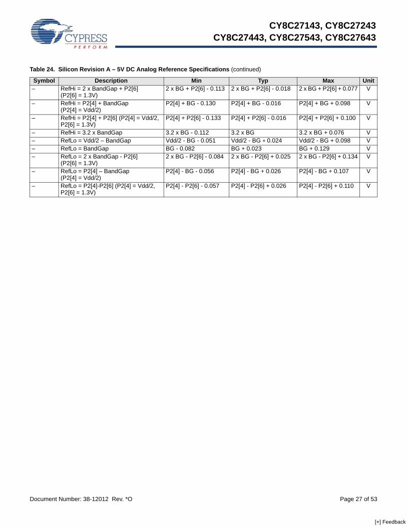
CY8C27143, CY8C27243CY8C27443, CY8C27543, CY8C27643
Document Number: 38-12012 Rev. *O Page 27 of 53
– RefHi = 2 x BandGap + P2[6] (P2[6] = 1.3V)
2 x BG + P2[6] - 0.113 2 x BG + P2[6] - 0.018 2 x BG + P2[6] + 0.077 V
– RefHi = P2[4] + BandGap (P2[4] = Vdd/2)
P2[4] + BG - 0.130 P2[4] + BG - 0.016 P2[4] + BG + 0.098 V
– RefHi = P2[4] + P2[6] (P2[4] = Vdd/2, P2[6] = 1.3V)
P2[4] + P2[6] - 0.133 P2[4] + P2[6] - 0.016 P2[4] + P2[6] + 0.100 V
– RefHi = 3.2 x BandGap 3.2 x BG - 0.112 3.2 x BG 3.2 x BG + 0.076 V– RefLo = Vdd/2 – BandGap Vdd/2 - BG - 0.051 Vdd/2 - BG + 0.024 Vdd/2 - BG + 0.098 V– RefLo = BandGap BG - 0.082 BG + 0.023 BG + 0.129 V– RefLo = 2 x BandGap - P2[6]
(P2[6] = 1.3V)2 x BG - P2[6] - 0.084 2 x BG - P2[6] + 0.025 2 x BG - P2[6] + 0.134 V
– RefLo = P2[4] – BandGap (P2[4] = Vdd/2)
P2[4] - BG - 0.056 P2[4] - BG + 0.026 P2[4] - BG + 0.107 V
– RefLo = P2[4]-P2[6] (P2[4] = Vdd/2, P2[6] = 1.3V)
P2[4] - P2[6] - 0.057 P2[4] - P2[6] + 0.026 P2[4] - P2[6] + 0.110 V
Table 24. Silicon Revision A – 5V DC Analog Reference Specifications (continued)
Symbol Description Min Typ Max Unit
[+] Feedback

CY8C27143, CY8C27243CY8C27443, CY8C27543, CY8C27643
Document Number: 38-12012 Rev. *O Page 28 of 53
Note7. AGND tolerance includes the offsets of the local buffer in the PSoC block.
Table 25. Silicon Revision B – 5V DC Analog Reference Specifications
Symbol Description Min Typ Max UnitBG Bandgap Voltage Reference 1.28 1.30 1.32 V– AGND = Vdd/2[7] Vdd/2 - 0.030 Vdd/2 Vdd/2 + 0.007 V– AGND = 2 x BandGap[7] 2 x BG - 0.043 2 x BG 2 x BG + 0.024 V– AGND = P2[4] (P2[4] = Vdd/2)[7] P2[4] - 0.011 P2[4] P2[4] + 0.011 V– AGND = BandGap[7] BG - 0.009 BG BG + 0.009 V– AGND = 1.6 x BandGap[7] 1.6 x BG - 0.018 1.6 x BG 1.6 x BG + 0.018 V– AGND Block to Block Variation
(AGND = Vdd/2)[7]-0.034 0.000 0.034 V
– RefHi = Vdd/2 + BandGap Vdd/2 + BG - 0.1 Vdd/2 + BG - 0.01 Vdd/2 + BG + 0.1 V– RefHi = 3 x BandGap 3 x BG - 0.06 3 x BG - 0.01 3 x BG + 0.06 V– RefHi = 2 x BandGap + P2[6]
(P2[6] = 1.3V)2 x BG + P2[6] - 0.06 2 x BG + P2[6] - 0.01 2 x BG + P2[6] + 0.06 V
– RefHi = P2[4] + BandGap (P2[4] = Vdd/2)
P2[4] + BG - 0.06 P2[4] + BG - 0.01 P2[4] + BG + 0.06 V
– RefHi = P2[4] + P2[6] (P2[4] = Vdd/2, P2[6] = 1.3V)
P2[4] + P2[6] - 0.06 P2[4] + P2[6] - 0.01 P2[4] + P2[6] + 0.06 V
– RefHi = 3.2 x BandGap 3.2 x BG - 0.06 3.2 x BG - 0.01 3.2 x BG + 0.06 V– RefLo = Vdd/2 – BandGap Vdd/2 - BG - 0.051 Vdd/2 - BG + 0.01 Vdd/2 - BG + 0.06 V– RefLo = BandGap BG - 0.06 BG + 0.01 BG + 0.06 V– RefLo = 2 x BandGap - P2[6]
(P2[6] = 1.3V)2 x BG - P2[6] - 0.04 2 x BG - P2[6] + 0.01 2 x BG - P2[6] + 0.04 V
– RefLo = P2[4] – BandGap (P2[4] = Vdd/2)
P2[4] - BG - 0.056 P2[4] - BG + 0.01 P2[4] - BG + 0.056 V
– RefLo = P2[4]-P2[6] (P2[4] = Vdd/2, P2[6] = 1.3V)
P2[4] - P2[6] - 0.056 P2[4] - P2[6] + 0.01 P2[4] - P2[6] + 0.056 V
Table 26. Silicon Revision A – 3.3V DC Analog Reference Specifications
Symbol Description Min Typ Max UnitBG Bandgap Voltage Reference 1.274 1.30 1.326 V– AGND = Vdd/2[8] Vdd/2 - 0.027 Vdd/2 - 0.003 Vdd/2 + 0.002 V– AGND = 2 x BandGap[8] Not Allowed– AGND = P2[4] (P2[4] = Vdd/2) P2[4] - 0.008 P2[4] + 0.001 P2[4] + 0.009 V– AGND = BandGap[8] BG - 0.009 BG BG + 0.009 V– AGND = 1.6 x BandGap[8] 1.6 x BG - 0.018 1.6 x BG 1.6 x BG + 0.018 V– AGND Block to Block Variation
(AGND = Vdd/2)[8]-0.034 0.000 0.034 V
– RefHi = Vdd/2 + BandGap Not Allowed– RefHi = 3 x BandGap Not Allowed– RefHi = 2 x BandGap + P2[6]
(P2[6] = 0.5V)Not Allowed
– RefHi = P2[4] + BandGap (P2[4] = Vdd/2)
Not Allowed
– RefHi = P2[4] + P2[6] (P2[4] = Vdd/2, P2[6] = 0.5V)
P2[4] + P2[6] - 0.075 P2[4] + P2[6] - 0.009 P2[4] + P2[6] + 0.057 V
– RefHi = 3.2 x BandGap Not Allowed– RefLo = Vdd/2 - BandGap Not Allowed
[+] Feedback
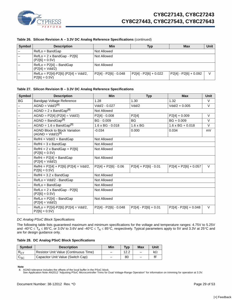
CY8C27143, CY8C27243CY8C27443, CY8C27543, CY8C27643
Document Number: 38-12012 Rev. *O Page 29 of 53
DC Analog PSoC Block SpecificationsThe following table lists guaranteed maximum and minimum specifications for the voltage and temperature ranges: 4.75V to 5.25Vand -40°C ≤ TA ≤ 85°C, or 3.0V to 3.6V and -40°C ≤ TA ≤ 85°C, respectively. Typical parameters apply to 5V and 3.3V at 25°C andare for design guidance only.
– RefLo = BandGap Not Allowed– RefLo = 2 x BandGap - P2[6]
(P2[6] = 0.5V)Not Allowed
– RefLo = P2[4] – BandGap (P2[4] = Vdd/2)
Not Allowed
– RefLo = P2[4]-P2[6] (P2[4] = Vdd/2, P2[6] = 0.5V)
P2[4] - P2[6] - 0.048 P2[4] - P2[6] + 0.022 P2[4] - P2[6] + 0.092 V
Table 26. Silicon Revision A – 3.3V DC Analog Reference Specifications (continued)
Symbol Description Min Typ Max Unit
Note8. AGND tolerance includes the offsets of the local buffer in the PSoC block.
See Application Note AN2012 “Adjusting PSoC Microcontroller Trims for Dual Voltage-Range Operation” for information on trimming for operation at 3.3V.
Table 27. Silicon Revision B – 3.3V DC Analog Reference Specifications
Symbol Description Min Typ Max UnitBG Bandgap Voltage Reference 1.28 1.30 1.32 V– AGND = Vdd/2[8] Vdd/2 - 0.027 Vdd/2 Vdd/2 + 0.005 V– AGND = 2 x BandGap[8] Not Allowed– AGND = P2[4] (P2[4] = Vdd/2) P2[4] - 0.008 P2[4] P2[4] + 0.009 V– AGND = BandGap[8] BG - 0.009 BG BG + 0.009 V– AGND = 1.6 x BandGap[8] 1.6 x BG - 0.018 1.6 x BG 1.6 x BG + 0.018 V– AGND Block to Block Variation
(AGND = Vdd/2)[8]-0.034 0.000 0.034 mV
– RefHi = Vdd/2 + BandGap Not Allowed– RefHi = 3 x BandGap Not Allowed– RefHi = 2 x BandGap + P2[6]
(P2[6] = 0.5V)Not Allowed
– RefHi = P2[4] + BandGap (P2[4] = Vdd/2)
Not Allowed
– RefHi = P2[4] + P2[6] (P2[4] = Vdd/2, P2[6] = 0.5V)
P2[4] + P2[6] - 0.06 P2[4] + P2[6] - 0.01 P2[4] + P2[6] + 0.057 V
– RefHi = 3.2 x BandGap Not Allowed– RefLo = Vdd/2 - BandGap Not Allowed– RefLo = BandGap Not Allowed– RefLo = 2 x BandGap - P2[6]
(P2[6] = 0.5V)Not Allowed
– RefLo = P2[4] – BandGap (P2[4] = Vdd/2)
Not Allowed
– RefLo = P2[4]-P2[6] (P2[4] = Vdd/2, P2[6] = 0.5V)
P2[4] - P2[6] - 0.048 P2[4] - P2[6] + 0.01 P2[4] - P2[6] + 0.048 V
Table 28. DC Analog PSoC Block Specifications
Symbol Description Min Typ Max UnitRCT Resistor Unit Value (Continuous Time) – 12.2 – kΩCSC Capacitor Unit Value (Switch Cap) – 80 – fF
[+] Feedback
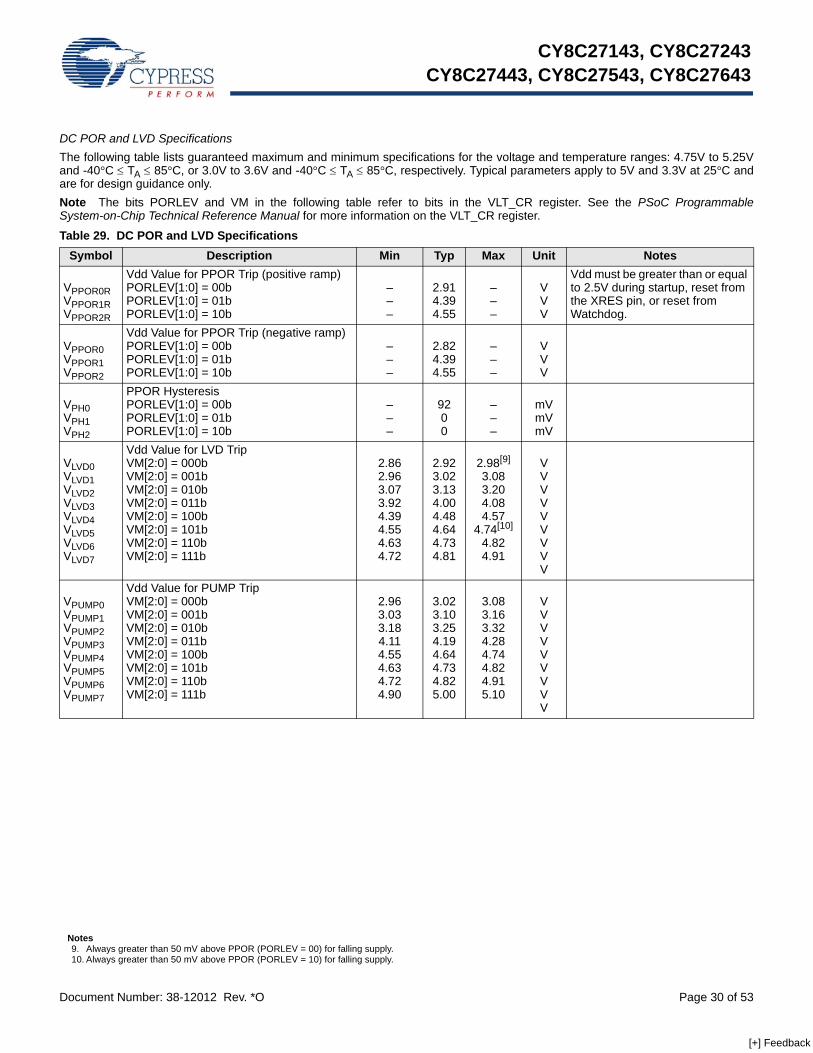
CY8C27143, CY8C27243CY8C27443, CY8C27543, CY8C27643
Document Number: 38-12012 Rev. *O Page 30 of 53
DC POR and LVD SpecificationsThe following table lists guaranteed maximum and minimum specifications for the voltage and temperature ranges: 4.75V to 5.25Vand -40°C ≤ TA ≤ 85°C, or 3.0V to 3.6V and -40°C ≤ TA ≤ 85°C, respectively. Typical parameters apply to 5V and 3.3V at 25°C andare for design guidance only.Note The bits PORLEV and VM in the following table refer to bits in the VLT_CR register. See the PSoC ProgrammableSystem-on-Chip Technical Reference Manual for more information on the VLT_CR register.
Table 29. DC POR and LVD SpecificationsSymbol Description Min Typ Max Unit Notes
VPPOR0RVPPOR1RVPPOR2R
Vdd Value for PPOR Trip (positive ramp)PORLEV[1:0] = 00bPORLEV[1:0] = 01bPORLEV[1:0] = 10b
–––
2.914.394.55
–––
VVV
Vdd must be greater than or equal to 2.5V during startup, reset from the XRES pin, or reset from Watchdog.
VPPOR0VPPOR1VPPOR2
Vdd Value for PPOR Trip (negative ramp)PORLEV[1:0] = 00bPORLEV[1:0] = 01bPORLEV[1:0] = 10b
–––
2.824.394.55
–––
VVV
VPH0VPH1VPH2
PPOR HysteresisPORLEV[1:0] = 00bPORLEV[1:0] = 01bPORLEV[1:0] = 10b
–––
9200
–––
mVmVmV
VLVD0VLVD1VLVD2VLVD3VLVD4VLVD5VLVD6VLVD7
Vdd Value for LVD TripVM[2:0] = 000bVM[2:0] = 001bVM[2:0] = 010bVM[2:0] = 011bVM[2:0] = 100bVM[2:0] = 101bVM[2:0] = 110bVM[2:0] = 111b
2.862.963.073.924.394.554.634.72
2.923.023.134.004.484.644.734.81
2.98[9]
3.083.204.084.57
4.74[10]
4.824.91
V
VVVVVVVV
VPUMP0VPUMP1VPUMP2VPUMP3VPUMP4VPUMP5VPUMP6VPUMP7
Vdd Value for PUMP TripVM[2:0] = 000bVM[2:0] = 001bVM[2:0] = 010bVM[2:0] = 011bVM[2:0] = 100bVM[2:0] = 101bVM[2:0] = 110bVM[2:0] = 111b
2.963.033.184.114.554.634.724.90
3.023.103.254.194.644.734.825.00
3.083.163.324.284.744.824.915.10
VVVVVVVVV
Notes9. Always greater than 50 mV above PPOR (PORLEV = 00) for falling supply.10. Always greater than 50 mV above PPOR (PORLEV = 10) for falling supply.
[+] Feedback

CY8C27143, CY8C27243CY8C27443, CY8C27543, CY8C27643
Document Number: 38-12012 Rev. *O Page 31 of 53
DC Programming SpecificationsThe following table lists guaranteed maximum and minimum specifications for the voltage and temperature ranges: 4.75V to 5.25Vand -40°C ≤ TA ≤ 85°C, or 3.0V to 3.6V and -40°C ≤ TA ≤ 85°C, respectively. Typical parameters apply to 5V and 3.3V at 25°C andare for design guidance only.
Table 30. DC Programming Specifications
Symbol Description Min Typ Max Unit NotesIDDP Supply Current During Programming or Verify – 5 25 mAVILP Input Low Voltage During Programming or
Verify– – 0.8 V
VIHP Input High Voltage During Programming or Verify
2.2 – – V
IILP Input Current when Applying Vilp to P1[0] or P1[1] During Programming or Verify
– – 0.2 mA Driving internal pull down resistor.
IIHP Input Current when Applying Vihp to P1[0] or P1[1] During Programming or Verify
– – 1.5 mA Driving internal pull down resistor.
VOLV Output Low Voltage During Programming or Verify
– – Vss + 0.75
V
VOHV Output High Voltage During Programming or Verify
Vdd - 1.0 – Vdd V
FlashENPB Flash Endurance (per block) 50,000[11] – – Cycles Erase/write cycles per block.
FlashENT Flash Endurance (total)[12] 1,800,000 – – Cycles Erase/write cycles.FlashDR Flash Data Retention 10 – – Years
Notes11. The 50,000 cycle flash endurance per block will only be guaranteed if the flash is operating within one voltage range. Voltage ranges are 3.0V to 3.6V and 4.75V
to 5.25V.12. A maximum of 36 x 50,000 block endurance cycles is allowed. This may be balanced between operations on 36x1 blocks of 50,000 maximum cycles each, 36x2
blocks of 25,000 maximum cycles each, or 36x4 blocks of 12,500 maximum cycles each (to limit the total number of cycles to 36x50,000 and that no single block ever sees more than 50,000 cycles).For the full industrial range, the user must employ a temperature sensor user module (FlashTemp) and feed the result to the temperature argument before writing. Refer to the Flash APIs Application Note AN2015 at http://www.cypress.com under Application Notes for more information
[+] Feedback

CY8C27143, CY8C27243CY8C27443, CY8C27543, CY8C27643
Document Number: 38-12012 Rev. *O Page 32 of 53
AC Electrical Characteristics
AC Chip-Level SpecificationsThe following table lists guaranteed maximum and minimum specifications for the voltage and temperature ranges: 4.75V to 5.25Vand -40°C ≤ TA ≤ 85°C, or 3.0V to 3.6V and -40°C ≤ TA ≤ 85°C, respectively. Typical parameters apply to 5V and 3.3V at 25°C andare for design guidance only.
Table 31. AC Chip-Level Specifications
Symbol Description Min Typ Max Unit NotesFIMO Internal Main Oscillator Frequency 23.4 24 24.6[13] MHz Trimmed. Utilizing factory trim
values.FCPU1 CPU Frequency (5V Nominal) 0.93 24 24.6[13,14] MHz Trimmed. Utilizing factory trim
values.FCPU2 CPU Frequency (3.3V Nominal) 0.93 12 12.3[14,15] MHz Trimmed. Utilizing factory trim
values.F48M Digital PSoC Block Frequency 0 48 49.2[13,14, 16] MHz Refer to the AC Digital Block
Specifications below.F24M Digital PSoC Block Frequency 0 24 24.6[14, 16] MHzF32K1 Internal Low Speed Oscillator
Frequency15 32 64 kHz
F32K2 External Crystal Oscillator – 32.768 – kHz Accuracy is capacitor and crystal dependent. 50% duty cycle.
F32K_U Internal Low Speed Oscillator (ILO) Untrimmed Frequency
5 – – kHz After a reset and before the m8c starts to run, the ILO is not trimmed. See the System Resets section of the PSoC Technical Reference Manual for details on timing this
FPLL PLL Frequency – 23.986 – MHz Multiple (x732) of crystal frequency.
Jitter24M2 24 MHz Period Jitter (PLL) – – 600 psTPLLSLEW PLL Lock Time 0.5 – 10 msTPLLSLEWSLOW PLL Lock Time for Low Gain Setting 0.5 – 50 msTOS External Crystal Oscillator Startup to
1%– 1700 2620 ms
TOSACC External Crystal Oscillator Startup to 100 ppm
– 2800 3800 ms The crystal oscillator frequency is within 100 ppm of its final value by the end of the Tosacc period. Correct operation assumes a properly loaded 1 µW maximum drive level 32.768 kHz crystal. 3.0V ≤ Vdd ≤ 5.5V, -40°C ≤ TA ≤ 85°C.
Jitter32k 32 kHz Period Jitter – 100 – nsTXRST External Reset Pulse Width 10 – – μsDC24M 24 MHz Duty Cycle 40 50 60 %DCILO Internal Low Speed Oscillator Duty
Cycle20 50 80 %
Step24M 24 MHz Trim Step Size – 50 – kHz
Notes13. 4.75V < Vdd < 5.25V.14. Accuracy derived from Internal Main Oscillator with appropriate trim for Vdd range.15. 3.0V < Vdd < 3.6V. See Application Note AN2012 “Adjusting PSoC Microcontroller Trims for Dual Voltage-Range Operation” for information on trimming for operation
at 3.3V.16. See the individual user module data sheets for information on maximum frequencies for user modules.
[+] Feedback

CY8C27143, CY8C27243CY8C27443, CY8C27543, CY8C27643
Document Number: 38-12012 Rev. *O Page 33 of 53
Figure 12. PLL Lock Timing Diagram
Figure 13. PLL Lock for Low Gain Setting Timing Diagram
Figure 14. External Crystal Oscillator Startup Timing Diagram
Figure 15. 24 MHz Period Jitter (IMO) Timing Diagram
Figure 16. 32 kHz Period Jitter (ECO) Timing Diagram
TPOWERUP Time from end of POR to CPU executing code
– 16 100 ms Power up from 0V. See the System Resets section of the PSoC Technical Reference Manual.
Fout48M 48 MHz Output Frequency 46.8 48.0 49.2[13,15] MHz Trimmed. Utilizing factory trim values.
Jitter24M1 24 MHz Period Jitter (IMO) – 600 – psFMAX Maximum frequency of signal on row
input or row output.– – 12.3 MHz
SRPOWER_UP Power Supply Slew Rate – – 250 V/ms Vdd slew rate during power up.
Table 31. AC Chip-Level Specifications (continued)
Symbol Description Min Typ Max Unit Notes
24 MHz
FPLL
PLLEnable
TPLLSLEW
PLLGain 0
24 MHz
FPLL
PLLEnable
TPLLSLEWLOW
PLLGain 1
32 kHz
F32K2
32KSelect
TOS
Jitter24M1
F24M
Jitter32k
F32K2
[+] Feedback

CY8C27143, CY8C27243CY8C27443, CY8C27543, CY8C27643
Document Number: 38-12012 Rev. *O Page 34 of 53
AC General Purpose I/O SpecificationsThe following table lists guaranteed maximum and minimum specifications for the voltage and temperature ranges: 4.75V to 5.25Vand -40°C ≤ TA ≤ 85°C, or 3.0V to 3.6V and -40°C ≤ TA ≤ 85°C, respectively. Typical parameters apply to 5V and 3.3V at 25°C andare for design guidance only.
Figure 17. GPIO Timing Diagram
AC Operational Amplifier SpecificationsThe following tables list guaranteed maximum and minimum specifications for the voltage and temperature ranges: 4.75V to 5.25Vand -40°C ≤ TA ≤ 85°C, or 3.0V to 3.6V and -40°C ≤ TA ≤ 85°C, respectively. Typical parameters apply to 5V and 3.3V at 25°C andare for design guidance only.Settling times, slew rates, and gain bandwidth are based on the Analog Continuous Time PSoC block.Power = High and Opamp Bias = High is not supported at 3.3V.
Table 32. AC GPIO SpecificationsSymbol Description Min Typ Max Unit Notes
FGPIO GPIO Operating Frequency 0 – 12 MHz Normal Strong ModeTRiseF Rise Time, Normal Strong Mode, Cload = 50 pF 3 – 18 ns Vdd = 4.5 to 5.25V, 10% - 90%TFallF Fall Time, Normal Strong Mode, Cload = 50 pF 2 – 18 ns Vdd = 4.5 to 5.25V, 10% - 90%TRiseS Rise Time, Slow Strong Mode, Cload = 50 pF 10 27 – ns Vdd = 3 to 5.25V, 10% - 90%TFallS Fall Time, Slow Strong Mode, Cload = 50 pF 10 22 – ns Vdd = 3 to 5.25V, 10% - 90%
TFallFTFallS
TRiseFTRiseS
90%
10%
GPIOPin
OutputVoltage
Table 33. 5V AC Operational Amplifier SpecificationsSymbol Description Min Typ Max Unit
TROA Rising Settling Time from 80% of ΔV to 0.1% of ΔV (10 pF load, Unity Gain)Power = Low, Opamp Bias = LowPower = Medium, Opamp Bias = HighPower = High, Opamp Bias = High
–––
–––
3.90.720.62
μsμsμs
TSOA Falling Settling Time from 20% of ΔV to 0.1% of ΔV (10 pF load, Unity Gain)Power = Low, Opamp Bias = LowPower = Medium, Opamp Bias = HighPower = High, Opamp Bias = High
–––
–––
5.90.920.72
μsμsμs
SRROA Rising Slew Rate (20% to 80%)(10 pF load, Unity Gain)Power = Low, Opamp Bias = LowPower = Medium, Opamp Bias = HighPower = High, Opamp Bias = High
0.151.76.5
–––
–––
V/μsV/μsV/μs
SRFOA Falling Slew Rate (20% to 80%)(10 pF load, Unity Gain)Power = Low, Opamp Bias = LowPower = Medium, Opamp Bias = HighPower = High, Opamp Bias = High
0.010.54.0
–––
–––
V/μsV/μsV/μs
[+] Feedback
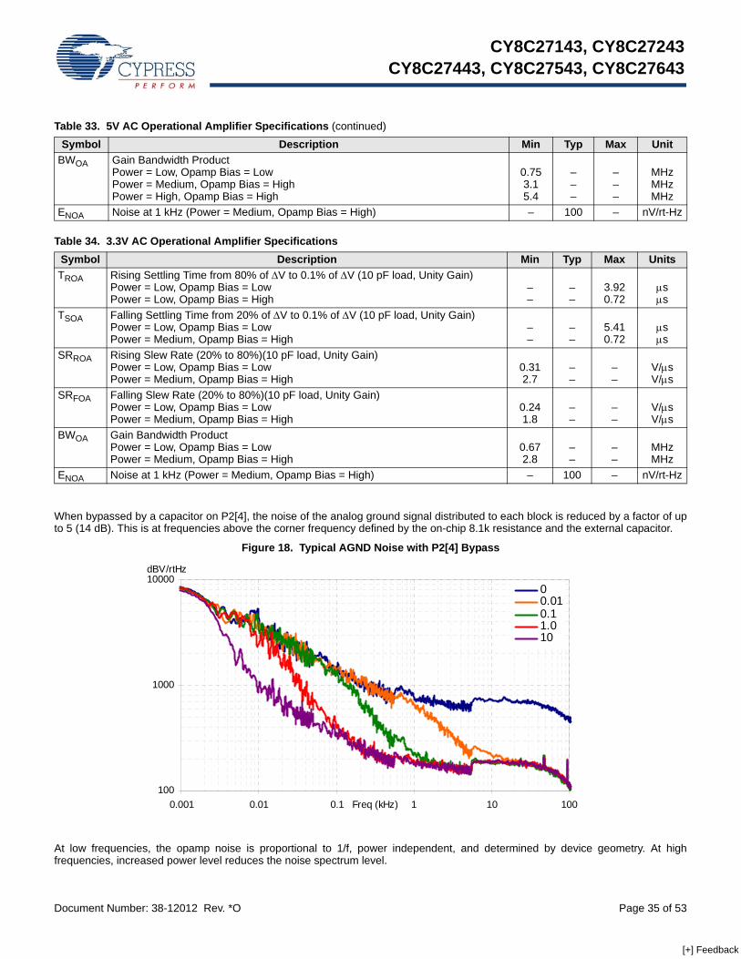
CY8C27143, CY8C27243CY8C27443, CY8C27543, CY8C27643
Document Number: 38-12012 Rev. *O Page 35 of 53
When bypassed by a capacitor on P2[4], the noise of the analog ground signal distributed to each block is reduced by a factor of upto 5 (14 dB). This is at frequencies above the corner frequency defined by the on-chip 8.1k resistance and the external capacitor.
Figure 18. Typical AGND Noise with P2[4] Bypass
At low frequencies, the opamp noise is proportional to 1/f, power independent, and determined by device geometry. At highfrequencies, increased power level reduces the noise spectrum level.
BWOA Gain Bandwidth Product Power = Low, Opamp Bias = LowPower = Medium, Opamp Bias = HighPower = High, Opamp Bias = High
0.753.15.4
–––
–––
MHzMHzMHz
ENOA Noise at 1 kHz (Power = Medium, Opamp Bias = High) – 100 – nV/rt-Hz
Table 33. 5V AC Operational Amplifier Specifications (continued)
Symbol Description Min Typ Max Unit
Table 34. 3.3V AC Operational Amplifier SpecificationsSymbol Description Min Typ Max UnitsTROA Rising Settling Time from 80% of ΔV to 0.1% of ΔV (10 pF load, Unity Gain)
Power = Low, Opamp Bias = LowPower = Low, Opamp Bias = High
––
––
3.920.72
μsμs
TSOA Falling Settling Time from 20% of ΔV to 0.1% of ΔV (10 pF load, Unity Gain)Power = Low, Opamp Bias = LowPower = Medium, Opamp Bias = High
––
––
5.410.72
μsμs
SRROA Rising Slew Rate (20% to 80%)(10 pF load, Unity Gain)Power = Low, Opamp Bias = LowPower = Medium, Opamp Bias = High
0.312.7
––
––
V/μsV/μs
SRFOA Falling Slew Rate (20% to 80%)(10 pF load, Unity Gain)Power = Low, Opamp Bias = LowPower = Medium, Opamp Bias = High
0.241.8
––
––
V/μsV/μs
BWOA Gain Bandwidth Product Power = Low, Opamp Bias = LowPower = Medium, Opamp Bias = High
0.672.8
––
––
MHzMHz
ENOA Noise at 1 kHz (Power = Medium, Opamp Bias = High) – 100 – nV/rt-Hz
100
1000
10000
0.001 0.01 0.1 1 10 100Freq (kHz)
dBV/rtHz
00.010.11.010
[+] Feedback

CY8C27143, CY8C27243CY8C27443, CY8C27543, CY8C27643
Document Number: 38-12012 Rev. *O Page 36 of 53
Figure 19. Typical Opamp Noise
AC Low Power Comparator SpecificationsThe following table lists guaranteed maximum and minimum specifications for the voltage and temperature ranges: 4.75V to 5.25Vand -40°C ≤ TA ≤ 85°C, 3.0V to 3.6V and -40°C ≤ TA ≤ 85°C, or 2.4V to 3.0V and -40°C ≤ TA ≤ 85°C, respectively. Typical parametersapply to 5V at 25°C and are for design guidance only.
AC Digital Block SpecificationsThe following table lists guaranteed maximum and minimum specifications for the voltage and temperature ranges: 4.75V to 5.25Vand -40°C ≤ TA ≤ 85°C, or 3.0V to 3.6V and -40°C ≤ TA ≤ 85°C, respectively. Typical parameters apply to 5V and 3.3V at 25°C andare for design guidance only.
10
100
1000
10000
0.001 0.01 0.1 1 10 100Freq (kHz)
nV/rtHz
PH_BHPH_BLPM_BLPL_BL
Table 35. AC Low Power Comparator SpecificationsSymbol Description Min Typ Max Unit Notes
TRLPC LPC response time – – 50 μs ≥ 50 mV overdrive comparator reference set within VREFLPC.
Table 36. AC Digital Block Specifications
Function Description Min Typ Max Unit NotesAll Functions
Maximum Block Clocking Frequency (> 4.75V) – – 49.2 MHz 4.75V < Vdd < 5.25VMaximum Block Clocking Frequency (< 4.75V) – – 24.6 MHz 3.0V < Vdd < 4.75V
Timer Capture Pulse Width 50[17] – – nsMaximum Frequency, No Capture – – 49.2 MHz 4.75V < Vdd < 5.25VMaximum Frequency, With Capture – – 24.6 MHz
Counter Enable Pulse Width 50[17] – – nsMaximum Frequency, No Enable Input – – 49.2 MHz 4.75V < Vdd < 5.25VMaximum Frequency, Enable Input – – 24.6 MHz
Notes17. 50 ns minimum input pulse width is based on the input synchronizers running at 24 MHz (42 ns nominal period).18. Refer to Table 47 on page 50
[+] Feedback
CY8C27143, CY8C27243CY8C27443, CY8C27543, CY8C27643
Document Number: 38-12012 Rev. *O Page 37 of 53
AC Analog Output Buffer SpecificationsThe following tables list guaranteed maximum and minimum specifications for the voltage and temperature ranges: 4.75V to 5.25Vand -40°C ≤ TA ≤ 85°C, or 3.0V to 3.6V and -40°C ≤ TA ≤ 85°C, respectively. Typical parameters apply to 5V and 3.3V at 25°C andare for design guidance only.
Dead Band
Kill Pulse Width:Asynchronous Restart Mode 20 – – nsSynchronous Restart Mode 50[17] – – nsDisable Mode 50[17] – – ns
Maximum Frequency – – 49.2 MHz 4.75V < Vdd < 5.25VCRCPRS(PRS Mode)
Maximum Input Clock Frequency – – 49.2 MHz 4.75V < Vdd < 5.25V
CRCPRS(CRC Mode)
Maximum Input Clock Frequency – – 24.6 MHz
SPIM Maximum Input Clock Frequency – – 8.2 MHz Maximum data rate at 4.1 MHz due to 2 x over clocking.
SPIS Maximum Input Clock Frequency – – 4.1 MHzWidth of SS_ Negated Between Transmis-sions
50[17] – – MHz
Trans-mitter
Maximum Input Clock Frequency [17]
Silicon A
Silicon B
Silicon B Maximum Input Clock Frequency with Vdd ≥ 4.75V, 2 Stop Bits
–
–
–
–
–
–
16.4
24.6
49.2
MHz
MHz
MHz
Maximum data rate at 2.05 MHz due to 8 x over clocking.Maximum data rate at 3.08 MHz due to 8 x over clocking.Maximum data rate at 6.15 MHz due to 8 x over clocking.
Receiver Maximum Input Clock Frequency [18]
Silicon A
Silicon B
Silicon B Maximum Input Clock Frequency with Vdd ≥ 4.75V, 2 Stop Bits
–
–
–
–
–
–
16.4
24.6
49.2
MHz
MHz
MHz
Maximum data rate at 2.05 MHz due to 8 x over clocking.Maximum data rate at 3.08 MHz due to 8 x over clocking.Maximum data rate at 6.15 MHz due to 8 x over clocking.
Table 36. AC Digital Block Specifications (continued)
Function Description Min Typ Max Unit Notes
Table 37. 5V AC Analog Output Buffer Specifications
Symbol Description Min Typ Max UnitTROB Rising Settling Time to 0.1%, 1V Step, 100 pF Load
Power = Low Power = High
––
––
2.52.5
μsμs
TSOB Falling Settling Time to 0.1%, 1V Step, 100 pF Load Power = Low Power = High
––
––
2.22.2
μsμs
[+] Feedback
CY8C27143, CY8C27243CY8C27443, CY8C27543, CY8C27643
Document Number: 38-12012 Rev. *O Page 38 of 53
AC External Clock SpecificationsThe following tables list guaranteed maximum and minimum specifications for the voltage and temperature ranges: 4.75V to 5.25Vand -40°C ≤ TA ≤ 85°C, or 3.0V to 3.6V and -40°C ≤ TA ≤ 85°C, respectively. Typical parameters apply to 5V and 3.3V at 25°C andare for design guidance only.
SRROB Rising Slew Rate (20% to 80%), 1V Step, 100 pF Load Power = Low Power = High
0.650.65
––
––
V/μsV/μs
SRFOB Falling Slew Rate (80% to 20%), 1V Step, 100 pF Load Power = Low Power = High
0.650.65
––
––
V/μsV/μs
BWOB Small Signal Bandwidth, 20mVpp, 3dB BW, 100 pF Load Power = Low Power = High
0.80.8
––
––
MHzMHz
BWOB Large Signal Bandwidth, 1Vpp, 3dB BW, 100 pF Load Power = Low Power = High
300300
––
––
kHzkHz
Table 37. 5V AC Analog Output Buffer Specifications (continued)
Symbol Description Min Typ Max Unit
Table 38. 3.3V AC Analog Output Buffer Specifications
Symbol Description Min Typ Max UnitTROB Rising Settling Time to 0.1%, 1V Step, 100 pF Load
Power = Low Power = High
––
––
3.83.8
μsμs
TSOB Falling Settling Time to 0.1%, 1V Step, 100 pF Load Power = Low Power = High
––
––
2.62.6
μsμs
SRROB Rising Slew Rate (20% to 80%), 1V Step, 100 pF Load Power = Low Power = High
0.50.5
––
––
V/μsV/μs
SRFOB Falling Slew Rate (80% to 20%), 1V Step, 100 pF Load Power = Low Power = High
0.50.5
––
––
V/μsV/μs
BWOB Small Signal Bandwidth, 20mVpp, 3dB BW, 100 pF Load Power = Low Power = High
0.70.7
––
––
MHzMHz
BWOB Large Signal Bandwidth, 1Vpp, 3dB BW, 100 pF Load Power = Low Power = High
200200
––
––
kHzkHz
Table 39. 5V AC External Clock SpecificationsSymbol Description Min Typ Max Unit
FOSCEXT Frequency 0.093 – 24.6 MHz– High Period 20.6 – 5300 ns– Low Period 20.6 – – ns– Power Up IMO to Switch 150 – – μs
Notes19. Maximum CPU frequency is 12 MHz at 3.3V. With the CPU clock divider set to 1, the external clock must adhere to the maximum frequency and duty cycle
requirements.20. If the frequency of the external clock is greater than 12 MHz, the CPU clock divider must be set to 2 or greater. In this case, the CPU clock divider ensures that the
fifty percent duty cycle requirement is met.21. For the full industrial range, the user must employ a temperature sensor user module (FlashTemp) and feed the result to the temperature argument before writing.
Refer to the Flash APIs Application Note AN2015 at http://www.cypress.com under Application Notes for more information.
[+] Feedback
CY8C27143, CY8C27243CY8C27443, CY8C27543, CY8C27643
Document Number: 38-12012 Rev. *O Page 39 of 53
AC Programming SpecificationsThe following table lists guaranteed maximum and minimum specifications for the voltage and temperature ranges: 4.75V to 5.25Vand -40°C ≤ TA ≤ 85°C, or 3.0V to 3.6V and -40°C ≤ TA ≤ 85°C, respectively. Typical parameters apply to 5V and 3.3V at 25°C andare for design guidance only.
AC I2C SpecificationsThe following table lists guaranteed maximum and minimum specifications for the voltage and temperature ranges: 4.75V to 5.25Vand -40°C ≤ TA ≤ 85°C, or 3.0V to 3.6V and -40°C ≤ TA ≤ 85°C, respectively. Typical parameters apply to 5V and 3.3V at 25°C andare for design guidance only.
Table 40. 3.3V AC External Clock SpecificationsSymbol Description Min Typ Max Unit
FOSCEXT Frequency with CPU Clock divide by 1[19] 0.093 – 12.3 MHzFOSCEXT Frequency with CPU Clock divide by 2 or greater[20] 0.186 – 24.6 MHz– High Period with CPU Clock divide by 1 41.7 – 5300 ns– Low Period with CPU Clock divide by 1 41.7 – – ns– Power Up IMO to Switch 150 – – μs
Table 41. AC Programming Specifications
Symbol Description Min Typ Max Unit NotesTRSCLK Rise Time of SCLK 1 – 20 nsTFSCLK Fall Time of SCLK 1 – 20 nsTSSCLK Data Set up Time to Falling Edge of SCLK 40 – – nsTHSCLK Data Hold Time from Falling Edge of SCLK 40 – – nsFSCLK Frequency of SCLK 0 – 8 MHzTERASEB Flash Erase Time (Block) – 30 – msTWRITE Flash Block Write Time – 10 – msTDSCLK Data Out Delay from Falling Edge of SCLK – – 45 ns Vdd > 3.6TDSCLK3 Data Out Delay from Falling Edge of SCLK – – 50 ns 3.0 ≤ Vdd ≤ 3.6TERASEALL Flash Erase Time (Bulk) – 95 – ms Erase all Blocks and
protection fields at onceTPROGRAM_HOT Flash Block Erase + Flash Block Write Time – – 80[21] ms 0°C <= Tj <= 100°CTPROGRAM_COLD Flash Block Erase + Flash Block Write Time – – 160[21] ms -40°C <= Tj <= 0°C
Table 42. AC Characteristics of the I2C SDA and SCL Pins
Symbol DescriptionStandard Mode Fast Mode
UnitMin Max Min Max
FSCLI2C SCL Clock Frequency 0 100 0 400 kHzTHDSTAI2C Hold Time (repeated) START Condition. After this period, the first
clock pulse is generated.4.0 – 0.6 – μs
TLOWI2C LOW Period of the SCL Clock 4.7 – 1.3 – μsTHIGHI2C HIGH Period of the SCL Clock 4.0 – 0.6 – μsTSUSTAI2C Set-up Time for a Repeated START Condition 4.7 – 0.6 – μsTHDDATI2C Data Hold Time 0 – 0 – μs
Note22. A Fast-Mode I2C-bus device can be used in a Standard-Mode I2C-bus system, but the requirement tSU;DAT ≥ 250 ns must then be met. This is automatically the
case if the device does not stretch the LOW period of the SCL signal. If such device does stretch the LOW period of the SCL signal, it must output the next data bit to the SDA line trmax + tSU;DAT = 1000 + 250 = 1250 ns (according to the Standard-Mode I2C-bus specification) before the SCL line is released.
[+] Feedback

CY8C27143, CY8C27243CY8C27443, CY8C27543, CY8C27643
Document Number: 38-12012 Rev. *O Page 40 of 53
Figure 20. Definition for Timing for Fast/Standard Mode on the I2C Bus
TSUDATI2C Data Set-up Time 250 – 100[22] – nsTSUSTOI2C Set-up Time for STOP Condition 4.0 – 0.6 – μsTBUFI2C Bus Free Time Between a STOP and START Condition 4.7 – 1.3 – μsTSPI2C Pulse Width of spikes are suppressed by the input filter. – – 0 50 ns
Table 42. AC Characteristics of the I2C SDA and SCL Pins
Symbol DescriptionStandard Mode Fast Mode
UnitMin Max Min Max
SDA
SCL
S Sr SP
TBUFI2C
TSPI2CTHDSTAI2C
TSUSTOI2CTSUSTAI2C
TLOWI2C
THIGHI2CTHDDATI2CTHDSTAI2C
TSUDATI2C
[+] Feedback

CY8C27143, CY8C27243CY8C27443, CY8C27543, CY8C27643
Document Number: 38-12012 Rev. *O Page 41 of 53
Packaging InformationThis section illustrates the packaging specifications for the CY8C27x43 PSoC device, along with the thermal impedances for eachpackage and the typical package capacitance on crystal pins.Important Note Emulation tools may require a larger area on the target PCB than the chip’s footprint. For a detailed description ofthe emulation tools’ dimensions, refer to the document titled PSoC Emulator Pod Dimensions at http://www.cypress.com/design/MR10161.
Packaging DimensionsFigure 21. 8-Pin (300-Mil) PDIP
51-85075 *A
[+] Feedback
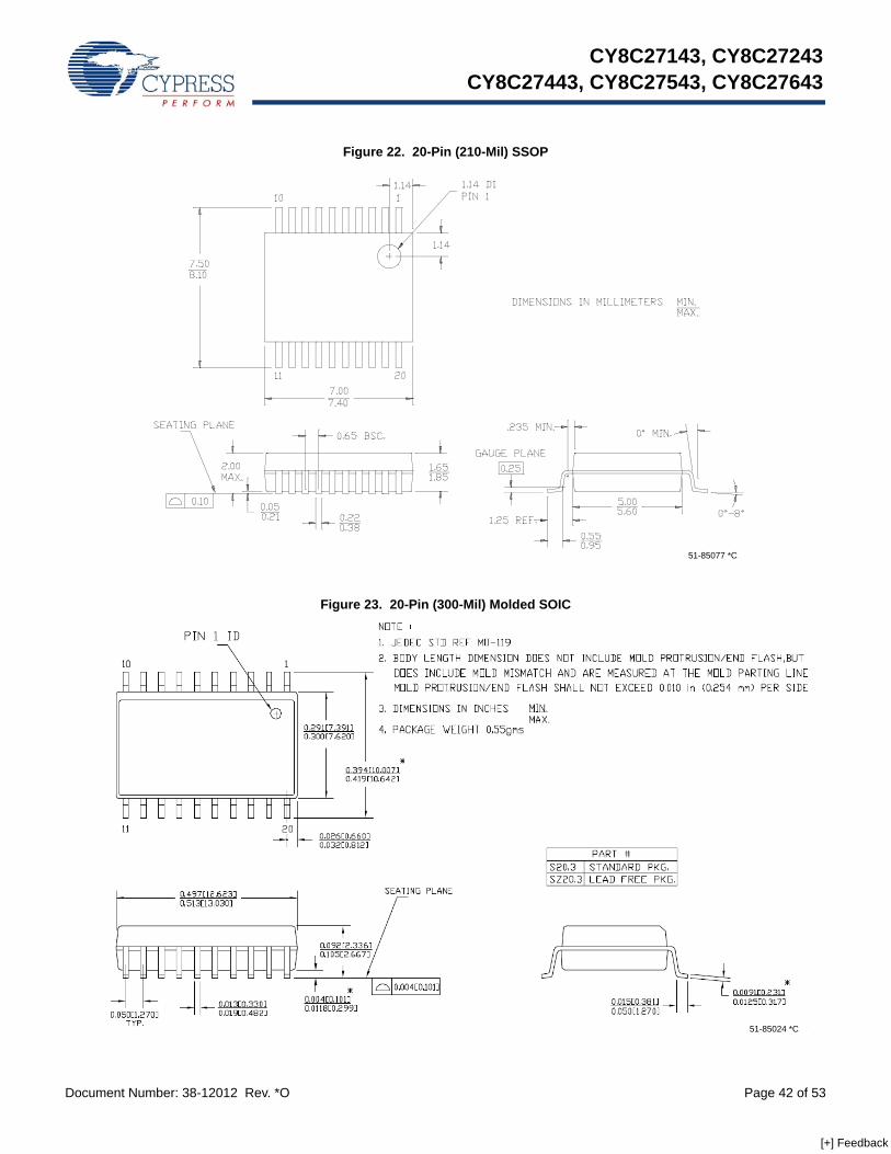
CY8C27143, CY8C27243CY8C27443, CY8C27543, CY8C27643
Document Number: 38-12012 Rev. *O Page 42 of 53
Figure 22. 20-Pin (210-Mil) SSOP
Figure 23. 20-Pin (300-Mil) Molded SOIC
51-85077 *C
51-85024 *C
[+] Feedback

CY8C27143, CY8C27243CY8C27443, CY8C27543, CY8C27643
Document Number: 38-12012 Rev. *O Page 43 of 53
Figure 24. 28-Pin (300-Mil) Molded DIP
Figure 25. 28-Pin (210-Mil) SSOP
DIMENSIONS IN INCHES[MM] MIN.MAX.
SEATING PLANE
0.260[6.60]0.295[7.49]
0.090[2.28]0.110[2.79]
0.055[1.39]0.065[1.65]
0.015[0.38]0.020[0.50]
0.015[0.38]0.060[1.52]
0.120[3.05]0.140[3.55]
0.009[0.23]0.012[0.30]
0.310[7.87]0.385[9.78]
0.290[7.36]0.325[8.25]
0.030[0.76]0.080[2.03]
0.115[2.92]0.160[4.06]
0.140[3.55]0.190[4.82]
1.345[34.16]1.385[35.18]
3° MIN.
114
15 28
REFERENCE JEDEC MO-095
PART #P28.3 STANDARD PKG.
LEAD FREE PKG.PZ28.3
LEAD END OPTION
SEE LEAD END OPTION
SEE LEAD END OPTION
(LEAD #1, 14, 15 & 28)
PACKAGE WEIGHT: 2.15gms
51-85014 *E
51-85079 *C
[+] Feedback

CY8C27143, CY8C27243CY8C27443, CY8C27543, CY8C27643
Document Number: 38-12012 Rev. *O Page 44 of 53
Figure 26. 28-Pin (300-Mil) Molded SOIC
Figure 27. 44-Pin TQFP
51-85026 *D
51-85064 *C
[+] Feedback
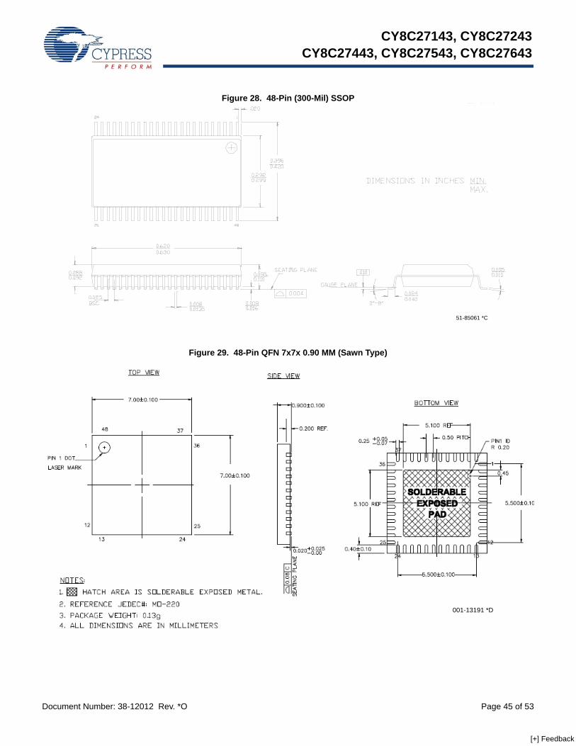
CY8C27143, CY8C27243CY8C27443, CY8C27543, CY8C27643
Document Number: 38-12012 Rev. *O Page 45 of 53
Figure 28. 48-Pin (300-Mil) SSOP
Figure 29. 48-Pin QFN 7x7x 0.90 MM (Sawn Type)
51-85061-C 51-85061 *C
001-13191 *D
[+] Feedback

CY8C27143, CY8C27243CY8C27443, CY8C27543, CY8C27643
Document Number: 38-12012 Rev. *O Page 46 of 53
Figure 30. 48-Pin (7x7 mm) QFN
Important Note For information on the preferred dimensions for mounting QFN packages, see the following Application Note athttp://www.amkor.com/products/notes_papers/MLFAppNote.pdf.
Thermal Impedances Capacitance on Crystal Pins
51-85152 *C
Table 43. Thermal Impedances per Package
Package Typical θJA *8 PDIP 120 oC/W
20 SSOP 116 oC/W20 SOIC 79 oC/W28 PDIP 67 oC/W28 SSOP 95 oC/W28 SOIC 68 oC/W44 TQFP 61 oC/W48 SSOP 69 oC/W48 QFN 18 oC/W
* TJ = TA + POWER x θJA
Table 44. Typical Package Capacitance on Crystal Pins
Package Package Capacitance8 PDIP 2.8 pF
20 SSOP 2.6 pF20 SOIC 2.5 pF28 PDIP 3.5 pF28 SSOP 2.8 pF28 SOIC 2.7 pF44 TQFP 2.6 pF48 SSOP 3.3 pF48 QFN 2.3 pF
[+] Feedback
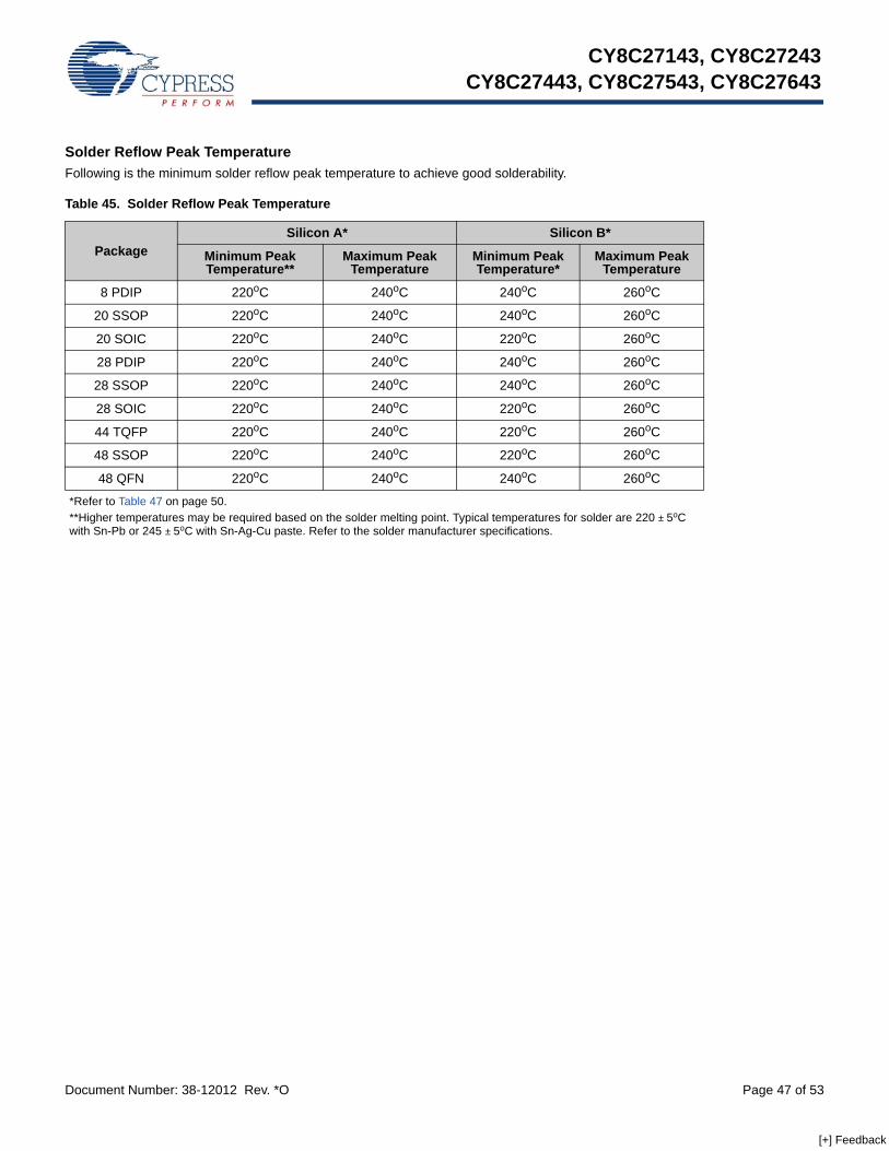
CY8C27143, CY8C27243CY8C27443, CY8C27543, CY8C27643
Document Number: 38-12012 Rev. *O Page 47 of 53
Solder Reflow Peak TemperatureFollowing is the minimum solder reflow peak temperature to achieve good solderability.
Table 45. Solder Reflow Peak Temperature
PackageSilicon A* Silicon B*
Minimum Peak Temperature**
Maximum Peak Temperature
Minimum Peak Temperature*
Maximum Peak Temperature
8 PDIP 220oC 240oC 240oC 260oC
20 SSOP 220oC 240oC 240oC 260oC
20 SOIC 220oC 240oC 220oC 260oC
28 PDIP 220oC 240oC 240oC 260oC
28 SSOP 220oC 240oC 240oC 260oC
28 SOIC 220oC 240oC 220oC 260oC
44 TQFP 220oC 240oC 220oC 260oC
48 SSOP 220oC 240oC 220oC 260oC
48 QFN 220oC 240oC 240oC 260oC
*Refer to Table 47 on page 50.**Higher temperatures may be required based on the solder melting point. Typical temperatures for solder are 220 ± 5oC with Sn-Pb or 245 ± 5oC with Sn-Ag-Cu paste. Refer to the solder manufacturer specifications.
[+] Feedback

CY8C27143, CY8C27243CY8C27443, CY8C27543, CY8C27643
Document Number: 38-12012 Rev. *O Page 48 of 53
Development Tool SelectionThis chapter presents the development tools available for allcurrent PSoC device families including the CY8C27x43 family.
Software
PSoC Designer™At the core of the PSoC development software suite is PSoCDesigner, used to generate PSoC firmware applications. PSoCDesigner is available free of charge at http://www.cypress.com/psocdesigner and includes a free Ccompiler.
PSoC ProgrammerFlexible enough to be used on the bench in development, yetsuitable for factory programming, PSoC Programmer workseither as a standalone programming application or it can operatedirectly from PSoC Designer or PSoC Express. PSoCProgrammer software is compatible with both PSoC ICE-CubeIn-Circuit Emulator and PSoC MiniProg. PSoC programmer isavailable free ofcharge at http://www.cypress.com/psocpro-grammer.
Development KitsAll development kits can be purchased from the Cypress OnlineStore.
CY3215-DK Basic Development KitThe CY3215-DK is for prototyping and development with PSoCDesigner. This kit supports in-circuit emulation and the softwareinterface allows users to run, halt, and single step the processorand view the content of specific memory locations. Advanceemulation features also supported through PSoC Designer. Thekit includes:
■ PSoC Designer Software CD
■ ICE-Cube In-Circuit Emulator
■ ICE Flex-Pod for CY8C29x66 Family
■ Cat-5 Adapter
■ Mini-Eval Programming Board
■ 110 ~ 240V Power Supply, Euro-Plug Adapter
■ iMAGEcraft C Compiler (Registration Required)
■ ISSP Cable
■ USB 2.0 Cable and Blue Cat-5 Cable
■ 2 CY8C29466-24PXI 28-PDIP Chip Samples
Evaluation ToolsAll evaluation tools can be purchased from the Cypress OnlineStore.
CY3210-MiniProg1The CY3210-MiniProg1 kit allows a user to program PSoCdevices via the MiniProg1 programming unit. The MiniProg is asmall, compact prototyping programmer that connects to the PCvia a provided USB 2.0 cable. The kit includes:
■ MiniProg Programming Unit
■ MiniEval Socket Programming and Evaluation Board
■ 28-Pin CY8C29466-24PXI PDIP PSoC Device Sample
■ 28-Pin CY8C27443-24PXI PDIP PSoC Device Sample
■ PSoC Designer Software CD
■ Getting Started Guide
■ USB 2.0 Cable
CY3210-PSoCEval1The CY3210-PSoCEval1 kit features an evaluation board andthe MiniProg1 programming unit. The evaluation board includesan LCD module, potentiometer, LEDs, and plenty of bread-boarding space to meet all of your evaluation needs. The kitincludes:
■ Evaluation Board with LCD Module
■ MiniProg Programming Unit
■ 28-Pin CY8C29466-24PXI PDIP PSoC Device Sample (2)
■ PSoC Designer Software CD
■ Getting Started Guide
■ USB 2.0 Cable
CY3214-PSoCEvalUSB The CY3214-PSoCEvalUSB evaluation kit features a devel-opment board for the CY8C24794-24LFXI PSoC device. Specialfeatures of the board include both USB and capacitive sensingdevelopment and debugging support. This evaluation board alsoincludes an LCD module, potentiometer, LEDs, an enunciatorand plenty of bread boarding space to meet all of your evaluationneeds. The kit includes:
■ PSoCEvalUSB Board
■ LCD Module
■ MIniProg Programming Unit
■ Mini USB Cable
■ PSoC Designer and Example Projects CD
■ Getting Started Guide
■ Wire Pack
[+] Feedback
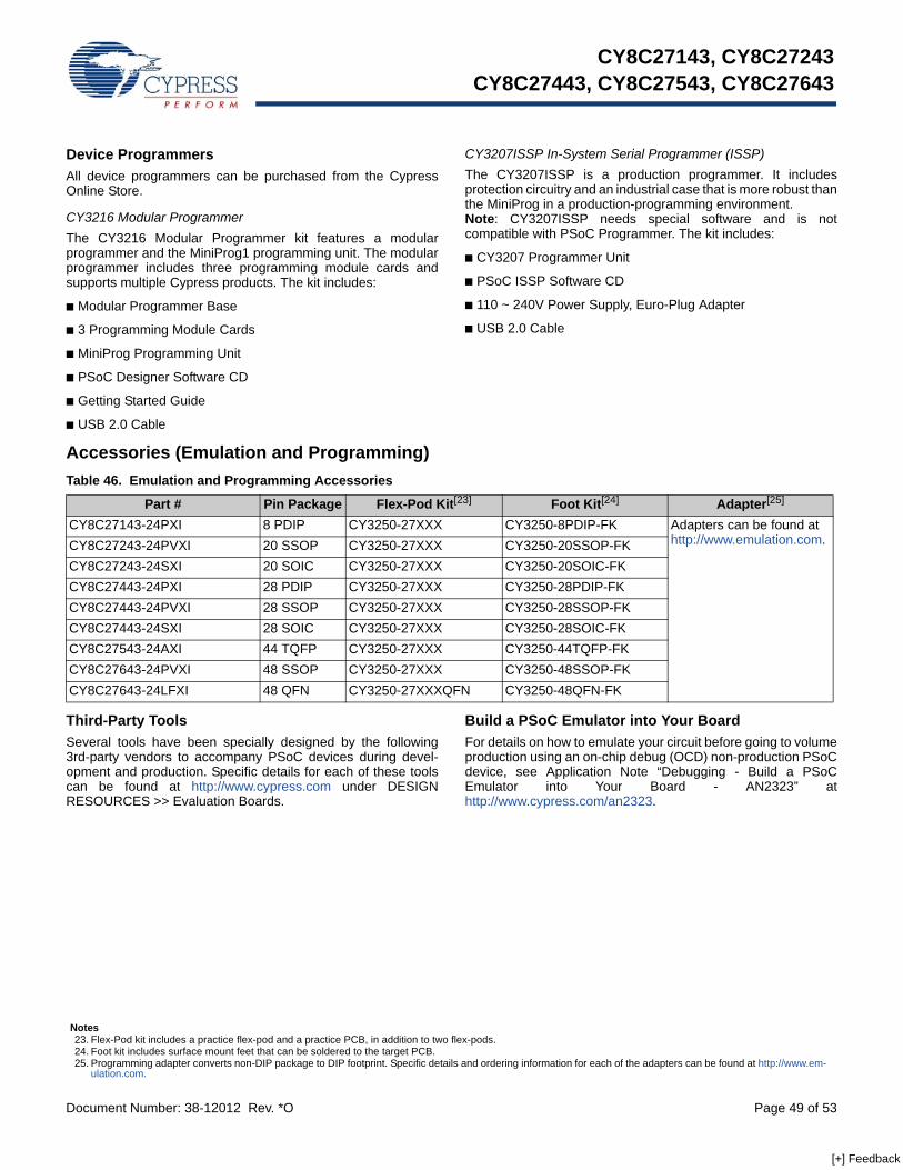
CY8C27143, CY8C27243CY8C27443, CY8C27543, CY8C27643
Document Number: 38-12012 Rev. *O Page 49 of 53
Device ProgrammersAll device programmers can be purchased from the CypressOnline Store.
CY3216 Modular ProgrammerThe CY3216 Modular Programmer kit features a modularprogrammer and the MiniProg1 programming unit. The modularprogrammer includes three programming module cards andsupports multiple Cypress products. The kit includes:
■ Modular Programmer Base
■ 3 Programming Module Cards
■ MiniProg Programming Unit
■ PSoC Designer Software CD
■ Getting Started Guide
■ USB 2.0 Cable
CY3207ISSP In-System Serial Programmer (ISSP)The CY3207ISSP is a production programmer. It includesprotection circuitry and an industrial case that is more robust thanthe MiniProg in a production-programming environment. Note: CY3207ISSP needs special software and is notcompatible with PSoC Programmer. The kit includes:
■ CY3207 Programmer Unit
■ PSoC ISSP Software CD
■ 110 ~ 240V Power Supply, Euro-Plug Adapter
■ USB 2.0 Cable
Accessories (Emulation and Programming)
Third-Party ToolsSeveral tools have been specially designed by the following3rd-party vendors to accompany PSoC devices during devel-opment and production. Specific details for each of these toolscan be found at http://www.cypress.com under DESIGNRESOURCES >> Evaluation Boards.
Build a PSoC Emulator into Your Board For details on how to emulate your circuit before going to volumeproduction using an on-chip debug (OCD) non-production PSoCdevice, see Application Note “Debugging - Build a PSoCEmulator into Your Board - AN2323” athttp://www.cypress.com/an2323.
Table 46. Emulation and Programming Accessories
Part # Pin Package Flex-Pod Kit[23] Foot Kit[24] Adapter[25]
CY8C27143-24PXI 8 PDIP CY3250-27XXX CY3250-8PDIP-FK Adapters can be found at http://www.emulation.com.CY8C27243-24PVXI 20 SSOP CY3250-27XXX CY3250-20SSOP-FK
CY8C27243-24SXI 20 SOIC CY3250-27XXX CY3250-20SOIC-FKCY8C27443-24PXI 28 PDIP CY3250-27XXX CY3250-28PDIP-FKCY8C27443-24PVXI 28 SSOP CY3250-27XXX CY3250-28SSOP-FKCY8C27443-24SXI 28 SOIC CY3250-27XXX CY3250-28SOIC-FKCY8C27543-24AXI 44 TQFP CY3250-27XXX CY3250-44TQFP-FKCY8C27643-24PVXI 48 SSOP CY3250-27XXX CY3250-48SSOP-FKCY8C27643-24LFXI 48 QFN CY3250-27XXXQFN CY3250-48QFN-FK
Notes23. Flex-Pod kit includes a practice flex-pod and a practice PCB, in addition to two flex-pods.24. Foot kit includes surface mount feet that can be soldered to the target PCB.25. Programming adapter converts non-DIP package to DIP footprint. Specific details and ordering information for each of the adapters can be found at http://www.em-
ulation.com.
[+] Feedback

CY8C27143, CY8C27243CY8C27443, CY8C27543, CY8C27643
Document Number: 38-12012 Rev. *O Page 50 of 53
Ordering InformationThe following table lists the CY8C27x43 PSoC device’s key package features and ordering codes.
Table 47. CY8C27x43 PSoC Device Key Features and Ordering Information
Pack
age
Ord
erin
gC
ode
Flas
h(B
ytes
)
RA
M(B
ytes
)
Switc
h M
ode
Pum
p
Tem
pera
ture
Ran
ge
Dig
ital B
lock
s(R
ows
of 4
)
Ana
log
Blo
cks
(Col
umns
of 3
)
Dig
ital I
/OPi
ns
Ana
log
Inpu
ts
Ana
log
Out
puts
XRES
Pin
CY8C27x43 Silicon B – These parts are lead free and offer the following improvements. The DEC_CR1 register selections are enhanced to allow any digital block to be the decimator clock source, the ECO EX and ECO EXW bits in the CPU_SCR1 register are readable, and the accuracy of the analog reference is enhanced (see the Electrical Specifications chapter). All silicon A errata are fixed in silicon B.
8 Pin (300 Mil) DIP CY8C27143-24PXI 16K 256 No -40C to +85C 8 12 6 4 4 No
20 Pin (210 Mil) SSOP CY8C27243-24PVXI 16K 256 Yes -40C to +85C 8 12 16 8 4 Yes
20 Pin (210 Mil) SSOP(Tape and Reel)
CY8C27243-24PVXIT 16K 256 Yes -40C to +85C 8 12 16 8 4 Yes
20 Pin (300 Mil) SOIC CY8C27243-24SXI 16K 256 Yes -40C to +85C 8 12 16 8 4 Yes
20 Pin 300 Mil) SOIC (Tape and Reel)
CY8C27243-24SXIT 16K 256 Yes -40C to +85C 8 12 16 8 4 Yes
28 Pin (300 Mil) DIP CY8C27443-24PXI 16K 256 Yes -40C to +85C 8 12 24 12 4 Yes
28 Pin (210 Mil) SSOP CY8C27443-24PVXI 16K 256 Yes -40C to +85C 8 12 24 12 4 Yes
28 Pin (210 Mil) SSOP (Tape and Reel)
CY8C27443-24PVXIT 16K 256 Yes -40C to +85C 8 12 24 12 4 Yes
28 Pin (300 Mil) SOIC CY8C27443-24SXI 16K 256 Yes -40C to +85C 8 12 24 12 4 Yes
28 Pin (300 Mil) SOIC (Tape and Reel)
CY8C27443-24SXIT 16K 256 Yes -40C to +85C 8 12 24 12 4 Yes
44 Pin TQFP CY8C27543-24AXI 16K 256 Yes -40C to +85C 8 12 40 12 4 Yes
44 Pin TQFP(Tape and Reel)
CY8C27543-24AXIT 16K 256 Yes -40C to +85C 8 12 40 12 4 Yes
48 Pin (300 Mil) SSOP CY8C27643-24PVXI 16K 256 Yes -40C to +85C 8 12 44 12 4 Yes
48 Pin (300 Mil) SSOP (Tape and Reel)
CY8C27643-24PVXIT 16K 256 Yes -40C to +85C 8 12 44 12 4 Yes
48 Pin (7x7) QFN CY8C27643-24LFXI 16K 256 Yes -40C to +85C 8 12 44 12 4 Yes
48 Pin (7x7) QFN(Tape and Reel)
CY8C27643-24LFXIT 16K 256 Yes -40C to +85C 8 12 44 12 4 Yes
48 Pin (7X7X 0.90 MM) QFN (Sawn) CY8C27643-24LTXI 16K 256 Yes -40C to +85C 8 12 44 12 4 Yes
48 Pin (7X7X 0.90 MM) QFN (Sawn) CY8C27643-24LTXIT 16K 256 Yes -40C to +85C 8 12 44 12 4 Yes
56 Pin OCD SSOP CY8C27002-24PVXI[26] 16K 256 Yes -40C to +85C 8 12 44 14 4 Yes
CY8C27x43 Silicon A – Silicon A is not recommended for new designs.
8 Pin (300 Mil) DIP CY8C27143-24PI 16K 256 No -40C to +85C 8 12 6 4 4 No
20 Pin (210 Mil) SSOP CY8C27243-24PVI 16K 256 Yes -40C to +85C 8 12 16 8 4 Yes
20 Pin (210 Mil) SSOP(Tape and Reel)
CY8C27243-24PVIT 16K 256 Yes -40C to +85C 8 12 16 8 4 Yes
20 Pin (300 Mil) SOIC CY8C27243-24SI 16K 256 Yes -40C to +85C 8 12 16 8 4 Yes
20 Pin 300 Mil) SOIC (Tape and Reel)
CY8C27243-24SIT 16K 256 Yes -40C to +85C 8 12 16 8 4 Yes
28 Pin (300 Mil) DIP CY8C27443-24PI 16K 256 Yes -40C to +85C 8 12 24 12 4 Yes
28 Pin (210 Mil) SSOP CY8C27443-24PVI 16K 256 Yes -40C to +85C 8 12 24 12 4 Yes
28 Pin (210 Mil) SSOP (Tape and Reel)
CY8C27443-24PVIT 16K 256 Yes -40C to +85C 8 12 24 12 4 Yes
28 Pin (300 Mil) SOIC CY8C27443-24SI 16K 256 Yes -40C to +85C 8 12 24 12 4 Yes
28 Pin (300 Mil) SOIC (Tape and Reel)
CY8C27443-24SIT 16K 256 Yes -40C to +85C 8 12 24 12 4 Yes
44 Pin TQFP CY8C27543-24AI 16K 256 Yes -40C to +85C 8 12 40 12 4 Yes
Note26. This part may be used for in-circuit debugging. It is NOT available for production.
[+] Feedback
CY8C27143, CY8C27243CY8C27443, CY8C27543, CY8C27643
Document Number: 38-12012 Rev. *O Page 51 of 53
Note For Die sales information, contact a local Cypress sales office or Field Applications Engineer (FAE).
Ordering Code Definitions
44 Pin TQFP(Tape and Reel)
CY8C27543-24AIT 16K 256 Yes -40C to +85C 8 12 40 12 4 Yes
48 Pin (300 Mil) SSOP CY8C27643-24PVI 16K 256 Yes -40C to +85C 8 12 44 12 4 Yes
48 Pin (300 Mil) SSOP (Tape and Reel)
CY8C27643-24PVIT 16K 256 Yes -40C to +85C 8 12 44 12 4 Yes
48 Pin (7x7) MLF CY8C27643-24LFI 16K 256 Yes -40C to +85C 8 12 44 12 4 Yes
48 Pin (7x7) MLF(Tape and Reel)
CY8C27643-24LFIT 16K 256 Yes -40C to +85C 8 12 44 12 4 Yes
48 Pin (7X7X 0.90 MM) QFN (Sawn) CY8C27643-24LTXI 16K 256 Yes -40C to +85C 8 12 44 12 4 Yes
48 Pin (7X7X 0.90 MM) QFN (Sawn) CY8C27643-24LTXIT 16K 256 Yes -40C to +85C 8 12 44 12 4 Yes
Table 47. CY8C27x43 PSoC Device Key Features and Ordering Information (continued)Pa
ckag
e
Ord
erin
gC
ode
Flas
h(B
ytes
)
RA
M(B
ytes
)
Switc
h M
ode
Pum
p
Tem
pera
ture
Ran
ge
Dig
ital B
lock
s(R
ows
of 4
)
Ana
log
Blo
cks
(Col
umns
of 3
)
Dig
ital I
/OPi
ns
Ana
log
Inpu
ts
Ana
log
Out
puts
XRES
Pin
CY 8 C 27 xxx-24xxPackage Type: Thermal Rating:PX = PDIP Pb-Free C = CommercialSX = SOIC Pb-Free I = IndustrialPVX = SSOP Pb-Free E = ExtendedLFX/LKX = QFN Pb-FreeAX = TQFP Pb-FreeSpeed: 24 MHzPart NumberFamily CodeTechnology Code: C = CMOSMarketing Code: 8 = Cypress PSoCCompany ID: CY = Cypress
[+] Feedback

CY8C27143, CY8C27243CY8C27443, CY8C27543, CY8C27643
Document Number: 38-12012 Rev. *O Page 52 of 53
Document History Page
Document Title: CY8C27143, CY8C27243, CY8C27443, CY8C27543, CY8C27643 PSoC® Programmable System-on-ChipDocument Number: 38-12012
Revision ECN No. Submission Date
Origin of Change Description of Change
** 127087 7/01/2003 New Silicon. New document (Revision **).*A 128780 7/29/2003 Engineering and
NWJ.New electrical spec additions, fix of Core Architecture links, corrections to some text, tables, drawings, and format.
*B 128992 8/14/2003 NWJ Interrupt controller table fixed, refinements to Electrical Spec section and Register chapter.
*C 129283 8/28/2003 NWJ Significant changes to the Electrical Specifications section.*D 129442 9/09/2003 NWJ Changes made to Electrical Spec section. Added 20/28-Lead SOIC
packages and pinouts.*E 130129 10/13/2003 NWJ Revised document for Silicon Revision A.*F 130651 10/28/2003 NWJ Refinements to Electrical Specification section and I2C chapter.*G 131298 11/18/2003 NWJ Revisions to GDI, RDI, and Digital Block chapters. Revisions to AC Digital
Block Spec and miscellaneous register changes.*H 229416 See ECN SFV New data sheet format and organization. Reference the PSoC Program-
mable System-on-Chip Technical Reference Manual for additional infor-mation. Title change.
*I 247529 See ECN SFV Added Silicon B information to this data sheet.*J 355555 See ECN HMT Add DS standards, update device table, swap 48-pin SSOP 45 and 46, add
Reflow Peak Temp. table. Add new color and logo. Re-add pinout ISSP notation. Add URL to preferred dimensions for mounting MLF packages. Update Transmitter and Receiver AC Digital Block Electrical Specifications.
*K 523233 See ECN HMT Add Low Power Comparator (LPC) AC/DC electrical spec. tables. Add new Dev. Tool section. Add CY8C20x34 to PSoC Device Characteristics table. Add OCD pinout and package diagram. Add ISSP note to pinout tables. Update package diagram revisions. Update typical and recommended Storage Temperature per industrial specs. Update CY branding and QFN convention. Update copyright and trademarks.
*L 2545030 07/29/2008 YARA Added note to DC Analog Reference Specification table and Ordering Infor-mation.
*M 2696188 04/22/2009 DPT/PYRS Changed title from “ CY8C27143, CY8C27243, CY8C27443, CY8C27543, and CY8C27643 PSoC Mixed Signal Array Final Data Sheet” to “CY8C27143, CY8C27243, CY8C27443, CY8C27543, CY8C27643 PSoC® Programmable System-on-Chip™”. Updated data sheet template. Added 48-Pin QFN (Sawn) package outline diagram and Ordering infor-mation details for CY8C27643-24LTXI and CY8C27643-24LTXIT parts
*N 2762501 09/11/2009 MAXK Updated DC GPIO, AC Chip-Level, and AC Programming Specifications asfollows:Modified TWRITE specification.Replaced TRAMP (time) specification with SRPOWER_UP (slew rate) specifi-cation.Added note [9] to Flash Endurance specification.Added IOH, IOL, DCILO, F32K_U, TPOWERUP, TERASEALL, TPROGRAM_HOT, and TPROGRAM_COLD specifications.
*O 2811860 11/20/2009 ECU Added Contents page. In the Ordering Information table, added 48 Sawn QFN (LTXI) to the Silicon B parts. Updated 28-Pin package drawing (51-85014)
[+] Feedback
Document Number: 38-12012 Rev. *O Revised November 20, 2009 Page 53 of 53
PSoC Designer™ is a trademark and PSoC® is a registered trademark of Cypress Semiconductor Corp. All other trademarks or registered trademarks referenced herein are property of the respectivecorporations. Purchase of I2C components from Cypress or one of its sublicensed Associated Companies conveys a license under the Philips I2C Patent Rights to use these components in an I2Csystem, provided that the system conforms to the I2C Standard Specification as defined by Philips.
CY8C27143, CY8C27243CY8C27443, CY8C27543, CY8C27643
© Cypress Semiconductor Corporation, 2003-2009. The information contained herein is subject to change without notice. Cypress Semiconductor Corporation assumes no responsibility for the useof any circuitry other than circuitry embodied in a Cypress product. Nor does it convey or imply any license under patent or other rights. Cypress products are not warranted nor intended to be usedfor medical, life support, life saving, critical control or safety applications, unless pursuant to an express written agreement with Cypress. Furthermore, Cypress does not authorize its products for useas critical components in life-support systems where a malfunction or failure may reasonably be expected to result in significant injury to the user. The inclusion of Cypress products in life-supportsystems application implies that the manufacturer assumes all risk of such use and in doing so indemnifies Cypress against all charges.
Any Source Code (software and/or firmware) is owned by Cypress Semiconductor Corporation (Cypress) and is protected by and subject to worldwide patent protection (United States and foreign),United States copyright laws and international treaty provisions. Cypress hereby grants to licensee a personal, non-exclusive, non-transferable license to copy, use, modify, create derivative works of,and compile the Cypress Source Code and derivative works for the sole purpose of creating custom software and or firmware in support of licensee product to be used only in conjunction with a Cypressintegrated circuit as specified in the applicable agreement. Any reproduction, modification, translation, compilation, or representation of this Source Code except as specified above is prohibited withoutthe express written permission of Cypress.
Disclaimer: CYPRESS MAKES NO WARRANTY OF ANY KIND, EXPRESS OR IMPLIED, WITH REGARD TO THIS MATERIAL, INCLUDING, BUT NOT LIMITED TO, THE IMPLIED WARRANTIESOF MERCHANTABILITY AND FITNESS FOR A PARTICULAR PURPOSE. Cypress reserves the right to make changes without further notice to the materials described herein. Cypress does notassume any liability arising out of the application or use of any product or circuit described herein. Cypress does not authorize its products for use as critical components in life-support systems wherea malfunction or failure may reasonably be expected to result in significant injury to the user. The inclusion of Cypress’ product in a life-support systems application implies that the manufacturerassumes all risk of such use and in doing so indemnifies Cypress against all charges.
Use may be limited by and subject to the applicable Cypress software license agreement.
Sales, Solutions, and Legal InformationWorldwide Sales and Design SupportCypress maintains a worldwide network of offices, solution centers, manufacturer’s representatives, and distributors. To find the officeclosest to you, visit us at cypress.com/sales.
ProductsPSoC psoc.cypress.comClocks & Buffers clocks.cypress.comWireless wireless.cypress.comMemories memory.cypress.comImage Sensors image.cypress.com
[+] Feedback