pspice a brief primer - hani mehrpouyan circuits/labs pdf/lab 1.pdfjvds 2006 1 pspice a brief primer...
TRANSCRIPT

JVdS 2006 1
PSPICE A brief primer
Contents 1. Introduction 2. Use of PSpice with OrCAD Capture
2.1 Step 1: Creating the circuit in Capture 2.2 Step 2: Specifying the type of analysis and simulation
BIAS or DC analysis DC Sweep simulation
2.3 Step 3: Displaying the simulation Results 2.4 Other types of Analysis:
2.4.1 Transient Analysis 2.4.2 AC Sweep Analysis
3. Additional Circuit Examples with PSpice 3.1Transformer circuit 3.2 AC Sweep of Filter with Ideal Op-amp (Filter circuit) 3.3 AC Sweep of Filter with Real Op-amp (Filter Circuit) 3.4 Rectifier Circuit (peak detector) and the use of a parametric sweep.
Peak Detector simulation Parametric Sweep
3.5 AM Modulated Signal 3.6 Center Tap Transformer
4. Adding and Creating Libraries: Model and Part Symbol files 4.1 Using and Adding Vendor Libraries 4.2 Creating PSpice Symbols from an existing PSpice Model file 4.3 Creating your own PSpice Model file and Symbol Parts
References
1. INTRODUCTION
SPICE is a powerful general purpose analog and mixed-mode circuit simulator that is used to verify circuit designs and to predict the circuit behavior. This is of particular importance for integrated circuits. It was for this reason that SPICE was originally developed at the Electronics Research Laboratory of the University of California, Berkeley (1975), as its name implies:

JVdS 2006 2
Simulation Program for Integrated Circuits Emphasis. PSpice is a PC version of SPICE (which is currently available from OrCAD Corp. of Cadence Design Systems, Inc.). A student version (with limited capabilities) comes with various textbooks. The OrCAD student edition is called PSpice AD Lite. Information about Pspice AD is available from the OrCAD website: http://www.orcad.com/pspicead.aspx
The PSpice Light version has the following limitations: circuits have a maximum of 64 nodes, 10 transistors and 2 operational amplifiers.
SPICE can do several types of circuit analyses. Here are the most important ones:
Non-linear DC analysis: calculates the DC transfer curve. Non-linear transient and Fourier analysis: calculates the voltage and current as a
function of time when a large signal is applied; Fourier analysis gives the frequency spectrum.
Linear AC Analysis: calculates the output as a function of frequency. A bode plot is generated.
Noise analysis Parametric analysis Monte Carlo Analysis
In addition, PSpice has analog and digital libraries of standard components (such as NAND, NOR, flip-flops, MUXes, FPGA, PLDs and many more digital components, ). This makes it a useful tool for a wide range of analog and digital applications.
All analyses can be done at different temperatures. The default temperature is 300K.
The circuit can contain the following components:
Independent and dependent voltage and current sources Resistors Capacitors Inductors Mutual inductors Transmission lines Operational amplifiers Switches Diodes Bipolar transistors MOS transistors JFET MESFET Digital gates and other components (see users manual).

JVdS 2006 3
2. PSpice with OrCAD Capture (release 9.2 Lite edition)
Before one can simulate a circuit one needs to specify the circuit configuration. This can be done in a variety of ways. One way is to enter the circuit description as a text file in terms of the elements, connections, the models of the elements and the type of analysis. This file is called the SPICE input file or source file and has been described somewhere else (see http://www.seas.upenn.edu/%7Ejan/spice/spice.overview.html).
An alternative way is to use a schematic entry program such as OrCAD CAPTURE. OrCAD Capture is bundled with PSpice Lite AD on the same CD that is supplied with the textbook. Capture is a user-friendly program that allows you to capture the schematic of the circuits and to specify the type of simulation. Capture is non only intended to generate the input for PSpice but also for PCD layout design programs.
The following figure summarizes the different steps involved in simulating a circuit with Capture and PSpice. We'll describe each of these briefly through a couple of examples.
Step 1: Circuit Creation with Capture Create a new Analog, mixed AD
project Place circuit parts Connect the parts Specify values and names
Step 2: Specify type of simulation Create a simulation profile Select type of analysis:
o Bias, DC sweep, Transient, AC sweep
Run PSpice
Step 3: View the results
Add traces to the probe window Use cursors to analyze waveforms Check the output file, if needed Save or print the results
Figure 1: Steps involved in simulating a circuit with PSpice. The values of elements can be specified using scaling factors (upper or lower case):
T or Tera (= 1E12); G or Giga (= E9); MEG or Mega (= E6); K or Kilo (= E3); M or Milli (= E-3);
U or Micro (= E-6); N or Nano (= E-9); P or Pico (= E-12) F of Femto (= E-15)
Both upper and lower case letters are allowed in PSpice and HSpice. As an example, one can specify a capacitor of 225 picofarad in the following ways:
225P, 225p, 225pF; 225pFarad; 225E-12; 0.225N

JVdS 2006 4
Notice that Mega is written as MEG, e.g. a 15 megaOhm resistor can be specified as 15MEG, 15MEGohm, 15meg, or 15E6. Be careful not to use M for Mega! When you write 15Mohm or 15M, Spice will read this as 15 milliOhm!
We'll illustrate the different types of simulations for the following circuit:
Figure 2: Circuit to be simulated (screen shot from OrCAD Capture).
2.1 Step 1: Creating the circuit in Capture
2.1.1 Create new project:
1. Open OrCAD Capture 2. Create a new Project: FILE MENU/NEW_PROJECT 3. Enter the name of the project 4. Select Analog or Mixed-AD 5. When the Create PSpice Project box opens, select "Create Blank Project".
A new page will open in the Project Design Manager as shown below.

JVdS 2006 5
Figure 3: Design manager with schematic window and toolbars (OrCAD screen capture) 2.1.2. Place the components and connect the parts
1. Click on the Schematic window in Capture. 2. To Place a part go to PLACE/PART menu or click on the Place Part Icon. This will open
a dialog box shown below.
Figure 4: Place Part window
3. Select the library that contains the required components. Type the beginning of the name in the Part box. The part list will scroll to the components whose name contains the same letters. If the library is not available, you need to add the library, by clicking on the Add Library button. This will bring up the Add Library window. Select the desired library. For Spice you should select the libraries from the Capture/Library/PSpice folder.
Analog: contains the passive components (R,L,C), mutual inductane, transmission line, and voltage and current dependent sources (voltage dependent voltage source E, current- dependent current source F, voltage-dependent current source G and current-dependent voltage source H). Source: give the different type of independent voltage and current sources, such as Vdc, Idc, Vac, Iac, Vsin, Vexp, pulse, piecewise linear, etc. Browse the library to see what is available. Eval: provides diodes (D…), bipolar transistors (Q…), MOS transistors, JFETs (J…), real opamp such as the u741, switches (SW_tClose, SW_tOpen), various digital gates and components. Abm: contains a selection of interesting mathematical operators that can be applied to signals, such as multiplication (MULT), summation (SUM), Square Root (SWRT), Laplace (LAPLACE), arctan (ARCTAN), and many more. Special: contains a variety of other components, such as PARAM, NODESET, etc.

JVdS 2006 6
4. Place the resistors, capacitor (from the Analog library), and the DC voltage and current source. You can place the part by the left mouse click. You can rotate the components by clicking on the R key. To place another instance of the same part, click the left mouse button again. Hit the ESC key when done with a particular element. You can add initial conditions to the capacitor. Double-click on the part; this will open the Property window that looks like a spreadsheet. Under the column, labeled IC, enter the value of the initial condition, e.g. 2V. For our example we assume that IC was 0V (this is the default value).
5. After placing all part, you need to place the Ground terminal by clicking on the GND icon (on the right side toolbar – see Fig. 3). When the Place Ground window opens, select GND/CAPSYM and give it the name 0 (i.e. zero). Do not forget to change the name to 0, otherwise PSpice will give an error or "Floating Node". The reason is that SPICE needs a ground terminal as the reference node that has the node number or name 0 (zero).
Figure 5: Place the ground terminal box; the ground terminal should have the name 0
6. Now connect the elements using the Place Wire command from the menu (PLACE/WIRE) or by clicking on the Place Wire icon.
7. You can assign names to nets or nodes using the Place Net Alias command (PLACE/NET ALIAS menu). We will do this for the output node and input node. Name these Out and In, as shown in Figure 2.
2.1.3. Assign Values and Names to the parts
1. Change the values of the resistors by double-clicking on the number next to the resistor.
You can also change the name of the resistor. Do the same for the capacitor and voltage and current source.
2. If you haven't done so yet, you can assign names to nodes (e.g. Out and In nodes). 3. Save the project

JVdS 2006 7
2.1.4. Netlist The netlist gives the list of all elements using the simple format:
R_name node1 node2 value C_name nodex nodey value, etc.
1. You can generate the netlist by going to the PSPICE/CREATE NETLIST menu. 2. Look at the netlist by double clicking on the Output/name.net file in the Project Manager
Window (in the left side File window).
Note on Current Directions in elements: The positive current direction in an element such as a resistor is from node 1 to node 2. Node 1 is either the left pin or the top pin for an horizontal or vertical positioned element (.e.g a resistor). By rotating the element 180 degrees one can switch the pin numbers. To verify the node numbers you can look at the netlist:
e.g. R_R2 node1 node2 10ke.g. R_R2 0 OUT 10k
Since we are interested in the current direction from the OUT node to the ground, we need to rotate the resistor R2 twice so that the node numbers are interchanged:
R_R2 OUT 0 10k
2.2 Step 2: Specifying the type of analysis and simulation
As mentioned in the introduction, Spice allows you do to a DC bias, DC Sweep, Transient with Fourier analysis, AC analysis, Montecarlo/worst case sweep, Parameter sweep and Temperature sweep. We will first explain how to do the Bias and DC Sweep on the circuit of Figure 2.
2.2.1 BIAS or DC analysis
1. With the schematic open, go to the PSPICE menu and choose NEW SIMULATION
PROFILE. 2. In the Name text box, type a descriptive name, e.g. Bias 3. From the Inherit From List: select none and click Create. 4. When the Simulation Setting window opens, for the Analyis Type, choose Bias Point
and click OK. 5. Now you are ready to run the simulation: PSPICE/RUN 6. A window will open, letting you know if the simulation was successful. If there are
errors, consult the Simulation Output file. 7. To see the result of the DC bias point simulation, you can open the Simulation Output
file or go back to the schematic and click on the V icon (Enable Bias Voltage Display) and I icon (current display) to show the voltage and currents (see Figure 6).

JVdS 2006 8
The check the direction of the current, you need to look at the netlist: the current is positive flowing from node1 to node1 (see note on Current Direction above).
Figure 6: Results of the Bias simulation displayed on the schematic. 2.2.2 DC Sweep simulation
We will be using the same circuit but will evaluate the effect of sweeping the voltage source between 0 and 20V. We'll keep the current source constant at 1mA.
1. Create a new New Simulation Profile (from the PSpice Menu); We'll call it DC Sweep 2. For analysis select DC Sweep; enter the name of the voltage source to be swept: V1. The
start and end values and the step need to be specified: 0, 20 and 0.1V, respectively (see Fig. below).
Figure 7: Setting for the DC Sweep simulation.
3. Run the simulation. PSpice will generate an output file that contains the values of all voltages and currents in the circuit.

JVdS 2006 9
2.3 Step 3: Displaying the simulation Results PSpice has a user-friendly interface to show the results of the simulations. Once the simulation is finished a Probe window will open.
Figure 8: Probe window
1. From the TRACE menu select ADD TRACE and select the voltages and current you like
to display. In our case we'll add V(out) and V(in). Click OK.
Figure 9: Add Traces window

JVdS 2006 10
2. You can also add traces using the "Voltage Markers" in the schematic. From the PSPICE menu select MARKERS/VOLTAGE LEVELS. Place the makers on the Out and In node. When done, right click and select End Mode.
Figure 10: Using Voltage Markers to show the simulation result of V(out) and V(in)
3. Go to back to PSpice. You will notice that the waveforms will appear. 4. You can add a second Y Axis and use this to display e.g. the current in Resistor R2, as
shown below. Go to PLOT/Add Y Axis. Next, add the trace for I(R2). You may need to flip (rotate twice) the resistor R2 and adjust the y scale.
5. You can also use the cursors on the graphs for Vout and Vin to display the actual values at certain points. Go to TRACE/CURSORS/DISPLAY
6. The cursors will be associated with the first trace, as indicated by the small small rectangle around the legend for V(out) at the bottom of the window. Left click on the first trace. The value of the x and y axes are displayed in the Probe window. When you right click on V(out) the value of the second cursor will be given together with the difference between the first and second cursor.
7. To place the second cursor on the second trace (for V(in)), right click the legend for V(in). You'll notice the outline around V(in) at the bottom of the window. When you right click the second trace the cursor will snap to it. The values of the first and second cursor will be shown in Probe window.
8. You can chance the X and Y axes by double clicking on them. 9. When adding traces you can perform mathematical calculations on the traces, as
indicated in the Add Trace Window to the right of Figure 9.

JVdS 2006 11
Figure 11: Result of the DC sweep, showing Vout, Vin and the current through resistor R2. Cursors were used for V(out) and V(in).
2.4 Other types of Analysis
2.4.1 Transient Analysis
We'll be using the same circuit as for the DC sweep, except that we'll apply the voltage and current sources by closing a switch, as shown in Figure 12.
Figure 12: Circuit used for the transient simulation.
1. Insert the SW_TCLOSE switch from the EVAL Library as shown above. Double click on
the switch TCLOSE value and enter the value when the switch closes. Lets make TCLOSE = 5ms.
2. Set up the Transient Analysis: go to the PSPICE/NEW SIMULATION PROFILE. 3. Give it a name (e.g. Transient). When the Simulation Settings window opens, select
"Time Domain (Transient)" Analysis. Enter also the Run Time. Lets make it 50ms. For the Max Step size, you can leave it blank or enter 10us.
4. Run PSpice. 5. A Probe window in PSpice will open. You can now add the traces to display the results.
In the figure below we plotted the current through the capacitor in the top window and the voltage over the capacitor on the bottom one. You may need to flip (rotate twice) the capacitor to get the graph on the top window. We use the cursor to find the time constant of the exponential waveform (by finding the 0.632 x V(out)max = 9.48. The

JVdS 2006 12
cursor gave a corresponding time of 30ms which gives a time constant of 30-5=25ms (5 ms is subtracted because the switch closed at 5ms). To get the graph in Figure 13, change the Run Time to 200ms.
Figure 13: Results of the transient simulation of Figure 12.
6. Instead of using a switch we can also use a voltage source that changes over time. This was done in Figure 14 where we used the VPULSE and IPULSE sources from the SOURCE Library. We entered the voltage levels (V1 and V2), the delay (TD), Rise and Fall Times, Pulse Width (PW) and the Period (PER). The values are indicated in the figure below. For details on these parameters click here. A description of other Spice elements can be found in the User’s guide or in the Spice Tutorial. (http://www.seas.upenn.edu/~jan/spice/)
Figure 14: Circuit with a PULSE voltage and current source.
7. After doing the transient simulation results can be displayed as was done before. The
amplitude of V(out) and I(C1) may be different than with using a switch. 8. The last example of a transient analysis is with a sinusoidal signal VSIN. The circuit is
shown below. We made the amplitude 10V and frequency 10 Hz.

JVdS 2006 13
Figure 15: Circuit with a sinusoidal input.
9. Create a Simulation Profiler for the transient analysis and run PSpice. Use an end time of
600ms. 10. The result of the simulation for Vout and Vin are given in the figure below.
Figure 16: Transient simulation with a sinusoidal input. 2.4.2 AC Sweep Analysis
The AC analysis will apply a sinusoidal voltage whose frequency is swept over a specified range. The simulation calculates the corresponding voltage and current amplitude and phases for each frequency. When the input amplitude is set to 1V, then the output voltage is basically the transfer function. In contrast to a sinusoidal transient analysis, the AC analysis is not a time domain simulation but rather a simulation of the sinusoidal steady state of the circuit. When the circuit contains non-linear element such as diodes and transistors, the elements will be replaced their small-signal models with the parameter values calculated according to the corresponding biasing point.
In the first example, we'll show a simple RC filter corresponding to the circuit of Figure 17.

JVdS 2006 14
Figure 17: Circuit for the AC sweep simulation.
1. Create a new project and build the circuit 2. For the voltage source use VAC from the Sources library. 3. Make the amplitude of the input source 1V. 4. Create a Simulation Profile. In the Simulation Settings window, select AC Sweep/Noise. 5. Enter the start and end frequencies and the number of points per decade. For our example
we use 0.1Hz, 10 kHz and 11, respectively. 6. Run the simulation 7. In the Probe window, add the traces for the input voltage. We added a second window to
display the phase in addition to the magnitude of the output voltage. The voltage can be displayed in dB by specifying Vdb(out) in the Add Trace window (type Vdb(out) in the Trace Expression box. For the phase, type VP(out).
8. An alternative to show the voltage in dB and phase is to use markers on the schematics: PSPICE/MARKERS/ADVANCED/dBMagnitude or Phase of Voltage, or current. Place the markers on the node of interest.
9. We used the cursors in Figure 18 to find the 3dB point. The value is 6.49 Hz corresponding to a time constant of 25 ms (R1||R2.C). At 10 Hz the attenuation of Vout is 11.4db or a factor of 3.72. This corresponds to the value of the amplitude of the output voltage obtained during the transient analysis of Figure 16 above.

JVdS 2006 15
3. Additional Circuit Examples with PSpice
3.1 Transformer circuit
SPICE has no model for an ideal transformer. An ideal transformer is simulated using mutual inductances such that the transformer ratio N1/N2 = sqrt(L1/L2). The part in PSpice is called XFRM_LINEAR (in the Analog Library). Make the coupling factor K close to or equal to one (ex. K=1) and choose L such that wL >> the resistance seen be the inductor. The secondary circuit needs a DC connection to ground. This can be accomplished by adding a large resistor to ground or giving the primary and secondary circuits a common node. The following example illustrates how to simulate a transformer.
Figure 3.1.1: Circuit with ideal transformer
To get the name and value of the transformer, double click on the transformer. Then, highlight L1_VALUE and L2_VALUE. Click Display. Change to “Name and Value”. For the above example, lets make wL2 >> 500 Ohm or L2> 500/(60*2pi) ; lets make L2 at least 10 times larger, ex. L2=20H. L1 can than be found from the turn ratio: L1/L2 = (N1/N2)^2. For a turn ratio of 10 this makes L1=L2x100=2000H. The circuit as entered in PSpice Capture is shown in Figure 3.1.2 and the result in Figure 3.1.3
Figure 3.1.2: Circuit with ideal transformer as entered in PSpice Capture (the transformer TX is modeled by the part XFRM_LINEAR of the Analog Library).
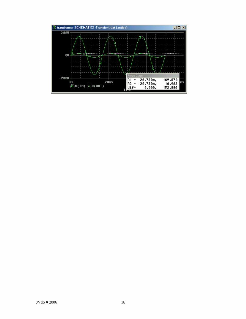
JVdS 2006 16

JVdS 2006 17
Figure 3.1.3: Results of the transient simulation of the above circuit.
3.2 AC Sweep of Filter with Ideal Op-amp (Filter circuit)
The following circuit will be simulated with PSpice.
Figure 3.2.1: Active Filter Circuit with ideal op-amp.
Use “OPAMP” from Analog library. We have used off-page connectors (OFFPAGELEFT-R from the CAPSYM library; or by clicking on the off-page icon) for the input and outputs. The name of the connectors can be changed by double-clicking on the name of the off-page connector. By giving the same name to two connectors (or nodes), the two nodes will be connected (no wires are needed). For te voltage source we used the VAC from the SOURCE Library. We gave it an amplitude of 1V so that the output voltage will correspond to the amplification (or transfer function) of the filter. In the Simulation Analysis, select AC Sweep, and enter the starting (10mHz), ending frequency (10kHz), and the number of points per decade (11).
The result is given in the figure below. The magnitude is given on the left Y axis while the phase is given by the right Y axis. The cursors have been used to find the 3db points of the bandpass filters, corresponding to 0.63 Hz and 32 Hz for the low and high breakpoints, respectively. These numbers correspond to the values of the time constants given in Fig. 3.2.1. The phase at these points is -135 and -224 degrees.

JVdS 2006 18
Figure 3.2.2: Results of the AC sweep of the Active Filter Circuit of the figure above. 3.3 AC Sweep of Filter with Real Op-amp (Filter circuit)
The circuit with a real op-amp is shown below. We selected the “uA741” op-amp to build the filter. The simulation results are shown in Figure 3.3.2. As one would expect the differences between the filter with the real and ideal op-amps are minimal in this frequency range.
Figure 3.3.1: Active Filter Circuit with the U741 Op-amp.

JVdS 2006 19
Figure 3.3.2: Results of the AC sweep of the Active Filter Circuit with real Op-amp (U741) of the figure above.
3.4 Rectifier Circuit (peak detector) and the use of a parametric sweep.
3.4.1: Peak Detector simulation
Figure 3.4.1: Rectifier circuit with the D1N4148 diode and a load resistor of 500 Ohm.
The results of the simulation are given in Fig. 3.4.2. The ripple has a peak-to-peak value of 777mV as indicated by the cursors. The maximum output voltage is 13.997V which is one volt below the input of 15V.

JVdS 2006 20
Figure 3.4.2: Simulation results of the rectifier circuit.
3.4.2 Parametric Sweep
It is interesting to see the effect of the load resistance on the output voltage and its ripple voltage. This can be done using the PARAM part.
Figure 3.4.3: Circuit used for the parametric sweep of the load resistor.
a. Adding the Parameter Part
a. Double click on the value (500 Ohms) of the load resistor R1 to {RLval}. Use curly brackets. PSpice interprets the text between curly brackets as an expression that it evaluate to a numerical expression. Click OK when done.
b. Add the PARAM part to the circuit. You'll find this part in the SPECIAL library. c. Double click on the PARAM part. This will open a spreadsheet like window
showing the PARAM definition. You will need to add a new column to this spread sheet. Click on NEW COLUMN and enter for Property Name, RLval (without the curly brackets).
d. You will notice that the new column RLval has been created. Below the RLval enter the initial value for the resistor: lets make it 500, as shown in Figure 3.4.4 below.

JVdS 2006 20
Figure 3.4.4: Property Editor window for the PARAM part, showing the newly created RLval column.
e. While the cell in which you entered the value 500 still selected click the
DISPLAY button. You can now specify what to display: select Name and Value. Click OK.
f. Click the APPLY button before closing the Property editor. g. Save the design.
b. Create the Simulation Profile for the Parametric Analysis
a. Select PSPICE/NEW_SIMULATION_PROFILE b. Type in the name of the profile, e.g. Parametric c. In the Simulation Setting window, select Analysis Tab if the window does not
open. d. For the Analysis type select Transient (or the type of analysis you intend to
perform; in this example we'll do a transient analysis) e. Under Option, slect Parametric sweep as shown in Figure 3.4.5. f. For the Sweep Variable, select Global Parameter and enter the Parameter name:
RLval. Under sweep type give the start, end and increment for the parameter. We'll used 250, 1kOhm and 250, respectively (see Figure 3.4.5).
g. Click OK
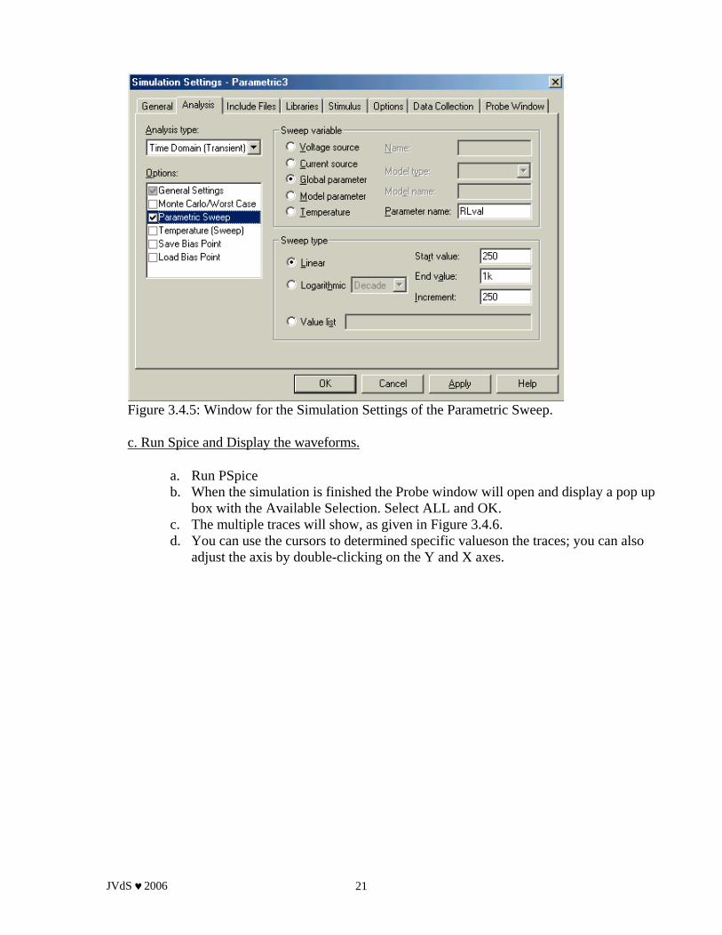
JVdS 2006 21
Figure 3.4.5: Window for the Simulation Settings of the Parametric Sweep.
c. Run Spice and Display the waveforms.
a. Run PSpice b. When the simulation is finished the Probe window will open and display a pop up
box with the Available Selection. Select ALL and OK. c. The multiple traces will show, as given in Figure 3.4.6. d. You can use the cursors to determined specific valueson the traces; you can also
adjust the axis by double-clicking on the Y and X axes.

JVdS 2006 22
Figure 3.4.6: Results of the parametric sweep of the load resistor, varying from 250 to 1000 Ohm in steps of 250 Ohm.
3.5 AM Modulated Signal (AM Modulation)
An Amplitude modulated (AM) signal has the expression,
vam(t) = [(A + Vm cos(2fmt)] cos(2fct) = A[1 + m cos(2fmt)] cos(2fct)
in which a sinusoidal high frequency carrier waveform cos(2fct) is modulated by a sinusoidal modulating of frequency fm. The modulating frequency can be any signal. For this example we’ll assume it is a sinusoid. The modulation index is called m.
To generate a AM signal in PSpice we can make use of the Multiplication function MULT that can be found in the ABM library. Figure 3.51 shows the schematic that generates the AM signal over the resistor R1.
Figure 3.5.1: Schematic for the generation of an AM signal

JVdS 2006 23
The result of a transient simulation is shown in the figure below. One can also look at the Fourier of the simulated output signal. In the Probe window click on the FFT icon, located on the top toolbar, or go to the PSPICE/FOURIER menu. The Fourier spectrum of the displayed trace will be shown. You can change the X axis by double-clicking on it. Figure 3.5.3 gives the Fourier spectrum with the main peak corresponding to the carrier frequency of 5kHz and two side peaks at 4.5 and 5.5 kHz, indicating that the modulating frequency is 500Hz. You can use the cursors to get accurate readings.
Figure 3.5.2: Simulated waveform (transient analysis) of the circuit above, with (A=1V, fm=500 Hz, fc=5kHz and m=0.5)
Figure 3.5.3: Fourier spectrum of the waveform of Figure 3.5.2.

JVdS 2006 24
3.6. Center Tap Transformer
There is no direct model in PSpice for a center tap transformer. However, one can use mutually coupled inductors to simulate a center tap transformer. Figure 3.6.1 shows the schematic of the circuit. We used one primary inductor L1 and two secondary inductors L1 and L2 put in series. In addition we added a K-Linear element.
Figure 3.6.1: Circuit with Center Tap Transformer with a ratio of 10:1.
After placing the element on the schematic give each element its value. Use for the input voltage a sinusoid with amplitude of 100 V and frequency 60 Hz. Notice that we added a small resistor R1 in series with the voltage source and the inductor. This was needed to prevent a short circuit in DC (Spice would give en error without this resistor). We have kept it small equal to 1 Ohm. Assume that we want to have a step-down transformer with a ratio of 10:1 to each secondary output. The ratios of the inductors L2/L1 and L3/L1 must then be equal to 1/102 (or =sqrt(L2/L1)=0.1). We made L1=1000 and L2-L3=10H.
Double-click on the K-Linear element and type under the column headings for L1, L2, L3, the values LP, Ls1, Ls2. When done, click the APPLY button and close the properties window.
Go to PSpice/CREATE_NETLIST to generate the netlist. To see the list, go to the Project Manager and double-click on OUTPUTs: name.net file. The netlist looks as follows:
* source CENTERTAPTRANSFOR2 Kn_K1 L_Lp L_Ls1 L_Ls2 1 L_Lp 0 N00241 1000 L_Ls1 0 VO1 10 L_Ls2 VO2 0 10 V_V1 N00203 0 +SIN 0V 100V 60 0 0 0 R_R1 N00203 N00241 1k R_R2 0 VO1 1k R_R3 VO2 0 1k
Create a new Simulation Profile (Transient) with " Time to run = 50ms". The result is shown in Figure 3.6.2. Notice that the max output is 10V as one would expect from a transformer ratio of 10:1 with an input voltage of 100Vmax.. The two outputs are 180 degrees out of phase.

JVdS 2006 25
Figure 3.6.2: Output of the circuit of Fig. 3.6.1.
References
1. OrCAD website for PSpice (http://www.orcad.com/pspicead.aspx), has application notes, download, examples and interesting links.
2. OrCAD website for CAPTURE. (http://www.orcad.com/orcadcapture.aspx) 3. PSpice User’s manual, OrCAD Corp. (Cadence Design Systems, Inc.) 4. PSpice Reference Guide, OrCAD Corp. (Cadence Design Systems, Inc.) 5. PSpice Library Guide, OrCAD Capture User's Guide, (Cadence Design Systems, Inc.) 6. OrCAD Capture User’s Guide, OrCAD Corp., (Cadence Design Systems, Inc.) 7. SPICE Tutorial, http://www.seas.upenn.edu/~jan/spice/ 8. A. Vladimirescu, “The Spice Book,” J. Wiley & Sons, New York, 1994. 9. B. Carter, "Using Texas Instruments Spice Models in PSpice, Application Report,
SLOA070, Texas Instruments, Dallas, TX, September 2001.

JVdS 2006 30
10. A. Sedra and K. C. Smith, "Microelectronic Circuits," Oxford University Press, 2004, with accompanying Rom CD containing Spice Circuit Examples.
Jan Van der Spiegel, ©2006 jan_at_seas.upenn.edu Updated March 19, 2006