pspice for circuit theory and electronic...
TRANSCRIPT
MOBK059-FM MOBKXXX-Sample.cls March 9, 2007 10:43
PSpice for Circuit Theory andElectronic Devices

MOBK059-FM MOBKXXX-Sample.cls March 12, 2007 13:41
Copyright © 2007 by Morgan & Claypool
All rights reserved. No part of this publication may be reproduced, stored in a retrieval system, or transmitted in
any form or by any means—electronic, mechanical, photocopy, recording, or any other except for brief quotations
in printed reviews, without the prior permission of the publisher.
PSpice for Circuit Theory and Electronic Devices
Paul Tobin
www.morganclaypool.com
ISBN: 1598291564 paperback
ISBN: 9781598291568 paperback
ISBN: 1598291572 ebook
ISBN: 9781598291575 ebook
DOI: 10.2200/S00068ED1V01Y200611DCS007
A Publication in the Morgan & Claypool Publishers series
SYNTHESIS LECTURES ON DIGITAL CIRCUITS AND SYSTEMS #7
Lecture #7
Series Editor: Mitchell A. Thornton, Southern Methodist University
Library of Congress Cataloging-in-Publication Data
Series ISSN: 1932-3166 print
Series ISSN: 1932-3174 electronic
First Edition
10 9 8 7 6 5 4 3 2 1

MOBK059-FM MOBKXXX-Sample.cls March 12, 2007 13:41
PSpice for Circuit Theory andElectronic Devices
Paul TobinSchool of Electronic and Communications Engineering
Dublin Institute of Technology
Ireland
SYNTHESIS LECTURES ON DIGITAL CIRCUITS AND SYSTEMS #7
M&C
M o r g a n & C l a y p o o l P u b l i s h e r s
MOBK059-FM MOBKXXX-Sample.cls March 9, 2007 10:43
iv
ABSTRACTPSpice for Circuit Theory and Electronic Devices is one of a series of five PSpice books and
introduces the latest Cadence Orcad PSpice version 10.5 by simulating a range of DC and AC
exercises. It is aimed primarily at those wishing to get up to speed with this version but will be of
use to high school students, undergraduate students, and of course, lecturers. Circuit theorems
are applied to a range of circuits and the calculations by hand after analysis are then compared
to the simulated results. The Laplace transform and the s-plane are used to analyze CR and
LR circuits where transient signals are involved. Here, the Probe output graphs demonstrate
what a great learning tool PSpice is by providing the reader with a visual verification of
any theoretical calculations. Series and parallel-tuned resonant circuits are investigated where
the difficult concepts of dynamic impedance and selectivity are best understood by sweeping
different circuit parameters through a range of values.
Obtaining semiconductor device characteristics as a laboratory exercise has fallen out
of favour of late, but nevertheless, is still a useful exercise for understanding or modelling
semiconductor devices. Inverting and non-inverting operational amplifiers characteristics such
as gain-bandwidth are investigated and we will see the dependency of bandwidth on the gain
using the performance analysis facility. Power amplifiers are examined where PSpice/Probe
demonstrates very nicely the problems of cross-over distortion and other problems associated
with power transistors. We examine power supplies and the problems of regulation, ground
bounce, and power factor correction. Lastly, we look at MOSFET device characteristics and
show how these devices are used to form basic CMOS logic gates such as NAND and NOR
gates.
KEYWORDSCadence Orcad PSpice V10.5, Ohm’s law, Kirchhoff’s laws, Thevenin and Norton theorems,
Mesh and nodal analysis, Laplace, transients, transfer functions, resonance, transformers, power
supplies, ground bounce, operational amplifiers, power amplifiers.

MOBK059-FM MOBKXXX-Sample.cls March 9, 2007 10:43
I would like to dedicate this book to my wife and friend,Marie and sons Lee, Roy, Scott and Keith and my
parents (Eddie and Roseanne), sisters, Sylvia,Madeleine, Jean, and brother, Ted.

MOBK059-FM MOBKXXX-Sample.cls March 9, 2007 10:43
MOBK059-FM MOBKXXX-Sample.cls March 9, 2007 10:43
vii
Contents
Preface . . . . . . . . . . . . . . . . . . . . . . . . . . . . . . . . . . . . . . . . . . . . . . . . . . . . . . . . . . . . . . . . . . . . . . xiii
1. Introduction to PSpice and Ohm’s Law . . . . . . . . . . . . . . . . . . . . . . . . . . . . . . . . . . . . . . . . . 1
1.1 Laying out A Schematic . . . . . . . . . . . . . . . . . . . . . . . . . . . . . . . . . . . . . . . . . . . . . . . . . . 1
1.2 Libraries . . . . . . . . . . . . . . . . . . . . . . . . . . . . . . . . . . . . . . . . . . . . . . . . . . . . . . . . . . . . . . . . .2
1.2.1 Moving Components Around . . . . . . . . . . . . . . . . . . . . . . . . . . . . . . . . . . . . . . 4
1.2.2 Display Properties . . . . . . . . . . . . . . . . . . . . . . . . . . . . . . . . . . . . . . . . . . . . . . . . 5
1.3 The DC Circuit . . . . . . . . . . . . . . . . . . . . . . . . . . . . . . . . . . . . . . . . . . . . . . . . . . . . . . . . . 6
1.3.1 New Simulation . . . . . . . . . . . . . . . . . . . . . . . . . . . . . . . . . . . . . . . . . . . . . . . . . . 7
1.3.2 Main Operational Icons . . . . . . . . . . . . . . . . . . . . . . . . . . . . . . . . . . . . . . . . . . . 8
1.3.3 Simulation Settings . . . . . . . . . . . . . . . . . . . . . . . . . . . . . . . . . . . . . . . . . . . . . . . 9
1.4 Potential Divider . . . . . . . . . . . . . . . . . . . . . . . . . . . . . . . . . . . . . . . . . . . . . . . . . . . . . . . . 9
1.4.1 Current Divider . . . . . . . . . . . . . . . . . . . . . . . . . . . . . . . . . . . . . . . . . . . . . . . . . 11
1.5 Exercises . . . . . . . . . . . . . . . . . . . . . . . . . . . . . . . . . . . . . . . . . . . . . . . . . . . . . . . . . . . . . . . 12
2. The DC Circuit and Kirchhoff’s Laws . . . . . . . . . . . . . . . . . . . . . . . . . . . . . . . . . . . . . . . . . 13
2.1 Maximum Power Transfer . . . . . . . . . . . . . . . . . . . . . . . . . . . . . . . . . . . . . . . . . . . . . . . 13
2.1.1 Param Part . . . . . . . . . . . . . . . . . . . . . . . . . . . . . . . . . . . . . . . . . . . . . . . . . . . . . . 13
2.1.2 Simulation Settings . . . . . . . . . . . . . . . . . . . . . . . . . . . . . . . . . . . . . . . . . . . . . . 13
2.1.3 Trace Expression Box . . . . . . . . . . . . . . . . . . . . . . . . . . . . . . . . . . . . . . . . . . . . 15
2.2 Changing the X-Axis Variable . . . . . . . . . . . . . . . . . . . . . . . . . . . . . . . . . . . . . . . . . . . 16
2.2.1 The Log Command . . . . . . . . . . . . . . . . . . . . . . . . . . . . . . . . . . . . . . . . . . . . . . 17
2.3 Mesh Analysis . . . . . . . . . . . . . . . . . . . . . . . . . . . . . . . . . . . . . . . . . . . . . . . . . . . . . . . . . . 17
2.4 Nodal Analysis . . . . . . . . . . . . . . . . . . . . . . . . . . . . . . . . . . . . . . . . . . . . . . . . . . . . . . . . . . 20
2.5 Exercises . . . . . . . . . . . . . . . . . . . . . . . . . . . . . . . . . . . . . . . . . . . . . . . . . . . . . . . . . . . . . . . 22
3. Transient Circuits and Laplace Transforms . . . . . . . . . . . . . . . . . . . . . . . . . . . . . . . . . . . . 23
3.1 Transient Analysis . . . . . . . . . . . . . . . . . . . . . . . . . . . . . . . . . . . . . . . . . . . . . . . . . . . . . . 23
3.2 Laplace Transform and Capacitance . . . . . . . . . . . . . . . . . . . . . . . . . . . . . . . . . . . . . . 23
3.3 Inductance . . . . . . . . . . . . . . . . . . . . . . . . . . . . . . . . . . . . . . . . . . . . . . . . . . . . . . . . . . . . . 24
3.4 First-Order CR and LR Circuits . . . . . . . . . . . . . . . . . . . . . . . . . . . . . . . . . . . . . . . . . .24
3.4.1 Solution . . . . . . . . . . . . . . . . . . . . . . . . . . . . . . . . . . . . . . . . . . . . . . . . . . . . . . . . 25
3.4.2 Partial Fraction Expansion . . . . . . . . . . . . . . . . . . . . . . . . . . . . . . . . . . . . . . . . 26

MOBK059-FM MOBKXXX-Sample.cls March 9, 2007 10:43
viii PSPICE FOR CIRCUIT THEORY AND ELECTRONIC DEVICES
3.4.3 Initial Conditions . . . . . . . . . . . . . . . . . . . . . . . . . . . . . . . . . . . . . . . . . . . . . . . . 27
3.5 Example 2 . . . . . . . . . . . . . . . . . . . . . . . . . . . . . . . . . . . . . . . . . . . . . . . . . . . . . . . . . . . . . . 28
3.5.1 Solution . . . . . . . . . . . . . . . . . . . . . . . . . . . . . . . . . . . . . . . . . . . . . . . . . . . . . . . . 28
3.6 Example 3 . . . . . . . . . . . . . . . . . . . . . . . . . . . . . . . . . . . . . . . . . . . . . . . . . . . . . . . . . . . . . . 29
3.6.1 Solution . . . . . . . . . . . . . . . . . . . . . . . . . . . . . . . . . . . . . . . . . . . . . . . . . . . . . . . . 30
3.7 Example 4 . . . . . . . . . . . . . . . . . . . . . . . . . . . . . . . . . . . . . . . . . . . . . . . . . . . . . . . . . . . . . . 32
3.7.1 Solution . . . . . . . . . . . . . . . . . . . . . . . . . . . . . . . . . . . . . . . . . . . . . . . . . . . . . . . . 33
3.8 Exercise . . . . . . . . . . . . . . . . . . . . . . . . . . . . . . . . . . . . . . . . . . . . . . . . . . . . . . . . . . . . . . . . 34
4. Transfer Functions and System Parameters . . . . . . . . . . . . . . . . . . . . . . . . . . . . . . . . . . . . 35
4.1 Transfer Functions . . . . . . . . . . . . . . . . . . . . . . . . . . . . . . . . . . . . . . . . . . . . . . . . . . . . . . 35
4.2 Butterworth Transfer Functions and the Laplace Part . . . . . . . . . . . . . . . . . . . . . . . 35
4.2.1 Piece-wise Linear Part (VPWL) . . . . . . . . . . . . . . . . . . . . . . . . . . . . . . . . . . 37
4.3 Probe Grid and Cursors Icons . . . . . . . . . . . . . . . . . . . . . . . . . . . . . . . . . . . . . . . . . . . . 37
4.4 Elaplace Part and the Step Response . . . . . . . . . . . . . . . . . . . . . . . . . . . . . . . . . . . . . . 38
4.5 Chebychev Transfer Functions Impulse Response . . . . . . . . . . . . . . . . . . . . . . . . . . 40
4.5.1 Unsynchronizing Probe Plots . . . . . . . . . . . . . . . . . . . . . . . . . . . . . . . . . . . . . 42
4.6 First-Order Low-Pass Filter Step and Impulse Responses . . . . . . . . . . . . . . . . . . . 42
4.7 Obtaining the Frequency Response from the Impulse Response . . . . . . . . . . . . . . 44
4.8 The Low-Pass C R Filter Step Response . . . . . . . . . . . . . . . . . . . . . . . . . . . . . . . . . . . 45
4.9 Rise Time . . . . . . . . . . . . . . . . . . . . . . . . . . . . . . . . . . . . . . . . . . . . . . . . . . . . . . . . . . . . . . 46
4.10 Step Response of a Series-Tuned LCR Circuit . . . . . . . . . . . . . . . . . . . . . . . . . . . . . 48
4.10.1 Overshoot . . . . . . . . . . . . . . . . . . . . . . . . . . . . . . . . . . . . . . . . . . . . . . . . . . . . . . .48
4.11 Exercises . . . . . . . . . . . . . . . . . . . . . . . . . . . . . . . . . . . . . . . . . . . . . . . . . . . . . . . . . . . . . . . 48
5. AC Circuits and Circuit Theorems . . . . . . . . . . . . . . . . . . . . . . . . . . . . . . . . . . . . . . . . . . . . 53
5.1 AC Circuit Theory . . . . . . . . . . . . . . . . . . . . . . . . . . . . . . . . . . . . . . . . . . . . . . . . . . . . . 53
5.2 Capacitors . . . . . . . . . . . . . . . . . . . . . . . . . . . . . . . . . . . . . . . . . . . . . . . . . . . . . . . . . . . . . 53
5.2.1 Capacitive Reactance Plot . . . . . . . . . . . . . . . . . . . . . . . . . . . . . . . . . . . . . . . . 54
5.2.2 Capacitor Current and Voltage Waveforms . . . . . . . . . . . . . . . . . . . . . . . . .55
5.3 Inductors . . . . . . . . . . . . . . . . . . . . . . . . . . . . . . . . . . . . . . . . . . . . . . . . . . . . . . . . . . . . . . . 56
5.3.1 Inductor Signal Phase Measurement . . . . . . . . . . . . . . . . . . . . . . . . . . . . . . 58
5.4 AC Circuit Theorems . . . . . . . . . . . . . . . . . . . . . . . . . . . . . . . . . . . . . . . . . . . . . . . . . . . 58
5.4.1 Thevenin’s Theorem . . . . . . . . . . . . . . . . . . . . . . . . . . . . . . . . . . . . . . . . . . . . .59
5.4.2 Thevenin Impedance . . . . . . . . . . . . . . . . . . . . . . . . . . . . . . . . . . . . . . . . . . . . . 60
5.4.3 Thevenin Voltage . . . . . . . . . . . . . . . . . . . . . . . . . . . . . . . . . . . . . . . . . . . . . . . . 61
5.5 Norton Equivalent Circuit . . . . . . . . . . . . . . . . . . . . . . . . . . . . . . . . . . . . . . . . . . . . . . . 61
5.5.1 The Output File . . . . . . . . . . . . . . . . . . . . . . . . . . . . . . . . . . . . . . . . . . . . . . . . . 62

MOBK059-FM MOBKXXX-Sample.cls March 9, 2007 10:43
CONTENTS ix
5.6 AC Mesh and Nodal Analysis . . . . . . . . . . . . . . . . . . . . . . . . . . . . . . . . . . . . . . . . . . . . 62
5.7 Exercises . . . . . . . . . . . . . . . . . . . . . . . . . . . . . . . . . . . . . . . . . . . . . . . . . . . . . . . . . . . . . . . 62
6. Series and Parallel-tuned Resonance. . . . . . . . . . . . . . . . . . . . . . . . . . . . . . . . . . . . . . . . . . .65
6.1 Resonance . . . . . . . . . . . . . . . . . . . . . . . . . . . . . . . . . . . . . . . . . . . . . . . . . . . . . . . . . . . . . 65
6.2 Series-Tuned Circuit . . . . . . . . . . . . . . . . . . . . . . . . . . . . . . . . . . . . . . . . . . . . . . . . . . . .65
6.2.1 Current Response . . . . . . . . . . . . . . . . . . . . . . . . . . . . . . . . . . . . . . . . . . . . . . . . 66
6.3 Example . . . . . . . . . . . . . . . . . . . . . . . . . . . . . . . . . . . . . . . . . . . . . . . . . . . . . . . . . . . . . . . 67
6.3.1 Solution . . . . . . . . . . . . . . . . . . . . . . . . . . . . . . . . . . . . . . . . . . . . . . . . . . . . . . . . 67
6.4 Q-Factor . . . . . . . . . . . . . . . . . . . . . . . . . . . . . . . . . . . . . . . . . . . . . . . . . . . . . . . . . . . . . . . 67
6.4.1 The −3 dB Bandwidth . . . . . . . . . . . . . . . . . . . . . . . . . . . . . . . . . . . . . . . . . . . 67
6.5 Voltages Across L and C at Resonance . . . . . . . . . . . . . . . . . . . . . . . . . . . . . . . . . . . . 68
6.6 Universal Response Curve . . . . . . . . . . . . . . . . . . . . . . . . . . . . . . . . . . . . . . . . . . . . . . . . 70
6.7 Selectivity of a Series-Tuned Resonant Circuit . . . . . . . . . . . . . . . . . . . . . . . . . . . . .70
6.7.1 L/C Ratio and Selectivity . . . . . . . . . . . . . . . . . . . . . . . . . . . . . . . . . . . . . . . . 72
6.8 Series-Tuned LC R Phase Response. . . . . . . . . . . . . . . . . . . . . . . . . . . . . . . . . . . . . . .72
6.9 Impedance of a Series-Tuned Circuit . . . . . . . . . . . . . . . . . . . . . . . . . . . . . . . . . . . . . .73
6.10 Fourier Series . . . . . . . . . . . . . . . . . . . . . . . . . . . . . . . . . . . . . . . . . . . . . . . . . . . . . . . . . . . 74
6.10.1 Series-Tuned Circuit as a Low-Pass Filter . . . . . . . . . . . . . . . . . . . . . . . . . 74
6.10.2 The Output File . . . . . . . . . . . . . . . . . . . . . . . . . . . . . . . . . . . . . . . . . . . . . . . . . 75
6.11 Skip Initial Conditions . . . . . . . . . . . . . . . . . . . . . . . . . . . . . . . . . . . . . . . . . . . . . . . . . . 76
6.12 Parallel-Tuned LC R Circuit . . . . . . . . . . . . . . . . . . . . . . . . . . . . . . . . . . . . . . . . . . . . . 77
6.12.1 Universal Response Curve . . . . . . . . . . . . . . . . . . . . . . . . . . . . . . . . . . . . . . . . 80
6.12.2 Relationship Between the Resonant Frequency and Bandwidth . . . . . . . 81
6.12.3 Loaded Q-factor . . . . . . . . . . . . . . . . . . . . . . . . . . . . . . . . . . . . . . . . . . . . . . . . .81
6.13 Example. . . . . . . . . . . . . . . . . . . . . . . . . . . . . . . . . . . . . . . . . . . . . . . . . . . . . . . . . . . . . . . .82
6.13.1 Solution . . . . . . . . . . . . . . . . . . . . . . . . . . . . . . . . . . . . . . . . . . . . . . . . . . . . . . . . 82
6.14 Problem . . . . . . . . . . . . . . . . . . . . . . . . . . . . . . . . . . . . . . . . . . . . . . . . . . . . . . . . . . . . . . . . 82
6.15 Frequency Response of a Parallel-Tuned Circuit . . . . . . . . . . . . . . . . . . . . . . . . . . . 83
6.16 Dynamic Impedance . . . . . . . . . . . . . . . . . . . . . . . . . . . . . . . . . . . . . . . . . . . . . . . . . . . . .84
6.16.1 Loaded and Unloaded Q-factor . . . . . . . . . . . . . . . . . . . . . . . . . . . . . . . . . . . 84
6.17 Transformers . . . . . . . . . . . . . . . . . . . . . . . . . . . . . . . . . . . . . . . . . . . . . . . . . . . . . . . . . . . 88
6.17.1 Transformer Parameters . . . . . . . . . . . . . . . . . . . . . . . . . . . . . . . . . . . . . . . . . 89
6.17.2 Matching Transformer . . . . . . . . . . . . . . . . . . . . . . . . . . . . . . . . . . . . . . . . . . . 89
6.18 Power Supplies: Rectification and Regulation . . . . . . . . . . . . . . . . . . . . . . . . . . . . . . 90
6.18.1 Power Supply Waveforms . . . . . . . . . . . . . . . . . . . . . . . . . . . . . . . . . . . . . . . . 91
6.18.2 Power Supply Voltage Regulation . . . . . . . . . . . . . . . . . . . . . . . . . . . . . . . . . 91

MOBK059-FM MOBKXXX-Sample.cls March 9, 2007 10:43
x PSPICE FOR CIRCUIT THEORY AND ELECTRONIC DEVICES
6.19 Ground Bounce . . . . . . . . . . . . . . . . . . . . . . . . . . . . . . . . . . . . . . . . . . . . . . . . . . . . . . . . . 91
6.20 Power Factor Correction . . . . . . . . . . . . . . . . . . . . . . . . . . . . . . . . . . . . . . . . . . . . . . . . . 94
6.20.1 Average Power and Apparent Power . . . . . . . . . . . . . . . . . . . . . . . . . . . . . . . 96
6.21 Exercises . . . . . . . . . . . . . . . . . . . . . . . . . . . . . . . . . . . . . . . . . . . . . . . . . . . . . . . . . . . . . . . 97
7. Semiconductor Devices and Characteristics . . . . . . . . . . . . . . . . . . . . . . . . . . . . . . . . . . . 101
7.1 Semiconductor Devices . . . . . . . . . . . . . . . . . . . . . . . . . . . . . . . . . . . . . . . . . . . . . . . . 101
7.2 The Forward and Reverse-Biased Diode Characteristic . . . . . . . . . . . . . . . . . . . . 101
7.3 Diode Parameters . . . . . . . . . . . . . . . . . . . . . . . . . . . . . . . . . . . . . . . . . . . . . . . . . . . . . . 102
7.4 DC Load Line . . . . . . . . . . . . . . . . . . . . . . . . . . . . . . . . . . . . . . . . . . . . . . . . . . . . . . . . . 103
7.5 Voltage Regulation . . . . . . . . . . . . . . . . . . . . . . . . . . . . . . . . . . . . . . . . . . . . . . . . . . . . 105
7.5.1 Zener Diode Characteristic . . . . . . . . . . . . . . . . . . . . . . . . . . . . . . . . . . . . . . 106
7.5.2 Zener Diode Regulation . . . . . . . . . . . . . . . . . . . . . . . . . . . . . . . . . . . . . . . . . 107
7.6 Silicon-Controlled Rectifier . . . . . . . . . . . . . . . . . . . . . . . . . . . . . . . . . . . . . . . . . . . . . 107
7.7 Triac Controller . . . . . . . . . . . . . . . . . . . . . . . . . . . . . . . . . . . . . . . . . . . . . . . . . . . . . . . 109
7.8 The Bipolar Transistor . . . . . . . . . . . . . . . . . . . . . . . . . . . . . . . . . . . . . . . . . . . . . . . . . 109
7.8.1 The Input and Output BJT Characteristics . . . . . . . . . . . . . . . . . . . . . . . 110
7.8.2 The Output Characteristic . . . . . . . . . . . . . . . . . . . . . . . . . . . . . . . . . . . . . . .112
7.8.3 DC Load Lines . . . . . . . . . . . . . . . . . . . . . . . . . . . . . . . . . . . . . . . . . . . . . . . . 113
7.9 Junction Field-Effect Transistor . . . . . . . . . . . . . . . . . . . . . . . . . . . . . . . . . . . . . . . . 114
7.9.1 The Common Source JFET Transistor Input Characteristic . . . . . . . . 114
7.9.2 Adding a Load Line to the Transfer Characteristic . . . . . . . . . . . . . . . . . 115
7.9.3 Quiescent DC Operating Point . . . . . . . . . . . . . . . . . . . . . . . . . . . . . . . . . . 117
7.9.4 JFET Output Characteristic . . . . . . . . . . . . . . . . . . . . . . . . . . . . . . . . . . . . . 117
7.9.5 Effect of Temperature on the JFET Transfer Characteristic . . . . . . . . . 120
7.10 The D Operator . . . . . . . . . . . . . . . . . . . . . . . . . . . . . . . . . . . . . . . . . . . . . . . . . . . . . . . 122
7.11 Exercises . . . . . . . . . . . . . . . . . . . . . . . . . . . . . . . . . . . . . . . . . . . . . . . . . . . . . . . . . . . . . . 122
8. Operational Amplifier Characteristics . . . . . . . . . . . . . . . . . . . . . . . . . . . . . . . . . . . . . . . . 127
8.1 Ideal Operational Amplifiers . . . . . . . . . . . . . . . . . . . . . . . . . . . . . . . . . . . . . . . . . . . . 127
8.1.1 The Inverting Operational Amplifier and Virtual Earth . . . . . . . . . . . . 127
8.1.2 Slew Rate Limiting . . . . . . . . . . . . . . . . . . . . . . . . . . . . . . . . . . . . . . . . . . . . . 130
8.2 The Noninverting Operational Amplifier . . . . . . . . . . . . . . . . . . . . . . . . . . . . . . . . . 130
8.2.1 Gain–Bandwidth Product . . . . . . . . . . . . . . . . . . . . . . . . . . . . . . . . . . . . . . . 131
8.3 Audio Power Amplifiers . . . . . . . . . . . . . . . . . . . . . . . . . . . . . . . . . . . . . . . . . . . . . . . . 133
8.3.1 The Output File . . . . . . . . . . . . . . . . . . . . . . . . . . . . . . . . . . . . . . . . . . . . . . . . 136
8.4 Mosfet Device Characteristic . . . . . . . . . . . . . . . . . . . . . . . . . . . . . . . . . . . . . . . . . . . . 138
8.4.1 CMOS Model . . . . . . . . . . . . . . . . . . . . . . . . . . . . . . . . . . . . . . . . . . . . . . . . . 139

MOBK059-FM MOBKXXX-Sample.cls March 9, 2007 10:43
CONTENTS xi
8.4.2 Nand Gate . . . . . . . . . . . . . . . . . . . . . . . . . . . . . . . . . . . . . . . . . . . . . . . . . . . . . 142
8.4.3 Nor Gate . . . . . . . . . . . . . . . . . . . . . . . . . . . . . . . . . . . . . . . . . . . . . . . . . . . . . . 143
8.5 Exercises . . . . . . . . . . . . . . . . . . . . . . . . . . . . . . . . . . . . . . . . . . . . . . . . . . . . . . . . . . . . . . 144
References . . . . . . . . . . . . . . . . . . . . . . . . . . . . . . . . . . . . . . . . . . . . . . . . . . . . . . . . . . . . .152
Appendix A: Laplace and z-Transform Table . . . . . . . . . . . . . . . . . . . . . . . . . . . . . 154
Index . . . . . . . . . . . . . . . . . . . . . . . . . . . . . . . . . . . . . . . . . . . . . . . . . . . . . . . . . . . . . . . . . . . . . . . 155
Author Biography . . . . . . . . . . . . . . . . . . . . . . . . . . . . . . . . . . . . . . . . . . . . . . . . . . . . . . . . . . . 159

MOBK059-FM MOBKXXX-Sample.cls March 9, 2007 10:43

MOBK059-FM MOBKXXX-Sample.cls March 9, 2007 10:43
xiii
Preface
Many years ago, I discovered how electronic simulation helped students come to grips with
difficult engineering concepts. Earlier simulation software used cumbersome circuit netlists but
nevertheless showed me how it helped students gain an intuitive circuit design sense. PSpice
evolved along with the Windows environment to produce, in my opinion, a very powerful
teaching and learning tool for accessing a whole range of difficult areas such as circuit theory,
electronics, telecommunications and digital signal processing (DSP). This book, and my other
fours books, grew from laboratory exercises and projects given to my student over the last twenty
years.
An unfortunate trend in engineering education throughout the world has been to reduce
analogue circuit design and circuit theory when considering new course syllabi. This is due, in
part, to the ever-growing software-based technology such as the Open Systems Interconnection
(OSI) networking model and associated protocols, C, C++, Java etc. Something has to go and
unfortunately it seems to be some important basic principles. Students find digital circuits and
DSP much easier to understand than analogue circuits and hence students tend to ‘cherry pick’
the easier topics ending up with a poorer overall understanding of engineering design. This is
leaving the engineering recruitment market suffering from a lack of analogue design engineers.
Good analogue circuit design is a combination of circuit analysis, an intuitive feel for electronic
design and engineering problem solving obtained from experience. PSpice comes to the rescue
with all these problems and helps students develop an intuitive design sense in a much shorter
time.
This book is a combination of textbook and laboratory manual and contains worked
examples with sufficient theory to enable the reader to compare simulation results to hand
calculations. Exercises at the end of each chapter are partly worked to encourage the student
to finish to completion. Lecturers should find the book as a valuable source for examina-
tion questions (loud groan from all), laboratory work, student projects and lecture material.
It should also be very useful to second-level high school teachers where electronic technology
has been introduced into the curriculum for some years. The book contains eight chapters
covering topics from DC, AC and electronic devices. Chapter 1 introduces PSpice version
10.5 using a very simple DC circuit. Chapter 2 examines fundamental electric circuit principles
and circuit theorems applied to DC and AC networks. In chapter 3, we look at the Laplace
transform applied to first–order CR and LR switching circuits where the simulation outputs of

MOBK059-FM MOBKXXX-Sample.cls March 9, 2007 10:43
xiv PSPICE FOR CIRCUIT THEORY AND ELECTRONIC DEVICES
currents and voltage at different times may be compared to hand calculations. Chapter 4 con-
tinues with more s-plane circuits and examines Butterworth and Chebychev transfer function.
Chapters 5 and 6 analyses and simulates, AC circuits and applies circuit theorems such as
Thevenin’s theorem, mesh and nodal analysis to a range of circuits, including series and parallel
resonant circuits. In Chapters 7 we plot electronic device characteristics in order to design cir-
cuits using measured device parameters from the characteristics. In the last chapter we examine
operational and power amplifiers and a brief visit to CMOS devices and logic gates.
ACKNOWLEDGMENTSI was introduced to circuit theory and electronics when I attended, many years ago, a very
comprehensive series of lectures on these topics given by a fine lecturer and retired head of our
department, Chris Cowley, so my thanks to him now many years later. I should also thank my
students, past and present for inadvertently proof reading my books.
book Mobk059 March 9, 2007 10:21
1
C H A P T E R 1
Introduction to PSpice andOhm’s Law
1.1 LAYING OUT A SCHEMATICThe latest version of Orcad R© PSpice R© 10.5 is started by selecting from the
Windows Start/Programs menu. This version has many different features from versions 8 and
9 and those of you who operate still with these versions will find it a little difficult at the start
but persevere its worth it. A new project file must be created before a schematic is created. The
project file is not a design file but project management and is initiated by selecting the small
folded white sheet icon at the top left-hand corner of the display shown in Fig. 1.1.
Fill in the Name, select Analog or Mixed A/D and specify a Location for the file. Press
OK and a further sub-menu opens requesting you to create a blank project as shown in Fig. 1.2.
(If you are using the demo version, then several messages will pop up to tell you about the
limitations.)
This produces an empty schematic area called Page 1 shown in Fig. 1.3 where component
symbols, selected from the library, are placed. However, if you select Create based on etc.,
then all previously used libraries with that project will be loaded. There are several operating
techniques for creating and simulating a schematic. One may use the top icon toolbar with
drop-down menus File, Edit, Draw etc. and the icon toolbar on the right-hand side of the
page area. Windows short-cut keystrokes Ctrl C, Ctrl V, etc, also speed up the creation of a
new schematic. Over time you will develop your own style using a combination of techniques.
To examine in detail and make the schematic fill the screen, select the third icon
from the top icon toolbar. This produces a small pointer with a magnifying glass, so place a
box around the schematic by holding down the left mouse button (Lclick). The other screen
displayed is the management/resource area as shown in Fig. 1.3.
You may have to double left click (Dlclick) PAGE1 in the sub directory DC circuits.dsn
in order to open up the schematic area where components are placed, although the previous
step should avoid having to do this.

book Mobk059 March 9, 2007 10:21
2 PSPICE FOR CIRCUIT THEORY AND ELECTRONIC DEVICES
FIGURE 1.1: Creating new project
1.2 LIBRARIESLibraries have to be added using Add Library in Fig. 1.4 by the operator at the be-
ginning of simulation. These libraries have the file extension .olb, and are located in
Tools\Capture\Library\PSpice directory in the main installation directory. The simulation
model libraries (.lib files) are located under the Tools\PSpice\Library\ directory, under your
main installation directory. Selecting Add Library opens up a Browse File menu where you
select one or all of the libraries. From this menu, you may also add customized libraries in-
cluding PSpice version 8 libraries. Entering a component name or part of it in the Part Name
box saves time by not having to search through the libraries. For example, enter the capacitor
FIGURE 1.2: Create a blank project
book Mobk059 March 9, 2007 10:21
INTRODUCTION TO PSPICE AND OHM’S LAW 3
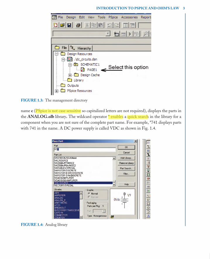
FIGURE 1.3: The management directory
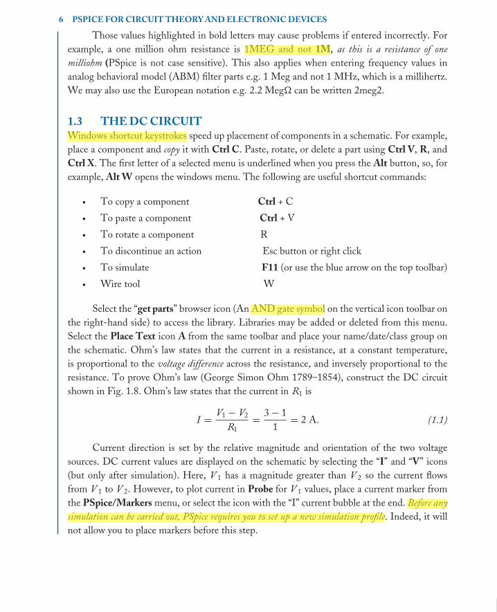
name c (PSpice is not case sensitive so capitalized letters are not required), displays the parts in
the ANALOG.olb library. The wildcard operator * enables a quick search in the library for a
component when you are not sure of the complete part name. For example, *741 displays parts
with 741 in the name. A DC power supply is called VDC as shown in Fig. 1.4.
FIGURE 1.4: Analog library

book Mobk059 March 9, 2007 10:21
4 PSPICE FOR CIRCUIT THEORY AND ELECTRONIC DEVICES
FIGURE 1.5: Select Edit Properties
1.2.1 Moving Components AroundIt is sometimes necessary to manipulate a component in order to place it with a desired
orientation. For example, the uA741 operational amplifier defaults to the noninverting input
topmost when placed. To make the inverting input topmost, select the uA741, right click
the component and select Mirror Vertically. Selecting a component and holding the left
mouse button down enables you to move the component. Use the wire icon (W short-cut)
to connect components. Locate the cursor at one end of the component and press and then
release the left mouse button (Lclick). To draw a wire segment, Lclick the mouse button again
and move the mouse from that component end to another component end. Release the left
mouse button to change direction. Another technique for connecting components is to select a
component, hold the left mouse button and drag to another component, where it should connect.
Select a component (turns green) and Rclick and select the Edit Properties from the list
in Fig. 1.5.
In the spreadsheet section shown in Fig. 1.6, we can add new rows and fill in values in
the A column (more about this later). In this example, select the R2 default value of 1 k� and
replace it by a value e.g. 10k in the Value box.
FIGURE 1.6: Changing the part value

book Mobk059 March 9, 2007 10:21
INTRODUCTION TO PSPICE AND OHM’S LAW 5
FIGURE 1.7: Changing a component value
1.2.2 Display PropertiesSeparate the two connected components to a desired position with the left mouse button held
down. To change a part value from the default value, select the default value and the menu in
Fig. 1.7 will appear.
Replace the 1 k� default value with a 10k � resistor (note there is no space between the 1
and k, and no � symbol. For larger resistance values, you may use the exponent system, so that
10k is entered as 1e4. A 10 nF capacitor is 10n (use letter u for micro –the F is optional), and
ten micro henries is 10u (or 10uH). Be careful about capacitor values: A one farad capacitance is
entered as 1, and not 1F, because this would be interpreted as a very small one Femto capacitor.
Table 1.1 shows the symbol, scale, and name for components.
TABLE 1.1: Cpmponent Units
SYMBOL SCALE NAME
F 1e−15 Femto-
P 1e−12 Pico-
N 1e−9 Nano-
U 1e−6 Micro-
M 1e−3 Milli-
K 1e+3 Kilo-
Meg 1e+6 Mega
G 1e+9 Giga-
T 1e+12 Tera-
book Mobk059 March 9, 2007 10:21
6 PSPICE FOR CIRCUIT THEORY AND ELECTRONIC DEVICES
Those values highlighted in bold letters may cause problems if entered incorrectly. For
example, a one million ohm resistance is 1MEG and not 1M, as this is a resistance of one
milliohm (PSpice is not case sensitive). This also applies when entering frequency values in
analog behavioral model (ABM) filter parts e.g. 1 Meg and not 1 MHz, which is a millihertz.
We may also use the European notation e.g. 2.2 Meg� can be written 2meg2.
1.3 THE DC CIRCUITWindows shortcut keystrokes speed up placement of components in a schematic. For example,
place a component and copy it with Ctrl C. Paste, rotate, or delete a part using Ctrl V, R, and
Ctrl X. The first letter of a selected menu is underlined when you press the Alt button, so, for
example, Alt W opens the windows menu. The following are useful shortcut commands:
r To copy a component Ctrl + C
r To paste a component Ctrl + V
r To rotate a component R
r To discontinue an action Esc button or right click
r To simulate F11 (or use the blue arrow on the top toolbar)
r Wire tool W
Select the “get parts” browser icon (An AND gate symbol on the vertical icon toolbar on
the right-hand side) to access the library. Libraries may be added or deleted from this menu.
Select the Place Text icon A from the same toolbar and place your name/date/class group on
the schematic. Ohm’s law states that the current in a resistance, at a constant temperature,
is proportional to the voltage difference across the resistance, and inversely proportional to the
resistance. To prove Ohm’s law (George Simon Ohm 1789–1854), construct the DC circuit
shown in Fig. 1.8. Ohm’s law states that the current in R1 is
I =V1 − V2
R1=
3 − 1
1= 2 A. (1.1)
Current direction is set by the relative magnitude and orientation of the two voltage
sources. DC current values are displayed on the schematic by selecting the “I” and “V” icons
(but only after simulation). Here, V 1 has a magnitude greater than V 2 so the current flows
from V 1 to V 2. However, to plot current in Probe for V 1 values, place a current marker from
the PSpice/Markers menu, or select the icon with the “I” current bubble at the end. Before any
simulation can be carried out, PSpice requires you to set up a new simulation profile. Indeed, it will
not allow you to place markers before this step.

book Mobk059 March 9, 2007 10:21
INTRODUCTION TO PSPICE AND OHM’S LAW 7
FIGURE 1.8: DC circuit for investigating Ohm’s law
1.3.1 New SimulationIn most electronic simulation software programs, it is necessary to create a simulation profile
before simulating (see Fig. 1.8). Select the New Simulation Profile icon (see the bottom left
icon in Fig. 1.10). When you select this and enter none in the Inherit From box, it will open
up the Simulation Setting menu beside it. We may select in the Inherit From box, an existing
simulation profile with the file extension *.sim. This can be handy if we wish to use previous
profiles and added libraries. The profile specifies what analysis you want and the parameters
necessary for a correct display. This also forces the operator to think about the circuit and
the range of values required for a particular design. The evaluation version of 10.5 contains
more parts than other versions but it does not, however, allow as many parts to be placed and
simulated. Libraries are added when needed and I would suggest that you add the library of
customized parts that are required for certain schematics in this, and my other four books on
PSpice.
All analog schematics must have a ground symbol otherwise a floating error will be displayed .
Ground symbols are placed by selecting, from the icon toolbar on the right, the selection of
ground symbols as shown in Fig. 1.9. Select the one shown that has a little zero beside it, do
not delete or change this in any way. Sometimes this error message is displayed even when
you have a ground part, but this error is fixed by placing a large resistance from the offending
node to ground. You may select and place any ground symbol, select it and change its name to
“zero”.
The most commonly used components are: resistance R, inductance L and capacitance
C in the analog.olb library. Common input signal sources in the source.olb library are: AC
sources, VAC, for frequency response plots and VSIN for transient and frequency response
plots, VDC (DC supply and step signal source), and ground GND (an available icon). Move the
mouse pointer over a library to show its location on the hard disk. To examine the schematic
in greater detail and make it fill the screen, it is necessary to select the third icon from the
book Mobk059 March 9, 2007 10:21
8 PSPICE FOR CIRCUIT THEORY AND ELECTRONIC DEVICES
FIGURE 1.9: The earth or ground symbol
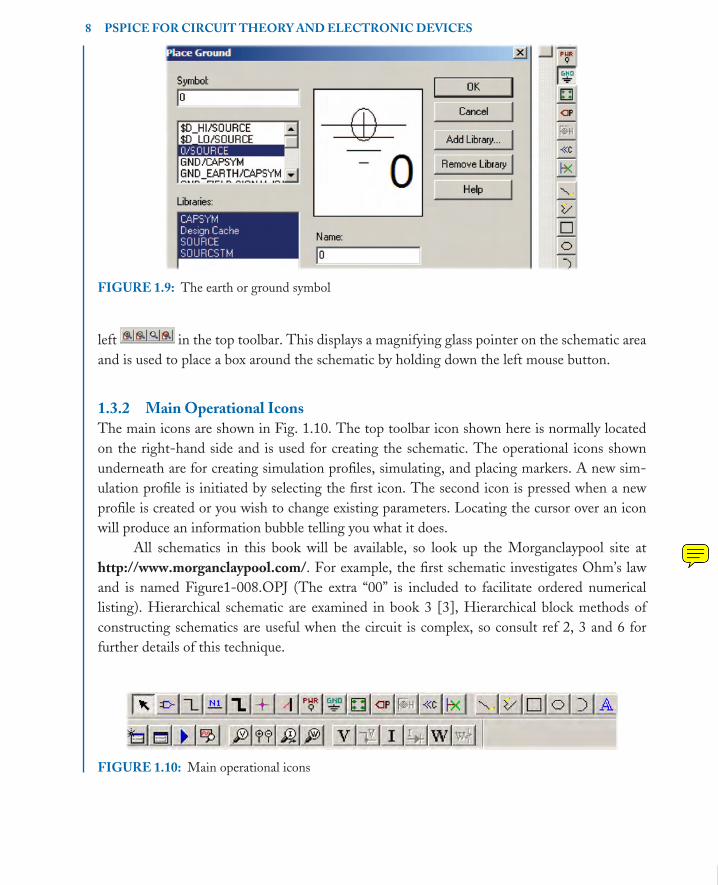
left in the top toolbar. This displays a magnifying glass pointer on the schematic area
and is used to place a box around the schematic by holding down the left mouse button.
1.3.2 Main Operational IconsThe main icons are shown in Fig. 1.10. The top toolbar icon shown here is normally located
on the right-hand side and is used for creating the schematic. The operational icons shown
underneath are for creating simulation profiles, simulating, and placing markers. A new sim-
ulation profile is initiated by selecting the first icon. The second icon is pressed when a new
profile is created or you wish to change existing parameters. Locating the cursor over an icon
will produce an information bubble telling you what it does.
All schematics in this book will be available, so look up the Morganclaypool site at
http://www.morganclaypool.com/. For example, the first schematic investigates Ohm’s law
and is named Figure1-008.OPJ (The extra “00” is included to facilitate ordered numerical
listing). Hierarchical schematic are examined in book 3 [3], Hierarchical block methods of
constructing schematics are useful when the circuit is complex, so consult ref 2, 3 and 6 for
further details of this technique.
FIGURE 1.10: Main operational icons
book Mobk059 March 9, 2007 10:21
INTRODUCTION TO PSPICE AND OHM’S LAW 9
FIGURE 1.11: Sweeping the voltage source V1
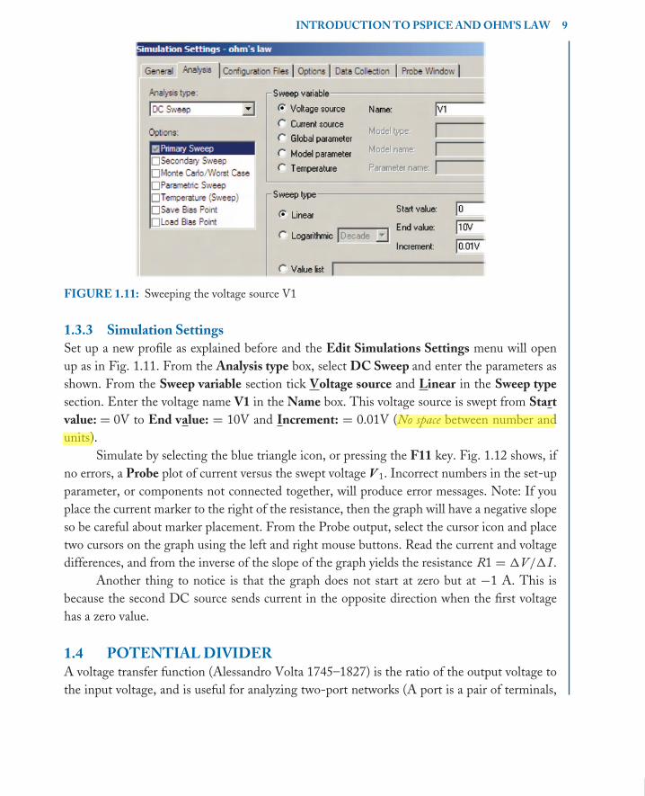
1.3.3 Simulation SettingsSet up a new profile as explained before and the Edit Simulations Settings menu will open
up as in Fig. 1.11. From the Analysis type box, select DC Sweep and enter the parameters as
shown. From the Sweep variable section tick Voltage source and Linear in the Sweep type
section. Enter the voltage name V1 in the Name box. This voltage source is swept from Start
value: = 0V to End value: = 10V and Increment: = 0.01V (No space between number and
units).
Simulate by selecting the blue triangle icon, or pressing the F11 key. Fig. 1.12 shows, if
no errors, a Probe plot of current versus the swept voltage V 1. Incorrect numbers in the set-up
parameter, or components not connected together, will produce error messages. Note: If you
place the current marker to the right of the resistance, then the graph will have a negative slope
so be careful about marker placement. From the Probe output, select the cursor icon and place
two cursors on the graph using the left and right mouse buttons. Read the current and voltage
differences, and from the inverse of the slope of the graph yields the resistance R1 = 1V/1I .
Another thing to notice is that the graph does not start at zero but at −1 A. This is
because the second DC source sends current in the opposite direction when the first voltage
has a zero value.
1.4 POTENTIAL DIVIDERA voltage transfer function (Alessandro Volta 1745–1827) is the ratio of the output voltage to
the input voltage, and is useful for analyzing two-port networks (A port is a pair of terminals,
book Mobk059 March 9, 2007 10:21
10 PSPICE FOR CIRCUIT THEORY AND ELECTRONIC DEVICES
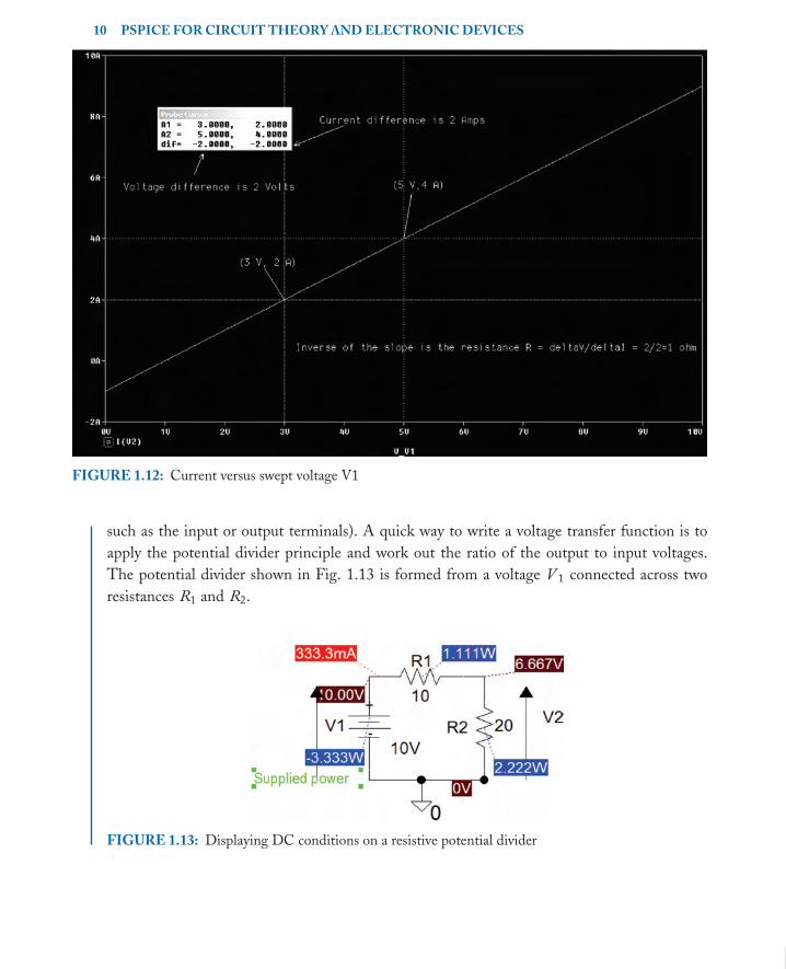
FIGURE 1.12: Current versus swept voltage V1
such as the input or output terminals). A quick way to write a voltage transfer function is to
apply the potential divider principle and work out the ratio of the output to input voltages.
The potential divider shown in Fig. 1.13 is formed from a voltage V 1 connected across two
resistances R1 and R2.
FIGURE 1.13: Displaying DC conditions on a resistive potential divider

book Mobk059 March 9, 2007 10:21
INTRODUCTION TO PSPICE AND OHM’S LAW 11
FIGURE 1.14: Current divider network
The transfer function is obtained by substituting the total current I = V1/(R1 + R2) into
the output voltage V2 = I R2.
V2 =
(
V1
R1 + R2
)
R2 ⇒V2
V1=
R2
R1 + R2. (1.2)
Select the V I icons for displaying DC conditions. The new W icon shows the power
supplied to the circuit and the power dissipated in each resistor after simulation.
1.4.1 Current DividerThe current-divider circuit in Fig. 1.14 shows a current DC source called IDC placed in parallel
with R1 and R2. The current transfer function is a ratio of output and input currents Iout/Iin.
The voltage across the two resistors is
V = I1 R1 = I2 R2 = IDC RT. (1.3)
I 1 and I 2 are the currents in R1 and R2, and RT is the total resistance. The input current is IDC
and the output current is I2 (Andre Ampere 1775–1836). Substituting the total resistanceRT =
R1 R2/(R1 + R2) into (1.3) gives the current in the second resistor I2 = IDC RT/R2, hence the
current transfer function is
I2 R2 = IDC RT ⇒I2
IDC=
RT
R2=
R1 R2
(R1 + R2)R2=
R1
R1 + R2. (1.4)
Select the DC current icon and press the F11 key to simulate. The current in each
resistance is
I2 =R1 IDC
R1 + R2=
1k.1
1k + 2kA = 0.333A (1.5)
I1 =R2 IDC
R1 + R2=
2k.1
1k + 2kA = 0.666A. (1.6)

book Mobk059 March 9, 2007 10:21
12 PSPICE FOR CIRCUIT THEORY AND ELECTRONIC DEVICES
Compare displayed current values to those calculated in each resistor using equations
(1.5) and (1.6). We can also use the Watt marker icon for displaying power on the schematic.
The source power is displayed as 677 W = 677 V × 1A. Note: all PSpice current and voltage
sources (AC and DC) are ideal and it is always a good idea to include some resistances to
represent the nonideal source situation. A current source has a large value resistance placed in
parallel with it. For a voltage source the source resistance is small and should be placed in series
with the voltage.
1.5 EXERCISES(1) Investigate resistive loading on voltage and current dividers by placing a resistance
in parallel with the output resistance, R2. How does loading change the output volt-
age/current?
(2) Repeat exercise (1) but investigate loading on the current divider.

book Mobk059 March 9, 2007 10:21
13
C H A P T E R 2
The DC Circuit and Kirchhoff’s Laws
2.1 MAXIMUM POWER TRANSFERMaximum power is transferred from a source to an equal-value load and is proved by differen-
tiating the output power with respect to the load resistance and equating to zero. The potential
divider in Fig. 2.1 demonstrates maximum power transfer from the source, V source, and source
resistance, R source, to a varying load RL.
2.1.1 Param PartIn this example, select the RL default value of 1 k� and replace it by a name of your choice
e.g. {Rvar} in the Name box of the Display Parameter menu. The variable resistance name
must be enclosed in curly brackets{}. However, the Rvar name has no significance and can be
any name you choose. The PARAM part, from the SPECIAL.OLB library, is very useful for
investigating circuit behavior for a range of part values. This part, however, is used and accessed
in a different manner to that in previous versions of PSpice. What is required is to place the
part using the little AND gate symbol, and when selected it turns green. Rclick and select Edit
Properties to display the spreadsheet shown in Fig. 2.2. In this spreadsheet, we may add new
rows and assign values in the A column. There is now no limit to the number of parameters
you may add in version 10.5, unlike the PARAM part in version 8, which was limited to three
parameters.
Select New Row and enter Rvar in the Name: box but NO curly brackets, and the
nominal value of 300 � in the Value box as shown in Fig. 2.3.
2.1.2 Simulation SettingsPress Edit Simulation Settings icon or select the PSpice/New Simulation Profile menu.
Select DC Sweep and enter the parameters shown in Fig. 2.4. Rvar is varied Linearly from 1
to 300 � in Increments of 1 �.
An alternative to the above procedure is to specify a list of values separated by spaces in
the Value list box.

book Mobk059 March 9, 2007 10:21
14 PSPICE FOR CIRCUIT THEORY AND ELECTRONIC DEVICES
FIGURE 2.1: Potential divider with variable load
FIGURE 2.2: Edit Properties Param parameters
FIGURE 2.3: The Param part parameters

book Mobk059 March 9, 2007 10:21
THE DC CIRCUIT AND KIRCHHOFF’S LAWS 15
FIGURE 2.4: Analysis and DC sweep
2.1.3 Trace Expression BoxPress F11 and a blank Probe screen appears since no markers were placed on the schematic. To
display power dissipated in a device, we may use one of the two techniques. The first technique
uses the power marker (W icon) that is located in the middle of the device as shown. The second
technique is the manual method accessed from the Probe screen after simulation when you
select the Trace add icon (Or press the Insert button on the keyboard). Enter the expression
for the load power as I(R2)*V1(R2) in the Trace Expression box shown in Fig. 2.5.
Note: The resistance orientation has an effect on the final Probe display. If the display
comes out upside down, then the resistor is the wrong way around and should be rotated around
180◦ (the R key), or place a minus sign in front of the current–voltage product. Component
orientation is how PSpice handles conventional current direction flow in R, L, and C , so be
careful about the way you place them and marker placement. Fig. 2.6 shows the Probe plot
when cursors are placed using the left and right mouse buttons. Maximum power is measured
FIGURE 2.5: Adding variables

book Mobk059 March 9, 2007 10:21
16 PSPICE FOR CIRCUIT THEORY AND ELECTRONIC DEVICES
FIGURE 2.6: Power versus Rvar (Linear x-axis variable)
by selecting the maximum Cursor Peak icons to locate the cursor at the maximum power
value. Compare the measured maximum power to the value in (2.1).
Pmax = I 2 RL =
[
V source
Rsource + RL
]2
RL =
[
V source
RL + RL
]2
RL =V source2
4RL=
100
4 × 10= 2.5 W
(2.1)
From Probe, select Plot /Label to access a menu bar containing many useful display
graphic tools such as Text, line, Arrows, Box. The plot is copied to clipboard from the
Probe/Windows where you have the option of copying with a white or black background.
2.2 CHANGING THE X -AXIS VARIABLEThere are times when you need to change the axis properties such as to change the scale, linear
to log, or to change the swept variable. The sub-menu in Fig. 2.7 is accessed by selecting the
space beside any x-axis number in Probe, or by selecting the Trace menu. Tick Log to change
the x-axis to logarithmic (or select the log icon ). A new feature is that we may now place an
x-axis name by selecting Axis Title. We may change the x- and y-axis range in the Data Range
box. The x and y grid display can also be changed to the simple display shown in Fig. 2.6. Add

book Mobk059 March 9, 2007 10:21
THE DC CIRCUIT AND KIRCHHOFF’S LAWS 17
FIGURE 2.7: Changing the x-axis variable
a y-axis title by selecting the y-axis space and entering “Maximum Power Transfer” in the Axis
Title (a title may be added to the x-axis as well). The Probe plot may be copied to clipboard
from the Windows/Copy to Clipboard menu where options are offered such as making the
background transparent.
2.2.1 The Log CommandAll key strokes pressed whilst in the Probe environment can be recorded and a file created that
can be accessed later from Probe after simulation. This file when run automatically reruns the
key pressed sequence to produce the desired Probe screen. This log command file is created by
ticking Log Commands from the Probe/File/ menu where you enter a name such as Figure2-
008.cmd and save. You must un-tick Log Commands when you are finished recording all key
presses. If you need to re-simulate with different parameters/designs for example, then select
Probe/File/Run Commands and open Figure2-008.cmd. This can be accessed at any time
from the probe menu. Fig. 2.8 is not very complicated and hence it is not really necessary here
but is very useful when you need to display several plots on different levels. The FFT icon can
also be included in this file.
2.3 MESH ANALYSISKirchhoff’s voltage law (Gustav Kirchhoff 1824–1887) states that the sum of the potential drops
and voltage sources around a closed loop is zero. We may write the mesh voltages’ equations

book Mobk059 March 9, 2007 10:21
18 PSPICE FOR CIRCUIT THEORY AND ELECTRONIC DEVICES
FIGURE 2.8: Power versus Rvar (log x-axis variable)
in a simple and safe manner by assigning all mesh currents in the same clockwise direction. For
example, the Tee network (a popular resistive attenuator) in Fig. 2.9 has two sources E1 and E2
(VDC parts) and a self-impedances in loop one R1 + R3 and R2 + R3 in loop 2. Both impedances
are made positive and the mutual impedance between the loops is −R3.
The sum of the impedances in a loop is called the self-impedance and is assigned a positive
sign, whereas the impedance common to two loops is called the mutual impedance and is always
FIGURE 2.9: A Tee network

book Mobk059 March 9, 2007 10:21
THE DC CIRCUIT AND KIRCHHOFF’S LAWS 19
negative. A negative sign is assigned to each voltage source when the assigned current direction
is in the opposite direction to the rise in a voltage source. Assign all mesh currents in the same
direction and applying Kirchhoff’s voltage law to yield
Loop 1 E1 = I1 R1 + I1 R3 − I2 R3 (2.2)
Loop 2 − E2 = −I1 R3 + I2 R2 + I2 R3. (2.3)
Loop 2 shows a negative sign in front of E2 because the current direction is in the opposite
direction to the rise in the potential of E2. Applying these simple rules means we may write
the equations in a quick and easy manner, and with less chance of making mistakes. However,
(2.2) and (2.3) may be written directly as
E1 = I1(R1 + R3) − I2 R3 (2.4)
−E2 = −I1 R3 + I2(R2 + R3). (2.5)
The sum of the self-impedances in a loop is positive and equal to R1 + R3 in loop 1 and
R2 + R3 in loop 2. The mutual impedance is negative and equal to −R3 in both equations. The
loop equations in matrix form are
[
E1
−E2
]
=
[
I1
I2
] [
(R1 + R3) (−R3)
(−R3) (R2 + R3)
]
. (2.6)
The loop currents are calculated by applying Cramer’s rule to (2.6) as
I1 =
[
E1
−E2
(−R3)
(R2 + R3)
]
[
(R1 + R3) (−R3)
(−R3) (R2 + R3)
]
=E1((R2 + R3) − (−E2)((−R3)
(R1 + R3)(R2 + R3) − (−R3)(−R3)=
1 × 70 − 1 × 50
60 × 70 − 2500= 11.8 mA (2.7)
I2 =
[
(R1 + R3)
(−R3)
E1
−E2
]
[
(R1 + R3) (−R3)
(−R3) (R2 + R3)
]
=−E2((R2 + R3) − (E1)((−R3)
1700=
−1.60 + 1.50
1700=
−10
1700= 5.9 mA. (2.8)

book Mobk059 March 9, 2007 10:21
20 PSPICE FOR CIRCUIT THEORY AND ELECTRONIC DEVICES
A negative value for the loop current tells you that the current direction is opposite to
your assigned direction.
2.4 NODAL ANALYSISNodal analysis is used to solve for the voltage vx at the junction (node) of R1, R2, and R3 in
Fig 2.9. Applying Kirchhoff’s current law at the node which states that the sum of the currents
at a node is zero:
I1 + I2 + I3 = 0. (2.9)
We may express each current in terms of the voltages and resistances:
(vx − V1)
R1+
(vx − V2)
R2+
(vx − 0)
R3= 0. (2.10)
This technique may generate errors in your analysis because of confusion over current
and voltage directions. A better technique is to write the node voltage equation using a similar
method to that used in mesh analysis. The method is as follows: Show all current directions in
the same direction coming out of a node. This contradicts the normal laws of energy conservation
but is done for the reasons discussed in mesh analysis. Name the node under investigation vx,
a voltage with respect to the ground (the reference node). An admittance connected to this
node is called a self-admittance and is made positive, whereas admittances connected between vx
and any adjacent nodes are called mutual-admittances and are made negative. A voltage source
attached via admittance to the vx node is made negative. Thus, we write the nodal equation at
the junction of R1, R2, and R3 using this method as
vx
(
1
R1+
1
R2+
1
R3
)
−V1
R1−
V2
R3= 0. (2.11)
Substitute component values and solve for the node voltage vx as
vx
(
1
10+
1
20+
1
50
)
−1
10−
1
20= 0 ⇒ vx (0.17) = 0.15 ⇒ vx = 0.882 V. (2.12)
Press F11 and select the V and I icons to display current and voltage values on the
schematic. The displayed values might be slightly different from the calculated ones because of
the number of places of decimals or Significant Digits. However, you may change the number
of displayed digits by selecting the menu sequence in Fig. 2.10.

book Mobk059 March 9, 2007 10:21
THE DC CIRCUIT AND KIRCHHOFF’S LAWS 21
FIGURE 2.10: Changing the digits
Select the PSpice/Bias Points/Preferences menu. Enter 4 in the Displayed Precision
as shown in Fig. 2.11 and it will display the number to four decimal points.
After simulation, select the V/I icons to display DC current and voltages shown in
Fig. 2.12.
To remove redundant voltage or current displays, press the icon to the right of the voltage
or current icons. To add extra voltage displays on a wire, select the wire and press the little node
junction icon beside the main V icon. Make sure Bias Point is ticked in the Analysis Setup
menu.
FIGURE 2.11: Setting the digits
book Mobk059 March 9, 2007 10:21
22 PSPICE FOR CIRCUIT THEORY AND ELECTRONIC DEVICES
FIGURE 2.12: Displaying DC conditions
R1
10k
R2
10k
C11u
C2
1u
0
V2
FREQ = 1k
VAMPL = 1
VOFF = 0
V1
FREQ = 1kVAMPL = 1VOFF = 0
VV
FIGURE 2.13: Part of a Sallen and Key active filter
2.5 EXERCISES(1) In Fig. 2.1, vary the source resistance and investigate maximum power transfer. (Hint:
An ideal voltage has a zero resistance source hence all power is absorbed by the
load.)
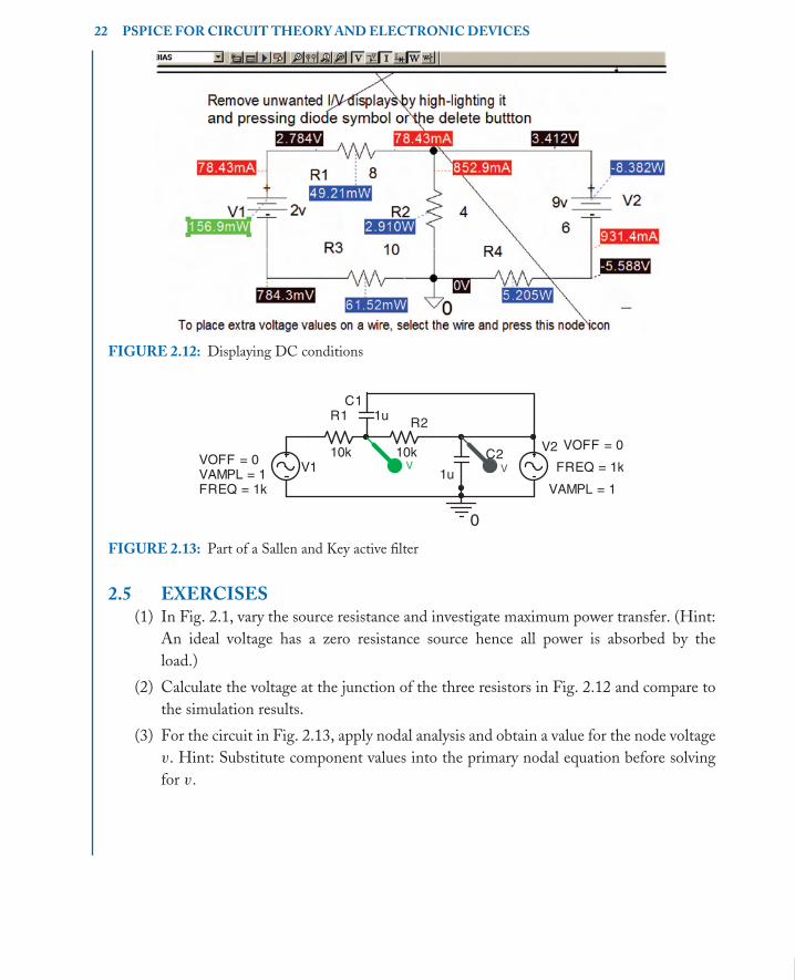
(2) Calculate the voltage at the junction of the three resistors in Fig. 2.12 and compare to
the simulation results.
(3) For the circuit in Fig. 2.13, apply nodal analysis and obtain a value for the node voltage
v. Hint: Substitute component values into the primary nodal equation before solving
for v.

book Mobk059 March 9, 2007 10:21
23
C H A P T E R 3
Transient Circuits and LaplaceTransforms
3.1 TRANSIENT ANALYSISComplex signals, such as step or pulse-type signals applied to CR, LR circuits, and LCR
circuits, are analyzed in a much simpler fashion using the Laplace transform (Pierre Laplace
1749–1825). Laplace tables and partial fraction expansion methods are used when transforming
from the s-domain back to the time domain.
3.2 LAPLACE TRANSFORM AND CAPACITANCEThe Laplace Transform of a function f (t) is
LT{ f (t)} = F(s ) =
∫
∞
0
f (t)e−s tdt (3.1)
The current–voltage relationship for a capacitor in the time domain, with an initial voltage
across the capacitor plates V0 (consider this as a step voltage), is
vC (t) =1
C
∫ t
0
i(t)dt + V0 (3.2)
Laplace transforming equation (3.2):
LT{vC (t)} = LT
{
1
C
∫ t
0
i(t)dt + V0
}
(3.3)
The Laplace transform for integration and step functions, is 1/s, hence (3.3) becomes
Vc (s ) =1
s CIc (s ) +
V0
s(3.4)
All transformed circuit variables are shown capitalized in the Laplace equivalent circuit.
Figs. 3.1(a) and 3.1(b) show a capacitor representation in the time and s domains where
the reactance 1/sC I is in series with the initial condition voltage, V0/s, but acting in the sense
shown in Fig. 3.1(b).

book Mobk059 March 9, 2007 10:21
24 PSPICE FOR CIRCUIT THEORY AND ELECTRONIC DEVICES
FIGURE 3.1: Transformed capacitance
3.3 INDUCTANCEThe current–voltage–time relationship for an inductor, with an initial current, I0, is
vL(t) = Ldi
dt+ I0 (3.5)
The Laplace transform of (3.5) is
LT{vL(t)} = VL(s ) = LT
(
Ldi
dt+ I0
)
= s LI (s ) − LI0 (3.6)
An inductor representation in the time domain is shown in Fig. 3.2(a) and the Laplace transform
of an inductor is shown in Fig. 3.2(b) as a reactance sL ohms in series with the initial condition
voltage, LI Volts but in the same direction as the input voltage.
The transformed circuit may also be expressed as a Norton equivalent circuit with the
Norton admittance in parallel with a current source.
3.4 FIRST-ORDER CR AND LR CIRCUITSFigure 3.3 shows a high-pass filter that is used to couple amplifier stages together for the
purposes of DC isolating each stage. A pair of differential markers measures the voltage across
FIGURE 3.2: Transformed inductance

book Mobk059 March 9, 2007 10:21
TRANSIENT CIRCUITS AND LAPLACE TRANSFORMS 25
FIGURE 3.3: High-pass CR circuit
a component that is not connected to the ground reference point, such as the voltage across the
capacitor. Select the PSpice/Markers/ Voltage Differential to place two consecutive markers,
where one marker has a plus symbol and the other has a negative symbol (or use the icons from
the top marker icon toolbar).
Apply the Laplace transform and obtain expressions for the capacitor and resistor voltages.
We may obtain current or voltage expressions in time using the inverse Laplace transform table
given in the appendix. After simulation, compare your calculations to the simulation results for
currents and voltages evaluated at certain times. The Sw tClose switch part from the eval.olb
library is closed at time t = 0 s (Assume the capacitor is initially uncharged). Evaluate the
capacitor voltage at t = 5 s, where V 1 = 10 V, R1 = 2 �, C = 1 F. Capacitance entered in
PSpice as 1 F (no space between the number and the unit) is interpreted as 1 Femto farads—a
much smaller capacitor, so leave out the F symbol.
3.4.1 SolutionThe first switch, sw tClose, closes at a certain time (Note: the sw tOpen switch opens at a
specified time). DLclick the sw tClose part to set the following parameters:
Time to close = TCLOSE = 0 s,
Transient time = TTRAN = 1 us,
Switch resistance when closed = RCLOSED = 0.01 �, and
Switch resistance when opened = ROPEN = 1 Meg
Other mechanical switches are available in the discrete.olb library. The voltage across the
capacitor increases exponentially because the current into the capacitor accumulates charge on
the capacitor plates. The capacitor current, however, decreases exponentially with time because
the capacitor voltage that is building up with time opposes the source voltage. The circuit time
constant, τ = CR, is the time it takes for the capacitor voltage to charge up to 63 % of the applied
step voltage. The time constant is also found by extrapolating the initial slope of the capacitor
voltage with a straight line until it intersects a line drawn across from the final capacitor voltage
to the y-axis. The time constant τ is then measured by dropping a perpendicular line from

book Mobk059 March 9, 2007 10:21
26 PSPICE FOR CIRCUIT THEORY AND ELECTRONIC DEVICES
the intercept to the time axis. The Laplace transform for a step voltage V1 is V1/s , hence the
current is the step voltage divided by the total circuit impedance R+ 1/sC as
IR(s ) =Voltage
Impedance=
10/s
2 + 1/s=
10
2s + 1=
5
s + 1/2=
5
s + 0.5(3.7)
From the Laplace tables, we see that the inverse Laplace transform of 1/(s + a) is e−at , where
a = 0.5 so that Eq. (3.7) when converted to the time domain is 5e−0.5t. The current at t = 5 s
is
iR(t) = 5e−0.5t∣
∣
∣
t=5⇒ iR(5) = 5e−0.5×5
= 5e−2.5= 0.414 A (3.8)
3.4.2 Partial Fraction ExpansionPartial fraction expansion (PFE) is necessary to transform an equation in s , back to an equation
in time, where the equation in s has no direct equivalent in the Laplace tables. For example,
the capacitor voltage in the previous example is obtained by multiplying the current in (3.8) by
the capacitor reactance to yield
Vc (s ) = I (s )
(
1
s C
)
=
(
5
s + 0.5
) (
1
s
)
= 51
(s + 0.5)(s )(3.9)
The two functions 1/(s + 0.5) and 1/s are in the Laplace tables, but the product of the two is
not, so we need to separate the parts using the partial fraction expansion method. The constant
5 is temporarily ignored, so separate the two parts in (3.9) by introducing two new constants A
and B as
1
(s + 0.5)(s )=
A
(s + 0.5)+
B
(s )=
A(s ) + B(s + 0.5)
(s + 0.5)(s )=
(A + B)s + B0.5)
(s + 0.5)(s )(3.10)
Combine all s terms and equate the right and left terms of the top part of (3.10) i.e.
1 = (A + B)(s ) + B0.5 ⇒ (A + B)(s ) = 0 and 0.5B = 1 ⇒ B = 2 (3.11)
Now A + B = 0 since s is not zero and there are no s terms on the LHS of (3.11). This implies
that A = −B = −2. Substitute these values back into (3.10):
Vc (s ) =
(
5
s + 0.5
)(
1
s
)
= 51
(s + 0.5)(s )= 5
[
2
s−
2
s + 0.5
]
= 10
[
1
s−
1
s + 0.5
]
(3.12)
The inverse Laplace equivalent for the two parts of (3.12) yields the capacitor voltage in the
time domain as
vc (t) = 10(1 − e−0.5t) V (3.13)
book Mobk059 March 9, 2007 10:21
TRANSIENT CIRCUITS AND LAPLACE TRANSFORMS 27
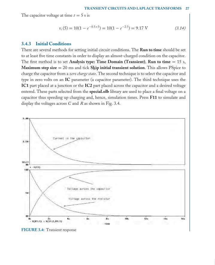
The capacitor voltage at time t = 5 s is
vc (5) = 10(1 − e−0.5×5) = 10(1 − e−2.5) = 9.17 V (3.14)
3.4.3 Initial ConditionsThere are several methods for setting initial circuit conditions. The Run to time should be set
to at least five time constants in order to display an almost-charged condition on the capacitor.
The first method is to set Analysis type: Time Domain (Transient), Run to time = 15 s,
Maximum step size = 20 ms and tick Skip initial transient solution. This allows PSpice to
charge the capacitor from a zero charge state. The second technique is to select the capacitor and
type in zero volts on an IC parameter (a capacitor parameter). The third technique uses the
IC1 part placed at a junction or the IC2 part placed across the capacitor and a desired voltage
entered. These parts selected from the special.olb library are used to place a final voltage on a
capacitor thus speeding up charging and, hence, simulation times. Press F11 to simulate and
display the voltages across C and R as shown in Fig. 3.4.
FIGURE 3.4: Transient response

book Mobk059 March 9, 2007 10:21
28 PSPICE FOR CIRCUIT THEORY AND ELECTRONIC DEVICES
FIGURE 3.5: The original and Thevenin equivalent circuits
3.5 EXAMPLE 2Fig. 3.5 shows an electrical circuit and the Thevenin equivalent circuit. With C initially
uncharged at time t = 0 s, and switch S1 (Sw tOpen part) closed, the capacitor starts to
charge. Switch S2 (Sw tClose part) is then closed, and S1 opened simultaneously after 3 s.
Obtain an expression, using the Laplace Transform, for the current in C as a function of s
(Hint: Apply Thevenin’s theorem to the left of C , treating C as the load). Obtain an expression
in time for the capacitor voltage and evaluate it at t = 3 s. V 1 = 20 V, R1 = R2 = 4 �,
C = 1 F.
3.5.1 SolutionThe original circuit is simplified by applying Thevenin’s theorem to yield an equivalent resistance
of 2 � because the resistors are now in parallel when you replace the voltage source by a short-
circuit link. In this example, the source is considered an ideal voltage source, and hence has a
zero source resistance. The voltage at the junction of the two resistors to the left of the capacitor
is determined by applying the potential divider principle. Remove the load C . The Thevenin
equivalent voltage is (10/s ) V, i.e. half the input voltage (look up potential divider in the index).
The complete equivalent circuit is shown at the right in Fig. 3.5. The current is calculated by
dividing the Thevenin step voltage by the circuit impedance as
IR(s ) =10/s
2 + 1/s
( s
s
)
=10
2s + 1÷
2
2=
5
s + 1/2=
5
s + 0.5
From the Laplace tables in Appendix A, we convert IR(s ) to current as a function of time
IR(t) = 5e−0.5t

book Mobk059 March 9, 2007 10:21
TRANSIENT CIRCUITS AND LAPLACE TRANSFORMS 29
The current at 3 s is IR(3) = 5e−0.5×3= 5e−1.5
= 1.11 A. An expression for the capacitor
voltage is obtained by multiplying the current by the capacitor reactance as
Vc (s ) = IR(s )
(
1
s C
)
=
(
5
s + 0.5
) (
1
s
)
There are no entries in the Laplace tables for this product, so we need to apply PFE in order
to separate the voltage expression into two functions that are in the tables. For example:
51
(s + 0.5)(s )= 5
(
A
s + 0.5+
B
s
)
= 5
(
A(s ) + B(s + 0.5)
(s + 0.5)(s )
)
= 5
(
(A + B)s + B0.5)
(s + 0.5)(s )
)
To determine A and B, equate the top part of the left-hand side of this equation to the RHS:
1 = (A + B)(s ) + B0.5 ⇒ (A + B)(s ) = 0 ⇒ (A + B) = 0 ⇒ A = −B
This means that 1 = 0.5B ⇒ B = 2
V c (s ) = I (s )
(
1
s C
)
=
(
5
s + 0.5
)(
1
s
)
= 5
[
2
s−
2
s + 0.5
]
= 10
[
1
s−
1
s + 0.5
]
From the Laplace tables, we see that 1/s is equivalent to 1 in the time domain and 1/(s + 0.5)
is equivalent to e−0.5t . The capacitor voltage in the time domain is
vc (t) = 10(1 − e−0.5t) V
At t = 3 s, the 20 V supply is disconnected by opening S1 and closing S2, thus allowing the
capacitor to charge to vc (3) = 10(1 − e−0.5×3) = 7.76 V. The circuit now comprises a voltage
source 7.76/s V in series with a 2 � resistance and a 1 F capacitor. However, this voltage source is
not a constant voltage supply and so decays exponentially vc (t) = 10e−0.5t . The current changes
direction instantaneously because the capacitor cannot charge instantaneously but decays in an
exponential manner. Select the Analysis/Transient menu and set Run to time to 15 s and
Maximum step size (default value). Press F11 to simulate and produce the current and voltage
waveforms shown in Fig. 3.6.
3.6 EXAMPLE 3Fig. 3.7 shows a switch open for a long time which is then closed at t = 0.2 s. Obtain
an expression for the inductor current as a function of s . Using the Laplace tables, get an
expression for the inductor current in time and evaluate at t = 0, 0.2 and 0.3 s. Assume zero
initial conditions and R1 = R2 = 5 �, L = 2 H, V1 = 1 V.

book Mobk059 March 9, 2007 10:21
30 PSPICE FOR CIRCUIT THEORY AND ELECTRONIC DEVICES
FIGURE 3.6: Current and voltage waveforms
3.6.1 SolutionLaplace transforming the circuit yields the current as
IL(s ) =1/s
2s + 10=
1
s
1
2s + 10=
1
(s )
1/2
(s + 5)= 0.5
[
1
(s )(s + 5)
]
=A
s+
B
s + 5
V1 1
+
-
U1 TCLOSE = 0.2s1 2
R1 5 R2 5
L1 2
0
I
V
FIGURE 3.7: Switch closed at 0.2 s

book Mobk059 March 9, 2007 10:21
TRANSIENT CIRCUITS AND LAPLACE TRANSFORMS 31
FIGURE 3.8: Inductor current
Ignore the 0.5 factor and equate the top left-hand side of the equation to the right-hand side as
1 = (A + B)(s ) + A5 ⇒ A = 1/5 and (A + B)(s ) = 0 ⇒ (A + B) = 0, or, B = −A = −1/5
Another method of solving PFE coefficients is [ 1s +5 ]S=0 ⇒ A =
15 and [ 1
s ]S=−5 ⇒ B = −15
IL(s ) = 0.5
[
1/5
s−
1/5
s + 5
]
=0.5
5
[
1
s−
1
s + 5
]
= 0.1(1 − e−5t)
The current at t = 0.2 s is i = 63 mA (see Fig. 3.8). Closing the switch at t = 0.2 s reduces
the circuit resistance to 5 �, However, the inductor initial voltage is now equal to the current at
0.2 s multiplied by the inductance, i.e. VL = I (0.2)L = (63 mA)(2 Henries) = 0.106 V. The
initial voltage direction is in the opposite direction to the voltage drop across the inductance.
The current is the voltage (1/s + 0.106)/impedance i.e.
IL(s ) =1/s + 0.126
2s + 5=
1/2s
s + 2.5+
0.063
s + 2.5=
0.5
(s )(s + 2.5)+
0.063
s + 2.5

book Mobk059 March 9, 2007 10:21
32 PSPICE FOR CIRCUIT THEORY AND ELECTRONIC DEVICES
Apply partial fraction expansion to the first part 1(s )(s +2.5) = [ A
s +B
s +2.5 ] and solve
[
1
s + 2.5
]
S=0
⇒ A =1
2.5and
[
1
s
]
S=−2.5
⇒ B = −1
2.5
IL(s ) = 0.5
[
1/2.5
s−
1/2.5
s + 2.5
]
+0.063
s + 2.5=
.5
2.5
[
1
s−
1
s + 2.5
]
+0.063
s + 2.5
This current as a function of time is written from the Laplace tables as
IL(t) = 0.2(1 − e−2.5t) + 0.063e−2.5t mA
Note: We evaluate this last expression at t = 0.3 s by substituting the elapsed time of 0.1 s =
(0.3 s–0.2 s), and not 0.3 s, which is the total time.
IL(0.1) = 0.2(1 − e−2.5×0.1) + 0.063e−2.5×0.1= 92 mA
Set Run to time = 3 s, Maximum step size = 500 u. Press F11 to simulate to display the
inductor current in Fig. 3.8.
Note the inductor voltage has a distinct discontinuity at the time of switching.
3.7 EXAMPLE 4The switch in Fig. 3.9 is initially opened and then closed at t = 80 ms. Using the Laplace
transform, obtain an expression in s for the inductor current. Hence, calculate a value for
the inductor current at t = 80 ms. Assume the inductor is initially uncharged. R1 = 5 �,
R2 = 20 �, L = 0.1 H, I1 = 2 A, I2 = 3 A.
FIGURE 3.9: Problem 4 using parallel current sources

book Mobk059 March 9, 2007 10:21
TRANSIENT CIRCUITS AND LAPLACE TRANSFORMS 33
3.7.1 SolutionBefore the switch is closed, calculate the inductor current by applying the current divider
principle to I1, R2, and L1:
IL(s ) =2
s
20
20 + s 0.1=
(
2
s
) (
200
200 + s
)
=400
s
1
(200 + s )= 400
[
A
s+
B
s + 200
]
Solve for A and B using partial fraction expansion [ 1s +200 ]s =0 ⇒ A =
1200 and [ 1
s ]s =−200 ⇒
B = −1
200 .
IL(s ) =400
200
[
1 −1
s + 200
]
⇒ IL(t) = 2[
1 − e−200t]
A
When the switch is closed at t = 80 ms, the inductor current is IL(80 ms) = 2(1 −
e−200×80ms) = 2 A. The initial inductor current I0 produces a back EMF I0 = 80 mV. The
equivalent circuit is a generator in series with the inductor reactance. Complete the solution
by combining the two current sources into one source and the two resistances into one resis-
tance. Set Analysis to Analysis type: Time Domain (Transient), Run to time = 500 ms, and
Maximum step size = 10 us. Press F11 to plot the inductor current shown in Fig. 3.10.
FIGURE 3.10: Inductor current
book Mobk059 March 9, 2007 10:21
34 PSPICE FOR CIRCUIT THEORY AND ELECTRONIC DEVICES
C110u
R1
1k
V3 1V
+
-
V115
+
-
L1
1
R5
5
V4 1
+
-
L2
2
U1
TOPEN = 0.02
1 2
V5
2v
+
-
V7
.67
+
-
V6
.67
+
-
U3
TCLOSE = 0.2
1 2
U7
TOPEN = 0.75ms
1 2
U6
TCLOSE = 0.75ms
1
2 R9
2.5
V81
+
-
C2 1
R65
R2 5k
U2TCLOSE = 0.02
1
2
U5
TCLOSE = 0
1 2
V2 1V
+
-
U8
TCLOSE = 2 1 2
C3
1
R8
2.5
R31 R41
U4
TCLOSE = 0.1
1 2
R7
0.133m
0
0 00
0
I
I
I
V
I V
FIGURE 3.11: Switching circuits
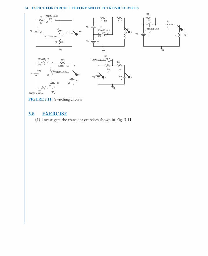
3.8 EXERCISE(1) Investigate the transient exercises shown in Fig. 3.11.

book Mobk059 March 9, 2007 10:21
35
C H A P T E R 4
Transfer Functions and SystemParameters
4.1 TRANSFER FUNCTIONSA transfer function comprises numerator and denominator parts with each part containing one
or more factors. We may use a LAPLACE part to plot the transfer function frequency response
or the impulse response. The default Laplace part has a unity numerator and denominator is
1 + s, which is a low-pass filter with a 1 rs−1 cut-off frequency. Each transfer function factor
entered is separated by a multiplier operator “*”. For example, if the numerator is 5 s, then enter
it as 5*s. A fourth-order polynomial, factored into two second-order polynomials, has each
polynomial enclosed by brackets () but separated by a “*” symbol between each pair of brackets.
4.2 BUTTERWORTH TRANSFER FUNCTIONS AND THELAPLACE PART
A second-order transfer function is formed from an inverted second-order Butterworth
loss function with a cut-off frequency ω20 = 100 ⇒ ω0 = 10 rs−1
⇒ f0 = 10 rs−1/(2π ) =
1.59 Hz. The Butterworth loss function is de-normalized by replacing the normalized complex
frequency variable $ with the complex frequency variable, s , divided by the cut-off frequency
[ref: 1]. The transfer function is therefore
H(s ) =Vout
Vin=
1
$2 + 1.414$ + 1
∣
∣
∣
∣
$=s /10
=1
( s10 )2 + 1.414 s
10 + 1=
100
s 2 + 14.14s + 100(4.1)
Draw the schematic in Fig. 4.1 and use the Net Alias icon to place a name on the output wire.
Select the Laplace part, Rclick and select Edit Properties. In the DENOMinator box,
enter the transfer function denominator (s ∗s + 14.14∗s + 100), and 100 in the NUMerator
box. In the top right-hand corner press the small x to exit the properties. To plot the frequency
response, place a dB marker (From the PSpice/Markers/Advanced menu) on the output port.
From the Analysis Setup menu, set the sweep parameters shown in Fig. 4.2 to plot 1001 points
for each decade in the response from 0.1 Hz to 10 kHz.

book Mobk059 March 9, 2007 10:21
36 PSPICE FOR CIRCUIT THEORY AND ELECTRONIC DEVICES
FIGURE 4.1: Laplace part for evaluating step and frequency responses
FIGURE 4.2: Analysis Setup parameters
FIGURE 4.3: Frequency response
Simulate, and if no errors are present then the frequency response in Fig. 4.3 should
appear. The frequency at which the output is down by –3 dB is measured using the cursor.
Make sure it agrees with your calculations.
Place a phase marker from the PSpice/Markers/Advanced menu on the output node,
and simulate. Construct the circuit for obtaining the step response and set the transient analysis
parameters as shown in Fig. 4.4.
The input signal for producing the transient response is now considered.

book Mobk059 March 9, 2007 10:21
TRANSFER FUNCTIONS AND SYSTEM PARAMETERS 37
FIGURE 4.4: Transient analysis parameters
FIGURE 4.5: Step response testing
4.2.1 Piece-wise Linear Part (VPWL)A piece-wise linear (VPWL) shown in Fig. 4.5, part generates a unit step function whose
parameters are displayed on the schematic. Alternatively, use a VDC part as a step voltage
source.
The step response in Fig. 4.6 shows the step response as an exponentially decaying
sinusoidal signal. Separate the input and output signals using Alt PP, Ctrl X, Ctrl V on a
variable selected at the bottom left of the Probe output.
4.3 PROBE GRID AND CURSORS ICONSThe function of each cursor icon is given in a little information box that pops up when you
place the mouse cursor on each one as shown in Fig. 4.7. To place specific values on a plot,
turn on the cursor, select the maximum-value icon (fifth one from the left) to place intersecting
cursors at the maximum value.

book Mobk059 March 9, 2007 10:21
38 PSPICE FOR CIRCUIT THEORY AND ELECTRONIC DEVICES
FIGURE 4.6: Unit step response
FIGURE 4.7: Probe cursor icons
Pressing the second last icon on the right places a pair of x and y values at the largest
value location. This may be repeated for other peaks by pressing the maximum value icon again
and pressing the second last icon, where it places another pair of x and y values at the second
largest value, and so on.
The percentage overshoot (PO), is the maximum value minus the step value divided
by the step value and multiplied by 100 %. For a unit step, the overshoot is the maximum
value of the step response minus one and then multiplied by 100 %. So, in this case it is
(1.0429-1)*100 % = 4.29 % (see Section 4.9).
4.4 ELAPLACE PART AND THE STEP RESPONSEWe can measure system parameters such as rise time and steady-state values by applying
a step signal and measuring different parameters from the step response. In second-order
systems, we measure overshoot, settling time and natural frequency from the step response.
The ELAPLACE part in Fig. 4.8 can be used to obtain step and impulse responses by entering
the transfer function into the XFORM box.

book Mobk059 March 9, 2007 10:21
TRANSFER FUNCTIONS AND SYSTEM PARAMETERS 39
FIGURE 4.8: The Elaplace part
FIGURE 4.9: VPWL step generator spreadsheet
A low-pass filter transfer function, with a cut-off frequency 1000 r/s ( fc = 159 Hz), is
expressed as
H(s ) =Vout
Vin=
ωp
s + ωp
∣
∣
∣
∣
ω=1000
=1000
s + 1000(4.2)
Select the VPWL generator part, Rclick and select Edit Properties and enter the parameter as
shown in Fig. 4.9. This creates a step function with the voltage, at time t1 = 0 s, equal to 10 V.
Rclick the ELAPLACE and select Edit Properties to display the part properties shown
in Fig. 4.10. Enter the transfer function 100/(s+100) in the A column of the XFORM row.

book Mobk059 March 9, 2007 10:21
40 PSPICE FOR CIRCUIT THEORY AND ELECTRONIC DEVICES
FIGURE 4.10: Elaplace part parameter spreadsheet
FIGURE 4.11: Transient Analysis parameters
Terminate the ELAPLACE output with a port left part from the right-hand menu and
set the Transient Analysis parameters as shown in Fig. 4.11.
Press the simulate icon (Or the F11 key), and the step response in Fig. 4.12 should
appear.
We will show in Section 4.9 how to measure the rise time.
4.5 CHEBYCHEV TRANSFER FUNCTIONS IMPULSE RESPONSEA second-order Chebychev loss function with 2 dB ripple (ε = 0.746) in the passband is
$2+ 0.804$ + 0.823. Invert this function and denormalize by replacing $ with s /1000 to
produce the following transfer function:
H(s ) =Vout
Vin=
1
$2 + 0.804$ + 0.823
∣
∣
∣
∣
$=s /1000
=106
s 2 + 804s + 823.103(4.3)

book Mobk059 March 9, 2007 10:21
TRANSFER FUNCTIONS AND SYSTEM PARAMETERS 41
FIGURE 4.12: First-order step response
FIGURE 4.13: Impulse parameters
The maximum response occurs at the resonant frequency.
ω20 = 823 krs−1
⇒ f0 = (√
ω20)/2π =
√
823 kr−1/2π = 145 Hz
However, this is not the same as the passband edge frequency. The gain at DC is
1 Meg/0.823 Meg = 1.21. Fig. 4.13 shows an ELAPLACE part with the transfer func-
tion entered in the XFORM as 1e6/(s ∗s + 804∗s + 823K). Select the VPWL part and enter
the impulse input signal parameters to produce a 10 V pulse with a width of 2 us.
Set Analysis to Analysis type: Time Domain (Transient), Run to time = 100 ms, and
Maximum step size = 1 us. Press F11 to simulate. Separate the overlapping displays by creating
two more extra plots using the Alt PP buttons twice. Delete and select the output variable you
wish to move by selecting the V(out) variable and pressing the Ctrl X buttons. Paste the copied
variable into the new plot with Ctrl V.

book Mobk059 March 9, 2007 10:21
42 PSPICE FOR CIRCUIT THEORY AND ELECTRONIC DEVICES
FIGURE 4.14: Impulse and frequency response
4.5.1 Unsynchronizing Probe PlotsOn the top plot, select Plot/Unsyncronize X-Axis and press the FFT icon. Unsynchronizing
the x-axis enables us to plot the frequency response but keep the other plots still in the time
domain as shown in Fig. 4.14. You might need to increase the transient Run to time to 1 s in
the analysis setup to achieve good frequency resolution.
Measure the frequency at the max of the display and the time between peaks in the
middle plot (verify it is equal to 1/ f 0). Measure the overshoot, settling time, and natural
frequency. There is an error at the beginning of the frequency response but see Section 4.7 for
an explanation.
4.6 FIRST-ORDER LOW-PASS FILTER STEP AND IMPULSERESPONSES
Impulse testing is useful for assessing system stability. An impulse is created using the VPULSE
part by setting the period much larger compared to the pulse width as shown in Fig. 4.15, where
the impulse is 10 ns wide and the period is 10 s.

book Mobk059 March 9, 2007 10:21
TRANSFER FUNCTIONS AND SYSTEM PARAMETERS 43
FIGURE 4.15: LPF
FIGURE 4.16: Vpulse generator parameters
FIGURE 4.17: Transient analysis parameters
Enter the VPULSE generator parameters shown in Fig. 4.16 and set the Transient
Analysis as shown in Fig. 4.17.
Transient Analysis parameters are shown in Fig. 4.17. After simulation, create separate
display using Alt PP and place the output signal on top by applying Ctrl X on the selected
output variable at the bottom left of the Probe output. The x-axis range is changed from a
Run to time of 15 ms to 10 us so that the impulse signal and response can be observed clearly,
as shown in Fig. 4.18.
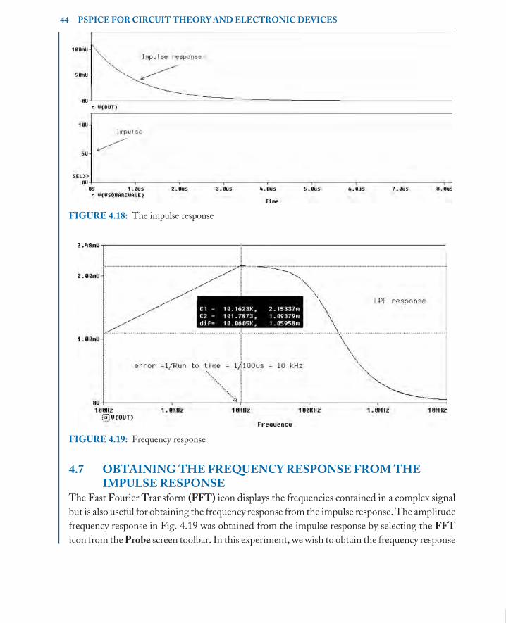
book Mobk059 March 9, 2007 10:21
44 PSPICE FOR CIRCUIT THEORY AND ELECTRONIC DEVICES
FIGURE 4.18: The impulse response
FIGURE 4.19: Frequency response
4.7 OBTAINING THE FREQUENCY RESPONSE FROM THEIMPULSE RESPONSE
The Fast Fourier Transform (FFT) icon displays the frequencies contained in a complex signal
but is also useful for obtaining the frequency response from the impulse response. The amplitude
frequency response in Fig. 4.19 was obtained from the impulse response by selecting the FFT
icon from the Probe screen toolbar. In this experiment, we wish to obtain the frequency response
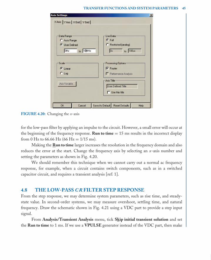
book Mobk059 March 9, 2007 10:21
TRANSFER FUNCTIONS AND SYSTEM PARAMETERS 45
FIGURE 4.20: Changing the x-axis
for the low-pass filter by applying an impulse to the circuit. However, a small error will occur at
the beginning of the frequency response. Run to time = 15 ms results in the incorrect display
from 0 Hz to 66.66 Hz (66 Hz = 1/15 ms).
Making the Run to time larger increases the resolution in the frequency domain and also
reduces the error at the start. Change the frequency axis by selecting an x-axis number and
setting the parameters as shown in Fig. 4.20.
We should remember this technique when we cannot carry out a normal ac frequency
response, for example, when a circuit contains switch components, such as in a switched
capacitor circuit, and requires a transient analysis [ref: 1].
4.8 THE LOW-PASS C R FILTER STEP RESPONSEFrom the step response, we may determine system parameters, such as rise time, and steady-
state value. In second-order systems, we may measure overshoot, settling time, and natural
frequency. Draw the schematic shown in Fig. 4.21 using a VDC part to provide a step input
signal.
From Analysis/Transient Analysis menu, tick Skip initial transient solution and set
the Run to time to 1 ms. If we use a VPULSE generator instead of the VDC part, then make
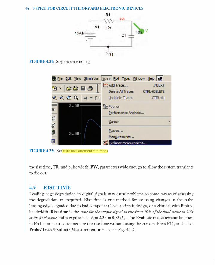
book Mobk059 March 9, 2007 10:21
46 PSPICE FOR CIRCUIT THEORY AND ELECTRONIC DEVICES
FIGURE 4.21: Step response testing
FIGURE 4.22: Evaluate measurement functions
the rise time, TR, and pulse width, PW, parameters wide enough to allow the system transients
to die out.
4.9 RISE TIMELeading-edge degradation in digital signals may cause problems so some means of assessing
the degradation are required. Rise time is one method for assessing changes in the pulse
leading edge degraded due to bad component layout, circuit design, or a channel with limited
bandwidth. Rise time is the time for the output signal to rise from 10% of the final value to 90%
of the final value and is expressed as tr = 2.2τ = 0.35/f c . The Evaluate measurement function
in Probe can be used to measure the rise time without using the cursors. Press F11, and select
Probe/Trace/Evaluate Measurement menu as in Fig. 4.22.

book Mobk059 March 9, 2007 10:21
TRANSFER FUNCTIONS AND SYSTEM PARAMETERS 47
FIGURE 4.23: Evaluate measurement functions
FIGURE 4.24: Rise-time measurement using Evaluate Measurement function
Select Risetime (1) from the list of functions in Fig. 4.23 to place it in the Trace
Expression box.
Replace the default “1” value in the function brackets with the capacitor voltage V(out)
function, selected from the list on the left. Fig. 4.24 shows the Evaluate Measurement function
evaluated at the bottom as 10% final value to 90% final value equal to tr = 2.2τ = 2.2 C R =
2.2∗1e4∗10e − 9 = 219 us.

book Mobk059 March 9, 2007 10:21
48 PSPICE FOR CIRCUIT THEORY AND ELECTRONIC DEVICES
FIGURE 4.25: Second-order LCR circuit
4.10 STEP RESPONSE OF A SERIES-TUNED LCR CIRCUITThe second-order resonant LCR circuit in Fig. 4.25 investigates “circuit damping” by varying
the circuit resistance and observing the waveforms. Select the resistance and change the default
1 k� to {Rvar} (brackets included).
A PARAM part defines Name1 = RVAR for the resistance, and Value1 = 1. From the
Analysis Setup menu, select Parametric, and set Name to RVAR. Set Start Value = 20 �,
End Value = 200 � and a 60 � resistance increment. Set the Analysis tab to Analysis type:
Time Domain (Transient), Run to time = 15 ms, and Maximum step size = 1 us. After
pressing F11 to simulate, a small screen of Available Sections will appear, so select OK, or
press the ENTER button. The range of damping from underdamped to overdamp is shown in
the step response in Fig. 4.26.
4.10.1 OvershootOvershoot is a measure of the step response of a circuit. When a circuit is underdamped
the output rises to a maximum of 1.38 V, an excess of 0.38 V for a 1 V step. Use the
Probe/Trace/Evaluate Measurement Functions in Probe to measure all parameters. For
example, the overshoot function: Overshoot(V(C1:2)), yields an over shoot of 38% as shown at
the bottom of Fig. 4.26. You should also notice at the bottom of the display symbols representing
each trace. Selecting any one of these symbols shows the information for a particular value of
the swept variable.
4.11 EXERCISES(1) Use an ABM E part to create the integrator in Fig. 4.27. The input data is applied
using a VPWL part, or a VPULSE part with ±1 V amplitude, PW =1 ns, and PER
= 2 n. Here, τ = CR = 1 k� × 2 pF = 2 ns.
(2) An oscilloscope probe reduces the effect of the input oscilloscope capacitance on a
signal. Without such a probe, a step or pulse signal has the rise time degraded. The
10:1 oscilloscope probe in Fig. 4.28 is calibrated by attaching the probe end onto the

book Mobk059 March 9, 2007 10:21
TRANSFER FUNCTIONS AND SYSTEM PARAMETERS 49
FIGURE 4.26: Range of damping coefficients
FIGURE 4.27: Integration using the E part
reference square wave signal on the front panel of the oscilloscope. In normal usage,
the probe tip variable capacitance is adjusted by inserting a small plastic trimming
tool and adjusting it to produce the best displayed square wave. The best display is
where the applied signal looks like the original reference but reduced in amplitude by a
factor of 10.
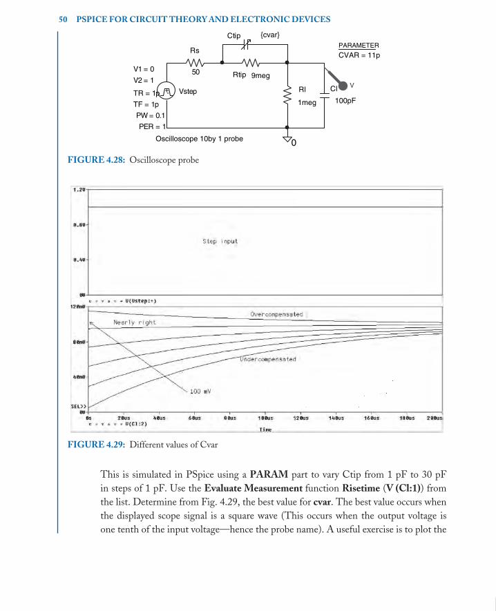
book Mobk059 March 9, 2007 10:21
50 PSPICE FOR CIRCUIT THEORY AND ELECTRONIC DEVICES
Rl
1meg
Rs
50
Vstep
V1 = 0
V2 = 1
TR = 1p
TF = 1p
PER = 1
PW = 0.1
+-
PARAMETER
CVAR = 11p
Rtip 9meg
Ctip {cvar}
Cl
100pF
0Oscilloscope 10by 1 probe
V
FIGURE 4.28: Oscilloscope probe
FIGURE 4.29: Different values of Cvar
This is simulated in PSpice using a PARAM part to vary Ctip from 1 pF to 30 pF
in steps of 1 pF. Use the Evaluate Measurement function Risetime (V (Cl:1)) from
the list. Determine from Fig. 4.29, the best value for cvar. The best value occurs when
the displayed scope signal is a square wave (This occurs when the output voltage is
one tenth of the input voltage—hence the probe name). A useful exercise is to plot the
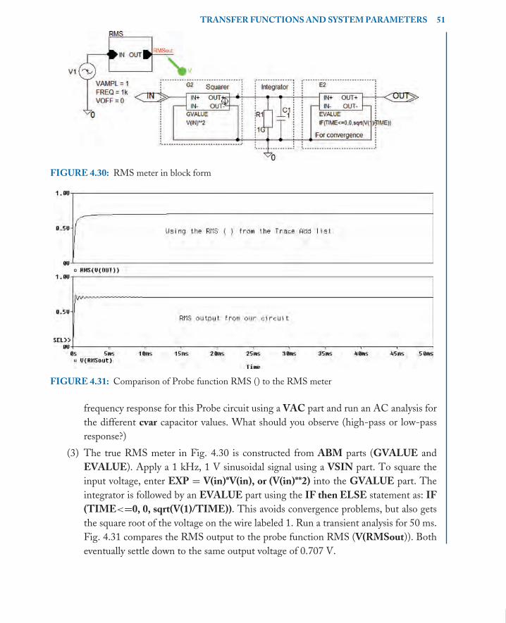
book Mobk059 March 9, 2007 10:21
TRANSFER FUNCTIONS AND SYSTEM PARAMETERS 51
FIGURE 4.30: RMS meter in block form
FIGURE 4.31: Comparison of Probe function RMS () to the RMS meter
frequency response for this Probe circuit using a VAC part and run an AC analysis for
the different cvar capacitor values. What should you observe (high-pass or low-pass
response?)
(3) The true RMS meter in Fig. 4.30 is constructed from ABM parts (GVALUE and
EVALUE). Apply a 1 kHz, 1 V sinusoidal signal using a VSIN part. To square the
input voltage, enter EXP = V(in)*V(in), or (V(in)**2) into the GVALUE part. The
integrator is followed by an EVALUE part using the IF then ELSE statement as: IF
(TIME<=0, 0, sqrt(V(1)/TIME)). This avoids convergence problems, but also gets
the square root of the voltage on the wire labeled 1. Run a transient analysis for 50 ms.
Fig. 4.31 compares the RMS output to the probe function RMS (V(RMSout)). Both
eventually settle down to the same output voltage of 0.707 V.