publications in - dtic.mil troll silicon. preface ... 95-percent confidence level on the tation ......
TRANSCRIPT

SEMICONDIATOR TECHNOLOGY PROGRAM ABSTRACT - This report provides informationon the current status of NBS work on mea-
TABLE OF CONTENTS surement technology for semiconductor mate-rials, process control, and devices. Empha-
sis is placed on silicon and silicon-basedSilicon Resistivity SRMs.. ......... devices. Highlighted activities includeDeep-Level Measurements . ........ . 3 newly issued resistivity SRMs, characteris-
Photoluminescence Studies............ tics of sulfur-related deep levels in sili-con, photoluminescence of Indium-doped sili-
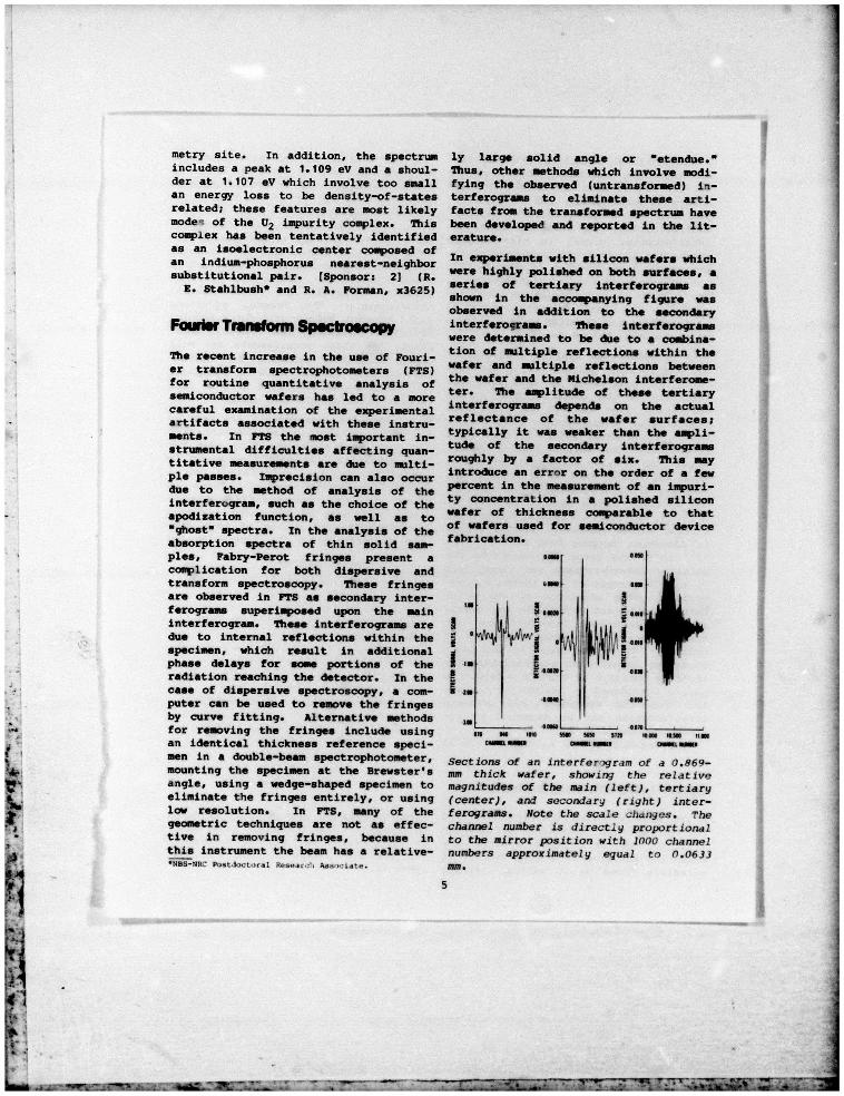
Fourier Transform Spectroscopy ...... 5 con, effect of tertiary interferograms onFourier transform spectroscopy, design in-formation for a set of wafer optical line-
Linewidth Measurement Seminars ..... .. 7 width standards, modeling of short-channelMOS transistors, acoustic-emission testing
Device Modelng................... 7 of tape-bonded IC9, laser scanning of a
Acoustic-Emission Testing ...... . a solar cell test pattern, power loss of tran-sistor leads during fast switching, and
Production Bond Tester for TAB ICs . . . 9 itrlasdin fst wtcng ad
Ssecond breakdown and radiation effects inSolar Cell Measurement Techniques . . . 10 power MOS transistors. Brief descriptions
of an upcoming linewidth measurement seminarand a survey of Federal IC processing facil-
Second Breakdown in Power MOSFETs . . . 11 ities are given. In addition, recent publi-cations and publications in press are
Radiation Effects on Power MOSFET9 . . . 12 c in n ulctosI rs rlisted. The report is not meant to be ex-
Federal IC Processing Facilities . ... 12 haustive; contacts for obtaining furtherinformation are listed.
Recent Publications . .......... 3
Publications in Press........... .14 KEY WORDS - Electronics; integrated cir-cuits, measurement technology; microelec-tronics; semiconductor devices, semiconduc-tor materials; semiconductor process con-troll silicon.
Preface
This report covers results of work during the fifty-first quarter of the NBS SemiconductorTechnology Program. This Program serves to focus NBS research on improved measurementtechnology for the use of the semiconductor device community in specifying materials,equipment, and devices in national and international commerce, and in monitoring and con-trolling device fabrication and assembly. This research leads to carefully evaluated,well-documented test procedures and associated technology which, when applied by the indus-try, are expected to contribute to higher yields, lower cost, and higher reliability of
semiconductor devices and to provide a basis for controlled improvements in fabrication
processes and device performance. By providing a common basis for the purchase specifica-tions of government agencies, improved measurement technology also leads to greater economyin government procurement. Financial support of the Program is provided by a variety ofFederal agencies. The sponsor of each technical project is identified at the end of eachentry in accordance with the following code: 1. The Defense Advanced Research ProjectsAgency; 2. The National Bureau of Standards; 3. The Division of Electric Energy System,Department of Energy; 5. The Defense Nuclear Agency, 6. The C. S. Draper Laboratory 10.The Naval Weapons Support Center; 11. The Solar Energy Research Institute; 12. The Naval*Avionics Center; 13. The Lewis Research Center, National Aeronautics and Space Administra-tion; and 15. The Naval Ocean Systems Center.
This report is provided to disseminate results rapidly to the semiconductor commnity. Itis not meant to be complete; in particular, references to prior work either at NUS orelsewhere are omitted. The Program is a continuing oner the results and conclusions re-ported herein are subject to modification and refinement. fZ urther information may be ob-
R tained by referring to more formal technical pvblicatiohsi or directly from responsiblestaff members, telephone: (301) 921-listed extension. General information, past issues ofprogress briefs, and a list of publications may be obtained from the Electron Devices Divi-sion, National Bureau of Standards, Washington, D.C. 20234, telephone: (301) 921-3786.
2
AA
Semiconductor Technology ProgramProgress Briefs
Silicon Resistivity SRMs Deep-Level MeasurementsA new silicon resistivity SRM is now Additional electrical evidence has beenavailable from the NBS Office of Stan- obtained which confirms the complexdard Reference Materials (OSRM). This nature of sulfur-related deep levels inSRM, designated SRM 1523, Silicon Resis- silicon. One would expect that thetivity Standard for Eddy Current Test- thermal emission rate from a singleers, is designed primarily for use with physical defect species in silicon would"contactless" resistivity testers; it is be a well-defined, reproducible functionalso suitable for use with four-probe of the temperature of the test specimen.instruments. It contains two boron- Examination of the effect of a varietydoped silicon slices, one each at nomi- of experimental factors on the thermalnal resistivities of 0.01 and 1 0.cm. emission rate from sulfur-related cen-The slices are nominally 2 in. (51 mm) ters in silicon revealed that the ratein diameter and 0.63 nun thick; they were varies with virtually every experimentalcut from (100) Czochralski and (111) parameter studied.float-zone-grown crystals, respectively. Deep-level transient spectroscopy (DLTS)The resistivity of each slice was indi- measurements were made on six siliconvidually measured by the four-probe wafers into which sulfur had been intro-technique using ASTM Method F 84. The duced in varying amounts by ion implan-95-percent confidence level on the tation (and subsequent redistribution atstated resistivity values is ±2.5 per- 1000C). At low sulfur density, thecent of those values. This confidence spectrum exhibits two sulfur-relatedvalue is a conservative statement re- peaks of about the same amplitude. Assulting from a two-instrument, two- the sulfur density increases, the ampli-operator experiment at NES. tude of the lower temperature peak in-
This SRM supplements the values of sili- creases more rapidly than that of thecon resistivity standards which are higher temperature peak. In addition,available in two other previously an- the positions of these peaks shift andnounced SRMs. Supplies of these SRMs other peaks appear in the spectrum.have recently been replenished; both are Differences from the spectra of thesenow available from the OSRM. SRM 1521 ion-implanted specimens are also ob-contains two slices of (111) float-zone- served in the DLTS spectrum of a silicongrown, boron-doped silicon at nominal wafer into which the sulfur was intro-resistivities of 0.1 and 10 0.cm. SRM duced by diffusion in a sealed quartz1522 contains three slices of (111) tube at 1350*C.silicon doped with phosphorus by the More precise determination of the ther-neutron transmutation process to nominal mal emission rate is possible with theresistivities of 25, 75, and 180 0.cm.
use of the isothermal transient capaci-tance (ITCAP) method. Differences, suchalso nominally 2 in. in diameter and0.63 mm thick, each has been individual- as a il sred in the acmpanlyfigure, are observed in the time con-stant of the capacitance transient be-
N. The price for SRM 1523 is $300, and the fore and after a thermal anneal. Theprices for SRM 1521 and 1522 are $300 figure shows the capacitance of theand $425, respectively. [Sponsor: 2] depletion layer as a function of time,
(J. R. Ehrstein, x3625) starting from before the trap-filling
3
t I
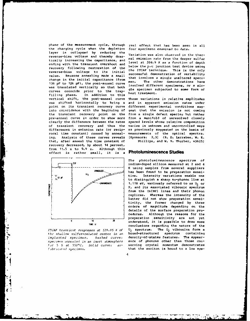
phase of the measurement cycle, through real effect that has been seen in all
the charging cycle when the depletion four specimens examined to date.layer is collapsed by reducing theyersis olasend by dras-ing theVariation was also observed in the ther-ticarsy-inceasinglte caatanee, d- mal emission rate from the deeper sulfurtically increasing the capacitance, and level at 204.9 K as a function of depthending with the transient overshoot and b l w t e p n j n t o e t d v c s nrecoeryfolowig retortio ofthebelow the p-nz junction test device usingrecovery following restoration ofit the ITCAP technique. This is the onlyrver ease voaeai mae as snal successful demonstration of variabilityvalu. Bcaue anealng adea sallthat involves a single unaltered speci-change in the initial capacitance (from that involve a emunatred spe136 pF to 126 pF), the post-anneal curve involved different specimens, or a sin-was translated vertically so that both gle specimen subjected to some form ofcurves coincide prior to the trap- heat treatment.filling phase. In addition to thisvertical shift, the post-anneal curve These variations in relative amplitudeswas shifted horizontally to bring a and in apparent emission rates underpoint on its transient recovery curve different experimental conditions sug-into coincidence with the beginning of gest that the emission is not comingthe transient recovery point on the from a single defect species but ratherpre-anneal curve in order to show more from a manifold of unresolved closelyclearly the difference between the rates spaced levels whose relative compositionof transient recovery and thus the varies in unknown and uncontrolled waysdifferences in emission rate (or recip- as previously suggested on the basis ofrocal time constant) caused by anneal- measurements of the optical spectra.ing. Analysis of these curves reveals [Sponsors: 2,3] (R. D. Larrabee, W. E.that, after anneal the time constant of Phillips, and W. R. Thurber, x3625)recovery decreased, by about 14 percent,from 11.5 s to 9.9 s. Although thiseffect is rather small, it is a Photoluminescence Studies
The photoluminescence spectrum of---- C01 indium-doped silicon measured at 2 and 4
Cf . ----- ---------------------------- K using samples from several suppliersANNALED.. has been found to be preparation sensi-
US_T0 I - tive. Intensity variations enable one
IO to distinguish a sharp no-phonon line at-UNANNALED 1.118 eV, variously referred to as U2 or
I .P, and its associated vibronic spectrumfrom the In(NP) lines and their phonon
I replicas. Whereas the intensity of thelatter did not show preparation sensi-tivity, the former changed by threeorders of magnitude depending on thedetails of the surface preparation pro-cedures. Although the reasons for thepreparation sensitivity are not yet
10 understood, it is possible to draw someTINsW conclusions regarding the nature of the
ITCAP transient responses at 129.95 K of U2 spectrum. The U2 vibronics form athe shallow sulfur-related center in an broad-structured spectrum containingimplanted specimen. Dashed curve: density-of-states features. The appear-specimen dnnealel in an inert atmosphere ance of phonons other than those con-for 5 h at 550°C. Solid curve: as- serving crystal momentum demonstratesf-ibricated specimen, that the exciton is bound to a low sym-
- 4
,I
-. i.............................................................................. I
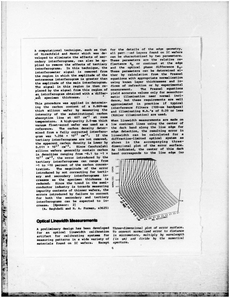

error) only along the axis where RO = materials if multilayer substrates are1. As the contrast at the line edge used.increases CR0 < 1.0), the error in Plans are underway to fabricate such alinewidth increases, scaling with wave- set of wafer materials and test thislength of the illumination and inversely method of calibration on commerciallywith the N.A. of the objective. Because available linewidth measurement systems.of the predictable behavior of thiskown ysthe aicabl er ir o tis For other edge-detection criteria, anknown systematic error, it is possible optimum set of Rm , Om values may beto calibrate such a system using far oimum seteofined.m[valus m bfewer pairs of values of Ro and 00 similarly determined. [sponsor: 21than would normally be required to char- (D. Nyyssonen, x3621)acterize an unknown error surface. Forthe case illustrated, a third-order LinewidthMeasurementSeminarspolynomial can be used for calibration,and only five combinations of R. and#oare required to characterize the A 3-day training seminar on Linewidth
Measurements on Integrated Circuit Pho-error surface. Some possible choices tomasks and Wafers is to be held in theare shown in the accompanying plot of Washington, D.C. area on November 18-20,the Ro- o plane. The optimum coor- 1981, to present up-to-date informationdinates (Rm, 0m) are determined by on the accurate measurement of line-application of Gauss-quadrature formu- widths in the 0.5- to 10-ur range. Thelas. These formulas have been developed seminar includes lecture sessions,for simple square and circular regions.Mapingof heknon otimm oorinaesequipment demonstrations, and groupMapping of the known optimum coordinates discussions. Emphasis is on opticalfor a square region onto the indicatedtrapezoid produces the families of microscope techniques. The 75-person
points shown on the plot. Several of capacity of this seminar is expected to
the points shown correspond to patterned be oversubscribed; a similar seminar issingle layers of oxide or nitride on tentatively scheduled to be held in thesiliongle laye pars of e or nSouthwest in the fall of 1982. [Spon-silicon. Other pairs of Rm ,
4 m sor: 21 (E. C.
values can be produced from a variety of ohn 21 aE. C.Cohen, x3786, and J. M. Jerke, x3621)
Device Modeling... The two-dimensional charge-sheet model
$ a" ,for short-channel MOS transistors was_extended to transistors of channel
- - length down to 1 tim. The model is for--, " "- mulated to include the effect of channel
C inversion layer charge as a nonlinear" * integral boundary condition on the two-
dimensional electrostatic fields in thetransistor. This formulation allows the
e odrain current and electrostatic poten-View of the se, 1, plane showing tial to be computed simultaneously with-
Ssets of points (set 1, *; set 2, 0) out including the full electron currentSwhich can be used] to calibrate the ou inldgth fllecrncret
continuity equation. This simplifica-shaded trapezoidaC region. Curves cor- tion results in significant increases inrespond to layers with incredsing indi- computational efficiency.
ces of refraction: A) silicon dioxideon silicon (n 1.46), B) nitrided Sio 2 The simulations produced using thison silicon (n 1.6), and C) Si3N4 de- model have been compared with experimen-
54 posited by LPCVD (n 1.98). tal measurements. Although some conver-
vJ"I
i-
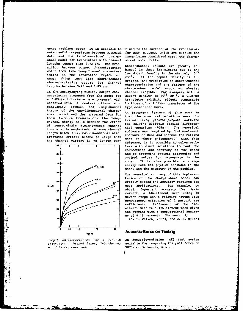
gence problems occur, it is possible to fined to the surface of the transistor;make useful comparisons between measured for such devices, which are outside thedata and the two-dimensional charge- range being considered here, the charge-sheet model for transistors with channel sheet model fails.lengths longer than 1.12 jim. The tran- Short-channel effects are greatly en-sition between output characteristics hanced in these transistors due to thewhich look like long-channel character- low dopant density in the channel, 1015istics in the saturation region and 3those which look like short-channel cm- 3 . If the dopant density is in-characteristics occurs for channel creased, the transition to short-channel
characteristics and the failure of thelengths between 3.20 and 1.89 jrn, charge-sheet model occur at shorter
In the accompanying figure, output char- channel lengths. For example, with aacteristics computed from the model for dopant density of 1016 cm- , a 0.35-Mma 1.89-trm transistor are compared with transistor exhibits effects comparablemeasured data. In contrast, there is no to those of a 1.12-Um transistor of thesimilarity between the long-channel type described here.theory of the one-dimensional charge- An important feature of this work issheet model and the measured data for that the numerical solutions were ob-this 1.89-ijm transistor; the long- tained using general-purpose softwarechannel theory fails because the effect ao gerarpose sftwrefor solving elliptic partial differen-of source-drain field-induced channel tial equations (PDEB). The numericalinversion is neglected. At some channel software was inspired by finite-elementlength below I pm, two-dimensional elec- software of Bank and Sherman and retainstrostatic effects become so large that most of their philosophy. With thisthe channel current is no longer con- software, it is possible to solve prob-
mI I I lems with exact solutions to test the
correctness and accuracy of the codesand to determine optimal strategies andoptimal values for parameters in thecode. It is also possible to change
7t- easily both the physics included in themodel and the geometry of the problem.
'- The numerical accuracy of this implemen-
tation of the charge-sheet model can- - greatly exceed the accuracy required for
lIuD .,. most applications. For example, to40 - obtain 5-percent accuracy for drain
current, a 146-element mesh using 10v Newton steps and a relative Newton step
3M convergence criterion of 2 percent are.. sufficient. Refinement of the 146-
- element mesh to a 455-element mesh givesthe current with a computational accura-cy of 0.16 percent. [Sponsor: 2]
, ' (C. L. Wilson, x3621, and J. L. Blue*)
i i
Acoustic-Emission Testing
3Ofutpuit chardcteristics for a l.R9-pm An acoustic-emission (AE) test systemtransistor. Dashed Iines, 2-D theory; suitable for comparing the pull force orsoi 1 lines, measured. , Computq Divion.
4If,
--- -

the flexure fatigue strength of differ- that of the unplated TC-bonded leads.ent alloy leads or the susceptibility of Thus, it is concluded that the gold-tin-surface platings to crack or to separate copper alloy had embrittled the lead atduring flexure was developed. It has the edge of the bump. The implicationbeen applied to tape-bonded (TAB) inte- is that if TAB devices are to be ingrated circuit leads and package lead plastic-encapsulated packages, the un-frames. In use, an individual bonded plated copper would best withstand ther-lead is clamped by a microtweezer and is mal cycling environments such as thosepulled or vibrated at a frequency of encountered in automotive applications.between 10 and 100 Hz, and the acoustic TAB devices from one manufacturer's lotemission is monitored. Power for the in each tape size were available forvibration solenoid is passed through an these tests. The purity and hardness ofelectronic switch which is turned off by the leads were not known, so it is pos-the acoustic-emission trigger unit when sible that other similar TAB leads maya bond begins to lift, lead fatigue show better fatigue strength. However,cracks propagate, or the lead plating considering the factor of ten differenceseparates. in microfatigue strength, it appears
desirable to conduct fatigue tests whenLead vibration tests were carried out to determiln th lond ig pete
compare the fatigue characteristics of determining the lead-bonding parameters
11-mm all-copper tape with thermocom- (time, temperature, and force) as wellas finished device suitability for en-
pression (TC)-bonded copper leads and asuin aduse iaet evron-
35-mm polyimide-based tape with tin- capsulation and use in extreme environ-
plated copper leads, melt-bonded to gold ments. [Sponsor: 21
bumps. Such tests were usually carried (G. G. Harman, x3621)
out with a constant upward pull force of50 mN and a vibration force of ±9.8 mNat 40 Hz. The microtweezer hook clamped Production Bond Tester for TAB ICsthe lead approximately 0.015 cm out fromthe chip. In all cases, the tin-plated A prototype automatic tester has beenleads on the 35-mm format broke within 1 designed for production monitoring ofto 2 s at the edge of the bump (40 to 80 the bond quality of tape-bonded inte-vibration cycles), whereas the unplated grated circuits. In operation, the tapeTC-bonded leads of the 11-mm tape with- is advanced until the chip is centeredstood at least 10 times as many vibra- in the fixture. A tool clamps the chiption cycles before breaking at the edge by pressing down on top of the bonds onof the bump. Only a few prebreak AE two opposite sides of the chip. Anotherbursts were recorded for either type of tool rises from below, exerts a verticallead. However, since a totalizer which lifting force against the unclampedprints AE data once each second was used leads, and bends them upward. Thefor data analysis, it is possible that acoustic emission (AE) resulting fromprebreak bursts occurred within the this stress is monitored. The forcefinal second and were not separated from~ applied to the leads is dependent on howAE generated during the break, close the tool is to the edge of the
It was concluded that the combination of chip. The desired test force is experi-
tin plating and alloy bonding resulted mentally determined for each device typein a much more brittle bond heel than or lead design, but is on the order ofthat of the TC-bonded unplated copper 100 mN per lead. The clamp force isthat o Thes Tas-bondied unp at n copp then released, both tools are rotated 90leads. This was verified by fatiguing deg, and the remaining bonds are tested.the tin-plated leads at their tape in-terface where no gold-tin alloy was Both a trigger unit and a totalizerpresent. The fatigue strength of this which cumulates all AE events above aend of the lead (including corrections preset threshold each second are used tofor increased line width) was as high as assist in the interpretation of fail-
9
4
~~~~~~~~~~-- --- -- -- -- ------..- ----.-----," ... • , -' l : ...- -i III i , ,