push-pull integrate-optics mach-zehnder interferometer with domain inversion in one branch
TRANSCRIPT

288 OPTICS LETTERS / Vol. 20, No. 3 / February 1, 1995
Push–pull integrated-optics Mach–Zehnder interferometerwith domain inversion in one branch
Nicolas A. F. Jaeger and Lisheng Huang*Department of Electrical Engineering, University of British Columbia, Vancouver, British Columbia V6T 1Z4, Canada
Received July 15, 1994
We report on a push–pull integrated-optics Mach–Zehnder interferometer having one domain-inverted branchand one noninverted branch. It is fabricated in the c1 side of a LiNbO3 substrate. We achieve ferroelectricdomain inversion in one branch of the waveguide by doping it more heavily with Ti than the other branch and byusing a high-temperature treatment that raises the temperature above the doped Curie temperature of the onebranch but not of the other. The cumulative electro-optic effect of the inverted branch is found to be oppositethat in the noninverted branch when both are subjected to the same electric field.
Lithium niobate (LiNbO3) has been widely used forintegrated-optical device fabrication because of itsuseful electro-optic, acoustic, and photorefractiveproperties.1 – 3 Also, techniques for fabricating op-tical waveguides in LiNbO3, with both Ti indiffusionand proton exchange, are well developed.4 To uti-lize the large r33 electro-optic coefficient, many de-vices are designed to have the electric field appliedparallel to the c axis.
One of the problems that is encountered in c-cutsubstrates is ferroelectric domain inversion on the c1
side, resulting from the high temperature at which Tiis indiffused. This degrades the electro-optic effectof the material and hence the performance of thedevice.5,6 Therefore, the c2 side of LiNbO3 is usuallypreferred for the fabrication of devices.
An inverted domain has its spontaneous polar-ization oriented in the direction opposite that ina noninverted domain. Some researchers havebeen utilizing inverted domains in the designs ofnew devices, e.g., piezoelectric resonators andacoustic transducers,7 or to obtain domain-invertedchannels for second-harmonic generation.8 – 10 Al-though Sriram et al. proposed using domain inver-sion to make electric-field sensors,11 and Schaffnerhas proposed using periodic domain-inverted wave-guides to make quasi-phase-matched high-speed op-tical modulators,12 we have not found any studiesdescribing working devices of these types; there-fore, here we report on such a Mach–Zehnder in-terferometer with domain inversion in one of thebranches. By achieving inversion in one branch,the Mach–Zehnder interferometer can be used in apush–pull fashion when both branches are subjectedto the same electric field.
The goal of the device design was to invert theferroelectric domains in a specific region throughwhich one of the two branches of the Mach–Zehnderinterferometer passed. The electro-optic response inthe domain-inverted region would be, therefore, op-posite that in the rest of crystal. As was shown inRef. 5, it is possible to obtain a fully inverted re-gion by use of high Ti dopant levels; this occurs be-cause the Ti indiffusion lowers the Curie temperaturein such a region. It is well known that the Curie
0146-9592/95/030288-03$6.00/0
temperature of Ti-doped LiNbO3 (Tc0) decreases as
the Ti concentration increases.4,5,13 We can, there-fore, try to use a Ti indiffusion with a high dopinglevel to lower Tc
0 to achieve domain inversion in onebranch, but not in the other branch, when the sampleis heated to a specific temperature.
We used the data of Guenais et al.13 to obtain thequantitative relation Tc
0 1141 2 1076x (±C) be-tween the doped Curie temperature and the molefraction in the system LiNbO3: xTiO2; 1141 ±C is theCurie temperature of congruent LiNbO3.13,14 In ourdevice we modeled the postdiffusion Ti concentrationprofile by a Gaussian function in the depth direc-tion and complimentary error functions in the lat-eral direction.15 The mole fraction of TiO2 can beestimated with the help of the calibration curves ofMinakata et al.16 The above relation allows one toobtain fabrication parameters giving the desired do-main inversion. In our case we wanted to achievethe maximum inversion possible in one branch andno inversion in the other.
The Tc0 profiles were calculated for two diffusion
processes, one for each of the two branches of aMach–Zehnder interferometer. Process A involvedthe indiffusion of a 100-nm-thick, 3.5-mm-wide ini-tial Ti strip at 1050 ±C for 10 h followed by the indiffu-sion of a 40-nm-thick, 3.5-mm-wide Ti strip at 1050 ±Cfor 6.25 h. Process B involved only the indiffusionof a 40-nm-thick, 3.5-mm-wide Ti strip at 1050 ±Cfor 6.25 h. The resulting Tc
0 profiles are depicted inFigs. 1 and 2 by solid curves for process A and bydashed curves for process B. Figure 1 shows the Tc
0
profiles in the lateral direction at the surface of thesample, and Fig. 2 shows the Tc
0 profiles in the depthdirection at the centers of the waveguides. It can beseen from the solid curves that a 1100 ±C heat treat-ment should result in an inverted region approxi-mately 5 mm wide and 2 mm deep for the branchfabricated by process A, assuming complete domaininversion in the region where Tc
0 , 1100 ±C. It canalso be seen that the minimum Tc
0 for the dashedcurves is 1121 ±C and that no inversion is expected inthe branch fabricated by process B for the same heattreatment.
Our Mach–Zehnder interferometers were fabri-
1995 Optical Society of America
February 1, 1995 / Vol. 20, No. 3 / OPTICS LETTERS 289
Fig. 1. Lateral profiles for Tc0 at the surface of the
sample resulting from process A (solid curve) and processB (dashed curve).
Fig. 2. Depth profiles for Tc0 at the center of the wave-
guide resulting from process A (solid curve) and processB (dashed curve).
cated on the c1 surfaces of LiNbO3 substrates. Lift-off lithography was used to pattern the initial Tistrips (100 nm thick, 3.5 mm wide, and 10 mm long).They were indiffused at 1050 ±C for 10 h with O2
bubbling through deionized water.17 The substrateswere covered with another piece of LiNbO3 to reduceLi outdiffusion.
After diffusion of the initial Ti strips, the Mach–Zehnder interferometer waveguides were patternedin such a way that one branch was aligned over theinitial strip, parallel to its length, whereas the otherbranch was far away, 20 mm, from the strip. Thewidth of the Ti used to define the Mach–Zehnderwaveguides before diffusion was 3.5 mm, and thethickness was ,40 nm. This Ti waveguide patternwas indiffused, again with O2 bubbled through deion-ized water, at 1050 ±C for 6.25 h; here too the sub-strates were covered with another piece of LiNbO3.The temperature was then increased to 1100 ±C for15 min. After the diffusion and the heat treatment,the sample was cooled, a SiO2 optical buffer layer was
sputter-deposited onto the surface containing theMach–Zehnder interferometer, and Al was evapo-rated onto both the c1 and c2 faces of the wafer,forming parallel plate electrodes.
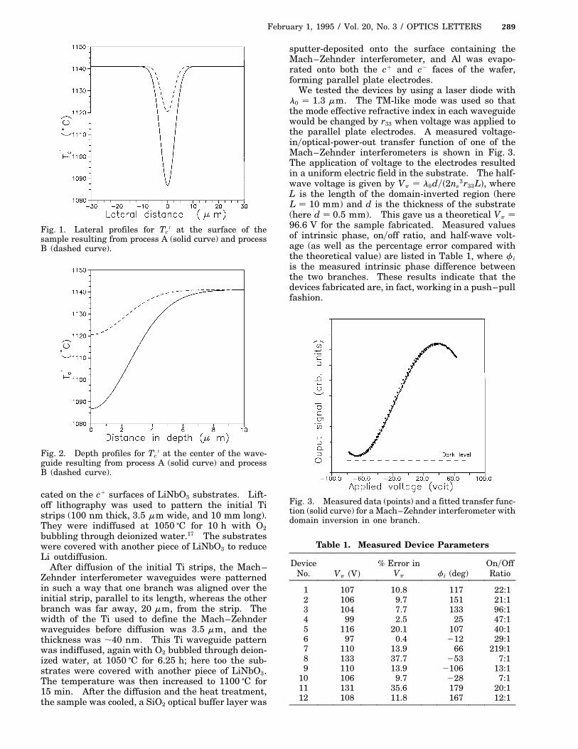
We tested the devices by using a laser diode withl0 1.3 mm. The TM-like mode was used so thatthe mode effective refractive index in each waveguidewould be changed by r33 when voltage was applied tothe parallel plate electrodes. A measured voltage-inyoptical-power-out transfer function of one of theMach–Zehnder interferometers is shown in Fig. 3.The application of voltage to the electrodes resultedin a uniform electric field in the substrate. The half-wave voltage is given by Vp l0dys2ne
3r33Ld, whereL is the length of the domain-inverted region (hereL 10 mm) and d is the thickness of the substrate(here d 0.5 mm). This gave us a theoretical Vp 96.6 V for the sample fabricated. Measured valuesof intrinsic phase, onyoff ratio, and half-wave volt-age (as well as the percentage error compared withthe theoretical value) are listed in Table 1, where fi
is the measured intrinsic phase difference betweenthe two branches. These results indicate that thedevices fabricated are, in fact, working in a push–pullfashion.
Fig. 3. Measured data (points) and a fitted transfer func-tion (solid curve) for a Mach–Zehnder interferometer withdomain inversion in one branch.
Table 1. Measured Device Parameters
Device % Error in OnyOffNo. Vp sV d Vp fi (deg) Ratio
1 107 10.8 117 22:12 106 9.7 151 21:13 104 7.7 133 96:14 99 2.5 25 47:15 116 20.1 107 40:16 97 0.4 212 29:17 110 13.9 66 219:18 133 37.7 253 7:19 110 13.9 2106 13:1
10 106 9.7 228 7:111 131 35.6 179 20:112 108 11.8 167 12:1

290 OPTICS LETTERS / Vol. 20, No. 3 / February 1, 1995
In summary, we have fabricated a push–pullMach–Zehnder interferometer in LiNbO3 in whichthe push–pull effect is realized by selectively achiev-ing domain inversion in one branch of the devicewhile leaving the other branch unaffected.
This research was supported by grants from theScience Council of British Columbia and the Natu-ral Sciences and Engineering Research Council ofCanada.
*Present address, National Optics Institute, 369rue Franquet, Sainte-Foy, Quebec G1P 4N8, Canada.
Note added in proof: At the time we submittedthis Letter the paper by Naghski et al.,18 describinga similar device, was not available.
References
1. Properties of Lithium Niobate, EMIS Data ReviewsSeries No. 5 (Institution of Electrical Engineers,London, 1989).
2. T. Tamir, ed., Guided-Wave Optoelectronics (Springer-Verlag, Berlin, 1990).
3. I. Kaminow, Introduction to Electro-optic Devices (Aca-demic, New York, 1974).
4. M. N. Armenise, Proc. Inst. Electr. Eng. 85, 135(1988).
5. S. Miyazawa, J. Appl. Phys. 50, 4599 (1979).6. S. Thaniyavarn, T. Findkly, D. Booher, and J. Moen,
Appl. Phys. Lett. 46, 933 (1985).7. K. Nakamura, H. Ando, and H. Shimizu, Appl. Phys.
Lett. 50, 1413 (1987).8. J. Webjorn, F. Laurell, and G. Arvidsson, J. Lightwave
Technol. 7, 1597 (1989).9. E. J. Lim, M. M. Fejer, and R. L. Byer, Electron. Lett.
25, 174 (1989).10. K. Kawano, T. Kitoh, H. Jumonji, T. Nozawa, and M.
Yanagibashi, Electron. Lett. 25, 1382 (1989).11. S. S. Sriram, S. A. Kingsley, and J. T. Boyd, U.S.
patent 5,267,336 (November 30, 1993).12. J. H. Schaffner, U.S. patent 5,278,924 (January 11,
1994).13. B. Guenais, M. Baudet, M. Minier, and M. Le Cun,
Mater. Res. Bull. 16, 643 (1981).14. S. C. Abrahams and P. Marsh, Acta Crystallogr. B 42,
61 (1986).15. S. K. Korotky, W. J. Minford, L. L. Buhl, M. D. Divino,
and R. C. Alferness, IEEE J. Quantum Electron.QE-18, 796 (1982).
16. M. Minakata, S. Saito, M. Shibata, and S. Miyazawa,J. Appl. Phys. 49, 4677 (1978).
17. J. K. Jackel, J. Opt. Commun. 3, 82 (1982).18. D. W. Naghski, J. T. Boyd, W. E. Jackson, S. Sriram,
S. A. Kingsley, and J. Latess, J. Lightwave Technol.12, 1092 (1994).