qc4/4+ 27w class a charger ev3 board user guide · qc4/4+ 27w class a charger ev3 board user guide...
TRANSCRIPT
QC4/4+ 27W Class A Charger EV3 Board User Guide
QC4/4+ 27W AP3302A+APR345+CY2312 Page 1 of 26 2/1/2018 Release 1.0 www.diodes.com
Table of Contents
Table of Contents ___________________________ 1
Chapter 1. Summary _________________________ 2
1.1 General Description _______________________ 2
1.2 key Features _____________________________ 2 1.2.1 System Key Features _________________________ 2 1.2.2 AP3302A Key Features _______________________ 2 1.2.3 APR345 Key Features ________________________ 2 1.2.4 CY2312 Key Features ________________________ 2
1.3 Applications ______________________________ 2
1.4 Main Power Specifications (CV & CC Mode) ____ 2
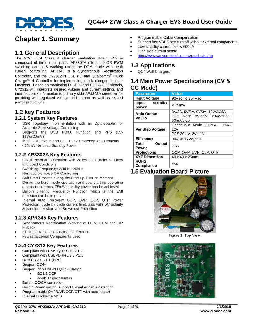
1.5 Evaluation Board Picture ___________________ 2
Chapter 2. Power Supply Specification __________ 3
2.1 Specification and Test Results _______________ 3
2.2 Compliance ______________________________ 3
3.1 EV3 Board Schematic ______________________ 4
3.2 Bill of Material (BOM) ______________________ 5 3.2.1 Power Main Board __________________________ 5 3.2.1 Controller Daughter Board (EV3) _______________ 5
3.3 Schematics Description _____________________ 6 3.3.1 AC Input Circuit & Differential Filter ____________ 6 3.3.2 AP3302A PWM Controller ____________________ 6 3.3.3 APR345 Synchronous Rectification (SR) MOSFET Driver _________________________________________ 6 3.3.4 CY2312 QC4/4+ Decoder & Protection on/off P MOSFET and Interface to Power Devices _____________ 6
Chapter 4. The Evaluation Board (EVB) Connections 7
4.1 EVB PCB Layout ___________________________ 7
4.2 Quick Start Guide Before Connection _________ 7
4.3 System Setup _____________________________ 9 4.3.1 Connection with E-Load ______________________ 9 4.3.2 USBCEE Power Adapter Tester (PAT) ____________ 9 4.3.3 Input & Output Wires Connection _____________ 10
Chapter 5. Testing the Evaluation Board _______ 11
5.1 Input & Output Characteristics ______________ 11 5.1.1 Input Standby Power _______________________ 11 5.1.2 Input Power Efficiency at Different AC Line Input Voltage _______________________________________ 11 5.1.3 Average Efficiency at Different Loading _________ 12
5.2 Output CV & CC Mode Testing ______________ 13 5.2.1 PPS Mode I-V Curve ________________________ 13 5.2.2 Fixed Mode I-V Curve ______________________ 14
5.3 QC Series Compatible Mode Testing __________ 15 5.3.1 QC 2.0 Mode Testing ______________________ 15 5.3.2 QC 3.0 Continuous Mode 200mV/Step Testing __ 15 5.3.3 QC4/4+ CV Accuracy 20mV/Step Testing (PPS Support) _____________________________________ 17 5.3.4 QC4/4+ CC Accuracy 50mA/Step Testing (PPS Support) _____________________________________ 18
5.4 Key Performance Waveforms _______________ 19 5.4.1 AC Input Requirements _____________________ 19 5.4.2 AC Line Slow Transients (Sag/Surge) __________ 20 5.4.3 27W QC4/4+ System Start-up Time & Hold-up Time _____________________________________________ 21 5.4.4 Q1 /Q2 Main Switching Voltage MOSFET Stress on at 12V/ 2.25A Loading ____________________________ 21 5.4.5 System Output Ripple & Noise with @ 1.2m Cable End _________________________________________ 22 5.4.6 Output Voltage Transition Time ______________ 23 5.4.7 Thermal Testing ___________________________ 24 5.4.8 EMI (CE) Testing ___________________________ 25
QC4/4+ 27W Class A Charger EV3 Board User Guide
QC4/4+ 27W AP3302A+APR345+CY2312 Page 2 of 26 2/1/2018 Release 1.0 www.diodes.com
Chapter 1. Summary 1.1 General Description The 27W QC4 Class A charger Evaluation Board EV3 is composed of three main parts, AP3302A offers the QR PWM switching control & working under the DCM mode with peak current controlling, APR345 is a Synchronous Rectification
Controller, and the CY2312 is USB PD and Qualcomm
Quick
Charge 4 Controller for implementing quick charger decoder functions. Based on monitoring D+ & D- and CC1 & CC2 signals, CY2312 will interprets desired voltage and current setting, and then feedback information to primary side AP3302A controller for providing well-regulated voltage and current as well as related power protections.
1.2 key Features 1.2.1 System Key Features SSR Topology Implementation with an Opto-coupler for
Accurate Step Voltage Controlling
Supports the USB PD3.0 Function and PPS (3V-11V@20mV)
Meet DOE level 6 and CoC Tier 2 Efficiency Requirements
<75mW No-Load Standby Power
1.2.2 AP3302A Key Features Quasi-Resonant Operation with Valley Lock under all Lines
and Load Conditions
Switching Frequency: 22kHz-120kHz
Non-audible-noise QR Controlling
Soft Start Process during the Start-up Turn-on Moment
During the burst mode operation and Low start-up operating quiescent currents, 75mW standby power can be achieved
Built-in Jittering Frequency Function which is the EMI emission can be improved
Internal Auto Recovery OCP, OVP, OLP, OTP Power Protection, cycle by cycle current limit, also with DC polarity & transformer short and Brown out Protection
1.2.3 APR345 Key Features Synchronous Rectification Working at DCM, CCM and QR
Flyback
Eliminate Resonant Ringing Interference
Fewest External Components used
1.2.4 CY2312 Key Features Compliant with USB Type-C Rev 1.2
Compliant with USBPD Rev.3.0 V1.1
USB PD 3.0 v1.1 (PPS)
Support QC4+
Support non-USBPD Quick Charge
BC1.2 DCP
Apple Legacy built-in
Built in CC/CV controller
Built in Vconn switch, support E-marker cable detection
Programmable OVP/UVP/OCP/OTP with auto-restart
Internal Discharge MOS
Programmable Cable Compensation
Support fast VBUS fast turn off without external components
Low standby current below 600uA
High side current sense
http://www.canyon-semi.com.tw/products.php
1.3 Applications QC4 Wall Chargers
1.4 Main Power Specifications (CV & CC Mode)
Parameter Value Input Voltage 90Vac to 264Vac
Input standby power
< 75mW
Main Output Vo / Io
3V/3A, 5V/3A, 9V/3A, 12V/2.25A
PPS Mode 3V-11V, 20mV/step, 50mA/step
Per Step Voltage Continuous Mode 200mV, 3.6V-12V
PPS 20mV, 3V-11V
Efficiency 88% at 12V/2.25A
Total Output Power
27W
Protections OCP, OVP, UVP, OLP, OTP
XYZ Dimension 40 x 40 x 25mm
ROHS Compliance
Yes
1.5 Evaluation Board Picture
Figure 1: Top View
QC4/4+ 27W Class A Charger EV3 Board User Guide
QC4/4+ 27W AP3302A+APR345+CY2312 Page 3 of 26 2/1/2018 Release 1.0 www.diodes.com
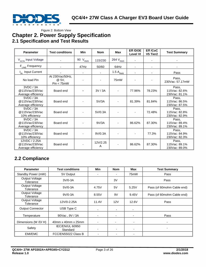
Figure 2: Bottom View
Chapter 2. Power Supply Specification 2.1 Specification and Test Results
Parameter Test conditions Min Nom Max Eff /DOE Level VI
Eff /CoC V5 Tier2
Test Summary
VACIN
Input Voltage - 90 VRMS
115/230 264 VRMS
- - -
FLINE
Frequency - 47Hz 50/60 64Hz - - -
IIN
Input Current - - - 1.5 ARMS
- - Pass
No load Pin At 230Vac/50Hz,
@ 5V, Pin < 75mW
- - 75mW - - Pass,
230Vac: 57.17mW
3VDC / 3A @115Vac/230Vac Average efficiency
Board end - 3V / 3A - 77.96% 78.23% Pass,
115Vac: 82.6% 230Vac: 81.1%
5VDC / 3A @115Vac/230Vac Average efficiency
Board end - 5V/3A - 81.39% 81.84% Pass,
115Vac: 86.5% 230Vac: 87.5%
5VDC / 3A @115Vac/230Vac
10% efficiency Board end - 5V/0.3A - - 72.48%
Pass, 115Vac: 82.8% 230Vac: 82.9%
9VDC / 3A @115Vac/230Vac Average efficiency
Board end - 9V/3A - 86.62% 87.30% Pass,
115Vac: 89.4% 230Vac: 89.1%
9VDC / 3A @115Vac/230Vac
10% efficiency Board end - 9V/0.3A - - 77.3%
Pass, 115Vac: 84.9% 230Vac: 82.3%
12VDC / 2.25A @115Vac/230Vac Average efficiency
Board end - 12V/2.25
A - 86.62% 87.30%
Pass, 115Vac: 89.1% 230Vac: 89.0%
2.2 Compliance
Parameter Test conditions Min Nom Max Test Summary
Standby Power (mW) 5V Output - - 75mW Pass
Output Voltage Tolerance
3V/0-3A 3V Pass
Output Voltage Tolerance
5V/0-3A 4.75V 5V 5.25V Pass (of 60mohm Cable end)
Output Voltage Tolerance
9V/0-3A 8.55V 9V 9.45V Pass (of 60mohm Cable end)
Output Voltage Tolerance
12V/0-2.25A 11.4V 12V 12.6V Pass
Output Connector USB Type C - - -
Temperature 90Vac , 9V / 3A - - - Pass
Dimensions (W /D/ H) 40mm x 40mm x 25mm - - - -
Safety IEC/EN/UL 60950
Standard - - - -
EMI/EMC FCC/EN55022 Class B - - -
QC4/4+ 27W Class A Charger EV3 Board User Guide
QC4/4+ 27W AP3302A+APR345+CY2312 Page 4 of 26 2/1/2018 Release 1.0 www.diodes.com
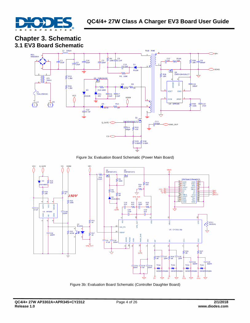
Chapter 3. Schematic 3.1 EV3 Board Schematic
Figure 3a: Evaluation Board Schematic (Power Main Board)
Figure 3b: Evaluation Board Schematic (Controller Daughter Board)
R39110K
C52.2nF
ZD115V
D1
RS1M
OP+
R2247K
R3810R
R3610R
C2227nF
R8
2R
Q_GATE
C4100pF
R131.8M
VDEM
R300.82R
R12
2R
C62.2uF
+C1022uF
D5
S07M
C310nF
R161.8M
F1T2AL/250VAC
R14A51R
VCC
+C8680uF+C2
15uF
R3 100K
GND_OUT
L1
L
1
L2 220uH
CS
R10 100K
T01B RM8
1
5
4
3
8
6
7
Q1
DMJ65H650SCTI
C124.7uF
C72.2uF
R4100K
Q3 DMN24H3D
CY1470pF
N1
N
1
Q2DMTH10H010LCT
+C115uF
SGNS
R290.82R
C132.2nF
+-~ ~
BD1MSB30KH
2
13
4C171nF
U4 APR345
1
23
4
5
6
AREF
GNDVDET
VC
C
CCM
DR
ISR
D3
1N4148
LF110mH
14
23
D2
S07M
C23100nF
R1551R
C2027nF
D+
D+R261K
C30100PF
Q4DMP2007UFG
GATE
D+
R330R
C94.7uF
R310R
R21N/A
D-
R25200K
150V
R340R
R2410K
C2710PF
R111K
R190.01R
C25560PF
VDEM
CN1Ty pe C ReceptacleA1A2A3A4A5A6A7A8A9
A10A11A12 B1
B2B3B4B5B6B7B8B9B10B11B12
GNDTX1+TX1-VOUTCC1D+D-SBU1VOUTRX2-RX2+GND GND
TX1+TX1-
VOUTCC2
D+D-
SBU1VOUTRX2-RX2+GND
CC1
VFB_OUT
R3249.9K
C21100nF
CC1
D61N4148WS
TVS1
DESD5V0S1BA
VFB_OUT
OP+
TVS3
DESD5V0S1BA
R171K
TVS2
DESD5V0S1BA
D4
1N4148WS
C29220PF
CS
C1568nF
U5 CY2311-16p14
1
2 3
4 5 6 7 8910
11
12
13
16
15
ISENP
V5V
IFB
VF
B
AG
ND
DP
DN
CC
1
CC
2
V18V
PG
ND
VB
US
PW
R_E
NB
VIN_PS VF
B_O
UT
OT
P
CC2
TVS4
DESD5V0S1BA
C18100nF
C2610PF
C24560PF
D-
U3 AP3302
1 2 3
6 5 4
GN
D
FB
DE
M
GA
TE
VC
C
SE
NS
E
CC2
C324.7uF
C114.7uF
R20R
VCC Q_GATE
GATE
t
NTC110K(N/A)
R2391K
Q5DMP2007UFG
U2EL1019
12
43
C16N/A
C31100nF
R1810R
C19N/A
R5100K
R9N/A
VBUS
R270R
R2010K
D-
QC4/4+ 27W Class A Charger EV3 Board User Guide
QC4/4+ 27W AP3302A+APR345+CY2312 Page 5 of 26 2/1/2018 Release 1.0 www.diodes.com
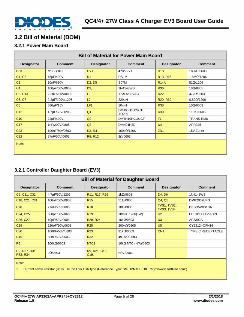
3.2 Bill of Material (BOM)
3.2.1 Power Main Board
Bill of Material for Power Main Board
Designator Comment Designator Comment Designator Comment
BD1 MSB30KH CY1 470pF/Y1 R10 100kΩ/0603
C1, C2 15µF/400V D1 RS1M R13, R16 1.8MΩ/1206
C3 10nF/630V D2, D5 S07M R14A 51Ω/1206
C4 100pF/50V/0603 D3, 1N4148WS R36 10Ω/0805
C5, C13 2.2nF/250V/0805 F1 T2AL/250VAC R22 47kΩ/0603
C6, C7 2.2µF/100V/1206 L2 220µH R29, R30 0.82Ω/1206
C8 680µF/16V LF1 10mH R38 10Ω/0603
C12 4.7µF/50V/1206 Q1 DMJ65H650SCTI, TO220
R39 110K//0603
C10 22µF/400V Q2 DMTH10H010LCT T1 TRANS-RM8
C17 1nF/200V/0805 Q3 DMN24H3D U4 APR345
C23 100nF/50v/0603 R3, R4 100kΩ/1206 ZD1 15V Zener
C22 27nF/50V/0603 R8, R12 2Ω/0603
Note:
3.2.1 Controller Daughter Board (EV3)
Bill of Material for Daughter Board
Designator Comment Designator Comment Designator Comment
C9, C11, C32 4.7µF/50V/1206 R11, R17, R26 1kΩ/0603 D4, D6 1N4148WS
C18, C21, C31 100nF/50V/0603 R15 51Ω/0805 Q4, Q5 DMP2007UFG
C20 27nF/50V/0603 R18 10Ω/0805 TVS1, TVS2,TVS3, TVS4
DESD5V0S1BA
C24, C25 560pF/50V/0603 R19 10mΩ 1206(1W) U2 EL1019 / LTV-1009
C26, C27 10pF/50V/0603 R20, R24 10kΩ/0603 U3 AP3302A
C29 220pF/50V/0603 R25 200kΩ/0805 U5 CY2312--QFN16
C30 100PF/50V/0603 R23 91kΩ/0603 CN1 TYPE C RECEPTACLE
C15 68nF/50V/0603 R32 49.9kΩ/0603
R5 100kΩ/0603 NTC1 10kΩ NTC (N/A)/0603
R2, R27, R31, R33, R34
0Ω/0603 R9, R21, C16, C19,
N/A /0603
Note:
1. Current sense resistor (R19) use the Low TCR type (Reference Type: SMF12M1FR010T “http://www.sartfuse.com”).
QC4/4+ 27W Class A Charger EV3 Board User Guide
QC4/4+ 27W AP3302A+APR345+CY2312 Page 6 of 26 2/1/2018 Release 1.0 www.diodes.com
3.3 Schematics Description
3.3.1 AC Input Circuit & Differential Filter There are three components in the section. The Fuse F1 protects against over-current conditions which occur when some main components failed. The LF1 is a common mode chock for the common mode noise suppression filleting because of the each coil with large impedance. The BD1 is rectifier, and basically converts alternating current & voltage into direct current & voltage. The C1, L2, C2, C3 & C10 are composted of the Pi filter for filtering the differential switching noise back to AC source.
3.3.2 AP3302A PWM Controller The AP3302A PWM controller U1 and Opto-Coupler U2 and Q1 are the power converting core components. Connected to filtered output after bridge circuit, R13 & R16 resistor path will provide start-up voltage and current during starting up through Vcc (Pin 5). Subsequent VCC power will be provided by voltage feedback from middle-tapped auxiliary winding through two options, R12-D5 and R8-D2-Q3-D3, depending on desired output voltage. This design is to accommodate with the required wide voltage range to support various protocols (including QC 4/USB PD Programmable Power Supply PPS), from 3V to 12V. Based on feedback of secondary side (Pin CATH of CY2312 Decoder) to primary side (FB pin of AP3302A) through Opto-coupler U2, AP3302A will switch ON and Off Q1 to regulate desired voltage and current on the secondary side.
3.3.3 APR345 Synchronous Rectification (SR) MOSFET Driver APR345 operates in DCM mode in this design and drives the Q2 MOSFET based on the secondary side transformer on/off ‘s duty cycle. As the power loss with the APR345-controlled MOSFET Q2 is less than that with Schottky Diodes, the total efficiency can be improved.
3.3.4 CY2312 QC4/4+ Decoder & Protection on/off P MOSFET and Interface to Power Devices The few sets of important pins provide critical protocol decoding and regulation functions in CY2312:
1) CC1 & CC2 (Pin 7, 8): CC1 & CC2 (Configuration Channel 1 & 2) are defined by USB PD spec to provide the channel
communication link between power source and sink devices.
2) D+ & D- (Pin 5, 6): While defined under USB PD for data transfer only, D+ and D- are used in QC4+ to provide voltage
information and backward compatibility with QC2.0 and QC3.0 devices.
3) Constant Voltage (CV): The CV is implemented by sensing VIN_PS (pin 13) via resistor divider and comparing with internal
reference voltage to generate a CV compensation signal on the VFB_OUT pin (pin 16). The output voltages can be adjusted
by firmware programming.
4) Constant Current (CC): The CC is implemented by sensing by current sense resistor (R19, 10mΩ) and current sense
amplifier, then comparing with internal programmable reference voltage to generate a compensation signal on VFB_OUT pin
(pin 16)
5) Loop Compensation: C15, R20 & C19 form the voltage loop compensation circuit, and C16, R21 & C20 form the current
loop compensation circuit.
6) VFB_OUT (Pin 16): It is the key interface link from secondary decoder (CY2312) to primary regulation circuit
(AP3302A). It is connected to Opto-coupler U2A cath for feedback information based all sensed CC1 & CC2, D+ & D- voltage
status for getting desired Vbus voltage & current.
7) PWR_ENB Driver (Pin 12) to PMOSFET Gate: The pin is used to turn on/off Vbus load switch (Q4 & Q5) to
enable/disable voltage output to the Vbus. An extra PMOSFET (Q5) is required to prevent reverse current from the attached
battery source.

QC4/4+ 27W Class A Charger EV3 Board User Guide
QC4/4+ 27W AP3302A+APR345+CY2312 Page 7 of 26 2/1/2018 Release 1.0 www.diodes.com
Chapter 4. The Evaluation Board (EVB) Connections
4.1 EVB PCB Layout
The thickness for both sides of PCB board trace cooper is 2 Oz.
Figure 4: PCB Board Layout Top View Figure 5: PCB Board Layout Bottom View
4.2 Quick Start Guide Before Connection
1) Before starting the QC4/4+ 27W EVB test, the end user needs to prepare the following tool,
software and manuals. For details, please contact Canyon Semiconductor local agent for further
information.
Test Kit: USBCEE Power Adapter Tester.
Software: USBCEE_Adavanced_Tester_Version 1.0.1 (file name: USBCEETester)
Firmware: CY2312PD20180119
To buy a USB-C POWER ADAPTER PROGRAMMER AND TESTER (white color) -
https://www.usbcee.com/
USBCEE PAT Tester USBCEE_Adavanced _Tester_V1.0.1 Standard-A to Micro-B Cable Type-C Cable
Figure 6: Canyon Items: Test Kit / PC Test GUI Software /Test Cables
QC4/4+ 27W Class A Charger EV3 Board User Guide
QC4/4+ 27W AP3302A+APR345+CY2312 Page 8 of 26 2/1/2018 Release 1.0 www.diodes.com
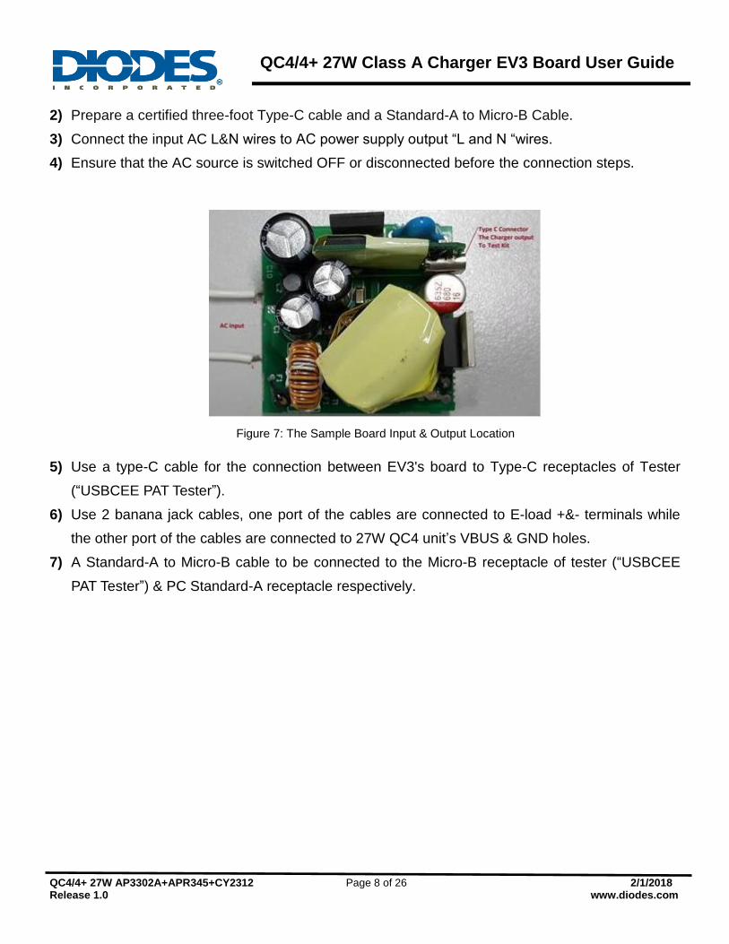
2) Prepare a certified three-foot Type-C cable and a Standard-A to Micro-B Cable.
3) Connect the input AC L&N wires to AC power supply output “L and N “wires.
4) Ensure that the AC source is switched OFF or disconnected before the connection steps.
Figure 7: The Sample Board Input & Output Location
5) Use a type-C cable for the connection between EV3's board to Type-C receptacles of Tester
(“USBCEE PAT Tester”).
6) Use 2 banana jack cables, one port of the cables are connected to E-load +&- terminals while
the other port of the cables are connected to 27W QC4 unit’s VBUS & GND holes.
7) A Standard-A to Micro-B cable to be connected to the Micro-B receptacle of tester (“USBCEE
PAT Tester”) & PC Standard-A receptacle respectively.
QC4/4+ 27W Class A Charger EV3 Board User Guide
QC4/4+ 27W AP3302A+APR345+CY2312 Page 9 of 26 2/1/2018 Release 1.0 www.diodes.com
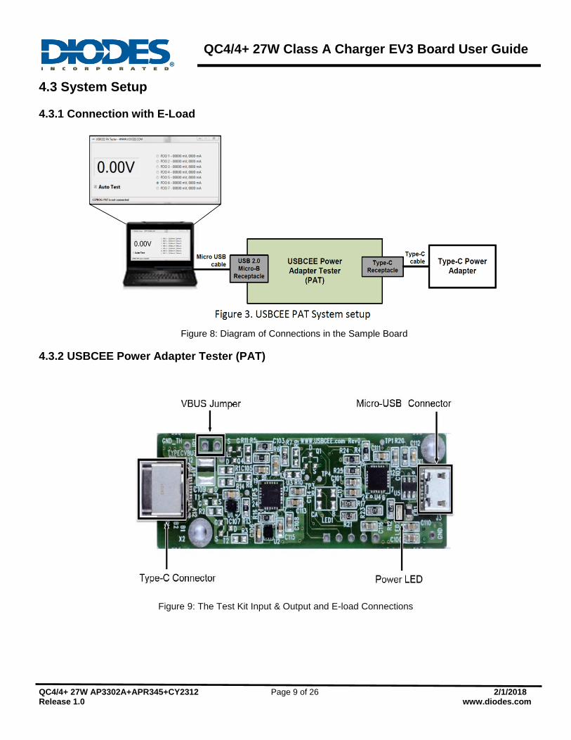
4.3 System Setup
4.3.1 Connection with E-Load
Figure 8: Diagram of Connections in the Sample Board
4.3.2 USBCEE Power Adapter Tester (PAT)
Figure 9: The Test Kit Input & Output and E-load Connections
QC4/4+ 27W Class A Charger EV3 Board User Guide
QC4/4+ 27W AP3302A+APR345+CY2312 Page 10 of 26 2/1/2018 Release 1.0 www.diodes.com
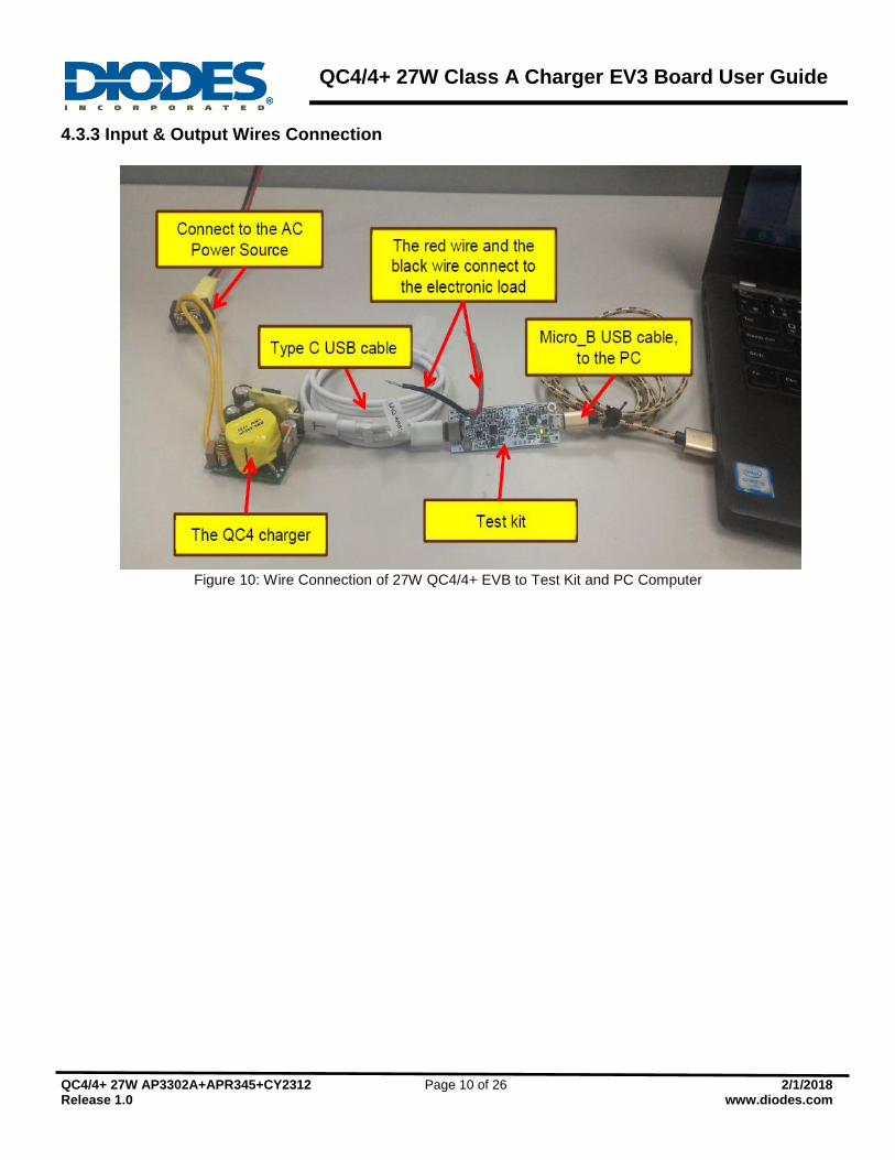
4.3.3 Input & Output Wires Connection
Figure 10: Wire Connection of 27W QC4/4+ EVB to Test Kit and PC Computer
QC4/4+ 27W Class A Charger EV3 Board User Guide
QC4/4+ 27W AP3302A+APR345+CY2312 Page 11 of 26 2/1/2018 Release 1.0 www.diodes.com
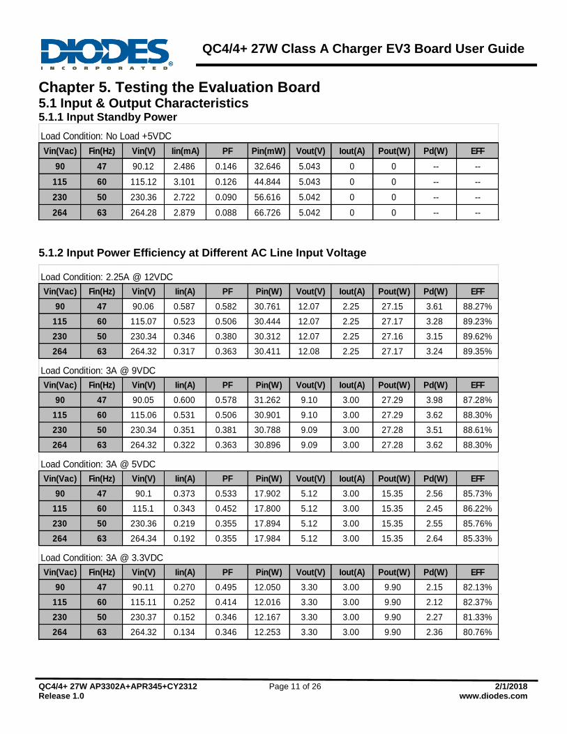
Chapter 5. Testing the Evaluation Board 5.1 Input & Output Characteristics 5.1.1 Input Standby Power
5.1.2 Input Power Efficiency at Different AC Line Input Voltage
Vin(Vac) Fin(Hz) Vin(V) Iin(mA) PF Pin(mW) Vout(V) Iout(A) Pout(W) Pd(W) EFF
90 47 90.12 2.486 0.146 32.646 5.043 0 0 -- --
115 60 115.12 3.101 0.126 44.844 5.043 0 0 -- --
230 50 230.36 2.722 0.090 56.616 5.042 0 0 -- --
264 63 264.28 2.879 0.088 66.726 5.042 0 0 -- --
Load Condition: No Load +5VDC
Vin(Vac) Fin(Hz) Vin(V) Iin(A) PF Pin(W) Vout(V) Iout(A) Pout(W) Pd(W) EFF
90 47 90.06 0.587 0.582 30.761 12.07 2.25 27.15 3.61 88.27%
115 60 115.07 0.523 0.506 30.444 12.07 2.25 27.17 3.28 89.23%
230 50 230.34 0.346 0.380 30.312 12.07 2.25 27.16 3.15 89.62%
264 63 264.32 0.317 0.363 30.411 12.08 2.25 27.17 3.24 89.35%
Vin(Vac) Fin(Hz) Vin(V) Iin(A) PF Pin(W) Vout(V) Iout(A) Pout(W) Pd(W) EFF
90 47 90.05 0.600 0.578 31.262 9.10 3.00 27.29 3.98 87.28%
115 60 115.06 0.531 0.506 30.901 9.10 3.00 27.29 3.62 88.30%
230 50 230.34 0.351 0.381 30.788 9.09 3.00 27.28 3.51 88.61%
264 63 264.32 0.322 0.363 30.896 9.09 3.00 27.28 3.62 88.30%
Vin(Vac) Fin(Hz) Vin(V) Iin(A) PF Pin(W) Vout(V) Iout(A) Pout(W) Pd(W) EFF
90 47 90.1 0.373 0.533 17.902 5.12 3.00 15.35 2.56 85.73%
115 60 115.1 0.343 0.452 17.800 5.12 3.00 15.35 2.45 86.22%
230 50 230.36 0.219 0.355 17.894 5.12 3.00 15.35 2.55 85.76%
264 63 264.34 0.192 0.355 17.984 5.12 3.00 15.35 2.64 85.33%
Vin(Vac) Fin(Hz) Vin(V) Iin(A) PF Pin(W) Vout(V) Iout(A) Pout(W) Pd(W) EFF
90 47 90.11 0.270 0.495 12.050 3.30 3.00 9.90 2.15 82.13%
115 60 115.11 0.252 0.414 12.016 3.30 3.00 9.90 2.12 82.37%
230 50 230.37 0.152 0.346 12.167 3.30 3.00 9.90 2.27 81.33%
264 63 264.32 0.134 0.346 12.253 3.30 3.00 9.90 2.36 80.76%
Load Condition: 2.25A @ 12VDC
Load Condition: 3A @ 9VDC
Load Condition: 3A @ 5VDC
Load Condition: 3A @ 3.3VDC
QC4/4+ 27W Class A Charger EV3 Board User Guide
QC4/4+ 27W AP3302A+APR345+CY2312 Page 12 of 26 2/1/2018 Release 1.0 www.diodes.com
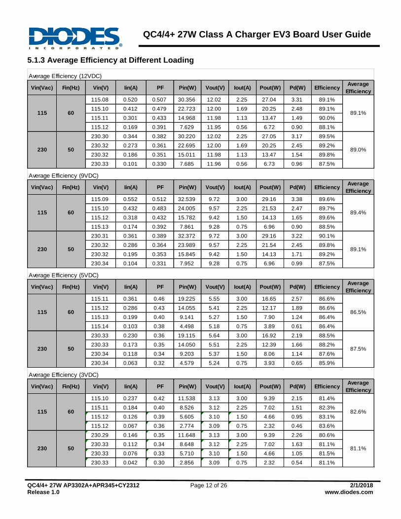
5.1.3 Average Efficiency at Different Loading
Vin(Vac) Fin(Hz) Vin(V) Iin(A) PF Pin(W) Vout(V) Iout(A) Pout(W) Pd(W) EfficiencyAverage
Efficiency
115.08 0.520 0.507 30.356 12.02 2.25 27.04 3.31 89.1%
115.10 0.412 0.479 22.723 12.00 1.69 20.25 2.48 89.1%
115.11 0.301 0.433 14.968 11.98 1.13 13.47 1.49 90.0%
115.12 0.169 0.391 7.629 11.95 0.56 6.72 0.90 88.1%
230.30 0.344 0.382 30.220 12.02 2.25 27.05 3.17 89.5%
230.32 0.273 0.361 22.695 12.00 1.69 20.25 2.45 89.2%
230.32 0.186 0.351 15.011 11.98 1.13 13.47 1.54 89.8%
230.33 0.101 0.330 7.685 11.96 0.56 6.73 0.96 87.5%
Vin(Vac) Fin(Hz) Vin(V) Iin(A) PF Pin(W) Vout(V) Iout(A) Pout(W) Pd(W) EfficiencyAverage
Efficiency
115.09 0.552 0.512 32.539 9.72 3.00 29.16 3.38 89.6%
115.10 0.432 0.483 24.005 9.57 2.25 21.53 2.47 89.7%
115.12 0.318 0.432 15.782 9.42 1.50 14.13 1.65 89.6%
115.13 0.174 0.392 7.861 9.28 0.75 6.96 0.90 88.5%
230.31 0.361 0.389 32.372 9.72 3.00 29.16 3.22 90.1%
230.32 0.286 0.364 23.989 9.57 2.25 21.54 2.45 89.8%
230.32 0.195 0.353 15.845 9.42 1.50 14.13 1.71 89.2%
230.34 0.104 0.331 7.952 9.28 0.75 6.96 0.99 87.5%
Vin(Vac) Fin(Hz) Vin(V) Iin(A) PF Pin(W) Vout(V) Iout(A) Pout(W) Pd(W) EfficiencyAverage
Efficiency
115.11 0.361 0.46 19.225 5.55 3.00 16.65 2.57 86.6%
115.12 0.286 0.43 14.055 5.41 2.25 12.17 1.89 86.6%
115.13 0.199 0.40 9.141 5.27 1.50 7.90 1.24 86.4%
115.14 0.103 0.38 4.498 5.18 0.75 3.89 0.61 86.4%
230.33 0.230 0.36 19.115 5.64 3.00 16.92 2.19 88.5%
230.33 0.173 0.35 14.050 5.51 2.25 12.39 1.66 88.2%
230.34 0.118 0.34 9.203 5.37 1.50 8.06 1.14 87.6%
230.34 0.063 0.32 4.579 5.24 0.75 3.93 0.65 85.9%
Vin(Vac) Fin(Hz) Vin(V) Iin(A) PF Pin(W) Vout(V) Iout(A) Pout(W) Pd(W) EfficiencyAverage
Efficiency
115.10 0.237 0.42 11.538 3.13 3.00 9.39 2.15 81.4%
115.11 0.184 0.40 8.526 3.12 2.25 7.02 1.51 82.3%
115.12 0.126 0.39 5.605 3.10 1.50 4.66 0.95 83.1%
115.12 0.067 0.36 2.774 3.09 0.75 2.32 0.46 83.6%
230.29 0.146 0.35 11.648 3.13 3.00 9.39 2.26 80.6%
230.33 0.112 0.34 8.648 3.12 2.25 7.02 1.63 81.1%
230.33 0.076 0.33 5.710 3.10 1.50 4.66 1.05 81.5%
230.33 0.042 0.30 2.856 3.09 0.75 2.32 0.54 81.1%
89.1%
89.0%
230 50 81.1%
Average Efficiency (3VDC)
115 60 86.5%
230 50 87.5%
Average Efficiency (9VDC)
Average Efficiency (12VDC)
Average Efficiency (5VDC)
115 60 82.6%
115 60 89.4%
230 50 89.1%
115
230
60
50
QC4/4+ 27W Class A Charger EV3 Board User Guide
QC4/4+ 27W AP3302A+APR345+CY2312 Page 13 of 26 2/1/2018 Release 1.0 www.diodes.com
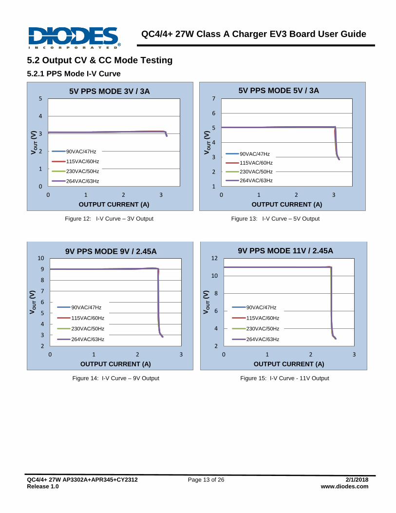
5.2 Output CV & CC Mode Testing
5.2.1 PPS Mode I-V Curve
Figure 12: I-V Curve – 3V Output Figure 13: I-V Curve – 5V Output
Figure 14: I-V Curve – 9V Output Figure 15: I-V Curve - 11V Output
0
1
2
3
4
5
0 1 2 3
VO
UT (
V)
OUTPUT CURRENT (A)
5V PPS MODE 3V / 3A
90VAC/47Hz
115VAC/60Hz
230VAC/50Hz
264VAC/63Hz 1
2
3
4
5
6
7
0 1 2 3
VO
UT (
V)
OUTPUT CURRENT (A)
5V PPS MODE 5V / 3A
90VAC/47Hz
115VAC/60Hz
230VAC/50Hz
264VAC/63Hz
2
3
4
5
6
7
8
9
10
0 1 2 3
VO
UT (
V)
OUTPUT CURRENT (A)
9V PPS MODE 9V / 2.45A
90VAC/47Hz
115VAC/60Hz
230VAC/50Hz
264VAC/63Hz
2
4
6
8
10
12
0 1 2 3
VO
UT (
V)
OUTPUT CURRENT (A)
9V PPS MODE 11V / 2.45A
90VAC/47Hz
115VAC/60Hz
230VAC/50Hz
264VAC/63Hz
QC4/4+ 27W Class A Charger EV3 Board User Guide
QC4/4+ 27W AP3302A+APR345+CY2312 Page 14 of 26 2/1/2018 Release 1.0 www.diodes.com
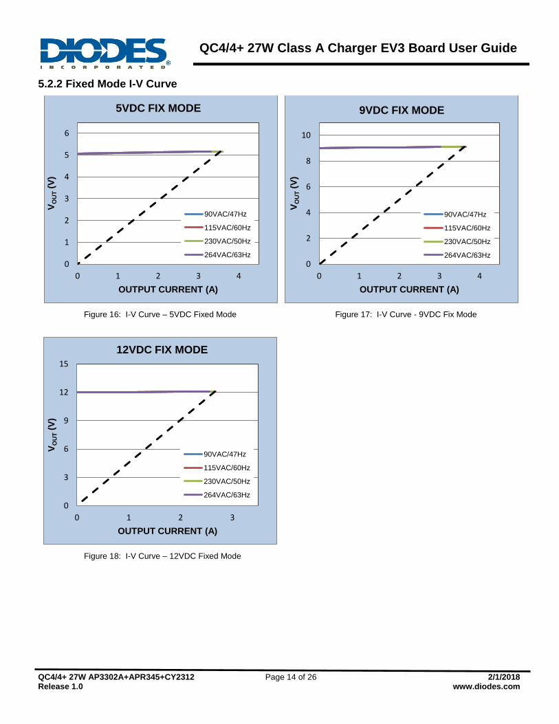
5.2.2 Fixed Mode I-V Curve
Figure 16: I-V Curve – 5VDC Fixed Mode Figure 17: I-V Curve - 9VDC Fix Mode
Figure 18: I-V Curve – 12VDC Fixed Mode
0
1
2
3
4
5
6
0 1 2 3 4
VO
UT (
V)
OUTPUT CURRENT (A)
5VDC FIX MODE
90VAC/47Hz
115VAC/60Hz
230VAC/50Hz
264VAC/63Hz
0
2
4
6
8
10
0 1 2 3 4
VO
UT (
V)
OUTPUT CURRENT (A)
9VDC FIX MODE
90VAC/47Hz
115VAC/60Hz
230VAC/50Hz
264VAC/63Hz
0
3
6
9
12
15
0 1 2 3
VO
UT (
V)
OUTPUT CURRENT (A)
12VDC FIX MODE
90VAC/47Hz
115VAC/60Hz
230VAC/50Hz
264VAC/63Hz
QC4/4+ 27W Class A Charger EV3 Board User Guide
QC4/4+ 27W AP3302A+APR345+CY2312 Page 15 of 26 2/1/2018 Release 1.0 www.diodes.com
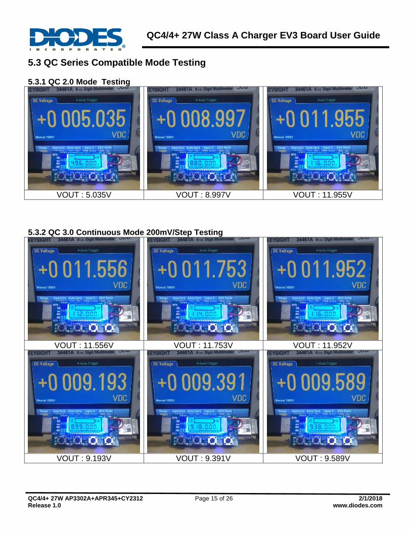
5.3 QC Series Compatible Mode Testing 5.3.1 QC 2.0 Mode Testing
VOUT : 5.035V VOUT : 8.997V VOUT : 11.955V
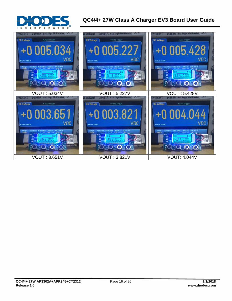
5.3.2 QC 3.0 Continuous Mode 200mV/Step Testing
VOUT : 11.556V VOUT : 11.753V VOUT : 11.952V
VOUT : 9.193V VOUT : 9.391V VOUT : 9.589V
QC4/4+ 27W Class A Charger EV3 Board User Guide
QC4/4+ 27W AP3302A+APR345+CY2312 Page 16 of 26 2/1/2018 Release 1.0 www.diodes.com
VOUT : 5.034V VOUT : 5.227V VOUT : 5.428V
VOUT : 3.651V VOUT : 3.821V VOUT: 4.044V
QC4/4+ 27W Class A Charger EV3 Board User Guide
QC4/4+ 27W AP3302A+APR345+CY2312 Page 17 of 26 2/1/2018 Release 1.0 www.diodes.com
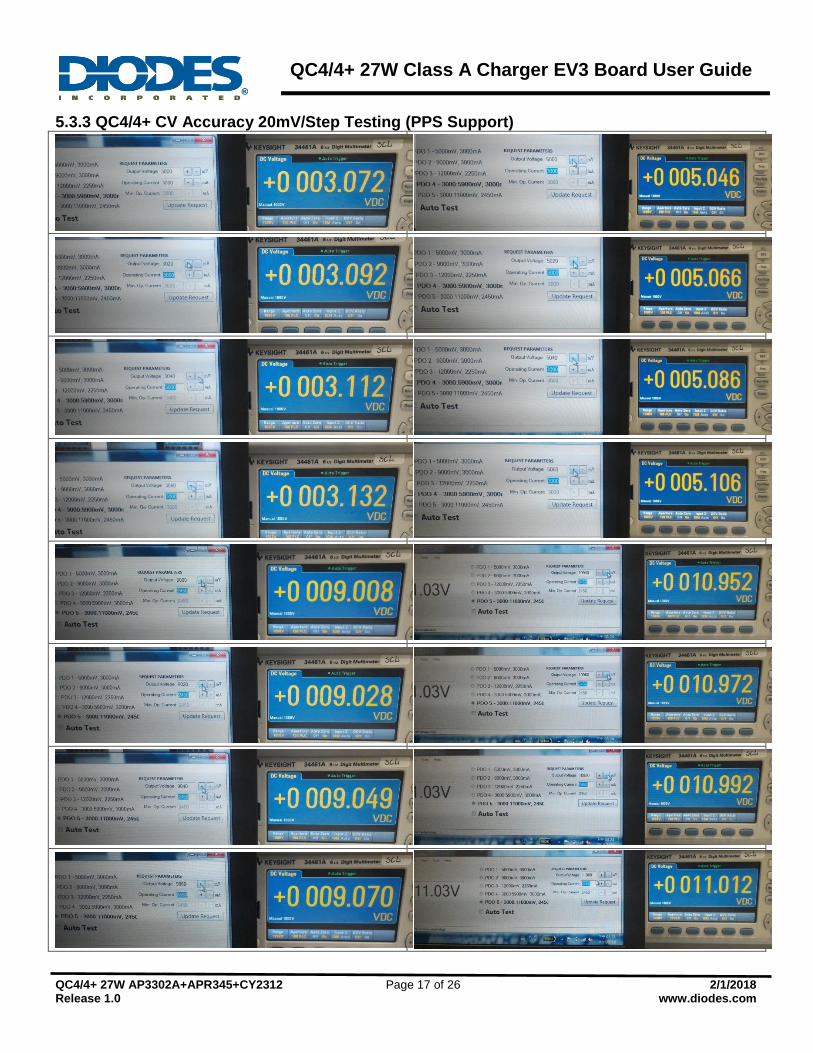
5.3.3 QC4/4+ CV Accuracy 20mV/Step Testing (PPS Support)
QC4/4+ 27W Class A Charger EV3 Board User Guide
QC4/4+ 27W AP3302A+APR345+CY2312 Page 18 of 26 2/1/2018 Release 1.0 www.diodes.com
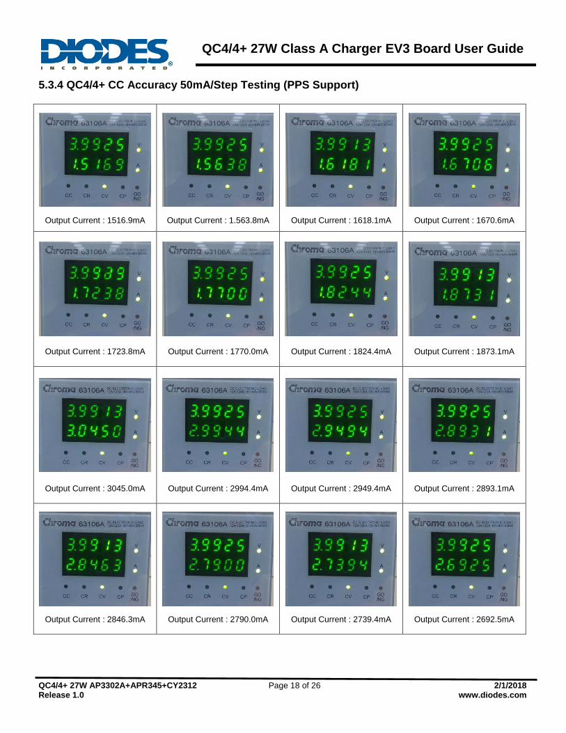
5.3.4 QC4/4+ CC Accuracy 50mA/Step Testing (PPS Support)
Output Current : 1516.9mA Output Current : 1.563.8mA Output Current : 1618.1mA Output Current : 1670.6mA
Output Current : 1723.8mA Output Current : 1770.0mA Output Current : 1824.4mA Output Current : 1873.1mA
Output Current : 3045.0mA Output Current : 2994.4mA Output Current : 2949.4mA Output Current : 2893.1mA
Output Current : 2846.3mA Output Current : 2790.0mA Output Current : 2739.4mA Output Current : 2692.5mA

QC4/4+ 27W Class A Charger EV3 Board User Guide
QC4/4+ 27W AP3302A+APR345+CY2312 Page 19 of 26 2/1/2018 Release 1.0 www.diodes.com
5.4 Key Performance Waveforms 5.4.1 AC Input Requirements AC Brownout on/off
Input AC Reading
Turn_Off Max Load 73.54Vac
Min Load 72.38Vac
Turn_On Max Load 80.43Vac
Min Load 81.48Vac
Figure 19 Figure 20
Figure 21 Figure 22
QC4/4+ 27W Class A Charger EV3 Board User Guide
QC4/4+ 27W AP3302A+APR345+CY2312 Page 20 of 26 2/1/2018 Release 1.0 www.diodes.com
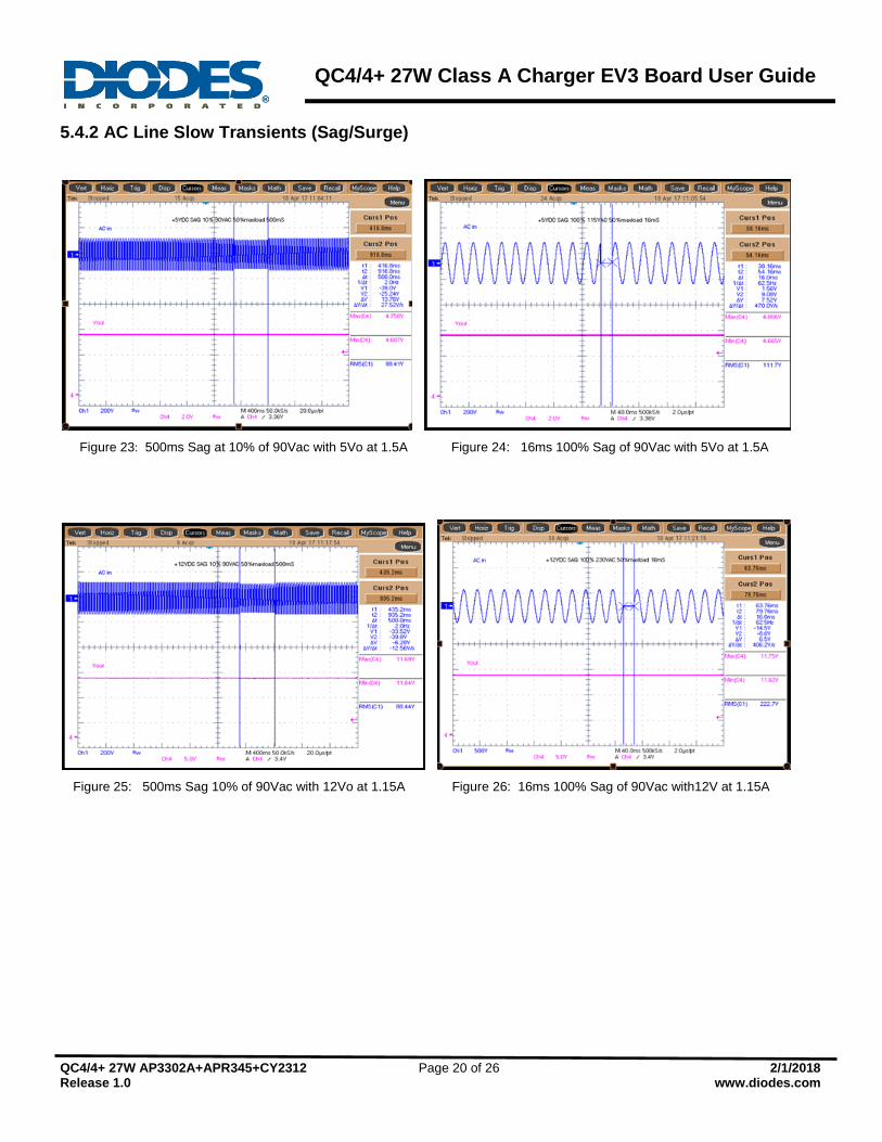
5.4.2 AC Line Slow Transients (Sag/Surge)
Figure 23: 500ms Sag at 10% of 90Vac with 5Vo at 1.5A Figure 24: 16ms 100% Sag of 90Vac with 5Vo at 1.5A
Figure 25: 500ms Sag 10% of 90Vac with 12Vo at 1.15A Figure 26: 16ms 100% Sag of 90Vac with12V at 1.15A
QC4/4+ 27W Class A Charger EV3 Board User Guide
QC4/4+ 27W AP3302A+APR345+CY2312 Page 21 of 26 2/1/2018 Release 1.0 www.diodes.com
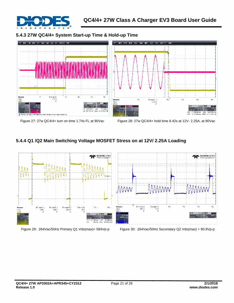
5.4.3 27W QC4/4+ System Start-up Time & Hold-up Time
Figure 27: 27w QC4/4+ turn on time 1.74s FL at 90Vac Figure 28: 27w QC4/4+ hold time 8.42s at 12V- 2.25A, at 90Vac
5.4.4 Q1 /Q2 Main Switching Voltage MOSFET Stress on at 12V/ 2.25A Loading
Figure 29: 264Vac/50Hz Primary Q1 Vds(max)= 584Vp-p Figure 30: 264Vac/50Hz Secondary Q2 Vds(max) = 90.9Vp-p
QC4/4+ 27W Class A Charger EV3 Board User Guide
QC4/4+ 27W AP3302A+APR345+CY2312 Page 22 of 26 2/1/2018 Release 1.0 www.diodes.com
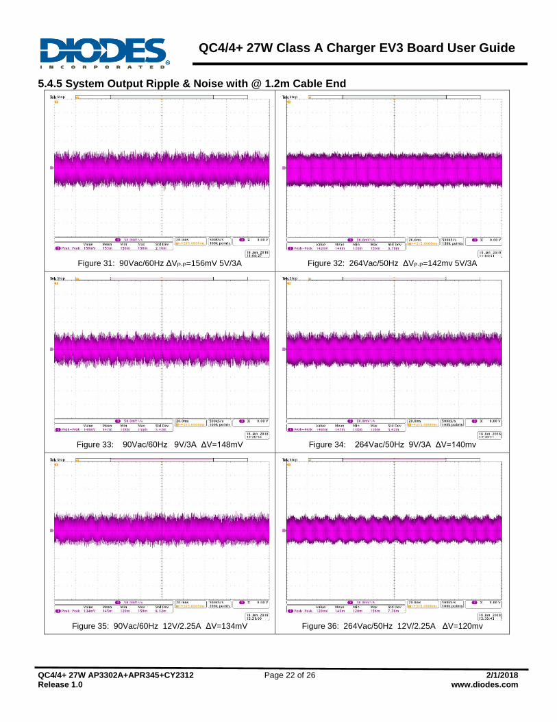
5.4.5 System Output Ripple & Noise with @ 1.2m Cable End
Figure 31: 90Vac/60Hz ΔVP-P=156mV 5V/3A Figure 32: 264Vac/50Hz ΔVP-P=142mv 5V/3A
Figure 33: 90Vac/60Hz 9V/3A ΔV=148mV Figure 34: 264Vac/50Hz 9V/3A ΔV=140mv
Figure 35: 90Vac/60Hz 12V/2.25A ΔV=134mV Figure 36: 264Vac/50Hz 12V/2.25A ΔV=120mv

QC4/4+ 27W Class A Charger EV3 Board User Guide
QC4/4+ 27W AP3302A+APR345+CY2312 Page 23 of 26 2/1/2018 Release 1.0 www.diodes.com
5.4.6 Output Voltage Transition Time
Figure 37: 5V→9V Rise Time: 43.06ms Figure 38: 9V→12V Rise Time: 31.8ms
Figure 39: 12V→9V Fall Time: 32.88ms Figure 40: 9V→5V Fall Time: 43.53ms
Figure 41: 5V→12V Fall Time: 75.33ms Figure 42: 12V→5V Fall Time: 76.33ms
QC4/4+ 27W Class A Charger EV3 Board User Guide
QC4/4+ 27W AP3302A+APR345+CY2312 Page 24 of 26 2/1/2018 Release 1.0 www.diodes.com
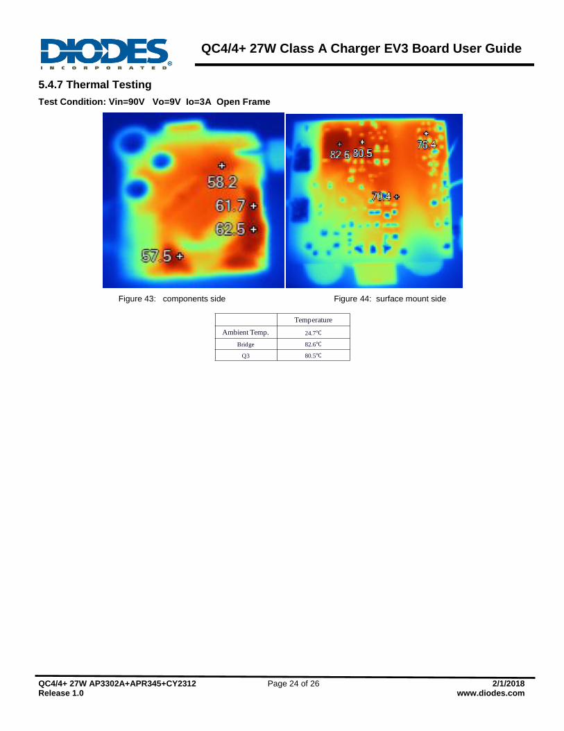
5.4.7 Thermal Testing
Test Condition: Vin=90V Vo=9V Io=3A Open Frame
Figure 43: components side Figure 44: surface mount side
Temperature
Ambient Temp. 24.7
Bridge 82.6
Q3 80.5
QC4/4+ 27W Class A Charger EV3 Board User Guide
QC4/4+ 27W AP3302A+APR345+CY2312 Page 25 of 26 2/1/2018 Release 1.0 www.diodes.com
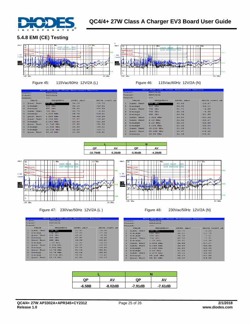
5.4.8 EMI (CE) Testing
Figure 45: 115Vac/60Hz 12V/2A (L) Figure 46: 115Vac/60Hz 12V/2A (N)
Figure 47: 230Vac/50Hz 12V/2A (L ) Figure 48: 230Vac/50Hz 12V/2A (N)
L N
QP AV QP AV
-10.79dB -5.26dB -5.95dB -4.28dB
L N
QP AV QP AV
-6.58B -8.02dB -7.91dB -7.61dB
QC4/4+ 27W Class A Charger EV3 Board User Guide
QC4/4+ 27W AP3302A+APR345+CY2312 Page 26 of 26 2/1/2018 Release 1.0 www.diodes.com
IMPORTANT NOTICE DIODES INCORPORATED MAKES NO WARRANTY OF ANY KIND, EXPRESS OR IMPLIED, WITH REGARDS TO THIS DOCUMENT, INCLUDING, BUT NOT LIMITED TO, THE IMPLIED WARRANTIES OF MERCHANTABILITY AND FITNESS FOR A PARTICULAR PURPOSE (AND THEIR EQUIVALENTS UNDER THE LAWS OF ANY JURISDICTION). Diodes Incorporated and its subsidiaries reserve the right to make modifications, enhancements, improvements, corrections or other changes without further notice to this document and any product described herein. Diodes Incorporated does not assume any liability arising out of the application or use of this document or any product described herein; neither does Diodes Incorporated convey any license under its patent or trademark rights, nor the rights of others. Any Customer or user of this document or products described herein in such applications shall assume all risks of such use and will agree to hold Diodes Incorporated and all the companies whose products are represented on Diodes Incorporated website, harmless against all damages. Diodes Incorporated does not warrant or accept any liability whatsoever in respect of any products purchased through unauthorized sales channel. Should Customers purchase or use Diodes Incorporated products for any unintended or unauthorized application, Customers shall indemnify and hold Diodes Incorporated and its representatives harmless against all claims, damages, expenses, and attorney fees arising out of, directly or indirectly, any claim of personal injury or death associated with such unintended or unauthorized application. Products described herein may be covered by one or more United States, international or foreign patents pending. Product names and markings noted herein may also be covered by one or more United States, international or foreign trademarks. This document is written in English but may be translated into multiple languages for reference. Only the English version of this document is the final and determinative format released by Diodes Incorporated.
LIFE SUPPORT Diodes Incorporated products are specifically not authorized for use as critical components in life support devices or systems without the express written approval of the Chief Executive Officer of Diodes Incorporated. As used herein: A. Life support devices or systems are devices or systems which: 1. are intended to implant into the body, or
2. support or sustain life and whose failure to perform when properly used in accordance with instructions for use provided in the labeling can be reasonably expected to result in significant injury to the user.
B. A critical component is any component in a life support device or system whose failure to perform can be reasonably expected to cause the failure of the life support device or to affect its safety or effectiveness. Customers represent that they have all necessary expertise in the safety and regulatory ramifications of their life support devices or systems, and acknowledge and agree that they are solely responsible for all legal, regulatory and safety-related requirements concerning their products and any use of Diodes Incorporated products in such safety-critical, life support devices or systems, notwithstanding any devices- or systems-related information or support that may be provided by Diodes Incorporated. Further, Customers must fully indemnify Diodes Incorporated and its representatives against any damages arising out of the use of Diodes Incorporated products in such safety-critical, life support devices or systems. Copyright © 2017, Diodes Incorporated www.diodes.com