qi compliant wireless power transmitter - texas instruments
TRANSCRIPT
AC-DCVoltage
Conditioning
Controller
RectificationPower
StageLoad
bq500210
Power
Transmitter Receiver
bq51013
Communication
bq500210
www.ti.com SLUSAL8C –JUNE 2011–REVISED SEPTEMBER 2012
Qi Compliant Wireless Power Transmitter ManagerCheck for Samples: bq500210
1FEATURES APPLICATIONS• Intelligent Control of the Power Transfer • WPC 1.0.2 Compliant Wireless Chargers for:
between Base Station and Mobile Device – Mobile and Smart Phones• Conforms to the Wireless Power Consortium – MP3 Players
(WPC) Wireless Power Transfer 1.0.2 – Global Positioning DevicesSpecification
– Digital Cameras• Digital Demodulation Significantly Simplifies
• Other Wireless Power Transmitters in:Solution Over bq500110– Cars and Other Vehicles• Improved Parasitic Metal Object Detection– Hermetically Sealed Devices, Tools, and(PMOD) Promotes Safety During Wireless
AppliancesPower Transfer– Furniture Built-In Wireless Chargers• Enhanced Charge Status Indicator– Toy Power Supplies and Chargers• Operating Modes Status Indicators
• See www.ti.com/wirelesspower for More– StandbyInformation on TI's Wireless Charging– Power Transfer (visual and audio)Solutions
– Charge Complete– Fault
• Over Temperature Protection
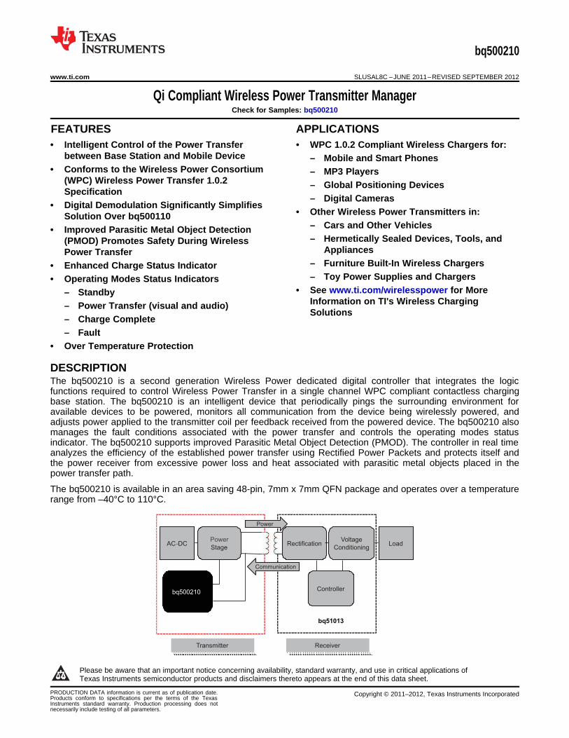
DESCRIPTIONThe bq500210 is a second generation Wireless Power dedicated digital controller that integrates the logicfunctions required to control Wireless Power Transfer in a single channel WPC compliant contactless chargingbase station. The bq500210 is an intelligent device that periodically pings the surrounding environment foravailable devices to be powered, monitors all communication from the device being wirelessly powered, andadjusts power applied to the transmitter coil per feedback received from the powered device. The bq500210 alsomanages the fault conditions associated with the power transfer and controls the operating modes statusindicator. The bq500210 supports improved Parasitic Metal Object Detection (PMOD). The controller in real timeanalyzes the efficiency of the established power transfer using Rectified Power Packets and protects itself andthe power receiver from excessive power loss and heat associated with parasitic metal objects placed in thepower transfer path.
The bq500210 is available in an area saving 48-pin, 7mm x 7mm QFN package and operates over a temperaturerange from –40°C to 110°C.
1
Please be aware that an important notice concerning availability, standard warranty, and use in critical applications ofTexas Instruments semiconductor products and disclaimers thereto appears at the end of this data sheet.
PRODUCTION DATA information is current as of publication date. Copyright © 2011–2012, Texas Instruments IncorporatedProducts conform to specifications per the terms of the TexasInstruments standard warranty. Production processing does notnecessarily include testing of all parameters.

bq500210
SLUSAL8C –JUNE 2011–REVISED SEPTEMBER 2012 www.ti.com
These devices have limited built-in ESD protection. The leads should be shorted together or the device placed in conductive foamduring storage or handling to prevent electrostatic damage to the MOS gates.
ORDERING INFORMATION (1)
OPERATING TEMPERATURE TOP SIDEORDERABLE PART NUMBER PIN COUNT SUPPLY PACKAGERANGE, TA MARKING
bq500210RGZR 48 pin Reel of 2500 QFN bq500210-40°C to 110°C
bq500210RGZT 48 pin Reel of 250 QFN bq500210
(1) For the most current package and ordering information, see the Package Option Addendum at the end of this document, or see the TIweb site at www.ti.com.
ABSOLUTE MAXIMUM RATINGS (1)
over operating free-air temperature range (unless otherwise noted)
VALUEUNIT
MIN MAX
Voltage applied at V33D to DGND –0.3 3.8 V
Voltage applied at V33A to AGND –0.3 3.8 V
Voltage applied to any pin (2) –0.3 3.8 V
Storage temperature,TSTG –40 150 °C
(1) Stresses beyond those listed under absolute maximum ratings may cause permanent damage to the device. These are stress ratingsonly and functional operation of the device at these or any other conditions beyond those indicated under recommended operatingconditions is not implied. Exposure to absolute-maximum-rated conditions for extended periods may affect device reliability.
(2) All voltages referenced to GND.
THERMAL INFORMATIONbq500210
THERMAL METRIC (1) RGZ UNITS
48 PINS
θJA Junction-to-ambient thermal resistance (2) 28.4
θJC(top) Junction-to-case(top) thermal resistance (3) 13.9
θJB Junction-to-board thermal resistance (4) 5.3°C/W
ψJT Junction-to-top characterization parameter (5) 0.2
ψJB Junction-to-board characterization parameter (6) 5.2
θJC(bottom) Junction-to-case(bottom) thermal resistance (7) 1.4
(1) For more information about traditional and new thermal metrics, see the IC Package Thermal Metrics application report, SPRA953.(2) The junction-to-ambient thermal resistance under natural convection is obtained in a simulation on a JEDEC-standard, high-K board, as
specified in JESD51-7, in an environment described in JESD51-2a.(3) The junction-to-case (top) thermal resistance is obtained by simulating a cold plate test on the package top. No specific JEDEC-
standard test exists, but a close description can be found in the ANSI SEMI standard G30-88.(4) The junction-to-board thermal resistance is obtained by simulating in an environment with a ring cold plate fixture to control the PCB
temperature, as described in JESD51-8.(5) The junction-to-top characterization parameter, ψJT, estimates the junction temperature of a device in a real system and is extracted
from the simulation data for obtaining θJA, using a procedure described in JESD51-2a (sections 6 and 7).(6) The junction-to-board characterization parameter, ψJB, estimates the junction temperature of a device in a real system and is extracted
from the simulation data for obtaining θJA , using a procedure described in JESD51-2a (sections 6 and 7).(7) The junction-to-case (bottom) thermal resistance is obtained by simulating a cold plate test on the exposed (power) pad. No specific
JEDEC standard test exists, but a close description can be found in the ANSI SEMI standard G30-88.Spacer
2 Submit Documentation Feedback Copyright © 2011–2012, Texas Instruments Incorporated
Product Folder Links: bq500210

bq500210
www.ti.com SLUSAL8C –JUNE 2011–REVISED SEPTEMBER 2012
RECOMMENDED OPERATING CONDITIONSover operating free-air temperature range (unless otherwise noted)
MIN NOM MAX UNIT
V Supply voltage during operation, V33D, V33A 3.0 3.3 3.6 V
TA Operating free-air temperature range –40 125 °C
TJ Junction temperature 125 °C
ELECTRICAL CHARACTERISTICSover operating free-air temperature range (unless otherwise noted)
PARAMETER TEST CONDITIONS MIN NOM MAX UNIT
SUPPLY CURRENT
IV33A V33A = 3.3 V 8 15
IV33D V33D = 3.3 V 42 55Supply current mAV33D = 3.3 V while storing configurationIV33D 53 65parameters in flash memory
INTERNAL REGULATOR CONTROLLER INPUTS/OUTPUTS
V33 3.3-V linear regulator Emitter of NPN transistor 3.25 3.3 3.6V
V33FB 3.3-V linear regulator feedback 4 4.6
IV33FB Series pass base drive VIN = 12 V; current into V33FB pin 10 mA
Beta Series NPN pass device 40
EXTERNALLY SUPPLIED 3.3 V POWER
V33D Digital 3.3-V power TA = 25°C 3 3.6 V
V33A Analog 3.3-V power TA = 25°C 3 3.6 V
V33 slew rate between 2.3V and 2.9V,V33Slew V33 slew rate 0.25 V/msV33A = V33D
MODULATION AMPLIFIER INPUTS EAP-A, EAN-A, EAP-B, EAN-B
VCM Common mode voltage each pin –0.15 1.631 V
EAP-EAN Modulation voltage digital resolution 1 mV
REA Input Impedance Ground reference 0.5 1.5 3 MΩ
IOFFSET Input offset current 1 kΩ source impedance –5 5 µA
ANALOG INPUTS V_IN, I_IN, TEMP_IN, I_COIL, LED_MODE, PMOD_THR
VADDR_OPEN Voltage indicating open pin LED_MODE, PMOD_THR open 2.37 V
VADDR_SHORT Voltage indicating pin shorted to GND LED_MODE, PMOD_THR shorted to ground 0.36 V
VADC_RANGE Measurement range for voltage monitoring Inputs: V_IN, I_IN, TEMP_IN, I_COIL 0 2.5 V
INL ADC integral nonlinearity -2.5 2.5 mV
Ilkg Input leakage current 3V applied to pin 100 nA
RIN Input impedance Ground reference 8 MΩ
CIN Input capacitance 10 pF
DIGITAL INPUTS/OUTPUTS
DGND1VOL Low-level output voltage IOL = 6 mA (1), V33D = 3 V V+ 0.25
V33DVOH High-level output voltage IOH = -6 mA (2), V33D = 3 V V- 0.6V
VIH High-level input voltage V33D = 3V 2.1 3.6 V
VIL Low-level input voltage V33D = 3.5 V 1.4 V
IOH(MAX) Output high source current 4 mA
IOL(MAX) Output low sink current 4 mA
SYSTEM PERFORMANCE
VRESET Voltage where device comes out of reset V33D Pin 2.3 2.4 V
tRESET Pulse width needed for reset RESET pin 2 µs
FSW Switching Frequency 110 205 kHz
(1) The maximum IOL, for all outputs combined, should not exceed 12 mA to hold the maximum voltage drop specified.(2) The maximum IOH, for all outputs combined, should not exceed 48 mA to hold the maximum voltage drop specified.
Copyright © 2011–2012, Texas Instruments Incorporated Submit Documentation Feedback 3
Product Folder Links: bq500210
PWM
12-bit
ADC
mController
COMM_B+
COMM_B-
TEMP_INT
PWM-B (EN)
PMB_CLK
PMB_DATA
PWM-A
LED Control /
Low Power
Supervisor
Interface
I2C(PMBUS)
Debug/P
rogra
mm
ing
RESERVED
RESERVED
RESERVED
RESERVED
RESERVED
COMM_A+
COMM_A- Digital
Demodulation
TEMP_EXT
V_IN
I_OUT
Buzzer
Control BUZ_DC
BUZ_AC
Low Power
Control
SLEEP RESET
MSP430 CNTL
LED DRIVE
bq500210
bq500210
SLUSAL8C –JUNE 2011–REVISED SEPTEMBER 2012 www.ti.com
ELECTRICAL CHARACTERISTICS (continued)over operating free-air temperature range (unless otherwise noted)
PARAMETER TEST CONDITIONS MIN NOM MAX UNIT
Time to detect presence of device requestingtdetect 0.6 secpower
tretention Retention of configuration parameters TJ = 25°C 100 Years
Write_Cycles Number of nonvolatile erase/write cycles TJ = 25°C 20 K cycles
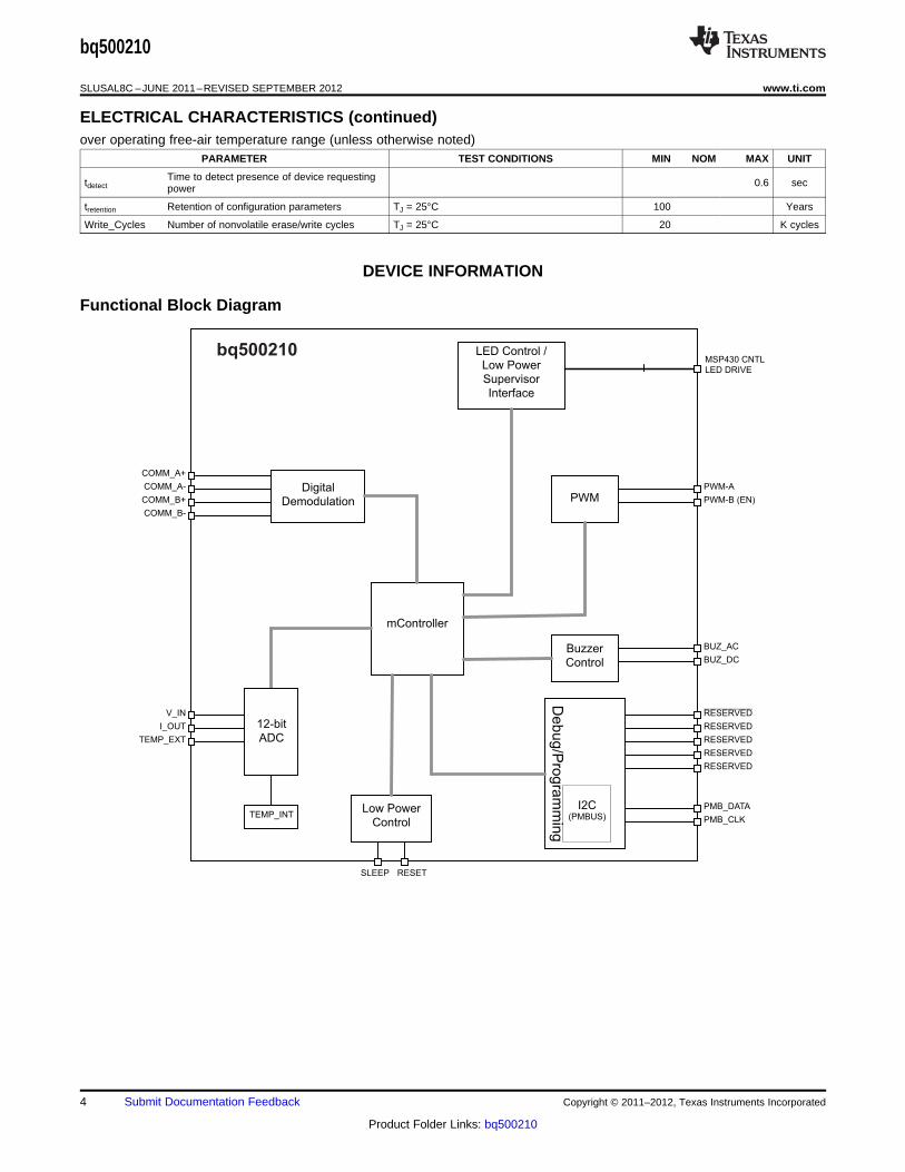
DEVICE INFORMATION
Functional Block Diagram
4 Submit Documentation Feedback Copyright © 2011–2012, Texas Instruments Incorporated
Product Folder Links: bq500210
V_IN
AIN
7
bq500210
48
47
46
45
44
43
42
41
40
39
33
32
31
30
29
28
27
26
25
13
14
15
18
19
21
16
17
3
4
5
6
7
8
9
10
11
12
34
22
20
RESET
AIN8
MSP_RST/LED_A
MSP_TEST
PMB _DATA
MSP_MISO/LED_B
PMB _CLK
DPWM _A
DP
MB
_B
MS
P_S
YN
C
DO
UT
_2
B
DO
UT
_4
A
PM
B_A
LR
T
PM
B_C
TR
L
MS
P_T
CK
/C
LK
RESERVED
RESERVED
RE
FIN
RESERVED
RESERVED
RESERVED
MSP_RDY
MSP_MOSI/LPWR_EN
DGND
AG
ND
LE
D_M
OD
E
AIN3
V3
3F
B
SLEEP
V33A
I_IN
V33D
23
24
BU
Z_A
C
BU
Z_D
C
38
37
1
2T_SENSE
AIN5
35
36 AGND
BPCAP
DO
UT
_4
B
DO
UT
_T
X
DR
V_C
FG
CO
MM
_A
+
CO
MM
_A
-
CO
MM
_B
+
CO
MM
_B
-
PM
OD
_T
HR
bq500210
www.ti.com SLUSAL8C –JUNE 2011–REVISED SEPTEMBER 2012
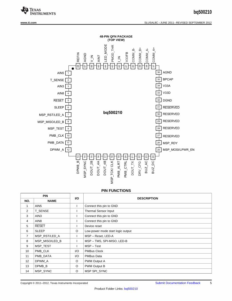
48-PIN QFN PACKAGE(TOP VIEW)
PIN FUNCTIONSPIN
I/O DESCRIPTIONNO. NAME
1 AIN5 I Connect this pin to GND
2 T_SENSE I Thermal Sensor Input
3 AIN3 I Connect this pin to GND
4 AIN8 I Connect this pin to GND
5 RESET I Device reset
6 SLEEP O Low-power mode start logic output
7 MSP_RST/LED_A I MSP – Reset, LED-A
8 MSP_MISO/LED_B I MSP – TMS, SPI-MISO, LED-B
9 MSP_TEST I MSP – Test
10 PMB_CLK I/O PMBus Clock
11 PMB_DATA I/O PMBus Data
12 DPWM_A O PWM Output A
13 DPMB_B O PWM Output B
14 MSP_SYNC O MSP SPI_SYNC
Copyright © 2011–2012, Texas Instruments Incorporated Submit Documentation Feedback 5
Product Folder Links: bq500210
bq500210
SLUSAL8C –JUNE 2011–REVISED SEPTEMBER 2012 www.ti.com
PIN FUNCTIONS (continued)
PINI/O DESCRIPTION
NO. NAME
15 DOUT_2B O Optional Logic Output 2B. Leave this pin floating.
16 DOUT_4A O Optional Logic Output 4A. Leave this pin floating.
17 DOUT_4B O Optional Logic Output 4B. Leave this pin floating.
18 MSP_TCK/CLK I/O Disable Diagnostic Output. Leave this pin floating to inhibit diagnostic.
19 PMB_ALERT O PMBus Interface
20 PMB_CTRL I PMBus Interface
21 DOUT_TX I Leave this pin floating
22 DRV_CFG I Pull this input to V33D
23 BUZ_AC O AC Buzzer Output
24 BUZ_DC O DC Buzzer Output
25 MSP_MOSI/LPWR_EN I/O MSP-TDI, SPI-MOSI, Low Power Enable
26 MSP_RDY I/O MSP-TDO, Programmed Indicator
27 RESERVED I/O Reserved, for factory use only
28 RESERVED I/O Reserved, for factory use only
29 RESERVED I/O Reserved, for factory use only
30 RESERVED I/O Reserved, for factory use only
31 RESERVED I/O Reserved, for factory use only
32 DGND — Digital GND
33 V33D — Digital Core 3.3V Supply
34 V33A — Analog 3.3V Supply
35 BPCAP — Bypass Capacitor Connect Pin
36 AGND — Analog GND
37 COMM_A+ I Digital demodulation noninverting input A
38 COMM_A- I Digital demodulation inverting input A
39 COMM_B+ I Digital demodulation noninverting input B
40 COMM_B- I Digital demodulation inverting input B
41 V33FB I 3.3V Linear-Regulator Feedback Input. Leave this pin floating.
42 I_IN I Transmitter Input Current
43 PMOD_THR I Input to Program Metal Object Detection Threshold
44 LED_MODE I Input to Select LED Mode
45 AIN7 I Reserved Analog Input. Connect this pin to GND.
46 V_IN I Transmitter Input Voltage
47 AGND — Analog GND
48 REFIN I External Reference Voltage Input. Connect this Input to AGND.
6 Submit Documentation Feedback Copyright © 2011–2012, Texas Instruments Incorporated
Product Folder Links: bq500210

0
0.2
0.4
0.6
0.8
1
1.2
1.4
0 1 2 3 4 5 6
P - Output Power - WO
R = 0 kPMOD W
R = 56.2 kPMOD W
R = 64.9 kPMOD W
R = 75 kPMOD W
Recti
fier
Lo
ad
ing
- W
R = 42.2 kPMOD W
R = 48.7 kPMOD W
50
55
60
65
70
75
80
100 300 500 700 900 1100
R - Load Current - mAL
Eff
icie
nc
y -
%
bq500210
www.ti.com SLUSAL8C –JUNE 2011–REVISED SEPTEMBER 2012
TYPICAL CHARACTERISTICS
SPACER
EFFICIENCY PMOD THRESHOLDvs vs
RECEIVER LOAD CURRENT OUTPUT POWER
Figure 1. Figure 2.
Copyright © 2011–2012, Texas Instruments Incorporated Submit Documentation Feedback 7
Product Folder Links: bq500210
Comm
Rectifier
Receiver Coil
ReceiverCapacitor
Modulation
Resitor
Amax
A(0)
A(1)
F, kHzFsw
Operating state at logic “0”
Operating state at logic “1”
a) b)
bq500210
SLUSAL8C –JUNE 2011–REVISED SEPTEMBER 2012 www.ti.com
FUNCTIONAL OVERVIEW
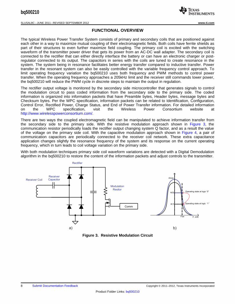
The typical Wireless Power Transfer System consists of primary and secondary coils that are positioned againsteach other in a way to maximize mutual coupling of their electromagnetic fields. Both coils have ferrite shields aspart of their structures to even further maximize field coupling. The primary coil is excited with the switchingwaveform of the transmitter power driver that gets its power from an AC-DC wall adapter. The secondary coil isconnected to the rectifier that can either directly interface the battery or can have an electronic charger or post-regulator connected to its output. The capacitors in series with the coils are tuned to create resonance in thesystem. The system being in resonance facilitates better energy transfer compared to inductive transfer. Powertransfer in the resonant system can also be easily controlled with the variable frequency control approach. Tolimit operating frequency variation the bq500210 uses both frequency and PWM methods to control powertransfer. When the operating frequency approaches a 205kHz limit and the receiver still commands lower power,the bq500210 will reduce the PWM cycle in discrete steps to maintain the output in regulation.
The rectifier output voltage is monitored by the secondary side microcontroller that generates signals to controlthe modulation circuit to pass coded information from the secondary side to the primary side. The codedinformation is organized into information packets that have Preamble bytes, Header bytes, message bytes andChecksum bytes. Per the WPC specification, information packets can be related to Identification, Configuration,Control Error, Rectified Power, Charge Status, and End of Power Transfer information. For detailed informationon the WPC specification, visit the Wireless Power Consortium website athttp://www.wirelesspowerconsortium.com/.
There are two ways the coupled electromagnetic field can be manipulated to achieve information transfer fromthe secondary side to the primary side. With the resistive modulation approach shown in Figure 3, thecommunication resistor periodically loads the rectifier output changing system Q factor, and as a result the valueof the voltage on the primary side coil. With the capacitive modulation approach shown in Figure 4, a pair ofcommunication capacitors are periodically connected to the receiver coil network. These extra capacitanceapplication changes slightly the resonance frequency of the system and its response on the current operatingfrequency, which in turn leads to coil voltage variation on the primary side.
With both modulation techniques primary side coil waveform variations are detected with a Digital Demodulationalgorithm in the bq500210 to restore the content of the information packets and adjust controls to the transmitter.
Figure 3. Resistive Modulation Circuit
8 Submit Documentation Feedback Copyright © 2011–2012, Texas Instruments Incorporated
Product Folder Links: bq500210

Comm
Rectifier
Receiver Coil
Receiver
Capacitor
Modulation
Capacitors
Amax
A(0)
A(1)
F, kHzFo(1) < Fo(0)
Operating state at logic “ 0”
Operating state at logic “ 1”
Fsw
a) b)
bq500210
www.ti.com SLUSAL8C –JUNE 2011–REVISED SEPTEMBER 2012
Figure 4. Capacitive Modulation Circuit
The bq500210 is a second generation wireless power dedicated transmitter controller that simplifies integration ofwireless power technology into consumer electronics, such as digital cameras, smart phones, MP3 players, andglobal positioning systems, along with infrastructure applications such as furniture and cars.
The bq500210 is a specialized digital power microcontroller that controls WPC A1, single coil, transmitterfunctions such as analog ping, digital ping, variable frequency output power control, parasitic metal objectdetection, over temperature protection of the transmitter top surface, and indication of the transmitter operatingstates.
The bq500210 digital demodulation inputs receive scaled down voltages from the transmitter resonantcomponents. The digital demodulation algorithm is a combination of several digital signal processing techniquesthat decodes information packets sent by the power receiving device and provides necessary changes to powerdrive signals facilitating closed loop regulation. The controller analog inputs monitor input DC voltage, inputcurrent, and the thermal protection input. These analog inputs support monitoring and protective functions of thecontroller.
The bq500210 controls two LEDs to indicate transmitter operating and fault states. Having the LEDs connecteddirectly to the controller simplifies the transmitter electrical schematic and provides a cost effective solution.
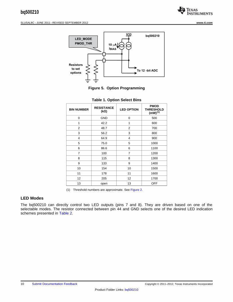
Option Select Pins
Two pins (43, 44) in the bq500210 are allocated to program the PMOD mode and the LED mode of the device.At power-up, a bias current is applied to pins LED_MODE and PMOD_THR and the resulting voltage measuredin order to identify the value of the attached programming resistor. The values of the operating parameters set bythese pins are determined using Option Select Bins. For LED_MODE, the selected bin determines the LEDbehavior based on LED Modes; for the PMOD_THR, the selected bin sets a threshold used for parasitic metalobject detection (see Metal Object Detection (PMOD) section).
Copyright © 2011–2012, Texas Instruments Incorporated Submit Documentation Feedback 9
Product Folder Links: bq500210
V33
10 Am
IBIAS
To 12 -bit ADC
Resistors
to set
options
LED_MODE
PMOD_THR
bq500210
bq500210
SLUSAL8C –JUNE 2011–REVISED SEPTEMBER 2012 www.ti.com
Figure 5. Option Programming
Table 1. Option Select Bins
PMODRESISTANCEBIN NUMBER LED OPTION THRESHOLD(kΩ) (mW) (1)
0 GND 0 500
1 42.2 1 600
2 48.7 2 700
3 56.2 3 800
4 64.9 4 900
5 75.0 5 1000
6 86.6 6 1100
7 100 7 1200
8 115 8 1300
9 133 9 1400
10 154 10 1500
11 178 11 1600
12 205 12 1700
13 open 13 OFF
(1) Threshold numbers are approximate. See Figure 2.
LED Modes
The bq500210 can directly control two LED outputs (pins 7 and 8). They are driven based on one of theselectable modes. The resistor connected between pin 44 and GND selects one of the desired LED indicationschemes presented in Table 2.
10 Submit Documentation Feedback Copyright © 2011–2012, Texas Instruments Incorporated
Product Folder Links: bq500210

bq500210
www.ti.com SLUSAL8C –JUNE 2011–REVISED SEPTEMBER 2012
Table 2. LED ModesOperational StatesLED LED Support Support SupportControl Selection Description LED Power Charge PMOD CS–100 CS–90 CS–6MinStandby FaultOption Resistor Transfer Complete Warning
LED1, Green – – – – –0 <36.5 kΩ Reserved for test – – –
LED2, Red – – – – –
LED1, Green OFF BLINK SLOW ON OFF OFF1 42.2 kΩ Generic+ CS100 + CS90 + CS6min YES YES YES
LED2, Red OFF OFF OFF ON BLINK FAST
LED1, Green OFF BLINK SLOW ON OFF OFF2 48.7 kΩ Generic NO NO NO
LED2, Red OFF OFF OFF OFF BLINK FAST
LED1, Green OFF BLINK SLOW ON ON OFF3 56.2 kΩ Generic + CS100 YES NO NO
LED2, Red OFF OFF OFF ON BLINK FAST
LED1, Green OFF BLINK SLOW ON OFF OFF4 64.9 kΩ Generic + CS100 + CS90 YES YES NO
LED2, Red OFF OFF OFF ON BLINK FAST
LED1, Green OFF BLINK SLOW ON OFF OFF5 75 kΩ Generic+ CS100 + CS6min YES NO YES
LED2, Red OFF OFF OFF ON BLINK FAST
LED1, Green ON BLINK SLOW ON OFF OFF6 86.6 kΩ Suggested NO NO NO
LED2, Red ON OFF OFF ON BLINK FAST
LED1, Green ON BLINK SLOW ON OFF OFF7 100 kΩ Suggested + CS100 YES NO NO
LED2, Red ON OFF OFF ON BLINK FAST
LED1, Green ON BLINK SLOW ON OFF OFF8 115 kΩ Suggested + CS100 + CS90 YES YES NO
LED2, Red ON OFF OFF ON BLINK FAST
LED1, Green ON BLINK SLOW ON OFF OFF9 133 kΩ Suggested+ CS100 + CS6min YES NO YES
LED2, Red ON OFF OFF ON BLINK FAST
LED1, Green ON BLINK SLOW ON OFF OFF10 154 kΩ Suggested+ CS100 + CS90 + CS6min YES NO NO
LED2, Red ON OFF OFF ON BLINK FAST
LED1, Green – – – – –11 178 kΩ Reserved – – –
LED2, Red – – – – –
LED1, Green – – – – –12 205 kΩ Reserved – – –
LED2, Red – – – – –
LED1, Green – – – – –13 >237 kΩ Reserved – – –
LED2, Red – – – – –
Copyright © 2011–2012, Texas Instruments Incorporated Submit Documentation Feedback 11
Product Folder Links: bq500210

bq500210
SLUSAL8C –JUNE 2011–REVISED SEPTEMBER 2012 www.ti.com
Thermal Protection
The bq500210 can provide thermal protection to the transmitter. An external NTC resistor can be placed in themost thermally challenged area, which usually is the center of the transmitting coil, and connected between thededicated pin 2 and GND. The threshold on pin 2 is set to 1.00V. The NTC resistor and the resistor from pin 2 toVCC create a temperature sensitive divider. The user has full flexibility choosing the NTC resistor and the value ofthe resistor from pin 2 to VCC to set the desired temperature when the system shuts down.
RTEMP_IN = 2.3 x RNTC(TMAX) (1)
The system will attempt to restore normal operation after approximately five minutes of being in the suspendedmode due to tripping the over-temperature threshold, or if the receiver is removed. The bq500210 has a built-inthermal sensor that prevents the die temperature from exceeding 135°C. This sensor has ~10°C hysteresis.
Audible Notification on Power Transfer Begin
The bq500210 is capable of activating two types of buzzers to indicate that power transfer has begun. Pin 24outputs a high logic signal for 0.4s that is suitable to activate DC type buzzers with built in tone generators, orother types of sound generators, or custom indication systems. Pin 23 outputs for 0.4 seconds a 4 kHz squarewave signal suitable for inexpensive AC type ceramic buzzers.
Power-On Reset
The bq500210 has an integrated power-on reset (POR) circuit that monitors the supply voltage. At power-up, thePOR circuit detects the V33D rise. When V33D is greater than VRESET, the device initiates an internal startupsequence. At the end of the startup sequence, the device begins normal operation.
External Reset
The device can be forced into a reset state by an external circuit connected to the RESET pin. A logic lowvoltage on this pin holds the device in reset. To avoid an erroneous trigger caused by noise, a 10kΩ pull upresistor connected to 3.3V is recommended.
Parasitic Metal Object Detection (PMOD)
As a safety feature, the bq500210 can be configured to detect the presence of a parasitic metal object placed inthe vicinity of the magnetic field. The bq500100 uses the Rectified Power Packet information and the measuredtransmitter input-power to calculate parasitic losses in the system. When an excessive power loss is detected,the device will blink the red LED to warn about this undesirable condition. If during a twenty second warning timethe parasitic metal object is not removed, the controller will disable power transfer. After being in halt for fiveminutes, the bq500210 will attempt normal operation. If the object that caused excessive power dissipation is stillpresent, the sequence will be repeated over and over again. If the metal object is removed during this twentysecond warning time, then normal operation will be restored promptly.
To facilitate the parasitic loss function, the bq500210 monitors the input voltage and the input current supplied tothe power drive circuit.
The PMOD_THR pin is used to set the threshold at which the PMOD is activated. The highest bin, the pin is leftfloating, disables the PMOD feature.
Note: The WPC Specification V1.0 does not define the requirements and thresholds for the PMOD feature.Hence, metal object detection may perform differently with different products. Therefore, the threshold setting isdetermined by the user. In most desktop wireless charger applications, a PMOD threshold setting of 0.8W hasshown to provide acceptable results in stopping power transfer and preventing small metal objects like coins,pharmaceutical wraps, etc. from becoming dangerously hot when placed in the path of the wireless powertransfer. Figure 2 depicts PMOD performance measured on a bq500210 EVM with a bq51013 EVM. Theparasitic metal loss is emulated by loading the output of the rectifier in the bq51013 EVM.
ADVANCED CHARGE INDICATION SCHEMES
The WPC specification provides an End of Power Transfer message (EPT–01) to indicate charge complete.Upon receipt of the charge complete message, the bq500210 will change the LED indication as defined by theLED_MODE pin (normally solid green LED output), and halt power transfer for 5 minutes.
12 Submit Documentation Feedback Copyright © 2011–2012, Texas Instruments Incorporated
Product Folder Links: bq500210

bq500210
www.ti.com SLUSAL8C –JUNE 2011–REVISED SEPTEMBER 2012
In some battery charging applications there is a benefit to continue the charging process in trickle charge modeto top off the battery. There are several information packets in the WPC specification related to the levels ofbattery charge – Charge Status. The bq500210 uses these commands in association with some of the LEDmodes described in Table 2 to enable the top-off charging pattern. When CS100 LED mode is enabled, thebq500210 will change the LED indication to reflect charge complete when a Charge Status = 100% message isreceived, but unlike the response to an EPT, it will not halt power transfer while the LED is solid green. Themobile device can use a CS100 packet to enable trickle charge mode.
Note that all options related to CS100 have an effect on the LEDs only; they do not have any impact on actualpower transfer which continues uninterrupted.
Two more optional modes are available which can be used to change the LED mode back to indicate chargingafter the CS100 has forced the charge complete output:• If CS90 is enabled, a Charge Status message indicating less than 90% charge will force the LED output to
indicate charging (typically a slow blinking green LED).• When CS6MIN is enabled, and if the bq500210 does not detect another CS100 packet for six minutes, it will
assume the receiver charge has dropped significantly and will turn on charging status indication.
APPLICATION INFORMATION
The application diagram for the transmitter with reduced standby power consumption is shown in Figure 6.
Power reduction is achieved by periodically shutting down the bq500210 while LED and housekeeping controlfunctions are continued by U4 – the low-cost, low quiescent current microcontroller MSP430G2001. When U4 ispresent in the circuit (which is set by a pull-up resistor on bq500210 pin 25), the bq500210 at first power-upboots the MSP430G2001 with the necessary firmware and the two chips operate in tandem.
During standby operation, the bq500210 periodically issues SLEEP command, Q12 pulls down the enable pin onU2, the TLV70033 LDO, which shut off power to the bq500210.
Meanwhile, the MSP430G2001 maintains the LED indication and stores previous charge state during thisbq500210 shut-off period.
This bq500210 shut-off period is set by the RC time constant network of R25, C38 (from Figure 6). WPCcompliance mandates the power transmitter controller awakes every 0.4s to produce an analog ping and check ifa valid device is present. Altering this time constant, therefore, is not advised.
Note: The user does not need to program the MSP430G2001, an off-the-shelf part can be used! The user cannotmodify or customize this firmware.
Copyright © 2011–2012, Texas Instruments Incorporated Submit Documentation Feedback 13
Product Folder Links: bq500210

U1
R10
GND_TIE
BU
Z
C1
C4
C43
C3
C5
R27R28
D5
U4
R8
R12R16
C10
C11
C12
R22R23
C20
R24
U5
D1
R1
R4
R37
C2
C6 C25C32
C37
L1
C26
C28
D2
R36
R13
Q3
COIL
U3
Q1
R33
R32
R3
R6
C21
C23
C9
C29
C14
C13
C15 C27
Q2
R7
U6
R14
R9
C17
C18
D3
C16
R2
R17
R20
C24
J6
R19
R30
R31
R35
R5
R18
C38
R25
R26
U2
C8
R21
R47
R48
R15
R11
Q7
Q12
31
35
27
41
43
36
47
38
28
12
37
25
13
5
18
44
15
2
3
33
29
30
16
17
39
42
14
26
20
40
24
23
21
22
19
10
11
34
32
48
8
4
45
9
6
1
46
7
49
1
2
3
4
5
6
7 8
9
10
11
12
13
14
1
2
34
5
6
1
23
4 5
6
7 8
RESERVED
BPCAP
RESERVED
V33FB
PMOD_THRGN
D
GN
D
COMM_A-
RESERVED
DPWM_A
COMM_A+
MSP_MOSI/LPWR_EN
DPWM_B
RESET
MSP_CLK
LED_MODE
DOUT_2B
T_SENSE
AIN3
V33D
RESERVED
RESERVED
DOUT_4A
DOUT_4B
COMM_B+
I_IN
MSP_SYNC
MSP_RDY
PMB_CTRL
COMM_B-
BUZ_DC
BUZ_AC
DOUT_TX
DRV_CFG
PMB_ALRT
PMB_CLK
PMB_DATA
V33A
GN
D
REFIN
MSP_MISO/LED_B
AIN8
AIN7
MSP_TEST
SLEEP
AIN5
V_IN
MSP_RST/LED_A
EPAD
BOOTVIN
ENA
SS VSEN
COMPGND
PH
UGATE
BOOTPWM
GND LGATE
VDD
EN/PG PH
IN
GND
EN
N/C
OUT
BQ500210
76K8
1.0uF16V
4.7nF50V
4.7uF10V
1.0uF16V
4.7uF10V
470R470R
MSP430G2001
10K0
47K010K0 0.01uF
50V
4.7uF
10V
1.0nF16V
100K42K2
1.0uF16V
10R
TPS54231
MBR0540
10K0
3K01
76K8
47uF6.3V
10uF50V
0.1uF50V 0.1uF
50V
2700pF50V
330uH
0.1uF50V
0.01uF50V
390K
190K
BC847CL
INA199A2
1R
1R
10R
200K
0.01uF
50V
0.1uF50V
0.1uF50V
0.1uF
50V
33pF50V
47nF100V
47nF100V
22uF25V
20m
TPS28225D
23K2
1K0
0.1uF50V
4.7nF50V
BAT54SW
0.1uF50V
10R
10K0
10K0
4.7nF50V
10K0
10K
10R
10R
470R
10K0
4.7uF10V
280K
10K0
TLV70033 0.1uF
50V
22R
10K0
10K0
10K0
10K0
BSS138
BSS138
Low Power Supervisor
19 VinDC Jack
Buck Regulator
Power Train
GREEN
Optional NTC Sensor
N/C
G R
VCC
P1.0
P1.1
P1.2
P1.3
P1.4
P1.5 P1.6
P1.7
RST
TEST
XOUT
XIN
GND
-
+
AGND
AGND
3V3_VCC
AGND GND
AGND
AGND
I_SENSE
COMM+
AGND
AGND
AGND
MSP_SYNCMSP_TEST
MSP_CLK
MSP_MOSI
MSP_SYNC
SLEEP
VCC
MSP_RST
MSP_MISO
MSP_TEST
MSP_CLK
3V3_VCC
MSP_RDY
MSP_MOSI
AGNDAGNDAGND
VIN
VCC
AGND
AGND AGNDAGND AGND AGND
AGND
AGND AGND
DPWM-1A
VIN
AGND
VIN
GND GND
AGND
AGND
GND
GND
I_SENSE
3V3_VCC
AGND
3V3_VCC
AGND
DPWM-1A
AGND
AGND
3V3_VCC
AGND
COMM+
COMM-
COMM-
SLEEP
AGND
3V3_VCC
3V3_VCC
AGND AGND
MSP_MISO
MSP_RDY
VIN
MSP_RST
3V3_VCC
bq500210
SLUSAL8C –JUNE 2011–REVISED SEPTEMBER 2012 www.ti.com
Figure 6. Typical Application Diagram for Wireless Power Transmitter with Reduced Standby Power
14 Submit Documentation Feedback Copyright © 2011–2012, Texas Instruments Incorporated
Product Folder Links: bq500210
R10
GND_TIE
C1
C4
C43
C3
C5
R23
C20
U5
D1
R1
R4
R37
C2
C6 C25C32
C37
L1
C26
C28
R36
R13
Q3
COIL
U3
Q1
R33
R32
R3
R6
C21
C23
C9
C29
C14
C13
C15 C27
Q2
R7
U6
R14
R9
C17
C18
D3
C16
R2
R17
R19
R30
R31
R35
R26
R21
R15
R11
R27R28
D5
U1
1
2
34
5
6
1
23
4 5
6
7 8
31
35
27
41
43
36
47
38
28
12
37
25
13
5
18
44
15
2
3
33
29
30
16
17
39
42
14
26
20
40
24
23
21
22
19
10
11
34
32
48
8
4
45
9
6
1
46
7
49
BOOTVIN
ENA
SS VSEN
COMPGND
PH
UGATE
BOOTPWM
GND LGATE
VDD
EN/PG PH
RESERVED
BPCAP
RESERVED
V33FB
PMOD_THRGN
D
GN
D
COMM_A-
RESERVED
DPWM_A
COMM_A+
MSP_MOSI/LPWR_EN
DPWM_B
RESET
MSP_CLK
LED_MODE
DOUT_2B
T_SENSE
AIN3
V33D
RESERVED
RESERVED
DOUT_4A
DOUT_4B
COMM_B+
I_IN
MSP_SYNC
MSP_RDY
PMB_CTRL
COMM_B-
BUZ_DC
BUZ_AC
DOUT_TX
DRV_CFG
PMB_ALRT
PMB_CLK
PMB_DATA
V33A
GN
D
REFIN
MSP_MISO/LED_B
AIN8
AIN7
MSP_TEST
SLEEP
AIN5
V_IN
MSP_RST/LED_A
EPAD
76K8
1.0uF16V
4.7nF50V
4.7uF10V
1.0uF16V
4.7uF10V
42K2
1.0uF16V
TPS54231
MBR0540
10K0
3K01
76K8
47uF6.3V
10uF50V
0.1uF50V 0.1uF
50V
2700pF50V
330uH
0.1uF50V
0.01uF50V
390K
190K
BC847CL
INA199A2
1R
1R
10R
200K
0.01uF
50V
0.1uF50V
0.1uF50V
0.1uF
50V
33pF50V
47nF100V
47nF100V
22uF25V
20m
TPS28225D
23K2
1K0
0.1uF50V
4.7nF50V
BAT54SW
0.1uF50V
10R
10K0
10K0
10K
10R
10R
10K0
22R
10K0
10K0
470R470R
BQ500210
19 VinDC Jack
Buck Regulator
Power Train
N/C
-
+
RG
AGND
AGND
3V3_VCC
AGND GND
AGND
I_SENSE
COMM+
MSP_SYNC
3V3_VCC
AGNDAGND
VIN
3V3_VCC
AGND
AGND AGNDAGND AGND AGND
AGND
AGND
DPWM-1A
VIN
AGND
VIN
GND GND
AGND
AGND
GND
GND
I_SENSE
3V3_VCC
AGND
3V3_VCC
AGND
DPWM-1A
3V3_VCC
AGND
COMM+
COMM-
COMM-
3V3_VCC
VIN
AGND
bq500210
www.ti.com SLUSAL8C –JUNE 2011–REVISED SEPTEMBER 2012
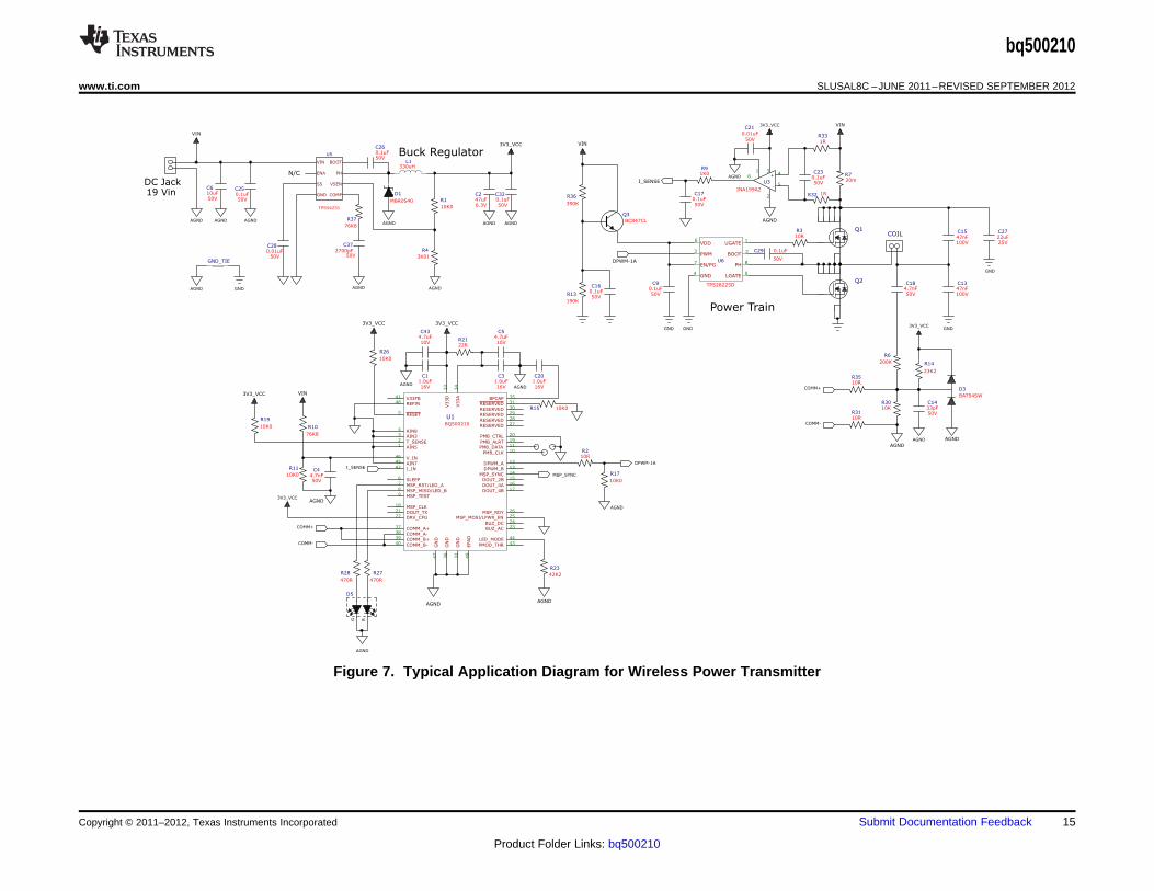
Figure 7. Typical Application Diagram for Wireless Power Transmitter
Copyright © 2011–2012, Texas Instruments Incorporated Submit Documentation Feedback 15
Product Folder Links: bq500210

bq500210
SLUSAL8C –JUNE 2011–REVISED SEPTEMBER 2012 www.ti.com
REVISION HISTORY
Changes from Original (June 2011) to Revision A Page
• Changed APPLICATION INFORMATION description ........................................................................................................ 13
• Changed Figure 6 ............................................................................................................................................................... 14
Changes from Revision A (August 2011) to Revision B Page
• Changed APPLICATION INFORMATION description ........................................................................................................ 13
• Changed Figure 6 ............................................................................................................................................................... 14
• Changed Figure 7 ............................................................................................................................................................... 15
Changes from Revision B (July 2012) to Revision C Page
• Changed Functional Block Diagram ..................................................................................................................................... 4
• Changed pinout ..................................................................................................................................................................... 5
• Changed pin 26 to MSP_RDY .............................................................................................................................................. 6
• Changed pins 27-31 to Reserved, for factory use only in PIN FUNCTIONS ....................................................................... 6
16 Submit Documentation Feedback Copyright © 2011–2012, Texas Instruments Incorporated
Product Folder Links: bq500210

PACKAGE OPTION ADDENDUM
www.ti.com 11-Apr-2013
Addendum-Page 1
PACKAGING INFORMATION
Orderable Device Status(1)
Package Type PackageDrawing
Pins PackageQty
Eco Plan(2)
Lead/Ball Finish MSL Peak Temp(3)
Op Temp (°C) Top-Side Markings(4)
Samples
BQ500210RGZR ACTIVE VQFN RGZ 48 2500 Green (RoHS& no Sb/Br)
CU NIPDAU Level-3-260C-168 HR -40 to 110 BQ500210
BQ500210RGZT ACTIVE VQFN RGZ 48 250 Green (RoHS& no Sb/Br)
CU NIPDAU Level-3-260C-168 HR -40 to 110 BQ500210
(1) The marketing status values are defined as follows:ACTIVE: Product device recommended for new designs.LIFEBUY: TI has announced that the device will be discontinued, and a lifetime-buy period is in effect.NRND: Not recommended for new designs. Device is in production to support existing customers, but TI does not recommend using this part in a new design.PREVIEW: Device has been announced but is not in production. Samples may or may not be available.OBSOLETE: TI has discontinued the production of the device.
(2) Eco Plan - The planned eco-friendly classification: Pb-Free (RoHS), Pb-Free (RoHS Exempt), or Green (RoHS & no Sb/Br) - please check http://www.ti.com/productcontent for the latest availabilityinformation and additional product content details.TBD: The Pb-Free/Green conversion plan has not been defined.Pb-Free (RoHS): TI's terms "Lead-Free" or "Pb-Free" mean semiconductor products that are compatible with the current RoHS requirements for all 6 substances, including the requirement thatlead not exceed 0.1% by weight in homogeneous materials. Where designed to be soldered at high temperatures, TI Pb-Free products are suitable for use in specified lead-free processes.Pb-Free (RoHS Exempt): This component has a RoHS exemption for either 1) lead-based flip-chip solder bumps used between the die and package, or 2) lead-based die adhesive used betweenthe die and leadframe. The component is otherwise considered Pb-Free (RoHS compatible) as defined above.Green (RoHS & no Sb/Br): TI defines "Green" to mean Pb-Free (RoHS compatible), and free of Bromine (Br) and Antimony (Sb) based flame retardants (Br or Sb do not exceed 0.1% by weightin homogeneous material)
(3) MSL, Peak Temp. -- The Moisture Sensitivity Level rating according to the JEDEC industry standard classifications, and peak solder temperature.
(4) Multiple Top-Side Markings will be inside parentheses. Only one Top-Side Marking contained in parentheses and separated by a "~" will appear on a device. If a line is indented then it is acontinuation of the previous line and the two combined represent the entire Top-Side Marking for that device.
Important Information and Disclaimer:The information provided on this page represents TI's knowledge and belief as of the date that it is provided. TI bases its knowledge and belief on informationprovided by third parties, and makes no representation or warranty as to the accuracy of such information. Efforts are underway to better integrate information from third parties. TI has taken andcontinues to take reasonable steps to provide representative and accurate information but may not have conducted destructive testing or chemical analysis on incoming materials and chemicals.TI and TI suppliers consider certain information to be proprietary, and thus CAS numbers and other limited information may not be available for release.
In no event shall TI's liability arising out of such information exceed the total purchase price of the TI part(s) at issue in this document sold by TI to Customer on an annual basis.
TAPE AND REEL INFORMATION
*All dimensions are nominal
Device PackageType
PackageDrawing
Pins SPQ ReelDiameter
(mm)
ReelWidth
W1 (mm)
A0(mm)
B0(mm)
K0(mm)
P1(mm)
W(mm)
Pin1Quadrant
BQ500210RGZR VQFN RGZ 48 2500 330.0 16.4 7.3 7.3 1.5 12.0 16.0 Q2
BQ500210RGZR VQFN RGZ 48 2500 330.0 16.4 7.3 7.3 1.5 12.0 16.0 Q2
BQ500210RGZT VQFN RGZ 48 250 180.0 16.4 7.3 7.3 1.5 12.0 16.0 Q2
BQ500210RGZT VQFN RGZ 48 250 180.0 16.4 7.3 7.3 1.5 12.0 16.0 Q2
PACKAGE MATERIALS INFORMATION
www.ti.com 8-May-2013
Pack Materials-Page 1

*All dimensions are nominal
Device Package Type Package Drawing Pins SPQ Length (mm) Width (mm) Height (mm)
BQ500210RGZR VQFN RGZ 48 2500 367.0 367.0 38.0
BQ500210RGZR VQFN RGZ 48 2500 367.0 367.0 38.0
BQ500210RGZT VQFN RGZ 48 250 210.0 185.0 35.0
BQ500210RGZT VQFN RGZ 48 250 210.0 185.0 35.0
PACKAGE MATERIALS INFORMATION
www.ti.com 8-May-2013
Pack Materials-Page 2


IMPORTANT NOTICE
Texas Instruments Incorporated and its subsidiaries (TI) reserve the right to make corrections, enhancements, improvements and otherchanges to its semiconductor products and services per JESD46, latest issue, and to discontinue any product or service per JESD48, latestissue. Buyers should obtain the latest relevant information before placing orders and should verify that such information is current andcomplete. All semiconductor products (also referred to herein as “components”) are sold subject to TI’s terms and conditions of salesupplied at the time of order acknowledgment.
TI warrants performance of its components to the specifications applicable at the time of sale, in accordance with the warranty in TI’s termsand conditions of sale of semiconductor products. Testing and other quality control techniques are used to the extent TI deems necessaryto support this warranty. Except where mandated by applicable law, testing of all parameters of each component is not necessarilyperformed.
TI assumes no liability for applications assistance or the design of Buyers’ products. Buyers are responsible for their products andapplications using TI components. To minimize the risks associated with Buyers’ products and applications, Buyers should provideadequate design and operating safeguards.
TI does not warrant or represent that any license, either express or implied, is granted under any patent right, copyright, mask work right, orother intellectual property right relating to any combination, machine, or process in which TI components or services are used. Informationpublished by TI regarding third-party products or services does not constitute a license to use such products or services or a warranty orendorsement thereof. Use of such information may require a license from a third party under the patents or other intellectual property of thethird party, or a license from TI under the patents or other intellectual property of TI.
Reproduction of significant portions of TI information in TI data books or data sheets is permissible only if reproduction is without alterationand is accompanied by all associated warranties, conditions, limitations, and notices. TI is not responsible or liable for such altereddocumentation. Information of third parties may be subject to additional restrictions.
Resale of TI components or services with statements different from or beyond the parameters stated by TI for that component or servicevoids all express and any implied warranties for the associated TI component or service and is an unfair and deceptive business practice.TI is not responsible or liable for any such statements.
Buyer acknowledges and agrees that it is solely responsible for compliance with all legal, regulatory and safety-related requirementsconcerning its products, and any use of TI components in its applications, notwithstanding any applications-related information or supportthat may be provided by TI. Buyer represents and agrees that it has all the necessary expertise to create and implement safeguards whichanticipate dangerous consequences of failures, monitor failures and their consequences, lessen the likelihood of failures that might causeharm and take appropriate remedial actions. Buyer will fully indemnify TI and its representatives against any damages arising out of the useof any TI components in safety-critical applications.
In some cases, TI components may be promoted specifically to facilitate safety-related applications. With such components, TI’s goal is tohelp enable customers to design and create their own end-product solutions that meet applicable functional safety standards andrequirements. Nonetheless, such components are subject to these terms.
No TI components are authorized for use in FDA Class III (or similar life-critical medical equipment) unless authorized officers of the partieshave executed a special agreement specifically governing such use.
Only those TI components which TI has specifically designated as military grade or “enhanced plastic” are designed and intended for use inmilitary/aerospace applications or environments. Buyer acknowledges and agrees that any military or aerospace use of TI componentswhich have not been so designated is solely at the Buyer's risk, and that Buyer is solely responsible for compliance with all legal andregulatory requirements in connection with such use.
TI has specifically designated certain components as meeting ISO/TS16949 requirements, mainly for automotive use. In any case of use ofnon-designated products, TI will not be responsible for any failure to meet ISO/TS16949.
Products Applications
Audio www.ti.com/audio Automotive and Transportation www.ti.com/automotive
Amplifiers amplifier.ti.com Communications and Telecom www.ti.com/communications
Data Converters dataconverter.ti.com Computers and Peripherals www.ti.com/computers
DLP® Products www.dlp.com Consumer Electronics www.ti.com/consumer-apps
DSP dsp.ti.com Energy and Lighting www.ti.com/energy
Clocks and Timers www.ti.com/clocks Industrial www.ti.com/industrial
Interface interface.ti.com Medical www.ti.com/medical
Logic logic.ti.com Security www.ti.com/security
Power Mgmt power.ti.com Space, Avionics and Defense www.ti.com/space-avionics-defense
Microcontrollers microcontroller.ti.com Video and Imaging www.ti.com/video
RFID www.ti-rfid.com
OMAP Applications Processors www.ti.com/omap TI E2E Community e2e.ti.com
Wireless Connectivity www.ti.com/wirelessconnectivity
Mailing Address: Texas Instruments, Post Office Box 655303, Dallas, Texas 75265Copyright © 2013, Texas Instruments Incorporated