qiuting wang design and construction of a pll system …
TRANSCRIPT

QIUTING WANG
DESIGN AND CONSTRUCTION OF A PLL SYSTEM FOR A
96-MHZ FM TRANSMITTER
Master of Science Thesis
Examiner: University Lecturer Olli-
Pekka Lundén and Lecturer Jari Kangas
Examiner and topic approved by the
Faculty Council of the Faculty of
Computing and Electrical Engineering
on 31st May 2017
I
ABSTRACT
QIUTING WANG: Design and Construction of A PLL System for A 96-MHz FMTransmitterTampere University of Technology
Master of Science Thesis, 54 pages, 3 Appendix pages
December 2017
Master's Degree Programme in Electrical Engineering
Major: Electronics
Examiner: University Lecturer Olli-Pekka Lundén and Lecturer Jari Kangas
Keywords: phase-locked loop, crystal oscillator, voltage-controlled oscillator, frequency
divider, phase detector, loop lter
The phase-locked loop (PLL) is used as frequency synthesizer in numerous electronic
devices. This thesis presents design and construction of a basic PLL system on sol-
derless breadboard, using discrete components and integrated circuits (ICs). The
circuitry is designed to synthesize a 96-MHz sinusoidal signal, which can be used as
the carrier wave for an FM transmitter. The circuitry includes a 24-MHz crystal
oscillator (XO), a 96-MHz voltage-controlled oscillator (VCO), two frequency di-
viders, a phase detector (PD), and a loop lter (LF). In addition, a buer amplier
is placed before each frequency divider for diminishing spurious frequencies. The
XO provides 24-MHz reference frequency while the VCO is tunable between 86 MHz
and 100 MHz. The constructed PLL system is able to lock the VCO frequency to
96 MHz.
In this thesis, fundamental knowledge related to PLL is reviewed, and all building
blocks of the PLL system are studied and analyzed. The challenges on utilizing IC
chips are also discussed. Therefore this work provides a guide and reference for simi-
lar works and future study. For further research, the method of eliminating spurious
frequencies and improving loop stability could be explored deeper to optimize the
PLL performance.

II
PREFACE
Although this work took longer time than expected, I feel very glad that it was
completed nally. I would like to thank my supervisors and examiners, Olli-Pekka
Lundén and Jari Kangas, for oering me so many helpful suggestions and a variety
of assistance, either on lab work or on thesis writing. I would also like to thank my
parents and friends for always supporting and encouraging me.
Tampere, 20th December 2017
Qiuting Wang

III
CONTENTS
1. Introduction . . . . . . . . . . . . . . . . . . . . . . . . . . . . . . . . . . . 1
2. Background . . . . . . . . . . . . . . . . . . . . . . . . . . . . . . . . . . . 3
2.1 Commonly used units . . . . . . . . . . . . . . . . . . . . . . . . . . . 3
2.2 The development of PLL . . . . . . . . . . . . . . . . . . . . . . . . . 4
2.2.1 The History of PLL . . . . . . . . . . . . . . . . . . . . . . . . . 4
2.2.2 The classication of PLL . . . . . . . . . . . . . . . . . . . . . . 4
2.3 The building blocks of PLL . . . . . . . . . . . . . . . . . . . . . . . 4
2.3.1 Crystal oscillators . . . . . . . . . . . . . . . . . . . . . . . . . . 5
2.3.2 Voltage-controlled oscillators . . . . . . . . . . . . . . . . . . . . 9
2.3.3 Frequency dividers . . . . . . . . . . . . . . . . . . . . . . . . . . 12
2.3.4 Phase detectors . . . . . . . . . . . . . . . . . . . . . . . . . . . . 14
2.3.5 Loop lters . . . . . . . . . . . . . . . . . . . . . . . . . . . . . . 21
2.4 The control theory of PLL and key parameters . . . . . . . . . . . . . 22
3. Block design, construction and testing . . . . . . . . . . . . . . . . . . . . 26
3.1 Crystal oscillator design, construction and testing . . . . . . . . . . . 26
3.2 Voltage-controlled oscillator design, construction and testing . . . . . 29
3.3 Frequency divider design, construction and testing . . . . . . . . . . . 34
3.4 Phase detector design, construction and testing . . . . . . . . . . . . 36
3.5 Loop lter design, construction and testing . . . . . . . . . . . . . . . 41
4. Results and analysis . . . . . . . . . . . . . . . . . . . . . . . . . . . . . . 43
4.1 Analysis of the phase detector . . . . . . . . . . . . . . . . . . . . . . 43
4.2 Analysis of the frequency divider . . . . . . . . . . . . . . . . . . . . 46
4.3 Measurement results . . . . . . . . . . . . . . . . . . . . . . . . . . . 50
5. Conclusions . . . . . . . . . . . . . . . . . . . . . . . . . . . . . . . . . . . 53
References . . . . . . . . . . . . . . . . . . . . . . . . . . . . . . . . . . . . . . 54
APPENDIX A. Measurement setups . . . . . . . . . . . . . . . . . . . . . . . 55

IV
APPENDIX B. VCO tuning range . . . . . . . . . . . . . . . . . . . . . . . . 57

V
LIST OF FIGURES
2.1 A block diagram of PLL. . . . . . . . . . . . . . . . . . . . . . . . . . 5
2.2 The concept of most electronic oscillators. . . . . . . . . . . . . . . . 5
2.3 (a) A quartz crystal and (b) the electronic symbol of quartz crystal. . 6
2.4 An equivalent circuit of quartz crystal. . . . . . . . . . . . . . . . . . 6
2.5 The magnitude of Zeq as a function of frequency f (generated by
Matlab). . . . . . . . . . . . . . . . . . . . . . . . . . . . . . . . . . . 7
2.6 A typical Pierce crystal oscillator circuit. . . . . . . . . . . . . . . . . 8
2.7 A simple crystal oscillator with transistor. . . . . . . . . . . . . . . . 8
2.8 The topology of three-point oscillator (using MOSFET), (a) with gate
grounded, (b) with drain grounded, (c) with source grounded. . . . . 9
2.9 (a) A Clapp oscillator and (b) a Clapp VCO circuit. . . . . . . . . . . 10
2.10 The characteristic of VCO output frequency. . . . . . . . . . . . . . . 11
2.11 D ip-op symbol. . . . . . . . . . . . . . . . . . . . . . . . . . . . . 12
2.12 A D ip-op composed by logic gates. . . . . . . . . . . . . . . . . . . 12
2.13 An example sequence diagram of a positive edge-triggered D ip-op. 13
2.14 (a) The diagram of a by-2 divider and (b) the sequence diagram of
by-2 divider. . . . . . . . . . . . . . . . . . . . . . . . . . . . . . . . . 13
2.15 (a) The diagram of a by-4 divider and (b) the sequence diagram of
by-4 divider. . . . . . . . . . . . . . . . . . . . . . . . . . . . . . . . . 14
2.16 A double-balanced diode mixer. . . . . . . . . . . . . . . . . . . . . . 15
2.17 The input and output waveforms of double-balanced diode mixer
when θe = 0. . . . . . . . . . . . . . . . . . . . . . . . . . . . . . . . . 15

LIST OF FIGURES VI
2.18 The input and output waveforms of double-balanced diode mixer
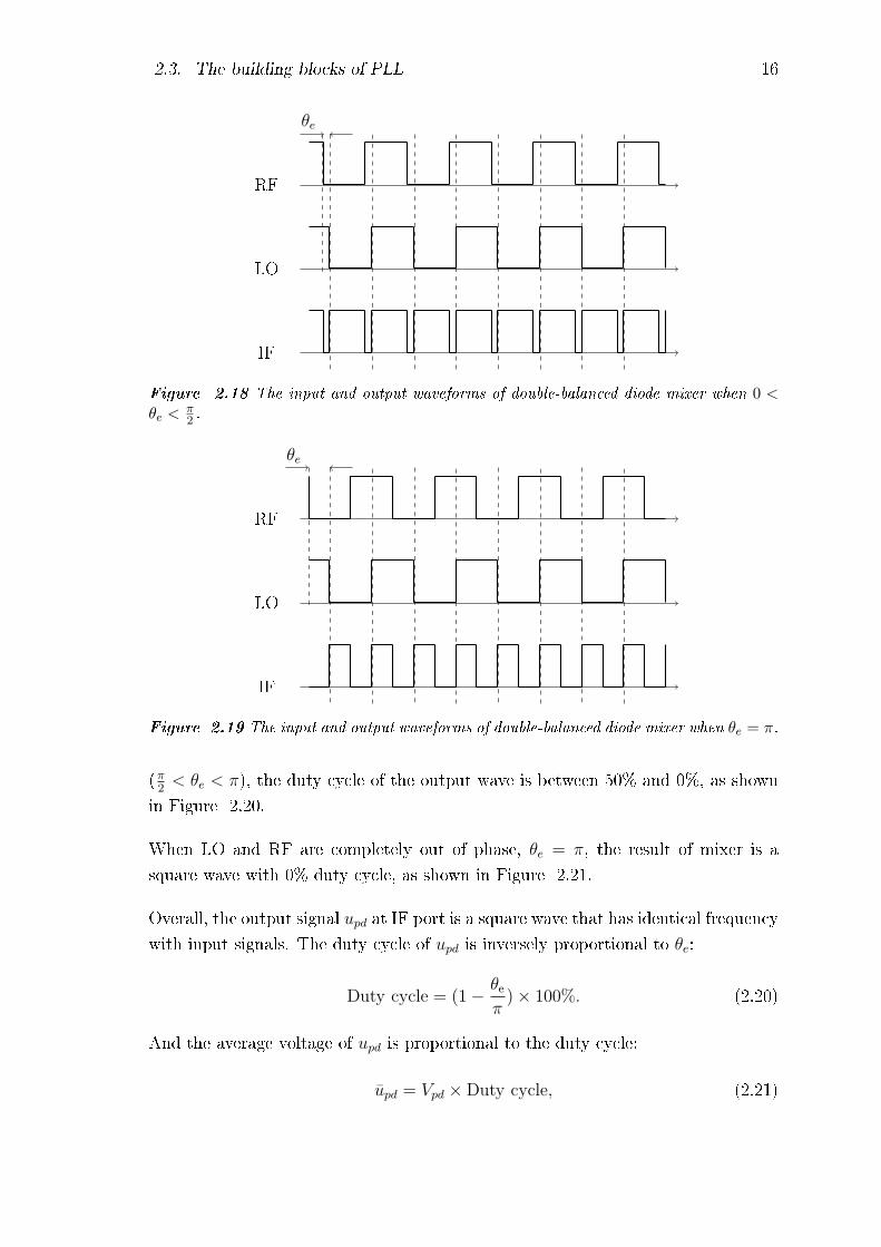
when 0 < θe <π2. . . . . . . . . . . . . . . . . . . . . . . . . . . . . . 16
2.19 The input and output waveforms of double-balanced diode mixer
when θe = π. . . . . . . . . . . . . . . . . . . . . . . . . . . . . . . . 16
2.20 The input and output waveforms of double-balanced diode mixer
when π2< θe < π. . . . . . . . . . . . . . . . . . . . . . . . . . . . . . 17
2.21 The input and output waveforms of double-balanced diode mixer
when θe = π. . . . . . . . . . . . . . . . . . . . . . . . . . . . . . . . 17
2.22 The upd as a function of θe for double-balanced mixer. . . . . . . . . . 18
2.23 Schematic symbol an XOR gate. . . . . . . . . . . . . . . . . . . . . . 18
2.24 The input and output waveform of XOR gate when θe = 0. . . . . . . 19
2.25 The input and output waveform of XOR gate when 0 < θe <π2. . . . 19
2.26 The input and output waveform of XOR gate when θe = π/2. . . . . 20
2.27 The input and output waveform of XOR gate when π2< θe < π. . . . 20
2.28 The input and output waveform of XOR gate when θe = π. . . . . . . 20
2.29 The upd as a function of θe for XOR gate. . . . . . . . . . . . . . . . . 21
2.30 An RC low-pass lter. . . . . . . . . . . . . . . . . . . . . . . . . . . 22
2.31 The modeled PLL loop showing voltages and angular frequencies. . . 22
2.32 The modeled PLL loop focused on phases. . . . . . . . . . . . . . . . 23
3.1 The block diagram of PLL system for this project. . . . . . . . . . . . 26
3.2 The designed 24-MHz crystal oscillator circuit. . . . . . . . . . . . . . 27
3.3 The redrawn crystal oscillator circuit. . . . . . . . . . . . . . . . . . . 28
3.4 The constructed 24-MHz crystal oscillator circuit. . . . . . . . . . . . 28
3.5 (a) The output signal of XO observed through oscilloscope and (b)
observed through spectrum analyzer. . . . . . . . . . . . . . . . . . . 28

LIST OF FIGURES VII
3.6 The designed 96-MHz VCO circuit. . . . . . . . . . . . . . . . . . . . 29
3.7 The diode capacitance of BYV26C as a function of its reverse voltage. 30
3.8 An air-wound coil. . . . . . . . . . . . . . . . . . . . . . . . . . . . . 30
3.9 The constructed 96-MHz VCO circuit. . . . . . . . . . . . . . . . . . 32
3.10Measurement setup for VCO test. . . . . . . . . . . . . . . . . . . . . 32
3.11 The output frequency of the VCO (fo) as a function of input control
voltage (Vctrl). . . . . . . . . . . . . . . . . . . . . . . . . . . . . . . . 32
3.12 The VCO output measured by spectrum analyzer with 2.7-V Vctrl. . . 33
3.13 The output waveform of 96-MHz VCO circuit observed through os-
cilloscope. . . . . . . . . . . . . . . . . . . . . . . . . . . . . . . . . . 33
3.14 The pin diagram of 74AC74. . . . . . . . . . . . . . . . . . . . . . . . 34
3.15 The connection diagram of by-4 divider. . . . . . . . . . . . . . . . . 35
3.16 The connection diagram of by-16 divider. . . . . . . . . . . . . . . . . 36
3.17 (a) The constructed by-4 divider for XO and (b) the constructed by-
16 divider for VCO. . . . . . . . . . . . . . . . . . . . . . . . . . . . . 36
3.18 (a) Divided XO signal and (b) divided VCO signal. . . . . . . . . . . 37
3.19 The schematic for phase detector testing. . . . . . . . . . . . . . . . . 37
3.20 The input and output waveform of phase detector. . . . . . . . . . . . 38
3.21 (a) The pinouts of CD4070BE and (b) the connection way of CD4070BE
in this project. . . . . . . . . . . . . . . . . . . . . . . . . . . . . . . 39
3.22 The constructed phase detector. . . . . . . . . . . . . . . . . . . . . . 39
3.23 The output waveform of detecting two signals of 6 MHz (seconds/di-
vision 50 ns, volts/division 2 V). . . . . . . . . . . . . . . . . . . . . . 40
3.24 The output waveform of detecting two signals of 10 kHz (seconds/di-
vision 50 µs, volts/division 2 V). . . . . . . . . . . . . . . . . . . . . . 40
3.25Measurement setup for measuring Kd. . . . . . . . . . . . . . . . . . . 40

LIST OF FIGURES VIII
3.26 The RC low-pass lter. . . . . . . . . . . . . . . . . . . . . . . . . . . 41
3.27 (a) The constructed LPF circuit and (b) the output waveform of LPF
(volts/division 500 mV, lowest line as ground level). . . . . . . . . . . 42
4.1 The diagram of SA602A. . . . . . . . . . . . . . . . . . . . . . . . . . 44
4.2 (a) The connection way of SA602A for testing, and (b) the con-
structed circuit of SA602A for testing. . . . . . . . . . . . . . . . . . 45
4.3 The output waveforms of SA602A when detecting two 1-MHz signals
(volts/division 0.5 V, seconds/division 0.5 µs, lowest line as ground
level). . . . . . . . . . . . . . . . . . . . . . . . . . . . . . . . . . . . 45
4.4 The output waveforms of CD4070BE when detecting two 1-MHz sig-
nals (volts/division 2 V, seconds/division 1 µs, lowest line as ground
level). . . . . . . . . . . . . . . . . . . . . . . . . . . . . . . . . . . . 46
4.5 The average voltage upd as a function of phase error θe for CD4070BE. 46
4.6 (a) The spectrum of VCO output when VCO works independently
and (b) the spectrum of VCO output when VCO works with divide-
by-16 circuit. . . . . . . . . . . . . . . . . . . . . . . . . . . . . . . . 47
4.7 (a) The spectrum of XO output when XO works independently and
(b) the spectrum of XO output when XO works with divide-by-4 circuit. 47
4.8 (a) The buer circuit for XO and (b) the buer circuit for VCO. . . . 48
4.9 (a) The XO with its buer and (b) the VCO with its buer. . . . . . 48
4.10 (a) The spectrum of XO working without buer and (b) the spectrum
of XO working with buer. . . . . . . . . . . . . . . . . . . . . . . . . 49
4.11 (a) The spectrum of VCO when working without buer and (b) the
spectrum of VCO when working with buer. . . . . . . . . . . . . . . 49
4.12 (a) The amplied XO output and (b) the amplied VCO output. . . 49
4.13 The block diagram of whole PLL system. . . . . . . . . . . . . . . . . 50
4.14 The completed PLL circuitry. . . . . . . . . . . . . . . . . . . . . . . 50

IX
4.15 The spectrum of VCO output at locked state: (a) with 150-MHz span
and (b) with 100-kHz span. . . . . . . . . . . . . . . . . . . . . . . . 51

X
LIST OF TABLES
2.1 The truth table of a positive triggered D ip-op. . . . . . . . . . . . 13
2.2 The truth table of an XOR gate. . . . . . . . . . . . . . . . . . . . . 18
3.1 Measured parameters of 24-MHz crystal oscillator circuit. . . . . . . . 29
3.2 Measured parameters of 96-MHz VCO circuit. . . . . . . . . . . . . . 34
3.3 The truth table of 74AC74. . . . . . . . . . . . . . . . . . . . . . . . 35
3.4 The result of detecting two 4.8-MHz square waves. . . . . . . . . . . . 41
4.1 Transition time and propagation delay time of CD4070BE. . . . . . . 43
XI
LIST OF ABBREVIATIONS AND SYMBOLS
PLL phase-locked loop
VCO voltage-controlled oscillator
FM frequency modulation
XO crystal oscillator
PD phase detector
LF loop lter
IC integrated circuit
RF radio frequency
RMS root mean square
LPLL linear phase-locked loop
DPLL digital phase-locked loop
ADPLL all-digital phase-locked loop
SPLL software phase-locked loop
APLL analog phase-locked loop
LO local oscillator
IF intermediate frequency
LPF low-pass lter
AP |dB power gain in dB
Pin input power
PL load power
AV |dB voltage gain in dB
Vin input voltage RMS value
Vout output voltage RMS value
P |dBm power in dBm
P |mW power in mW
Veff RMS value (eective value) of voltage
Vpp peak-to-peak value of voltage
ωi reference (angular) frequency
ωo VCO output (angular) frequencyωo
Ndivided VCO output (angular) frequency
upd phase detector output voltage
Vctrl VCO input control voltage
fs series resonant frequency of quartz crystal
fp parallel resonant frequency of quartz crystal
Zeq impedance of quartz crystal equivalent circuit

XII
Cvar capacitance of varactor diode
ωmax maximum VCO output frequency
ωmin minimum VCO output frequency
Kv VCO gain
∆ωV CO VCO tuning range
Kn frequency divider gain
θn frequency divider output phase
θe phase dierence between two signals
upd average voltage of upd
Kd phase detector gain
ωc cuto frequency of low-pass lter
τ time constant
Kf loop lter gain
θi XO output phase
θo VCO output phase
ωn natural frequency
ζ damping factor
ωcr lock range (capture range)
tL locking time (settling time)

1
1. INTRODUCTION
The phase-locked loop (PLL) is a feedback circuitry that can control an oscillator
signal to track a reference signal by locking the phase dierence between these two
signals into a constant. The oscillator is commonly a voltage-controlled oscillator
(VCO), and the phase dierence is detected by a phase detector. [1, p.3]
The PLL was invented in 1930s [2, p.6] and it has been extensively utilized in many
electronic elds, such as in wireless communication, microprocessor, and navigation.
A PLL system can be found for example, in FM (frequency modulation) radios,
televisions, computers, and cell phones [3, p.269].
The main applications of PLL system are reproduction of signals (as with noise
reduction), modulation and demodulation, plus frequency synthesis. [1, p.3-4] [3,
p.270-271]
A signal usually needs to be modulated before being sent out through a transmitter.
The object of this work is to design and build a PLL circuitry, which can synthesize a
96-MHz carrier frequency for the purpose of frequency modulation. This PLL system
is composed by ve building blocks: a 24-MHz crystal oscillator (XO) which oers
a reference signal, a 96-MHz VCO, two frequency dividers, a phase detector (PD),
and a loop lter (LF). The whole circuitry is constructed on solderless breadboards
with discrete components, except an IC (integrated circuit) chip CD4070BE used
as PD and three IC chips 74AC74 used as dividers. The 96-MHz output signal can
be used for an FM transmitter.
The PLL plays a preliminary but important role in radio frequency (RF) study. This
thesis reviews the concept and mechanism of the PLL, presents the construction of
each block and records their testing results, therefore providing a guide and reference
for similar works and future study. The thesis also compares and discusses the
applicability of some IC chips for the studied PLL.
This thesis is organized as follows. Chapter 2 introduces the reader to the funda-
mentals of PLL, including the development of PLL, the building blocks of PLL,
and related control theory. Chapter 3 demonstrates the design of every block, also

Chapter 1. Introduction 2
presents their constructed circuits and measurement results. Chapter 4 analyzes
some challenges on the phase detector and the frequency divider, presents the re-
sults of whole system, followed by conclusions in Chapter 5.
3
2. BACKGROUND
In this chapter, rstly some commonly used units are mentioned in Section 2.1. The
development of phase-locked loop (PLL) is introduced in Section 2.2. Then each
building block is explained separately in Section 2.3. Lastly the control theory of
PLL is demonstrated in Section 2.4.
2.1 Commonly used units
Decibels (dB) are generally used when describing power and gain [4, p.7]. The power
gain is expressed as:
AP |dB = 10 logPLPin
, (2.1)
where Pin is the input power and PL is the load power.
The voltage gain (assuming the input impedance equals the load impedance) is
expressed as:
AV |dB = 20 logVoutVin
, (2.2)
where Vin is RMS (root mean square) value of input voltage and Vout is RMS value
of output voltage.
A power level is converted into dBm as:
P |dBm = 10 logP |mW
1 mW, (2.3)
where P |mW is a power value in mW.
The RMS value (or eective value) of voltage Veff across 50-Ω load can be converted
into power value as:
P |dBm = 10 log(Veff |V)2
50 Ω × 10−3 W, (2.4)
while for a sinusoidal signal, the relationship between Veff and peak-to-peak value
of voltage Vpp is described as:
Vpp = 2√
2Veff . (2.5)
2.2. The development of PLL 4
2.2 The development of PLL
This section presents the history and classication of PLL.
2.2.1 The History of PLL
In 1932, a French engineer named Henri de Bellescize published a paper in the
French periodical L'Onde Electrique, presenting the rst PLL circuit in the world.
This PLL was built based on two vacuum tubes, for the purpose of receiving signals
synchronously. However, his work failed to attract public attention at that time. [2,
p.6-7]
After about twenty years, the PLL began to be applied as a synthesizer due to
the development of color televisions. The popularity of computers also promoted
the innovation of PLL. Nowadays, PLL has been utilized in a variety of electronic
devices. [2, p.7][5, p.8-9]
2.2.2 The classication of PLL
There are primarily four types of PLL at present: linear PLLs (LPLLs), digital PLLs
(DPLLs), all-digital PLLs (ADPLLs), and software PLLs (SPLLs). [2, p.8]
LPLLs are also referred as analog PLLs (APLLs), constructed purely by analog
components. DPLLs have gradually replaced LPLLs, since 1970's, due to their
advantages in system stability. In DPLLs, some parts of the circuitry utilize digital
elements. The third type, ADPLLs do not include any analog components. Finally,
SPLLs are implemented by software and the PLL function is realized based on
programs. [2, p.8]
This work is focusing on DPLLs, hence the following PLLs in this thesis mainly refer
to digital PLLs.
2.3 The building blocks of PLL
A primary block diagram of PLL is depicted in Figure 2.1. It consists of a crystal
oscillator (XO), a voltage-controlled oscillator (VCO), a frequency divider, a phase
detector (PD), and a loop lter (LF).
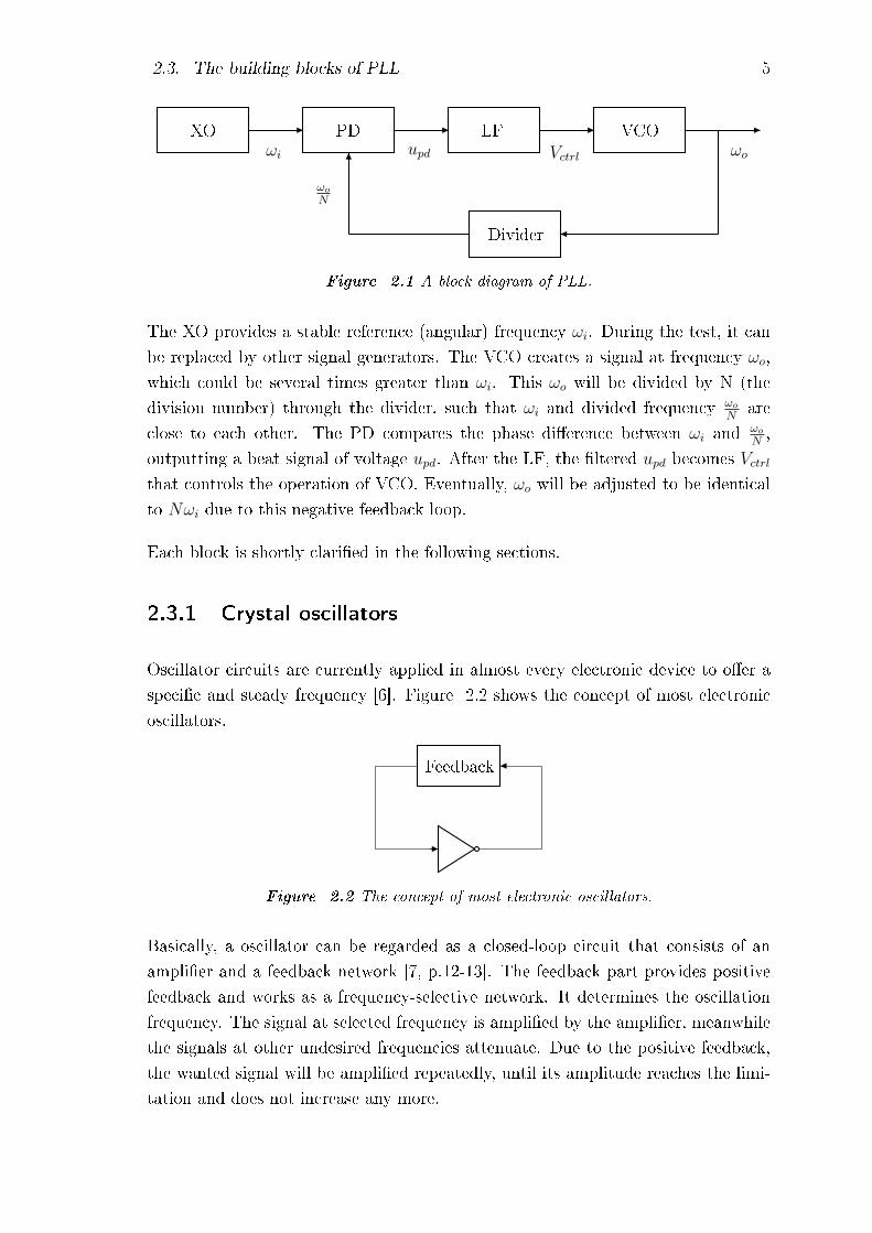
2.3. The building blocks of PLL 5
XO PD LF VCO
Divider
ωi
ωo
N
upd Vctrl ωo
Figure 2.1 A block diagram of PLL.
The XO provides a stable reference (angular) frequency ωi. During the test, it can
be replaced by other signal generators. The VCO creates a signal at frequency ωo,
which could be several times greater than ωi. This ωo will be divided by N (the
division number) through the divider, such that ωi and divided frequency ωo
Nare
close to each other. The PD compares the phase dierence between ωi andωo
N,
outputting a beat signal of voltage upd. After the LF, the ltered upd becomes Vctrl
that controls the operation of VCO. Eventually, ωo will be adjusted to be identical
to Nωi due to this negative feedback loop.
Each block is shortly claried in the following sections.
2.3.1 Crystal oscillators
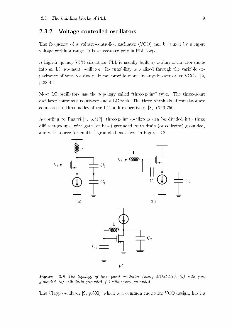
Oscillator circuits are currently applied in almost every electronic device to oer a
specic and steady frequency [6]. Figure 2.2 shows the concept of most electronic
oscillators.
Feedback
Figure 2.2 The concept of most electronic oscillators.
Basically, a oscillator can be regarded as a closed-loop circuit that consists of an
amplier and a feedback network [7, p.12-13]. The feedback part provides positive
feedback and works as a frequency-selective network. It determines the oscillation
frequency. The signal at selected frequency is amplied by the amplier, meanwhile
the signals at other undesired frequencies attenuate. Due to the positive feedback,
the wanted signal will be amplied repeatedly, until its amplitude reaches the limi-
tation and does not increase any more.

2.3. The building blocks of PLL 6
There are two necessary requirements for generating stable sinusoid. Firstly, the
total phase shift of loop equals 360. Usually the amplier provides 180 phase shift
and the feedback network provides another 180 phase shift. Secondly, the closed-
loop gain must be 1, which means the amplier gain compensates fully for the signal
attenuation in the feedback path. [4, p.502-506] [7, p.10-13]
According to the components of feedback network, oscillators can be basically di-
vided into RC oscillators, LC oscillators, crystal oscillators, and other oscillators.
The one used in this project is a crystal oscillator.
The crystal oscillator appeared in 1920's [7, p.1]. It is usually used for creating
a reference signal at a precise frequency because it usually has better frequency
stability than an RC or LC oscillator. Figure 2.3 presents a picture of quartz
(SiO2) crystal and its electronic symbol. Both two opposite sides of the thin piece
of quartz are metalized for electrical contact. Because of the piezoelectric eect,
the quartz vibrates in its thickness direction and nally generates an alternating
current at its resonant frequency. Thinner quartz has higher resonant frequency,
thereby the physical thickness of a quartz restricts its frequency upper limitation.
Commonly, the resonant frequency of a quartz crystal is made from several tens of
kHz to several tens of MHz. [7, p.3]
(a) (b)
Figure 2.3 (a) A quartz crystal and (b) the electronic symbol of quartz crystal.
LxCx Rs
Cp
Figure 2.4 An equivalent circuit of quartz crystal.
As shown in Figure 2.4, an equivalent circuit of quartz crystal includes an inductor
Lx and a capacitor Cx, that make the crystal strongly frequency-selective. There
is also a parallel capacitor Cp representing the parasitic capacitance of the metal

2.3. The building blocks of PLL 7
platings, the package, and the leads. A series resistor Rs representing the mechanical
and electrical losses. Crystal exhibits two dierent resonant frequencies: one is the
series resonant frequency (fs) caused by Lx and Cx, the other is the parallel resonant
frequency (fp) caused by Lx, Cx and Cp. These two frequencies can be calculated
from:
fs =1
2π√LxCx
, (2.6)
fp =1
2π√Lx
CxCp
Cx+Cp
. (2.7)
Supposing Lx = 4.2 H, Cx = 0.006 pF, Rs = 260 Ω, Cp = 3.4 pF (values from
[7, p.5]), fs and fp can be obtained as approximately 1.00258 and 1.00346 MHz
respectively, from Equation 2.6 and 2.7. The impedance of this equivalent circuit
Zeq can be calculated from:
Zeq = (−j2πfCp) // (j2πfLx − j2πfCx +Rs) (2.8)
Figure 2.5 The magnitude of Zeq as a function of frequency f (generated by Matlab).
Figure 2.5 plots the magnitude of Zeq as a function of frequency f . The circuit
presents low impedance at its series resonant frequency (1.00258 MHz) and high
impedance at parallel resonant frequency (1.00346 MHz). Crystal oscillators work
at the series resonant frequency. However, according to the connecting ways of
crystal, the oscillator circuits can be divided into series-resonant circuits and parallel-

2.3. The building blocks of PLL 8
resonant circuits. In a series-resonant oscillator, the crystal impedance is low at the
oscillation frequency while in a parallel-resonant oscillator, the crystal impedance is
high at the oscillation frequency. [7, p.9]
Pierce crystal oscillator (see Figure 2.6) has simple structure and good frequency
stability. Consequently, it was selected for this project. Pierce oscillator circuit
was derived from Colpitts oscillator, a parallel-resonant circuit (see Figure 2.7), by
George W. Pierce. [7, p.25-27,45-51]
XTAL
R1
OUT
C1 C2
Figure 2.6 A typical Pierce crystal oscillator circuit.
XTAL
C2
C1
R1
OUT
VCC
R2
Figure 2.7 A simple crystal oscillator with transistor.
In a Pierce crystal oscillator, it is the quartz crystal and two capacitors that form the
feedback network, determine the resonant frequency and provide 180 phase shift.
2.3. The building blocks of PLL 9
2.3.2 Voltage-controlled oscillators
The frequency of a voltage-controlled oscillator (VCO) can be tuned by a input
voltage within a range. It is a necessary part in PLL loop.
A high-frequency VCO circuit for PLL is usually built by adding a varactor diode
into an LC resonant oscillator. Its tunability is realized through the variable ca-
pacitance of varactor diode. It can provide more linear gain over other VCOs. [2,
p.38-42]
Most LC oscillators use the topology called three-point type. The three-point
oscillator contains a transistor and a LC tank. The three terminals of transistor are
connected to three nodes of the LC tank respectively. [8, p.749-750]
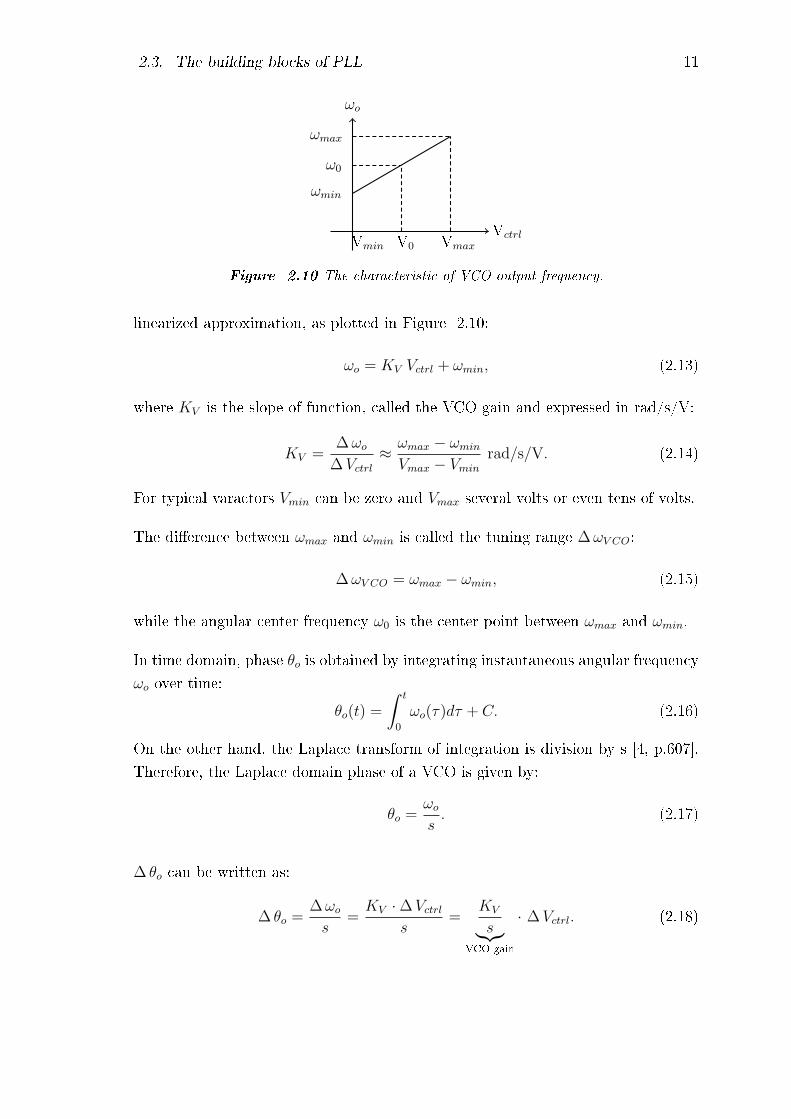
According to Razavi [4, p.517], three-point oscillators can be divided into three
dierent groups: with gate (or base) grounded, with drain (or collector) grounded,
and with source (or emitter) grounded, as shown in Figure 2.8.
L
C2
C1
Vb
(a)
L
C1 C2
Vb
(b)
C1
L
C2
(c)
Figure 2.8 The topology of three-point oscillator (using MOSFET), (a) with gategrounded, (b) with drain grounded, (c) with source grounded.
The Clapp oscillator [9, p.605], which is a common choice for VCO design, has its

2.3. The building blocks of PLL 10
drain (or collector) grounded, as shown in Figure 2.9(a). The tunable oscillator is
obtained by replacing the capacitor C0 with a varactor diode (see Figure 2.9(b)). [9,
p.606-607]
Cb
C1
C2 RL
L
C0
(a)
Cb
C1
C2 RL
L
Cvar
(b)
Figure 2.9 (a) A Clapp oscillator and (b) a Clapp VCO circuit.
The capacitance of a varactor diode Cvar decreases as its reverse-biasing voltage
increases, which can be described as followed:
Cvar = CV 0
(1− Vctrl
Vdiff
)(−1/2)
, (2.9)
where CV 0 is the original capacitance of diode without any applied voltage, Vctrl is
the applied reverse-biasing voltage, and Vdiff is the barrier voltage of the pn-junction.
[9, p.307-308]
The resonant frequency ωo of clapp VCO in Figure 2.9(b) is calculated from:
ωo =
√1
L
(1
Cvar+
1
C1
+1
C2
). (2.10)
Thereby, the maximum output frequency ωmax is calculated from:
ωmax =
√1
L
(1
Cvar_min+
1
C1
+1
C2
), (2.11)
and the minimum output frequency ωmin is calculated from:
ωmin =
√1
L
(1
Cvar_max+
1
C1
+1
C2
). (2.12)
The ωo can be described as a function of input control voltage Vctrl after a locally
2.3. The building blocks of PLL 11
Vmin V0 Vmax
Vctrl
ωmin
ω0
ωmax
ωo
Figure 2.10 The characteristic of VCO output frequency.
linearized approximation, as plotted in Figure 2.10:
ωo = KV Vctrl + ωmin, (2.13)
where KV is the slope of function, called the VCO gain and expressed in rad/s/V:
KV =∆ωo
∆Vctrl≈ ωmax − ωminVmax − Vmin
rad/s/V. (2.14)
For typical varactors Vmin can be zero and Vmax several volts or even tens of volts.
The dierence between ωmax and ωmin is called the tuning range ∆ωV CO:
∆ωV CO = ωmax − ωmin, (2.15)
while the angular center frequency ω0 is the center point between ωmax and ωmin.
In time domain, phase θo is obtained by integrating instantaneous angular frequency
ωo over time:
θo(t) =
∫ t
0
ωo(τ)dτ + C. (2.16)
On the other hand, the Laplace transform of integration is division by s [4, p.607].
Therefore, the Laplace domain phase of a VCO is given by:
θo =ωos. (2.17)
∆ θo can be written as:
∆ θo =∆ωos
=KV ·∆Vctrl
s=
KV
s︸︷︷︸VCO gain
· ∆Vctrl. (2.18)

2.3. The building blocks of PLL 12
2.3.3 Frequency dividers
A frequency divider divides an input frequency usually by an integer. There are
analog dividers and digital dividers: analog dividers are targeted at very high fre-
quencies, while digital dividers are commonly used in IC chips. [4, p.655-661]
The ip-op divider is a digital divider. Flip-ops [10, p.142] are bistable circuits
meaning that it can ip between state 0 (logic low level) and 1 (logic high level)
under the eect of its input signal. Flip-op dividers have the advantages of simple
structure, low power consumption, and low cost. [10, p.143-145]
The D ip-op (data ip-op, or delay ip-op) is popular for frequency division.
It is an edge triggered ip-op, which means the stored state will ip at the positive
edge or the negative edge of input clock signal.
D
CLK
Q
Q
Figure 2.11 D ip-op symbol.
As shown in Figure 2.11, a D ip-op has two input nodes and two output nodes:
data input D, clock input CLK, output Q and its complement Q. Q and Q are
opposite to each other. A D ip-op can be made by connecting logic gates in the
way shown in Figure 2.12, using four NAND gates with one NOT gate.
Q
Q
CLK
D
Figure 2.12 A D ip-op composed by logic gates.
Table 2.1 shows the truth table of a positive edge-triggered D ip-op. Qn is the
previous state of Qn+1. In brief, the output Q takes the state of data input only
when CLK jumps from low to high. In any other cases, Q and Q remain their
previous value no matter which state D is, because the stored memory is latched. If
the ip-op is negative triggered, the output values will ip at negative edges. This
edge triggered ip-ops help to reject the interference and reduce the possibility of

2.3. The building blocks of PLL 13
error, because the output will hold its state except the moment of triggering even if
there are interferences at input D.
Table 2.1 The truth table of a positive triggered D ip-op.
CLK D Qn+1 Qn+1
↑ 0 0 1
↑ 1 1 0
↓ × Qn Qn
0 × Qn Qn
1 × Qn Qn
Figure 2.13 shows an example sequence diagram of a positive edge-triggered D
ip-op, designed with Xilinx ISE (a VHDL design tool).
Figure 2.13 An example sequence diagram of a positive edge-triggered D ip-op.
A by-2 divider can be obtained by connecting the Q of D ip-op to its D. Figure
2.14 presents a by-2 divider and its corresponding sequence diagram created with
Xilinx ISE.
D
CLK
Q
Qfin fout
(a)
(b)
Figure 2.14 (a) The diagram of a by-2 divider and (b) the sequence diagram of by-2divider.
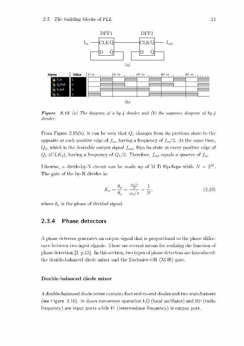
Similarly, a by-4 divider can be implemented by cascading two D ip-op, as depicted
in Figure 2.15(a). The input signal goes into the CLK pin of rst ip-op, then its
Q is connected to the CLK of second ip-op.
2.3. The building blocks of PLL 14
D
CLK
Q
Qfin fout
D
CLK
Q
Q
DFF1 DFF2
(a)
(b)
Figure 2.15 (a) The diagram of a by-4 divider and (b) the sequence diagram of by-4divider.
From Figure 2.15(b), it can be seen that Q1 changes from its previous state to the
opposite at each positive edge of fin, having a frequency of fin/2. At the same time,
Q2, which is the desirable output signal fout, ips its state at every positive edge of
Q1 (CLK2), having a frequency of Q1/2. Therefore, fout equals a quarter of fin.
Likewise, a divide-by-N circuit can be made up of M D ip-ops while N = 2M .
The gain of the by-N divider is:
Kn =θnθo
=ωo/sN
ωo/s=
1
N, (2.19)
where θn is the phase of divided signal.
2.3.4 Phase detectors
A phase detector generates an output signal that is proportional to the phase dier-
ence between two input signals. There are several means for realizing the function of
phase detection [2, p.15]. In this section, two types of phase detectors are introduced:
the double-balanced diode mixer and the Exclusive-OR (XOR) gate.
Double-balanced diode mixer
A double-balanced diode mixer contains four end-to-end diodes and two transformers
(see Figure 2.16). In down conversion operation LO (local oscillator) and RF (radio
frequency) are input ports while IF (intermediate frequency) is output port.

2.3. The building blocks of PLL 15
RF
IF
LO
Figure 2.16 A double-balanced diode mixer.
Two input ports are fed with strong enough square waves at same frequency. When
LO signal is positive, the upper two diodes conduct current and lower two diodes are
o. Therefore, RF signal ows from the upper terminal of its secondary side into IF,
which means the IF reproduce the signal of RF. When LO signal is negative, there
is the opposite situation. The lower two diodes conduct current instead, and RF
signal ows from the lower terminal into IF. In this case, the IF signal is the negative
of RF. Figures 2.17 - 2.21 illustrate how the double-balanced mixer detects two
square waves.
When LO and RF are in phase, the phase dierence between them is 0 (θe = 0), the
result of mixer is a square wave with 100% duty cycle, see Figure 2.17.
RF
LO
IF
Figure 2.17 The input and output waveforms of double-balanced diode mixer when θe = 0.
When the phase dierence between LO and RF is higher than 0 but lower than π/2
(0 < θe <π2), the duty cycle of the output wave is between 100% and 50%, as shown
in Figure 2.18.
When the phase dierence between LO and RF is exactly π/2 (θe = π), the result
of mixer is a square wave with 50% duty cycle, as shown in Figure 2.19.
When the phase dierence between LO and RF is higher than π/2 but lower than π
2.3. The building blocks of PLL 16
RF
LO
IF
θe
Figure 2.18 The input and output waveforms of double-balanced diode mixer when 0 <θe <
π2 .
RF
LO
IF
θe
Figure 2.19 The input and output waveforms of double-balanced diode mixer when θe = π.
(π2< θe < π), the duty cycle of the output wave is between 50% and 0%, as shown
in Figure 2.20.
When LO and RF are completely out of phase, θe = π, the result of mixer is a
square wave with 0% duty cycle, as shown in Figure 2.21.
Overall, the output signal upd at IF port is a square wave that has identical frequency
with input signals. The duty cycle of upd is inversely proportional to θe:
Duty cycle = (1− θeπ
)× 100%. (2.20)
And the average voltage of upd is proportional to the duty cycle:
upd = Vpd ×Duty cycle, (2.21)

2.3. The building blocks of PLL 17
RF
LO
IF
θe
Figure 2.20 The input and output waveforms of double-balanced diode mixer when π2 <
θe < π.
RF
LO
IF
Figure 2.21 The input and output waveforms of double-balanced diode mixer when θe = π.
where Vpd is the amplitude of upd.
Therefore, upd can be written as a function of θe:
upd = Vpd × (1− θeπ
). (2.22)
The relationship between θe and upd is plotted in Figure 2.22. It is a periodical
triangle wave with period of 2π. The slope at −π2is also called the gain of this phase
detector, which is calculated from:
Kd =∆ upd∆ θe
=Vpdπ. (2.23)

2.3. The building blocks of PLL 18
0π2 π−π
2−π 3π2 2π−3π
2−2π
upd
θe
Vpd
Figure 2.22 The upd as a function of θe for double-balanced mixer.
Exclusive-OR gate
The Exclusive-OR (XOR) gate is a simple logic gate, usually represented as shown
in Figure 2.23. According to its truth table shown in Table 2.2, if input A and
B are dierent, the XOR gate generates a logic 1, otherwise the output Q will be
logic 0.
A
B
Q
Figure 2.23 Schematic symbol an XOR gate.
Table 2.2 The truth table of an XOR gate.
A B Q
0 0 0
0 1 1
1 0 1
1 1 0
Figures 2.24 - 2.28 depict the output waveforms of XOR gate when comparing two
square waves of identical frequency. Basically, they are opposite to the results of
double-balanced mixer. [2, p.52-55]
When θe = 0, the result of XOR gate is shown in Figure 2.24. The duty cycle of
square wave equals 0%.
When 0 < θe <π2, see Figure 2.25, the duty cycle of the output is lower than 50%.

2.3. The building blocks of PLL 19
A
B
Q
Figure 2.24 The input and output waveform of XOR gate when θe = 0.
A
B
Q
θe
Figure 2.25 The input and output waveform of XOR gate when 0 < θe <π2 .
When θe = π/2, the result of XOR gate is shown in Figure 2.26. The duty cycle of
square wave is exactly 50%.
When π2< θe < π, see Figure 2.27, the duty cycle of the output is higher than 50%.
When θe = π, two input signals are completely out of phase, the waveform is shown
in Figure 2.28. The duty cycle of square wave reaches 100%.
The relationship between upd and θe can be described as:
upd = Vpd ×θeπ. (2.24)
Figure 2.29 presents the upd as a function of θe for XOR gate. Maximum upd is
achieved when input waves are out of phase by π, and minimum upd is obtained

2.3. The building blocks of PLL 20
A
B
Q
θe
Figure 2.26 The input and output waveform of XOR gate when θe = π/2.
A
B
Q
θe
Figure 2.27 The input and output waveform of XOR gate when π2 < θe < π.
A
B
Q
Figure 2.28 The input and output waveform of XOR gate when θe = π.
2.3. The building blocks of PLL 21
0π2 π−π
2−π 3π2 2π−3π
2−2π
upd
θe
Vpd
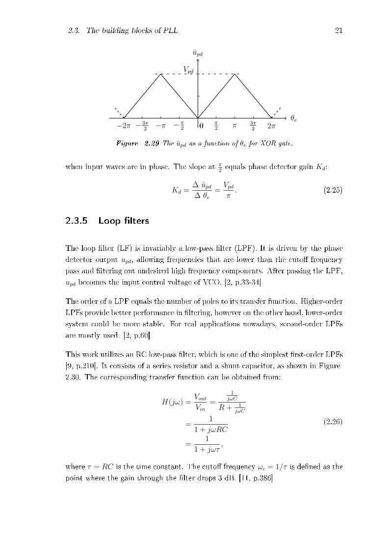
Figure 2.29 The upd as a function of θe for XOR gate.
when input waves are in phase. The slope at π2equals phase detector gain Kd:
Kd =∆ upd∆ θe
=Vpdπ. (2.25)
2.3.5 Loop lters
The loop lter (LF) is invariably a low-pass lter (LPF). It is driven by the phase
detector output upd, allowing frequencies that are lower than the cuto frequency
pass and ltering out undesired high frequency components. After passing the LPF,
upd becomes the input control voltage of VCO. [2, p.33-34]
The order of a LPF equals the number of poles to its transfer function. Higher-order
LPFs provide better performance in ltering, however on the other hand, lower-order
system could be more stable. For real applications nowadays, second-order LPFs
are mostly used. [2, p.60]
This work utilizes an RC low-pass lter, which is one of the simplest rst-order LPFs
[9, p.210]. It consists of a series resistor and a shunt capacitor, as shown in Figure
2.30. The corresponding transfer function can be obtained from:
H(jω) =VoutVin
=
1jωC
R + 1jωC
=1
1 + jωRC
=1
1 + jωτ,
(2.26)
where τ = RC is the time constant. The cuto frequency ωc = 1/τ is dened as the
point where the gain through the lter drops 3 dB. [11, p.386]
2.4. The control theory of PLL and key parameters 22
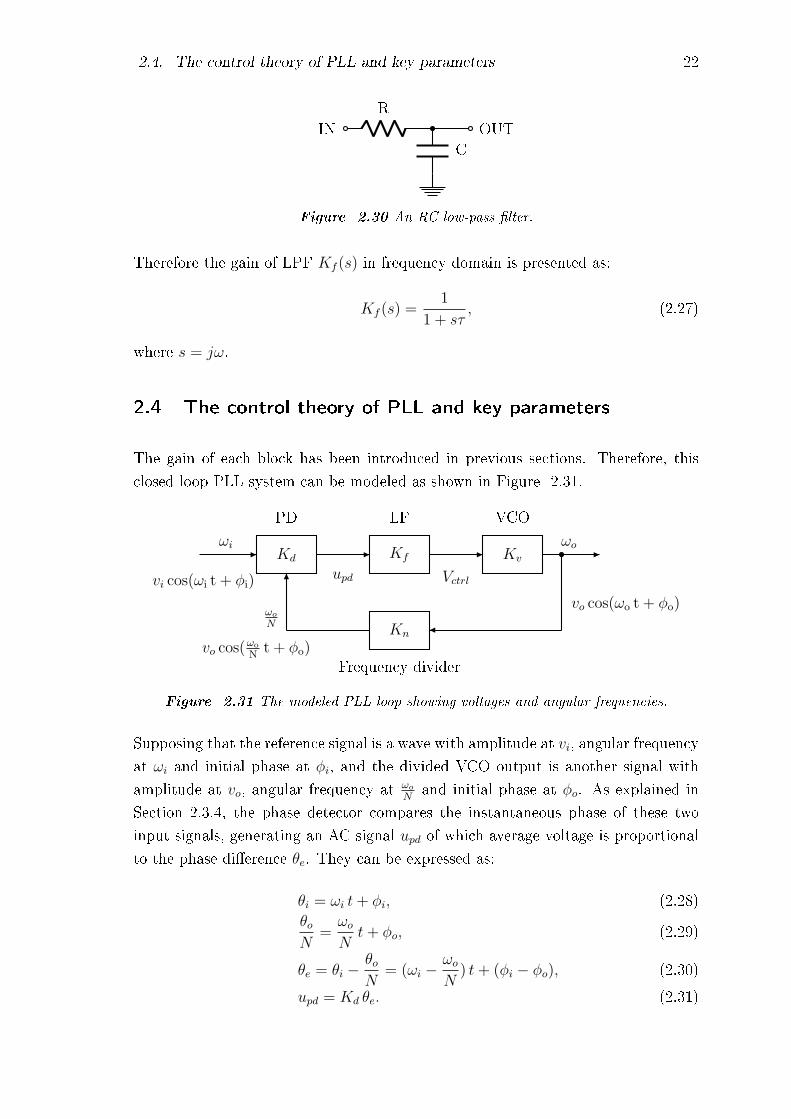
R
C
IN OUT
Figure 2.30 An RC low-pass lter.
Therefore the gain of LPF Kf (s) in frequency domain is presented as:
Kf (s) =1
1 + sτ, (2.27)
where s = jω.
2.4 The control theory of PLL and key parameters
The gain of each block has been introduced in previous sections. Therefore, this
closed-loop PLL system can be modeled as shown in Figure 2.31.
Kd Kf Kv
Kn
PD LF VCO
Frequency dividervo cos(ωo
Nt + φo)
vi cos(ωi t + φi)
vo cos(ωo t + φo)
upd Vctrl
ωi ωo
ωo
N
Figure 2.31 The modeled PLL loop showing voltages and angular frequencies.
Supposing that the reference signal is a wave with amplitude at vi, angular frequency
at ωi and initial phase at φi, and the divided VCO output is another signal with
amplitude at vo, angular frequency at ωo
Nand initial phase at φo. As explained in
Section 2.3.4, the phase detector compares the instantaneous phase of these two
input signals, generating an AC signal upd of which average voltage is proportional
to the phase dierence θe. They can be expressed as:
θi = ωi t+ φi, (2.28)
θoN
=ωoNt+ φo, (2.29)
θe = θi −θoN
= (ωi −ωoN
) t+ (φi − φo), (2.30)
upd = Kd θe. (2.31)

2.4. The control theory of PLL and key parameters 23
After passing LF, upd is ltered and integrated, becoming a DC signal Vctrl, provided
that ωi equals ωo/N . It tunes the VCO and determines the output frequency ωo.
Vctrl = Kf Kd θe, (2.32)
ωo = KvKf Kd θe + ωmin. (2.33)
If there is a dierence in ωi andωo
Nat the beginning, θe would change from 0 to
2π periodically, therefore making Vctrl also beat between Vmax and Vmin. It causes
the ωo swing between ωmax and ωmin. Meanwhile this variation of ωo is fed back
to phase detector, changing θe and tuning the VCO again continuously. Eventually
the VCO generates an exactly same frequency as Nωi, θe becomes a constant, and
the loop achieves locked state at this time.
There are two necessary requirements for locking the loop: ωo
Nequals ωi and θe
reaches a proper constant. During the settlement process, if frequency ωo
Nis equal
to ωi but θe is improper, ωo may keep changing. The loop would not be locked until
both two requirements are met. [4, p.604-605]
In this project, θe is supposed to equal π/2 when PLL is locked, because only at
this time the control voltage Vctrl reaches the center point, making the VCO create
its center frequency, which is about 96 MHz.
As nal constant θe is independent of the initial phases φi and φo, it can be assumed
that both φi and φo are equal to 0, so that the reference signal becomes vi cos(θi)
while the VCO output becomes vo cos(θo). The loop block diagram is then modied
as shown in Figure 2.32.
Kd Kf Kv/s
Kn
PD LF VCO
Frequency dividervo cos(
θoN
)
vi cos(θi)
vo cos(θo)
upd Vctrl
θi θo
θoN
Figure 2.32 The modeled PLL loop focused on phases.
Hence, the output phase of VCO is obtained as:
θo =Kv
sKf Kd (θi −Kn θo), (2.34)

2.4. The control theory of PLL and key parameters 24
and the closed-loop transfer function is given by:
H(s) =θoθi
=KdKf Kv
s+KnKdKf Kv
, (2.35)
where the gains of the phase detector, the lter, the VCO and the divider are:
Kd =∆V
πV/rad, (2.36)
Kf =1
1 + sτ, (2.37)
Kv =∆ω
∆Vrad/s/V, (2.38)
Kn =1
N. (2.39)
When the loop is locked, the divided frequency tracks the reference frequency, that
is to say:d θid t
=dKn θod t
. (2.40)
In order to analyze the stability of this system, the poles of closed-loop can be found
from:
s+KnKdKf Kv = 0
⇒ s = −1
1+sτKdKv
N
= − 1
2τ±
√(1
2τ
)2
− KdKv
τ Nrad/s.
(2.41)
According to the Nyquist stability criterion, the loop is unstable if the number of
poles located in the right-half complex plane is not equal to zero.
The order number of a PLL equals the order number of the loop lter plus 1. This
work applies simple rst-order loop lter, hence it is a second-order PLL system,
which is to say, the loop has two poles: one from LPF and the other one from VCO.
Both two poles are supposed to be in the left-half plane.
The corresponding natural frequency ωn and damping factor ζ are obtained from:
ωn =
√KdKv ωc
Nrad/s, (2.42)
ζ =ωc
2ωn. (2.43)

2.4. The control theory of PLL and key parameters 25
Normally, ζ is selected to be between 1/√
2 and 1, to avoid damped or over-damped
problems. [4, p.608]
Lock range ωcr (also known as capture range) and locking time tL (also known as
settling time) are important parameters for analyzing this kind of traditional PLL
system. The lock range means the loop is able to get locked rapidly within this
frequency range. The lock time refers to the time that system needs to achieve
locked state. [2, p.70-72]
Values of ωcr and tL are calculated from [2, p.101]:
ωcr =√N KdKv ωc rad/s, (2.44)
tL ≈2π
ωns. (2.45)

26
3. BLOCK DESIGN, CONSTRUCTION AND
TESTING
Figure 3.1 shows the block diagram of this project. A 24-MHz sine-wave from crystal
oscillator (XO) is divided by 4, while the output signal of 96-MHz voltage-controlled
oscillator (VCO) is divided by 16. Two divided frequencies are compared by phase
detector (PD), generating a signal that is proportional to the phase dierence. This
signal is then ltered by low-pass lter (LPF) and becomes the input control voltage
of VCO.
÷4
÷16
24-MHz XO
Divider
XOR-Gate PD
LPF
96-MHz VCO
RF Output
Divider
Figure 3.1 The block diagram of PLL system for this project.
The detailed design, construction and testing for each block are discussed in this
chapter. The information on measurement setups can be found in Appendix.
3.1 Crystal oscillator design, construction and testing
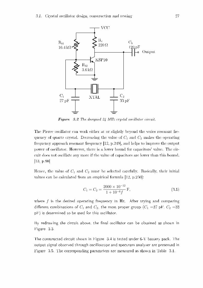
A 24-MHz quartz crystal oscillator circuit is chosen for providing a stable reference
signal at around 24 MHz. The circuit (see Figure 3.2) is designed based on Pierce
oscillator (see Figure 2.6 in Section 2.3.1). An NPN-type bipolar junction transistor
KSP10 works as the inverting amplier, providing 180 phase shift. A 24-MHz
quartz and capacitors C1 and C2 work as the feedback network, providing another
180 phase shift. Potentiometer Rb and resistor Rc are used for transistor biasing.
Capacitor Cb is used for DC block.
3.1. Crystal oscillator design, construction and testing 27
XTAL C2
33 pFC1
27 pF
Cb120 pF
Rc
220 ΩRb1
16.4 kΩ
Rb2
3.6 kΩ
Output
VCC
KSP10
Figure 3.2 The designed 24-MHz crystal oscillator circuit.
The Pierce oscillator can work either at or slightly beyond the series resonant fre-
quency of quartz crystal. Decreasing the value of C1 and C2 makes the operating
frequency approach resonant frequency [12, p.249], and helps to improve the output
power of oscillator. However, there is a lower bound for capacitors' value. The cir-
cuit does not oscillate any more if the value of capacitors are lower than this bound.
[13, p.90]
Hence, the value of C1 and C2 must be selected carefully. Basically, their initial
values can be calculated from an empirical formula [12, p.250]:
C1 = C2 =2000× 10−12
1 + 10−6fF, (3.1)
where f is the desired operating frequency in Hz. After trying and comparing
dierent combinations of C1 and C2, the most proper group (C1 =27 pF, C2 =33
pF) is determined to be used for this oscillator.
By redrawing the circuit above, the nal oscillator can be obtained as shown in
Figure 3.3.
The constructed circuit shown in Figure 3.4 is tested under 6-V battery pack. The
output signal observed through oscilloscope and spectrum analyzer are presented in
Figure 3.5. The corresponding parameters are measured as shown in Table 3.1.

3.1. Crystal oscillator design, construction and testing 28
C1
27 pF
Rb1
16.4 kΩ
Rb2
3.6 kΩ
C2
33 pF
Rc
220 Ω
XTAL
Cb120 pF
Output
VCC
KSP10
Figure 3.3 The redrawn crystal oscillator circuit.
Figure 3.4 The constructed 24-MHz crystal oscillator circuit.
(a) (b)
Figure 3.5 (a) The output signal of XO observed through oscilloscope and (b) observedthrough spectrum analyzer.
3.2. Voltage-controlled oscillator design, construction and testing 29
Table 3.1 Measured parameters of 24-MHz crystal oscillator circuit.
Parameter Value
f (Frequency) 24.04 MHz
Vpp across open circuit 6.375 V
Vpp across 50-Ω load 1.72 V
Current consumption 11.24 mA
3.2 Voltage-controlled oscillator design, construction and test-
ing
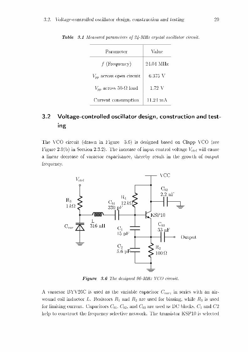
The VCO circuit (drawn in Figure 3.6) is designed based on Clapp VCO (see
Figure 2.9(b) in Section 2.3.2). The increase of input control voltage Vctrl will cause
a linear decrease of varactor capacitance, thereby result in the growth of output
frequency.
R1
12 kΩ
R2
100 Ω
Cvar
R3
1 kΩ
Vctrl
Output
VCC
KSP10
316 nHL
330 pFCb1
5.6 pFC2
15 pFC1 33 nF
Cb3
Cb22.2 nF
Figure 3.6 The designed 96-MHz VCO circuit.
A varactor BYV26C is used as the variable capacitor Cvar, in series with an air-
wound coil inductor L. Resistors R1 and R2 are used for biasing, while R3 is used
for limiting current. Capacitors Cb1, Cb2, and Cb3 are used as DC blocks, C1 and C2
help to construct the frequency selective network. The transistor KSP10 is selected
3.2. Voltage-controlled oscillator design, construction and testing 30
again as amplier.
To determine the value of capacitors and inductor, it is required to decide the
minimum output frequency ωmin and maximum output frequency ωmax at rst. In
this case the desired center frequency is 96 MHz, which is to say, the ideal VCO
circuit is supposed to generate a signal at frequency between 86 MHz and 106MHz
if the bandwidth could reach 20 MHz.
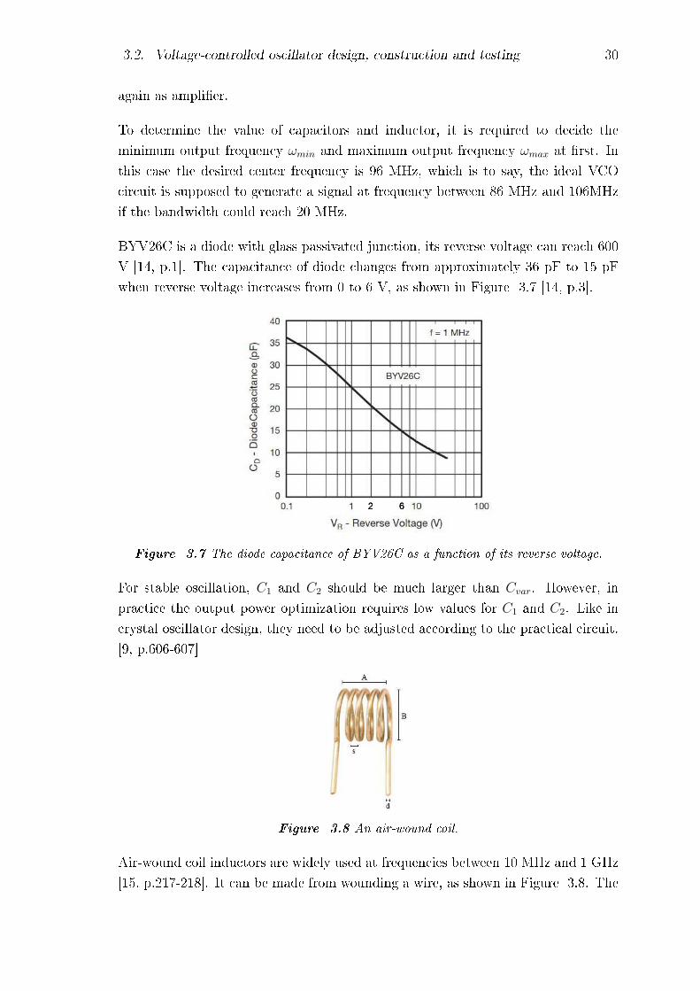
BYV26C is a diode with glass passivated junction, its reverse voltage can reach 600
V [14, p.1]. The capacitance of diode changes from approximately 36 pF to 15 pF
when reverse voltage increases from 0 to 6 V, as shown in Figure 3.7 [14, p.3].
Figure 3.7 The diode capacitance of BYV26C as a function of its reverse voltage.
For stable oscillation, C1 and C2 should be much larger than Cvar. However, in
practice the output power optimization requires low values for C1 and C2. Like in
crystal oscillator design, they need to be adjusted according to the practical circuit.
[9, p.606-607]
Figure 3.8 An air-wound coil.
Air-wound coil inductors are widely used at frequencies between 10 MHz and 1 GHz
[15, p.217-218]. It can be made from wounding a wire, as shown in Figure 3.8. The

3.2. Voltage-controlled oscillator design, construction and testing 31
value of coil inductor L can be computed from Equation 2.11 and 2.12 (see Section
2.3.2), when capacitors are known. Then the inductor size can be decided based on
the Wheeler Equation 3.2 [15, p.218].
L =B2n2
0.45B + A, (3.2)
where L is the inductance of coil in nH, B is the average diameter of coil in mm, n
is the number of turns, A is the length of coil in mm. For the coil inductor applied
in this work, A = 11, B = 10, n = 7, so the calculated L equals 316 nH.
However, an air-wound coil also has parasitic capacitance as other types of inductors,
which is supposed to be taken into consideration. As discussed in [15, p.219], the
distributed capacitance C in pF per turn is calculated from:
C ≈ Bεeff
11.45 cosh−1 sd
, (3.3)
where εeff is the eective dielectric constant between turns, s is the spacing between
turns at wire centers in mm, and d is the diameter of wire in mm. For the inductor
in this work, s = 2.2, d = 0.7, εeff ≈ 8.85 × 10¹² F/m. The calculated capacitance
per turn is about 0.09 pF.
Nevertheless, the total parasitic capacitance is not simply the series of each C be-
cause of the existing of coupling among nonadjacent turns [15, p.219]. Consequently,
it is hard to obtain an accurate real parasitic capacitance. This parasitic capacitance
will result in the decrease of VCO output frequency ωo. For this reason, the values
of C1 and C2 may have to be tuned in the actual circuit. In the end, C1 was 15 pF
and C2 was 5.6 pF.
The constructed 96-MHz VCO circuit shown in Figure 3.9 is powered from a 5-V
DC power supply. The output frequency fo is recorded when input control voltage
Vctrl ranges from 0 to 6V, as depicted in Figure 3.10. Recorded results are listed in
Appendix, and the characteristic is plotted in Figure 3.11.
This VCO is tunable between 86 MHz and 100 MHz with maximum 6-V Vctrl. In
addition, the gain of VCO (Kv) slightly decreases during the growth of Vctrl. The
desired center frequency 96 MHz is obtained with 2.7-V Vctrl (see Figure 3.12).
Figure 3.13 presents a clean output waveform observed through oscilloscope. The
measured parameters are listed in Table 3.2.

3.2. Voltage-controlled oscillator design, construction and testing 32
Figure 3.9 The constructed 96-MHz VCO circuit.
VCO
500-MHz Oscilloscope
HP 54615B
Spectrum analyzer
HP 8594E
0∼30 V DCPower supplyTL 3035
Figure 3.10 Measurement setup for VCO test.
Figure 3.11 The output frequency of the VCO (fo) as a function of input control voltage(Vctrl).

3.2. Voltage-controlled oscillator design, construction and testing 33
Figure 3.12 The VCO output measured by spectrum analyzer with 2.7-V Vctrl.
Figure 3.13 The output waveform of 96-MHz VCO circuit observed through oscilloscope.
The average VCO gain Kv is computed from:
Kv =∆ω
∆V=
2π · 14 MHz
6V= 2π · 2.33 MHz/V. (3.4)
The maximum Kv is obtained from:
Kv|0∼0.5V =∆ω
∆V=
2π · 4.25 MHz
0.5V= 2π · 8.5 MHz/V. (3.5)
The Kv around center point is obtained from:
Kv|2.5∼3V =∆ω
∆V=
2π · 0.85 MHz
0.5V= 2π · 1.7 MHz/V. (3.6)

3.3. Frequency divider design, construction and testing 34
Table 3.2 Measured parameters of 96-MHz VCO circuit.
Parameter Value
ωmin 2π·86 MHz
ωmax 2π·100 MHz
Vpp across open circuit 1.812 V
Vpp across 50-Ω load 1.11 V
Current consumption 13 mA
3.3 Frequency divider design, construction and testing
74AC74 is an IC chip that integrates two D-type positive edge-triggered ip-ops.
As shown in Figure 3.14, it has 14 pins in total, containing two data inputs D1,
D2, two clock pulse inputs CP1, CP2, four outputs Q1, Q1, Q2, Q2, two direct clear
inputs CD1, CD2 and two direct set inputs SD1, SD2, which enable the chip. Table
3.3 presents its truth table. The clear and set inputs are connected to logic high
during the test. [16]
Figure 3.14 The pin diagram of 74AC74.
As mentioned in Section 2.3.3, a divide-by-2N circuit can be realized by cascading N
D ip-ops. In this work, two 74AC74 ICs are cascaded to divide VCO output by
16 while another 74AC74 is used to divide XO output by 4. Figures 3.15 and 3.16
present the connection diagrams. R1 and R2 are used to ensure that the DC level
of input signals equals the center point of supply voltage, otherwise the IC may be
unable to work.
The maximum clock frequency of 74AC74 under 5-V power supply is expected to

3.3. Frequency divider design, construction and testing 35
Table 3.3 The truth table of 74AC74.
SD CD CP D Qn+1 Qn+1
L H × × H L
H L × × L H
L L × × H H
H H ↑ H H L
H H ↑ L L H
H H L × Qn Qn
R1
10 kΩR2
10 kΩ
VCC
OUT
IN
1 2 3 4 5 6 7
891011121314
Figure 3.15 The connection diagram of by-4 divider.
reach 125 MHz [16]. When powered by 5-V DC voltage, a by-4 divider is able
to handle input frequencies from about 930 kHz to 125 MHz, except 12∼13 MHz.
According to the test results, the recommended input power of clock signal for
driving the divider is above 12 dBm (approximately 2.5-V peak-to-peak). The chip
can handle most clock frequencies lower than 125 MHz with such amplitude. Higher
input power would be required if clock frequency approaches the limitation. In
addition, the measured current consumption of one IC is 11.5 mA.
It is noticeable that all input signals in previous tests are sinusoidal waves. The
divider would present better performance, for instance, covering greater frequency
range and requiring lower input power when it is fed by a clean square wave, because
square wave spends shorter time to transit from logic low to high.
The constructed divide-by-4 and divide-by-16 circuits shown in Figure 3.17 are
tested under 6-V battery pack. The upper left pin is connected to power supply
and lower right pin is connected to ground for all chips. In by-16 divider, two 10-nF

3.4. Phase detector design, construction and testing 36
R1
10 kΩR2
10 kΩ
VCC
OUT
IN
1 2 3 4 5 6 7
891011121314
1 2 3 4 5 6 7
891011121314
Figure 3.16 The connection diagram of by-16 divider.
capacitors are placed between power supply pin and ground pin for ltering.
(a) (b)
Figure 3.17 (a) The constructed by-4 divider for XO and (b) the constructed by-16 dividerfor VCO.
As presented in Figure 3.18, both the divided XO output and VCO output have
correct frequency, though containing high-frequency harmonies.
3.4 Phase detector design, construction and testing
The phase detector plays a vital role in PLL circuits. As mentioned in Section 2.3.4,
there are several options for realizing phase detection. In this project, both double-
balanced mixer and Exclusive-OR (XOR) gate have been tested, and the XOR gate
is selected in the end. The detailed comparison will be discussed in Chapter 4. In
brief, the average voltage of double-balanced mixer output signal has limited range,
while the XOR gate has the drawback of frequency limitation.

3.4. Phase detector design, construction and testing 37
(a) (b)
Figure 3.18 (a) Divided XO signal and (b) divided VCO signal.
The simulation of detecting two dierent frequencies by XOR gate is done with
Multisim. The schematic is shown in Figure 3.19 and a part of waveforms is
presented in Figure 3.20. The XOR gate compares a 100-Hz square wave and a
90-Hz square wave, which are indicated by green and light blue waves respectively
in the gure. The red wave represents the output of XOR gate before RC low-pass
lter while the dark blue wave represents the ltered output. It is obvious that the
red one is a periodical signal of which frequency equals the dierence between two
inputs (10 Hz). In addition, the duty cycle of square wave changes regularly from
0% to 100% then back to 0%, causing the instantaneous voltage of ltered signal
beat between maximum and minimum slowly.
5V 5V
1 kΩ
5µFXOR
OUT
100Hz 90Hz
Figure 3.19 The schematic for phase detector testing.
The nal design for this project is to detect two 6-MHz input signals using a chip
CD4070BE. CD4070 Series (manufactured by Texas Instruments) are cheap and
usual CMOS IC chips. The package of CD4070BE is PDIP, suitable for breadboard.
As shown in Figure 3.21(a), it has 14 pins, contains 4 XOR gates in total. However,
only one XOR gate is used in this project.
The IC is connected as presented in Figure 3.21(b). The capacitors are used for
ltering and resistors help maintain a proper DC level. Pin 14 and pin 7 are con-
nected to VCC and GND respectively. Pin 5 and pin 6 are connected to input while

3.4. Phase detector design, construction and testing 38
Figure 3.20 The input and output waveform of phase detector.
pin 4 is the output. Other pins are not connected. [17]
The constructed phase detector shown in Figure 3.22 is powered by 6-V DC power
supply. The upper left pin is connected to supply voltage and lower right pin is
connected to ground. A 4.7-µF capacitor is placed between these two pins for
ltering.
The output waveform of detecting two signals of 6 MHz is shown in Figure 3.23. It
appears as a sine-wave more than square wave at around 6 MHz.
For comparison, much lower frequencies are detected. Figure 3.24 shows the output
waveform of detecting two signals of 10 kHz, it is approaching a square wave. It can
be concluded that the transition and propagation delay of internal circuitry may
inuence the performance of IC, determine the upper limitation of its operating
frequency as well.
The gain Kd is measured by means of changing the phase dierence θe and record-
ing the corresponding average output voltage upd, as shown in Figure 3.25. Two
input waves are obtained by splitting a signal from function generator to ensure the
frequencies are identical. Dierent electrical lengths of the cable results in dierent
phase, so θe can be modied by changing the length of cable or changing the source
frequency. The output waveform of detecting two square waves at about 4.8 MHz
are presented in Table 3.4. The reason why 6-MHz signals were not used but 4.8-
MHz signals, instead, was a 50-m long cable provides around 90 phase dierence
at 4.8 MHz.

3.4. Phase detector design, construction and testing 39
(a)
C1
8.2 nF
C2
8.2 nF
R3
100 kΩ
R4
100 kΩ
R1
100 kΩ
R2
100 kΩ
VCC
OUT
IN1
IN2
1 2 3 4 5 6 7
891011121314
(b)
Figure 3.21 (a) The pinouts of CD4070BE and (b) the connection way of CD4070BE inthis project.
Figure 3.22 The constructed phase detector.

3.4. Phase detector design, construction and testing 40
Figure 3.23 The output waveform of detecting two signals of 6 MHz (seconds/division50 ns, volts/division 2 V).
Figure 3.24 The output waveform of detecting two signals of 10 kHz (seconds/division50 µs, volts/division 2 V).
Phasedetector
NI VirtualBench
Function generator
40-MHz Oscilloscope
KENWOOD CS-5135
Figure 3.25 Measurement setup for measuring Kd.

3.5. Loop lter design, construction and testing 41
Table 3.4 The result of detecting two 4.8-MHz square waves.
θe (in Degrees) upd (in Volts)
87 1.8
88 2.4
Therefore Kd is computed from:
Kd =∆ upd∆ θe
V/rad
=2.4− 1.8
88− 87· 180
πV/rad
≈ 34 V/rad
(3.7)
During the test, it is also found that the amplitude of input signals should keep the
same level with supply voltage, otherwise the IC will work improperly. The measured
current consumption of CD4070BE is about 9 mA under 6-V power supply.
3.5 Loop lter design, construction and testing
The simple rst-order RC low-pass lter (LPF) is selected for this work to lter
unwanted high-frequency components and let low frequency pass.
100Ω
10 nF
IN OUT
Figure 3.26 The RC low-pass lter.
The resistor R and capacitor C may be changed according to the practical circuitry
to achieve a best performance for PLL loop. The nal decided components for this
lter are a 100-Ω resistor and a 10-nF capacitor.
3.5. Loop lter design, construction and testing 42
The cuto frequency ωc of designed LPF in Figure 3.26 and its gain are given by:
ωc =1
RCrad/s = 1 MHz, (3.8)
fc =1
2πRCHz ≈ 159 kHz, (3.9)
Kf =1
1 + s · 10−6. (3.10)
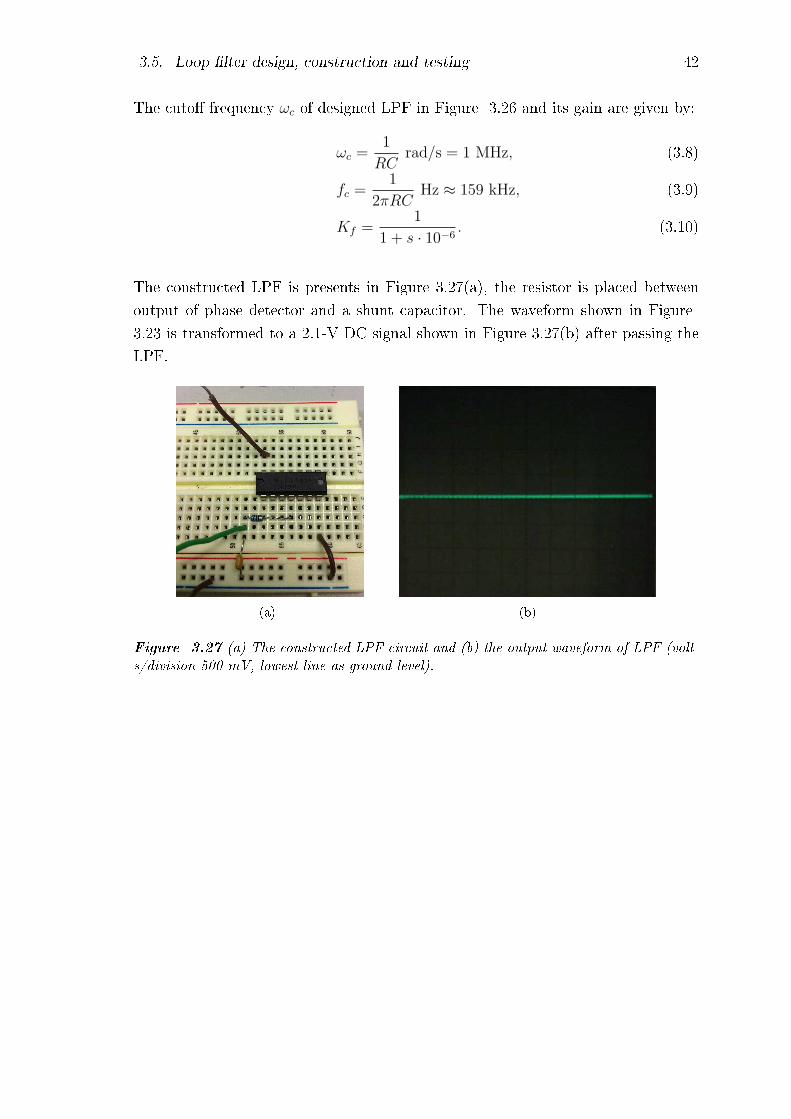
The constructed LPF is presents in Figure 3.27(a), the resistor is placed between
output of phase detector and a shunt capacitor. The waveform shown in Figure
3.23 is transformed to a 2.1-V DC signal shown in Figure 3.27(b) after passing the
LPF.
(a) (b)
Figure 3.27 (a) The constructed LPF circuit and (b) the output waveform of LPF (volt-s/division 500 mV, lowest line as ground level).

43
4. RESULTS AND ANALYSIS
This chapter discusses the challenges encountered during this work and correspond-
ing solutions to them, and presents the measurement results. Sections 4.1 and 4.2
provide the analysis on the phase detector and the frequency divider, respectively.
Section 4.3 shows the results of whole system. The information on measurement
setups is presented in Appendix.
4.1 Analysis of the phase detector
The initial idea is to divide the VCO output by 4, obtaining a frequency which
is tunable between around 21.5 MHz and 25 MHz. The XOR gate phase detector
is expected to compare this divided signal directly with 24-MHz XO output. As
shown in Figures 2.24 - 2.28, XOR gate is supposed to generate a square wave
of which duty cycle changes between 0% and 100%. However, the IC CD4070BE
has a drawback of insucient operation speed. Even though its datasheet does not
present the information related to its maximum operating frequency, the parameters
of transition time and propagation delay time can be found, as presented in Table
4.1 [17, p.5].
Table 4.1 Transition time and propagation delay time of CD4070BE.
Parameter VDD(V) Typical Maximum Units
5 100 200 ns
tTHL, tTLH 10 50 100 ns
15 40 80 ns
5 140 280 ns
tPHL, tPLH 10 65 130 ns
15 50 100 ns
VDD is the supply voltage of IC, tTHL and tTLH represent the required time that
output signal transits between logic high and low, tPHL and tPLH represent the
4.1. Analysis of the phase detector 44
required time that the signal propagates from input to output. Besides, input tr
and tf represent the time that input signal changes between logic high and low.
They are specied to be 20 ns. Basically the propagation delay time tPHL and tPLH
are not taken into consideration, because it does not aect the shape of output
waveform. Supposing the output signal falls down as soon as it rises up, becoming
a triangle wave. The output frequency under 5-V supply voltage is:
f = 1/T = 1/200 ns = 5 MHz, (4.1)
based on typical value of transition time. The upper limitation frequency would
fall down to 2.5 MHz if transition time reaches its maximum. This frequency can
be improved with higher supply voltage. However, it may not exceed 10 MHz even
under 10-V supply voltage. Obviously, it is impossible to handle 24-MHz signal for
this XOR gate.
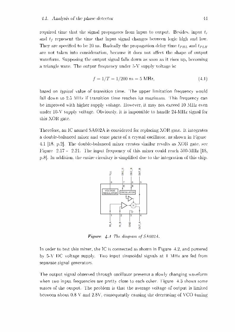
Therefore, an IC named SA602A is considered for replacing XOR gate. It integrates
a double-balanced mixer and some parts of a crystal oscillator, as shown in Figure
4.1 [18, p.2]. The double-balanced mixer creates similar results as XOR gate, see
Figure 2.17 - 2.21. The input frequency of this mixer could reach 500-MHz [18,
p.8]. In addition, the entire circuitry is simplied due to the integration of this chip.
Figure 4.1 The diagram of SA602A.
In order to test this mixer, the IC is connected as shown in Figure 4.2, and powered
by 5-V DC voltage supply. Two input sinusoidal signals at 1 MHz are fed from
separate signal generators.
The output signal observed through oscillator presents a slowly changing waveform
when two input frequencies are pretty close to each other. Figure 4.3 shows some
states of the output. The problem is that the average voltage of output is limited
between about 0.8 V and 2.8V, consequently causing the decreasing of VCO tuning

4.1. Analysis of the phase detector 45
10 nF
VCC
OUTIN1
IN2
1 2 3 4
5678
(a) (b)
Figure 4.2 (a) The connection way of SA602A for testing, and (b) the constructed circuitof SA602A for testing.
range. This result is independent on either supply voltage or input amplitude.
Figure 4.3 The output waveforms of SA602A when detecting two 1-MHz signals (volts/-division 0.5 V, seconds/division 0.5 µs, lowest line as ground level).
Another idea is to keep using CD4070BE, but adding additional frequency dividers
to scale both XO frequency and VCO frequency down to 6 MHz.
Two 1-MHz sinusoidal waves are fed from signal generators into CD4070BE for
testing. As presented in Figure 4.4, the duty cycle slowly changes from 0 to 100%
then back to 0, therefore the average output voltage is changeable between 0 V and
around 7V under 7-V supply voltage.
However, since 6-MHz is close to upper limitation frequency of chip, the performance
is not as good as at lower frequency. As can be seen from Figure 3.23 and 3.24,
when duty cycle is around 50%, the output waveform at 10 kHz looks more like
a square wave than at 6 MHz. The reason is that the frequency of 6 MHz is too
high to allow the output maintain logic high or low for longer time. The slope at
point of θe = π/2 gets steeper, and correspondingly, Kd is increased, as plotted in
Figure 4.5. Nonetheless, it is not wise to add more frequency dividers because more

4.2. Analysis of the frequency divider 46
Figure 4.4 The output waveforms of CD4070BE when detecting two 1-MHz signals (volt-s/division 2 V, seconds/division 1 µs, lowest line as ground level).
spurious frequencies will be introduced.
0π2 π−π
2−π 3π2 2π−3π
2−2π
upd
θe
umax
Figure 4.5 The average voltage upd as a function of phase error θe for CD4070BE.
Either CD4070BE or SA602A has drawback for this PLL system. Although the
CD4070BE is decided to be applied as nal design in this work, it cannot be recom-
mended for frequency detection above 2.5 MHz.
4.2 Analysis of the frequency divider
When the VCO block was connected with divide-by-16 circuit, it was found that the
divider brought VCO output signal spurious frequencies, as shown in Figure 4.6.
Similar problem happened with the by-4 divider. The spectrum of crystal oscillator
output had single frequency component, while additional spurious components were
introduced after being connected with divide-by-4 circuit, see Figure 4.7.
Several ways has been tried for the purpose of solving this problem. For example,
each block was enclosed by foils for preventing electromagnet interference. However
it was proved to be useless for eliminating the noise. Finally, these spurious signals
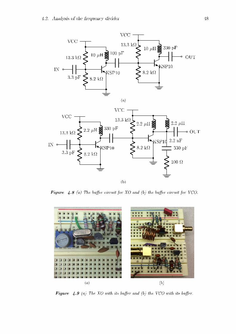
were suppressed by means of putting cascaded simple ampliers as buers at the
forward path of dividers. This method prohibits signals leak from dividers back to
previous circuit. The design of buer circuits are presented in Figure 4.8 while the

4.2. Analysis of the frequency divider 47
(a) (b)
Figure 4.6 (a) The spectrum of VCO output when VCO works independently and (b) thespectrum of VCO output when VCO works with divide-by-16 circuit.
(a) (b)
Figure 4.7 (a) The spectrum of XO output when XO works independently and (b) thespectrum of XO output when XO works with divide-by-4 circuit.
constructed circuits are shown in Figure 4.9. In VCO's buer, the series connected
2.2-µH inductor, 330-pF capacitor and 100-Ω resistor are placed before the output
port, in order to stabilize the operation of its previous transistor.
The XO output presents better frequency spectrum after adding the buer circuit,
as shown in Figure 4.10. The maximum of spurious decreases from -25 dBm (about
0.036 V Vpp) to -48 dBm (about 0.003 V Vpp).
Similarly, Figure 4.11 compares the output spectrum of VCO when it works without
and with the buer circuit. The maximum of spurious decreases from -7.65 dBm
(about 0.262 V Vpp) to -46 dBm (about 0.003 V Vpp).
Both XO and VCO output signals are amplied after passing their buer circuits,
as presented in Figure 4.12.
4.2. Analysis of the frequency divider 48
13.3 kΩ10 µH
8.2 kΩ3.3 pF
100 pF10 µH
8.2 kΩ
330 pF
VCC
KSP10IN
OUT
KSP10
VCC
13.3 kΩ
(a)
13.3 kΩ2.2 µH
8.2 kΩ3.3 pF
330 pF2.2 µH
8.2 kΩ
2.2 nF
2.2 µH
330 pF
100 Ω
VCC
KSP10IN
OUT
KSP10
VCC
13.3 kΩ
(b)
Figure 4.8 (a) The buer circuit for XO and (b) the buer circuit for VCO.
(a) (b)
Figure 4.9 (a) The XO with its buer and (b) the VCO with its buer.

4.2. Analysis of the frequency divider 49
(a) (b)
Figure 4.10 (a) The spectrum of XO working without buer and (b) the spectrum of XOworking with buer.
(a) (b)
Figure 4.11 (a) The spectrum of VCO when working without buer and (b) the spectrumof VCO when working with buer.
(a) (b)
Figure 4.12 (a) The amplied XO output and (b) the amplied VCO output.
4.3. Measurement results 50
4.3 Measurement results
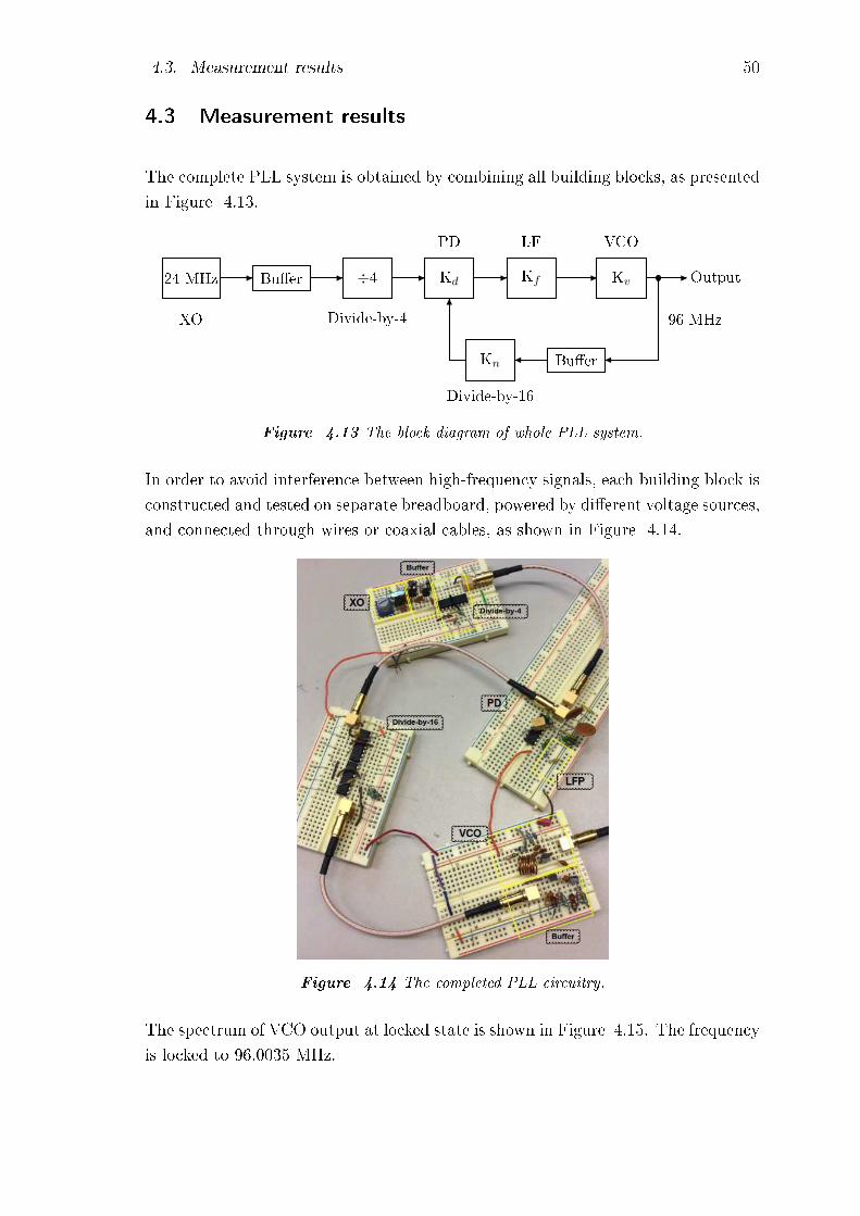
The complete PLL system is obtained by combining all building blocks, as presented
in Figure 4.13.
24 MHz
XO
Buer ÷4
Divide-by-4
Kd
PD
Kf
LF
Kv
VCO
BuerKn
Divide-by-16
Output
96 MHz
Figure 4.13 The block diagram of whole PLL system.
In order to avoid interference between high-frequency signals, each building block is
constructed and tested on separate breadboard, powered by dierent voltage sources,
and connected through wires or coaxial cables, as shown in Figure 4.14.
Figure 4.14 The completed PLL circuitry.
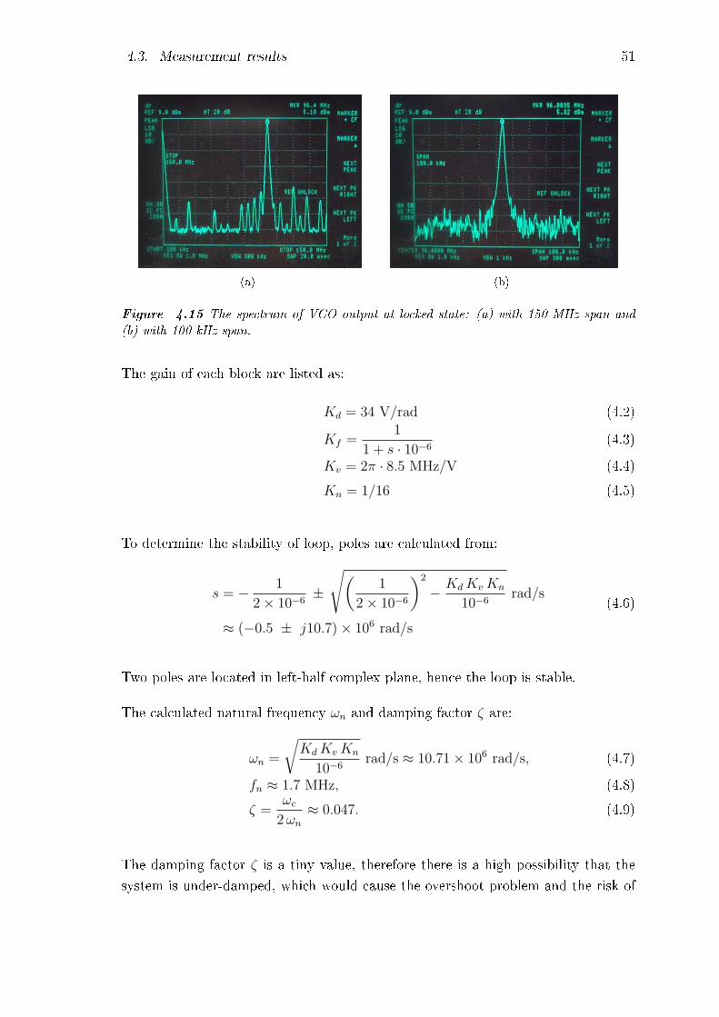
The spectrum of VCO output at locked state is shown in Figure 4.15. The frequency
is locked to 96.0035 MHz.
4.3. Measurement results 51
(a) (b)
Figure 4.15 The spectrum of VCO output at locked state: (a) with 150-MHz span and(b) with 100-kHz span.
The gain of each block are listed as:
Kd = 34 V/rad (4.2)
Kf =1
1 + s · 10−6(4.3)
Kv = 2π · 8.5 MHz/V (4.4)
Kn = 1/16 (4.5)
To determine the stability of loop, poles are calculated from:
s = − 1
2× 10⁻⁶±
√(1
2× 10⁻⁶
)2
− KdKvKn
10−6rad/s
≈ (−0.5 ± j10.7)× 106 rad/s
(4.6)
Two poles are located in left-half complex plane, hence the loop is stable.
The calculated natural frequency ωn and damping factor ζ are:
ωn =
√KdKvKn
10−6rad/s ≈ 10.71× 10⁶ rad/s, (4.7)
fn ≈ 1.7 MHz, (4.8)
ζ =ωc
2ωn≈ 0.047. (4.9)
The damping factor ζ is a tiny value, therefore there is a high possibility that the
system is under-damped, which would cause the overshoot problem and the risk of

4.3. Measurement results 52
instability. The best way to improve damping factor in this case could be decrease
the phase detector gain Kd.
The approximate values for lock range ωcr (also known as capture range) and locking
time tL (also known as settling time) are:
ωcr =
√KdKv × 106
Kn
rad/s ≈ 171.4× 10⁶ rad/s, (4.10)
fcr =ωcr2π
= 27.28 MHz, (4.11)
tL ≈2π
ωns ≈ 0.587 µs. (4.12)

53
5. CONCLUSIONS
A PLL system was designed and built on breadboard in this work, for the purpose
of synthesizing a stable carrier wave at 96 MHz. The system contains ve building
blocks: a 24-MHz crystal oscillator (XO), a 96-MHz voltage-controlled oscillator
(VCO), two frequency dividers, a phase detector (PD), and a loop lter (LF). The
XO oers a 24-MHz sine-wave as the reference signal. The VCO output frequency
can be tuned from 86 MHz to 100 MHz. The XO frequency is divided by 4 into 6
MHz, meanwhile the VCO frequency is divided by 16. The divided VCO frequency
varies accordingly between 5.375 MHz and 6.25 MHz. Two divided frequencies
are compared by a phase detector, creating a signal that is proportional to phase
dierence of these two input signals. After ltered by low-pass lter, the output of
phase detector becomes the input control voltage of VCO. The VCO frequency is
tuned to be more and more close to quadruple frequency of XO, eventually locking
exactly to 96 MHz.
During the lab work, some problems of applying IC chips are discovered and studied.
Their solutions are also presented. Additional dividers are used to decrease the in-
put frequency of phase detector CD4070BE, to compensate its insucient operation
speed. However, this XOR gate IC is problematic for frequencies above 2.5 MHz.
On the other hand, the divider 74AC74 introduces a large amount of spurious to
its previous circuit. The buer circuit which is composed by two cascaded ampli-
ers is placed at the forward path of frequency divider, in order to limit spurious
frequencies.
The constructed loop circuitry can lock to 96 MHz as expected, though there exists
a possibility of overshoot. For further research, the method of eliminating spurious
frequencies could be explored deeper to improve the practical results. Other divider
IC chips could be applied instead of 74AC74, for example, a prescaler SAB6456 can
divide a frequency by 256. It provides a larger division number than a 74AC74, and
is more compact so that it saves space. It also generates purer output waveform.
Besides, other phase detectors with higher operation speed could be implemented in-
stead of CD4070BE, to decrease the gain of phase detector, consequently improving
the stability of system and preventing under-damped problem.
54
REFERENCES
[1] William F. Egan, Phase-Lock Basics, Second Edition, John Wiley & Sons, 2008.
[2] Roland E. Best, Phase-Locked Loops: Design, Simulation, and Applications,
Sixth Edition, McGraw-Hill Education, 2007.
[3] Karl D. Stephan, Analog and Mixed-Signal Electronics, First Edition, John
Wiley & Sons, 2015.
[4] Behzad Razavi, RF Microelectronics, Second Edition, Person Education, 2012.
[5] Stanley J. Goldman, Phase-Locked Loop Engineering Handbook for Integrated
Circuits, Artech House, 2007.
[6] Martin Snelgrove, Oscillator, AccessScience, McGraw-Hill Education, 2014.
[7] Robert J. Matthys, Crystal Oscillator Circuits, Revised Edition, Krieger Pub-
lishing Company, 1992.
[8] Richard C. Li, RF Circuit Design, John Wiley & Sons, 2012.
[9] Reinhold Ludwig, Gene Bogdanov, RF Circuit Design: Theory & Applications,
Second Edition, Person Education, 2009.
[10] Brian Holdsworth, Clive Woods, Digital Logic Design, Elsevier Science, 2002.
[11] Marc Thompson, Intuitive Analog Circuit Design, Elsevier Incorporated, 2006.
[12] Randall W. Rhea, Oscillator Design and Computer Simulation, Second Edition,
SciTech Publishing, 1995.
[13] Olli-Pekka Lundén, Kristian Konttinen, Masoumeh Hasani, A simple closed-
form analysis of clapp oscillator output power using a novel quasi-linear tran-
sistor model, 2014 IEEE Radio and Wireless Symposium (RWS), 2014.
[14] BYV26C Data Sheet, Vishay Semiconductors, 2017.
[15] Peter Vizmuller, RF Design Guide: Systems, Circuits and Equations, Artech
House, 1995.
[16] 74AC74 Data Sheet, Fairchild Semiconductor Corporation, 1988.
[17] CD4070B Data Sheet, Texas Instruments Incorporated, 2003.
[18] SA602A Data Sheet, NXP Semiconductors, 2014.

55
APPENDIX A. MEASUREMENT SETUPS
The information on measurement setups are presented as follow.
For Figures 3.5, 3.18: measurement setup type A is applied.
DUT
500-MHz Oscilloscope
HP 54615B
Spectrum analyzer
HP 8594E
Figure A.1 Measurement setup type A.
For Figures 3.23, 4.3, 4.4 : measurement setup type B is applied.
Phasedetector
40-MHz Oscilloscope
KENWOOD CS-5135
Digital signal generator
HP ESG-D3000A
Digital signal generator
HP 8648C
NI VirtualBench
Mixed signal oscilloscope
Figure A.2 Measurement setup type B.
For Figure 3.24, : measurement setup type C is applied.
For Figure 3.27(b) : measurement setup type D is applied.
For Figures 4.6, 4.7, : measurement setup type E is applied.
For Figures 4.10, 4.11, 4.12: measurement setup type F is applied.

APPENDIX A. Measurement setups 56
Phasedetector
500-MHz Oscilloscope
HP 54615B
Digital signal generator
HP ESG-D3000A
Digital signal generator
HP 8648C
NI VirtualBench
Mixed signal oscilloscope
Figure A.3 Measurement setup type C.
DUT
40-MHz Oscilloscope
KENWOOD CS-5135
Spectrum analyzer
HP 8594E
Figure A.4 Measurement setup type D.
XO/
VCODivider
500-MHz Oscilloscope
HP 54615B
Spectrum analyzer
HP 8594E
Figure A.5 Measurement setup type E.
XO/
VCOBuer Divider
500-MHz Oscilloscope
HP 54615B
Spectrum analyzer
HP 8594E
Figure A.6 Measurement setup type F.

57
APPENDIX B. VCO TUNING RANGE
Table 1 The measured tuning range of 96-MHz VCO circuit.
Vctrl (V) fo (MHz)0 860.1 87.50.2 88.30.3 89.050.4 89.750.5 90.250.6 90.650.7 91.050.8 91.450.9 91.81.0 92.21.1 92.51.2 92.81.3 93.051.4 93.351.5 93.61.6 93.81.7 94.01.8 94.251.9 94.452.0 94.72.5 95.62.7 96.03.0 96.453.5 97.24.0 97.84.5 98.455.0 99.05.5 99.56.0 100