qlogic isp1040b scsi i/o processor - smithsonian...
TRANSCRIPT

Construction Analysis
Qlogic ISP1040BSCSI I/O Processor
Report Number: SCA 9710-557
®
Serv
ing
the
Global Semiconductor Industry
Since1964
17350 N. Hartford DriveScottsdale, AZ 85255Phone: 602-515-9780Fax: 602-515-9781
e-mail: [email protected]: http://www.ice-corp.com
- i -
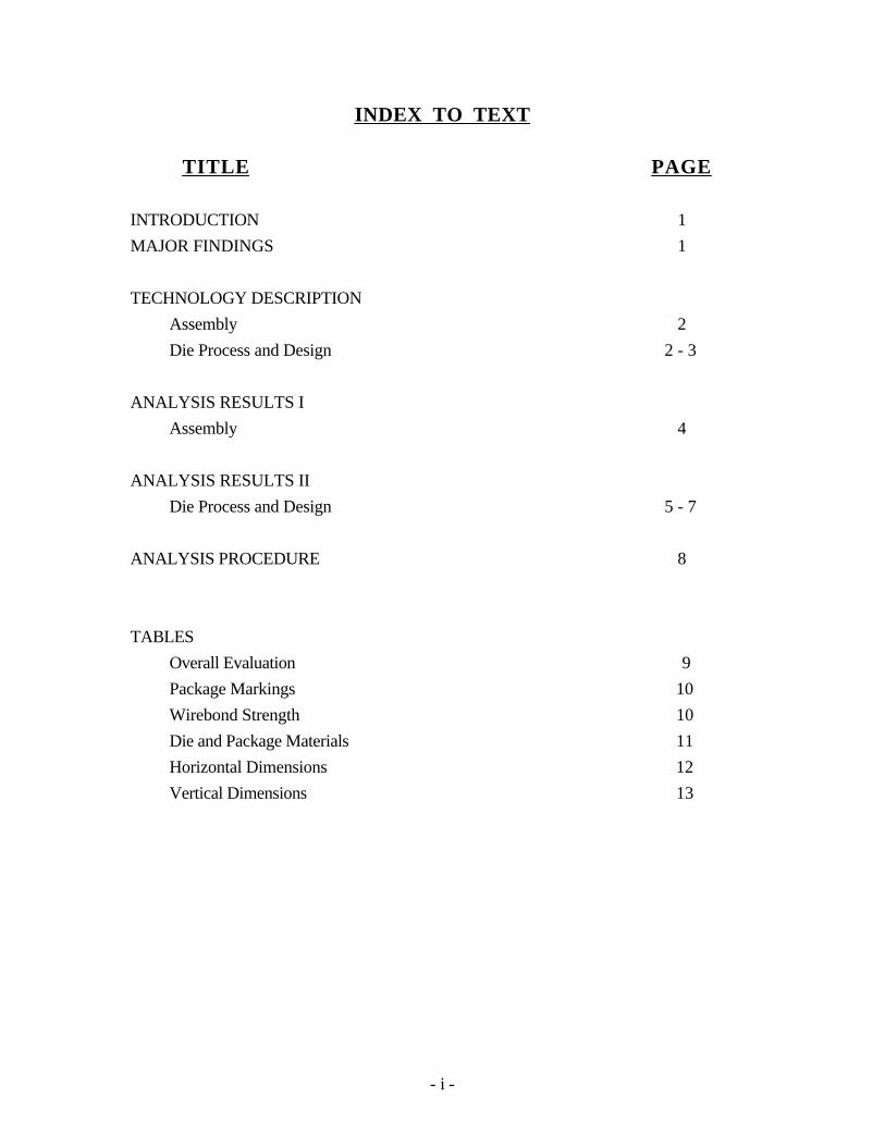
INDEX TO TEXT
TITLE PAGE
INTRODUCTION 1
MAJOR FINDINGS 1
TECHNOLOGY DESCRIPTION
Assembly 2
Die Process and Design 2 - 3
ANALYSIS RESULTS I
Assembly 4
ANALYSIS RESULTS II
Die Process and Design 5 - 7
ANALYSIS PROCEDURE 8
TABLES
Overall Evaluation 9
Package Markings 10
Wirebond Strength 10
Die and Package Materials 11
Horizontal Dimensions 12
Vertical Dimensions 13

- 1 -
INTRODUCTION
This report describes a construction analysis of the QLogic ISP1040B SCSI I/O Processor.
Six devices were supplied for the analysis which were packaged in 208-pin Plastic Quad
Flat Packs (PQFPs) and date coded 9721.
MAJOR FINDINGS
Questionable Items:1 None.
Special Features:
• Three metal, twin-well CMOS process.
• Sub-micron gate lengths (0.5 micron).
1These items present possible quality or reliability concerns. They should be discussedwith the manufacturer to determine their possible impact on the intended application.

- 2 -
TECHNOLOGY DESCRIPTION
Assembly:
• Devices were packaged in 208-pin Plastic Quad Flat Packs (PQFPs).
• Copper (Cu) gull-wing leadframe tinned with tin-lead (SnPb) solder.
• Dimpled paddle for added package strength, paddle was seated on a heat-spreader
(Al). Paddle was attached to the heatspreader by a thermal adhesion. Heatspreader
was not visible on x-ray (Figure 2).
• Paddle was constructed of copper (Cu) and internally plated with silver (Ag).
• Lead-locking provisions (anchors) at all pins. Lead-locking holes at paddle tie bars.
• Thermosonic ball bond method employing 1.1 mil O.D. gold wire.
• Sawn dicing (full depth).
• Silver-epoxy die attach.
Die Process
• Fabrication process: Selective oxidation CMOS process employing twin-wells, on a P-
substrate.
• Overlay passivation: A layer of silicon-nitride over a multilayered glass over a thin
layer of silicon dioxide.
• Metallization: Three levels of metal defined by dry-etch techniques. All levels
consisted of aluminum with titanium-nitride caps and barriers and thin titanium
adhesion layers. All metal levels utilized standard vias and contacts.

- 3 -
TECHNOLOGY DESCRIPTION (continued)
• Intermetal dielectrics (IMD2 and IMD1): Both interlevel dielectrics consisted of
multiple layers of deposited glass with an SOG (spin on glass) between for
planarization.
• Pre-metal glass: A single layer of CVD glass (BPSG) over various densified oxides.
Reflow was done prior to contact cuts.
• Polysilicon: A single layer of dry-etched polycide (poly and tungsten-silicide). This
layer was used to form all gates on the die.
• Diffusions: Standard implanted N+ and P+ diffusions formed the sources/drains of
transistors. Oxide sidewall spacers were used to provide the LDD spacing and were
left in place.
• Isolation: LOCOS (local oxide). A step was noted in the oxide at well boundaries.
• Wells: Twin-wells were employed on a P substrate (no epi was used). The step in
the oxide indicates a twin-well process was employed.
• Memory cells: A 7T SRAM cell design consisting of three polycide select gates, two
polycide storage gates, and two polycide pull-up transistors. Metal 3 was not
directly used in the array. Metal 2 provided bit lines, word line B, and distributed
GND and Vcc. Metal 1 provided cell interconnect and word lines A and C.
Polycide formed all gates.
• Buried contacts: No buried (poly-to-diffusion) contacts were employed.
• No fuses were noted.
• Anti-dishing patterns were employed and power bus lines were slotted and beveled
for stress relief.

- 4 -
ANALYSIS RESULTS I
Assembly: Figures 1 - 8
Questionable Items:1 None.
Special Features:
• Dimpled paddle on heatspreader.
General Items:
• Devices were packaged in 208-pin Plastic Quad Flat Packs (PQFPs).
• Overall package quality: Normal. No defects were found on the external or internal
portions of the packages. The leadframe was constructed of copper (Cu) and tinned
with tin-lead (SnPb). External pins were well formed and tinning of the leads was
complete. No gaps were noted at lead exits. The paddle was plated with silver.
Dimpled paddles were used for added package strength. The heatspreader (Al) was
used below the paddle to distribute heat evenly in the package.
• Wirebonding: Thermosonic ball bond method using 1.1 mil O.D. gold wire. No
bond lifts occurred and bond pull strengths were good (see page 10). Wire spacing
and placement was also good; intermetallic formation was complete. All three metal
levels formed the bond pad structure.
• Die attach: Silver-epoxy of normal quantity and quality.
• Die dicing: Die separation was by sawing (full depth) and showed normal quality
workmanship. No large chips or cracks were present at the die surface.
1These items present possible quality or reliability concerns. They should be discussed with the manufacturer to determine their possible impact on the intended application.

- 5 -
ANALYSIS RESULTS II
Die Process and Design: Figures 9 - 30
Questionable Items:1 None.
Special Features:
• Three metal, twin-well, CMOS process.
• Sub-micron gate lengths (0.5 micron P-channel).
General Items:
• Fabrication process: Selective oxidation CMOS process employing twin-wells in a P
substrate (no epi).
• Design and layout: Die layout was clean and efficient. Alignment was good at all
levels.
• Die surface defects: None. No contamination, toolmarks, or processing defects
were noted.
• Overlay passivation: A layer of silicon-nitride over a multilayered glass over a layer
of silicon-dioxide. Overlay integrity tests indicated defect-free passivation. Edge
seal was good.
• Metallization: Three levels of metal defined by dry-etch techniques. All levels
consisted of aluminum with titanium-nitride caps and barriers and thin titanium
adhesion layers. All metal levels utilized standard vias and contacts.
1These items present possible quality or reliability concerns. They should be discussed with the manufacturer to determine their possible impact on the intended application.

- 6 -
ANALYSIS RESULTS II (continued)
• Metal patterning: All metal layers were defined by a dry etch of good quality.
Contacts and vias were completely surrounded by aluminum. Metal 1 and 2 lines
were widened around contacts.
• Metal defects: None. No voiding or notching of the metal layers was found. No
silicon nodules were observed following removal of the metal layers.
• Metal step coverage: Metal 3 aluminum thinning up to 25 percent. Metal 2
aluminum thinning up to 65 percent thinning. Metal 3 aluminum thinning up to 60
percent. No problems foreseen.
• Intermetal dielectrics (IMD2 and IMD1): Both interlevel dielectrics consisted of
multiple layers of deposited glass with an SOG (spin on glass) between for
planarization.
• Contacts: Via and contact cuts appeared to be defined by a dry-etch process. No
significant over-etching was found. The cap metals were cleared on metals 1 and 2
at vias for better adhesion. Contact cuts were sloped at all levels to aid in metal
coverage.
• Pre-metal glass: A single layer of CVD glass (BPSG) over various densified oxides.
Reflow was done prior to contact cuts.
• Polysilicon: A single layer of dry-etched polycide (poly and tungsten-silicide). This
layer was used to form all gates on the die. Definition and coverage was good.
• Isolation: Local oxide (LOCOS). No problems were present at the birdsbeaks or
elsewhere.
• Diffusions: Standard implanted N+ and P+ diffusions formed the sources/drains of
transistors. An LDD process was used employing oxide sidewall spacers. The
spacers were left in place. Diffusions were not silicided. No problems were found
in these areas.

- 7 -
ANALYSIS RESULTS II (continued)
• Wells: Twin-wells in a P substrate. Definition was normal. The P-well could not
be delineated; however the step in the oxide at the well boundaries indicates a twin-
well process was employed.
• Buried contacts: No buried contacts were used.
Special Items:
• ESD sensitivity: Two samples were subjected to ESD tests which revealed all pins
passed following pulses of + 4000V.

- 8 -
PROCEDURE
The devices were subjected to the following analysis procedures:
External inspection
ESD sensitivity test
X-ray
Package section and material analysis
Decapsulation
Internal optical inspection
SEM inspection of assembly features and passivation
Passivation integrity test
Wirepull test
Passivation removal and inspect metal 3
Delayer to metal 2 and inspect
Delayer to metal 1 and inspect
Delayer to poly and inspect poly structures and die surface
Die sectioning (90° for SEM)*
Measure horizontal dimensions
Measure vertical dimensions
Die material analysis
WDX analysis
*Delineation of cross-sections is by silicon etch unless otherwise indicated.

- 9 -
OVERALL QUALITY EVALUATION: Overall Rating: Normal
DETAIL OF EVALUATION
Package integrity G
Package markings G
Die placement N
Die attach quality N
Wire spacing N
Wirebond placement G
Wirebond quality G
Dicing quality G
Wirebond method Thermosonic ball bonds using 1.1 mil
gold wire.
Die attach method Silver-epoxy
Dicing method Sawn (full depth)
Die surface integrity:
Toolmarks (absence) N
Particles (absence) N
Contamination (absence) G
Process defects (absence) G
General workmanship N
Passivation integrity G
Metal definition N
Metal integrity N
Contact coverage G
Contact registration G
Contact defects G
G = Good, P = Poor, N = Normal, NP = Normal/Poor

- 10 -
PACKAGE MARKINGS
Top Bottom
QLogic TM Corp. (Molded Markings)ISP1040B 2405101 KOREA (plus numbers)MCL7D23/N9721DUSPAT#5,276,807
WIREBOND STRENGTH
Wire material: 1.1 mil diameter gold
Die pad material: aluminum
Material at package post: silver
Sample # 1
# of wires tested: 30
Bond lifts: 0
Force to break - high: 15 g
- low: 10 g
- avg.: 12.2 g
- std. dev.: 1.7

- 11 -
DIE MATERIAL ANALYSIS
Passivation: A layer of silicon-nitride over a multilayeredglass over a layer of silicon-dioxide.
Metal 3: Aluminum titanium-nitride cap and barrier. Athin titanium adhesion layer under the barrier.
Intermetal dielectrics (IMD2 and IMD1): Multiple layers of silicon-dioxide with anSOG between.
Metal 2: Aluminum with a nitride cap and barrier. Athin titanium adhesion layer under the barrier.
Metal 1: Aluminum with a nitride cap and barrier. Athin titanium adhesion layer under the barrier.
Pre-metal glass: A borophosphosilicate glass (BPSG) containing 7.6wt. percent phosphorous and 3.3 wt. percentboron, over a layer of densified oxide.
Polycide: Tungsten-silicide on polysilicon.
PACKAGE MATERIAL ANALYSIS
Leadframe: Copper (Cu)
Internal plating: Silver (Ag)
External plating: Tin-solder (SnPb)
Die attach: Silver-epoxy (Ag)

- 12 -
HORIZONTAL DIMENSIONS
Die size: 9.1 x 8.2 mm (358 x 322 mils)
Die area: 74.5 mm2 (115, 276 mils2)
Min pad size: 0.06 x 0.06 mm (4 x 4 mils)
Min pad window: 0.05 x 0.05 mm (3.5 x 3.5 mils)
Min pad space: 20 microns
Min metal 3 width: 1.5 micron
Min metal 3 space: 1.2 micron
Min metal 3 pitch: 2.7 microns
Min via (M3 - M2): 0.7 micron (round)
Min metal 2 width: 0.9 micron
Min metal 2 space: 1.5 micron
Min metal 2 pitch: 2.4 microns
Min via (M2 - M1): 0.8 micron (round)
Min metal 1 width: 1.0 micron
Min metal 1 space: 1.6 micron
Min metal 1 pitch: 2.6 microns
Min contact: 0.8 micron (round)
Min polycide width: 0.5 micron
Min polycide space: 0.7 micron
Min gate length - (N-channel): 0.6 micron
- (P-channel): 0.5 micron

- 13 -
VERTICAL DIMENSIONS
Die thickness: 0.4 mm (16.5 mils)
Layers
Passivation 3: 0.45 micron
Passivation 2: 0.35 micron
Passivation 1: 0.08 micron
Metallization 3 - cap: 0.02 micron (approximate)
- aluminum: 0.75 micron
- barrier: 0.04 micron
Intermetal dielectric 2 (IMD2) - glass 2: 0.45 micron
- glass 1: 0.2 micron
Metallization 2 - cap: 0.02 micron (approximate)
- aluminum: 0.55 micron
- barrier: 0.07 micron
Intermetal dielectric 1 (IMD1) - glass 3: 0.45 micron
- glass 2: 0.12 micron
- glass 1: 0.1 micron
Metallization 1 - cap: 0.03 micron (approximate)
- aluminum: 0.6 micron
- barrier: 0.1 micron
Pre-metal glass: 0.5 micron
Polycide - silicide: 0.15 micron
- poly: 0.1 micron
Local oxide: 0.4 micron
N+ diffusion: 0.2 micron
P+ diffusion: 0.25 micron
N-well: 4 microns (approximate)

- ii -
INDEX TO FIGURES
ASSEMBLY Figures 1 - 8
DIE LAYOUT AND IDENTIFICATION Figures 9 - 10
PHYSICAL DIE STRUCTURES Figures 11 - 27
COLOR DRAWING OF DIE STRUCTURE Figure 27a
CELL STRUCTURE Figures 28 - 30

Integrated Circuit Engineering CorporationQLogic ISP1040B
Figure 1. The QLogic ISP1040B package. Mag. 2.5x.

Integrated Circuit Engineering CorporationQLogic ISP1040B
Figure 2. The QLogic ISP1040B pinout.

Integrated Circuit Engineering CorporationQLogic ISP1040B
Figure 3. X-ray view of the package. Mag. 4x.

Figure 4. Optical view of the package illustrating general construction. Mag. 20x.
Integ
rated C
ircuit E
ng
ineerin
g C
orp
oratio
nQ
Lo
gic IS
P1040B
DIE
HEATSPREADER
PADDLEPLASTIC
PACKAGELEADFRAME

Mag. 800x
Mag. 80x
Figure 5. Optical views of lead forming and lead exit.
Integrated Circuit Engineering CorporationQLogic ISP1040B
LEADFRAME
Cu LEADFRAME
SnPb TINNING

Mag. 320x
Mag. 100x
Figure 6. Optical views of dicing and die attach.
Integrated Circuit Engineering CorporationQLogic ISP1040B
DIE
Cu PADDLE DIMPLES
DIE
Cu PADDLE
Ag EPOXY
Ag INTERNAL PLATING
HEATSPREADER Al

Mag. 280x
Mag. 140x
Figure 7. SEM views of die corner and edge seal. 60°.
Integrated Circuit Engineering CorporationQLogic ISP1040B
DIE ATTACHATTACKED DURINGDECAPSULATION
PADDLE
DIE
EDGE OFPASSIVATION

Mag. 6800x
Mag. 350x
Figure 7a. SEM section views of the bond pad and edge seal structure.
Integrated Circuit Engineering CorporationQLogic ISP1040B
Au
PASSIVATIONMETAL 3
METAL 2
METAL 1
PRE-METALGLASS
EDGE OF PASSIVATION
EDGE OF DIE

Mag. 600x, 60°
Mag. 800x
Mag. 925x, 60°
Integrated Circuit Engineering CorporationQLogic ISP1040B
Figure 8. Optical and SEM views of typical wirebonds.
Au
Au
PAD
Au
LEADFRAME
DIE

Integrated Circuit Engineering CorporationQLogic ISP1040B
Figure 9. The QLogic ISP1040B intact circuit die. Mag. 18x.

Figure 9a. Optical view of markings from the surface of the die. Mag. 300x.
Integrated Circuit Engineering CorporationQLogic ISP1040B
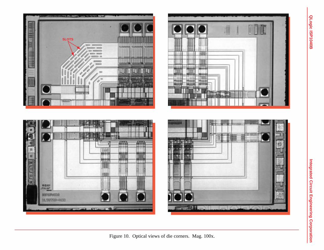
Figure 10. Optical views of die corners. Mag. 100x.
Integ
rated C
ircuit E
ng
ineerin
g C
orp
oratio
nQ
Lo
gic IS
P1040B
SLOTS

glass etch, Mag. 7700x
Mag. 6500x
Figure 11. SEM section views illustrating general construction.
Integrated Circuit Engineering CorporationQLogic ISP1040B
PASSIVATION 3
LOCAL OXIDE
POLY GATES
METAL 3METAL 2
METAL 1
S/D
PASSIVATION 2
PASSIVATION 3
POLY GATE
METAL 3METAL 2
METAL 1
IMD 1
IMD 2
PASSIVATION 2

Mag. 8800x
Mag. 4400x
Figure 11a. SEM views illustrating passivation coverage. 60°.
Integrated Circuit Engineering CorporationQLogic ISP1040B
ANTI-DISHING PATTERNS

Mag. 26,000x
Mag. 13,000x
Figure 12. SEM section views of metal 3 line profiles.
Integrated Circuit Engineering CorporationQLogic ISP1040B
PASSIVATION 3
PASSIVATION 2
PASSIVATION 1
METAL 3
IMD 2
IMD 2
IMD 1
METAL 2
PASSIVATION 3
PASSIVATION 2
METAL 3
PASSIVATION 1
BARRIER ADHESION LAYER

Mag. 5900x
Mag. 3700x
Figure 13. Topological SEM views of metal 3 patterning. 0°.
Integrated Circuit Engineering CorporationQLogic ISP1040B
VIA
METAL 3
METAL 3
METAL 2
Mag. 9100x
Mag. 20,000x
Mag. 20,000x
Integrated Circuit Engineering CorporationQLogic ISP1040B
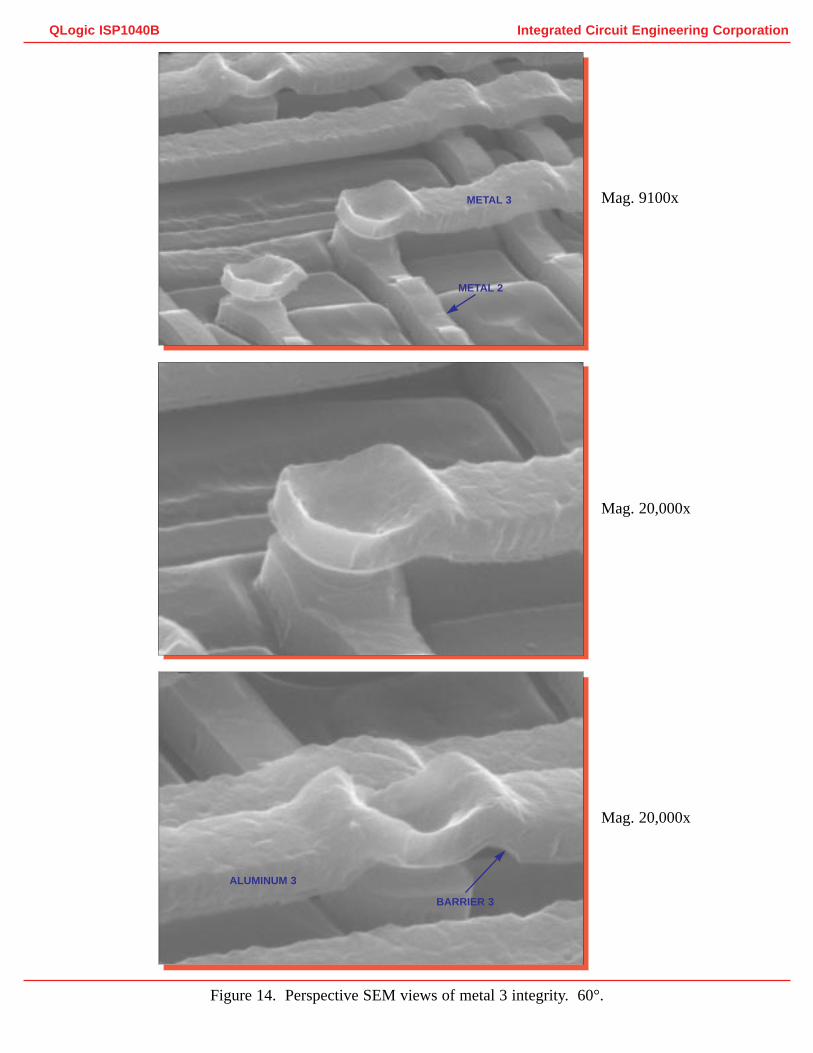
Figure 14. Perspective SEM views of metal 3 integrity. 60°.
METAL 3
METAL 2
ALUMINUM 3
BARRIER 3

Figure 15. SEM section view of metal 3-to-metal 2 via. Mag. 26,000x.
Integrated Circuit Engineering CorporationQLogic ISP1040B
PASSIVATION 3
PASSIVATION 2
PASSIVATION 1
METAL 3
METAL 2

Mag. 26,000x
Mag. 14,800x
Figure 16. SEM section views of metal 2 line profiles.
Integrated Circuit Engineering CorporationQLogic ISP1040B
IMD 2
METAL 2
IMD 1
PRE-METAL GLASS
CAP 2 SOG
ALUMINUM 2
BARRIER 2 ADHESION LAYER

Mag. 5000x
Mag. 2700x
Figure 17. Topological SEM views of metal 2 patterning. 0°.
Integrated Circuit Engineering CorporationQLogic ISP1040B
METAL 2

Figure 18. Perspective SEM views of metal 2 integrity. 60°.
Mag. 7700x
Mag. 29,600x
Integrated Circuit Engineering CorporationQLogic ISP1040B
Figure 18a. SEM section view of a metal 2-to-metal 1 via. Mag. 26,000x
CAP 2
IMD 1
CAP 1
ALUMINUM 2
65% THINNING
ALUMINUM 1
BARRIER 2
BARRIER 1
PRE-METAL GLASS
METAL 2
CAP 2
ALUMINUM 2
BARRIER 2

Mag. 52,000x
Mag. 26,000x
Figure 19. SEM section views of metal 1 line profiles.
Integrated Circuit Engineering CorporationQLogic ISP1040B
ALUMINUM 1
BARRIER 1
LOCOS
IMD 1SOG
ALUMINUM 1
BARRIER 1
ADHESION LAYER

Mag. 4200x
Mag. 4400x
Mag. 6200x
Integrated Circuit Engineering CorporationQLogic ISP1040B
Figure 20. Topological SEM views of metal 1 patterning. 0°.
METAL 1
METAL 1
METAL 1RESIDUAL GLASS

Mag. 32,200x
Mag. 6500x
Figure 21. Perspective SEM views of metal 1 integrity. 60°.
Integrated Circuit Engineering CorporationQLogic ISP1040B
METAL 1
CAP 1
ALUMINUM 1
BARRIER 1
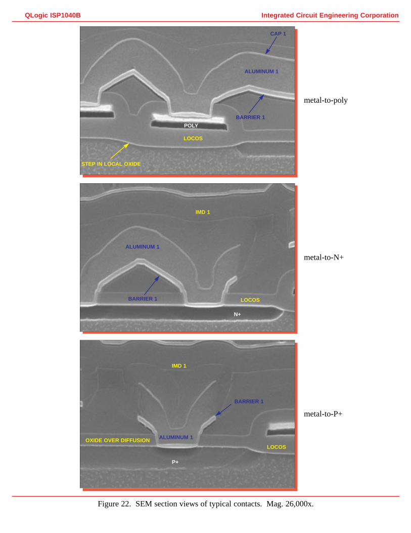
metal-to-poly
metal-to-N+
metal-to-P+
Integrated Circuit Engineering CorporationQLogic ISP1040B
Figure 22. SEM section views of typical contacts. Mag. 26,000x.
CAP 1
ALUMINUM 1
BARRIER 1
LOCOS
POLY
STEP IN LOCAL OXIDE
ALUMINUM 1
IMD 1
LOCOS
N+
IMD 1
LOCOSOXIDE OVER DIFFUSION ALUMINUM 1
BARRIER 1
P+
BARRIER 1

Mag. 6500x
Mag. 3100x
Figure 23. Topological SEM views of polycide patterning. 0°.
Integrated Circuit Engineering CorporationQLogic ISP1040B
POLY
DIFFUSION
POLY
N+
P+
GATES

Mag. 4000x
Mag. 8000x
Mag. 26,000x
Integrated Circuit Engineering CorporationQLogic ISP1040B
Figure 24. SEM views of polycide coverage. 60°.
POLY
POLY DIFFUSION
POLY
LOCOS
SILICIDEDIFFUSION

N-channel
P-channel
glass-etch
Integrated Circuit Engineering CorporationQLogic ISP1040B
Figure 25. SEM section views of typical transistors. Mag. 52,000x.
PRE-METAL GLASS
GATE OXIDE
SILICIDE
POLY
N+ S/D
SILICIDE
P+ S/D
SIDEWALL SPACER
SILICIDE
POLY
GATE OXIDE

Figure 26. Optical view of well structure. Mag. 1240x.
Integrated Circuit Engineering CorporationQLogic ISP1040B
Figure 27. SEM section views of a typical birdsbeak.
Mag. 13,000x
Mag. 52,000x
N-WELL
P-SUBSTRATE
METAL 3
METAL 1
LOCAL OXIDE
LOCAL OXIDE
POLYDENSIFIED OXIDE
GATE OXIDE

Figure 27a. Color cross section drawing illustrating device structure.
Orange = Nitride, Blue = Metal, Yellow = Oxide, Green = Poly,
Red = Diffusion, and Gray = Substrate
Integ
rated C
ircuit E
ng
ineerin
g C
orp
oratio
nQ
Lo
gic IS
P1040B
��������������������������������������
������������������������������
���������������������������P+ S/D
POLYSILICIDE
N+ S/D
N-WELLP-WELL
LOCAL OXIDE
����
��������
���������������������������
���������
���������
���������
����������
��������������
���������
������������
������������������������
����
PASSIVATION 3
PASSIVATION 2
PASSIVATION 1
ALUMINUM 3
ALUMINUM 2
ALUMINUM 1
CAP 3 SOG
BARRIER 3
CAP 2BARRIER 2
CAP 1 BARRIER 1
IMD 2
IMD 1
PRE-METAL GLASS
P-SUBSTRATE

metal 2
metal 1
delayered
Integrated Circuit Engineering CorporationQLogic ISP1040B
Figure 28. Perspective SEM views of the SRAM cell array. Mag. 4200x, 60°.
BITLINE
WORD LINES
RESIDUAL GLASS
WORD LINES

metal 1
metal 2
Figure 29. Topological SEM views of SRAM cell. Mag. 2400x, 0°.
Integrated Circuit Engineering CorporationQLogic ISP1040B
BIT
BIT
GND
VCC
WORD B
BITBIT
WORD C WORD A

Mag. 2400x, 0°
Figure 30. Topological SEM view and schematic of SRAM cell.
WORD C
WORD B
WORD A
BIT5 6
42
31
BIT 7
Integrated Circuit Engineering CorporationQLogic ISP1040B
1
2
3
45 6 7