qpf4006 product datasheet
TRANSCRIPT

QPF4006 37 – 40.5 GHz GaN Front End Module
Data Sheet Rev. L, Nov 2021 | Subject to change without notice - 1 of 23 - www.qorvo.com
Product Description The QPF4006 is a multi-function Gallium Nitride MMIC front-end module targeted for 39 GHz phased array 5G base stations and terminals. The device combines a low noise high linearity LNA, a low insertion-loss high-isolation TR switch, and a high-gain high-efficiency multi-stage PA. The QPF4006 operates from 37 GHz to 40.5 GHz range. The receive path (LNA+TR SW) is designed to provide 18dB of gain and a noise figure less than 4.5 dB. The transmit path (PA+SW) provides 23 dB of small signal gain and a saturated output power of 2 W.
The compact 4.5 mm x 4.0 mm surface mount package configuration is designed to meet the tight lattice spacing requirements for phased array applications. The QPF4006 is fabricated on Qorvo’s 0.15um GaN on
SiC process. It is housed in an air-cavity laminate package
with an embedded copper heat slug. The copper slug,
coupled with a low thermal resistance die-attach process,
allows the QPF4006 to operate at the extreme case
temperatures needed in phased array applications. Functional Block Diagram
Applications • 5G Wireless Base stations and terminals
• Point to Point Communications
Part No. Description QPF4006TR7 Tape and Reel, 7", Qty 250
QPF4006EVB03 QPF4006 Evaluation Board, Qty 1
Product Features • Frequency Range: 37 – 40.5 GHz
• RX Noise Figure: 4.2 dB
• RX Small Signal Gain: 18 dB
• RX Saturated Power: 17 dBm
• RX TOI : 20 dBm @ - 5 dBm Pin / tone
• TX Small Signal Gain: 23 dB
• TX Saturated Power: 33 dBm
• TX TOI: 42 dBm @ 24 dBm Pout / tone
• TX ACPR: 32dBc @ 24dBm average Pout 2
• TX Linearity: 4% EVM @ 24 dBm average Pout 2
• TX PAE: 7% @ 24 dBm average Pout. • Package Dimensions: 4.5 x 4.0 x 1.8 mm
1. Performance is typical at room temperature.
2. OFDM, 400 MHz modulation bandwidth, 64QAM.

QPF4006 37 – 40.5 GHz GaN Front End Module
Data Sheet Rev. L, Nov 2021 | Subject to change without notice - 2 of 23 - www.qorvo.com
Absolute Maximum Ratings
Parameter Value Drain Voltage (TXVD, RXVD) 28 V
Drain Current (TXID3+TXID12) 800 mA
Drain Current (RXID) 60 mA
Gate Voltage (RXVG, TXVG3, TXVG12) 0 to −5 V
Gate Current (RXIG, TXIG3, TXIG12) 20 mA
Switch Control Voltage (TXSW, RXSW) 0 to 28 V
Switch Control Current 20 mA
RF Input Power (All RF ports, 85 °C) 30 dBm
Channel Temperature, TCH 225 °C
Mounting Temperature (30 seconds) 260 °C
Storage Temperature −55 to 150 °C
Operation of this device outside the parameter ranges given above may cause permanent damage. These are stress ratings only, and functional operation of the device at these conditions is not implied. Extended application of Absolute Maximum Rating conditions to the device may reduce device reliability.
Normal Operating Conditions
Parameter Value
Drain Voltage 20 V
Drain Current (TXIDQ12 / TXIDQ3) 135 mA / 24 mA *
Drain Current (RX, IDQ) 15 mA
Gate Voltage (TXVG12/TXVG3) −2 V / -2.4 V
Gate Voltage (RXVG) -2 V
Control Voltage (TXSW, RXSW) TXSW = 0 V, RXSW = 20V (RX on, TX off) TXSW = 20 V, RXSW = 0V (RX off, TX on)
Operating Temperature Range −40 to 95 °C
Gate voltage shown are typical, can be adjusted to set required drain current. Electrical specifications are measured at specified test conditions. Specifications are not guaranteed over all recommended operating conditions.
* Other current settings: 45 / 60 mA = 105 mA; 90 / 120 mA = 210 mA; 135 / 180 mA = 315 mA (gate controls combined together).

QPF4006 37 – 40.5 GHz GaN Front End Module
Data Sheet Rev. L, Nov 2021 | Subject to change without notice - 3 of 23 - www.qorvo.com
Electrical Specifications RX
Test conditions, unless otherwise noted: VD = 20 V, IDQ = 15 mA. Data de-embedded to device reference planes, 25 °C
Parameter Min Typical Max Units
Frequency 37 40.5 GHz
Small Signal Gain (37 – 39 GHz) 12 18 dB
Small Signal Gain (40 – 40.5 GHz) 13 18 dB
Noise Figure 4.2 dB
Saturated Output Power 17 dBm
Input Return Loss 12 dB
Output Return Loss 15 dB
Output TOI, @ -5 dBm Pin / tone, 10 MHz tone spacing 20 dBm
Gain Temperature Coefficient −0.056 dB/°C
Electrical Specifications TX
Test conditions unless otherwise noted: VD = 20 V, TXIDQ12 / TXIDQ3 = 135mA / 24 mA Data de-embedded to device reference planes, 25 °C
Parameter Min Typical Max Units
Frequency 37 40.5 GHz
Small Signal Gain (37 GHz) 14 23 dB
Small Signal Gain (38 - 39 GHz) 12 23 dB
Small Signal Gain (40 - 40.5 GHz) 10 23 dB
Saturated Output Power 33 dBm
Input Return Loss 12 dB
Output Return Loss 13 dB
Output TOI, @ 24dBm Pout / tone, 10 MHz tone spacing 42 dBm
ACPR (24 dBm average power, OFDM, 400MHz, 64QAM) -32 dBc
EVM (24 dBm average power, OFDM, 400MHz, 64QAM) 4 %
PAE at average output power (24dBm) 7 %
Gain Temperature Coefficient −0.112 dB/°C

QPF4006 37 – 40.5 GHz GaN Front End Module
Data Sheet Rev. L, Nov 2021 | Subject to change without notice - 4 of 23 - www.qorvo.com
Performance Plots, Small Signal, Receive Path Test Conditions unless otherwise stated: RXVD = 20 V, RXIDQ = 15 mA, Data de-embedded to device reference planes, 25C
-30
-25
-20
-15
-10
-5
0
36 37 38 39 40 41
S11
(d
B)
Freq (GHz)
Input Return Loss vs Temp
- 40 C + 25 C + 85 C
10
12
14
16
18
20
22
24
36 37 38 39 40 41
Ga
in (
dB
)
Freq (GHz)
Gain vs Temp
- 40 C + 25 C + 85 C
-50
-45
-40
-35
-30
36 37 38 39 40 41
S1
2 (d
B)
Freq (GHz)
Reverse Isolation vs Temp
- 40 C + 25 C + 85 C
-30
-25
-20
-15
-10
-5
0
36 37 38 39 40 41
S2
2 (d
B)
Freq (GHz)
Output Return Loss vs Temp
- 40 C + 25 C + 85 C

QPF4006 37 – 40.5 GHz GaN Front End Module
Data Sheet Rev. L, Nov 2021 | Subject to change without notice - 5 of 23 - www.qorvo.com
Performance Plots, Small Signal, Receive Path Test Conditions unless otherwise stated: RXVD = 20 V, RXIDQ = 15 mA, Data de-embedded to device reference planes, 25 C
10
12
14
16
18
20
22
24
36 37 38 39 40 41
Ga
in (
dB
)
Freq (GHz)
Gain vs Voltage
18 V 20 V 22 V
10
12
14
16
18
20
22
24
36 37 38 39 40 41
Ga
in (
dB
)
Freq (GHz)
Gain vs Current
10 mA 15 mA
-30
-25
-20
-15
-10
-5
0
36 37 38 39 40 41
S11
(d
B)
Freq (GHz)
Input Return Loss vs Voltage
18 V 20 V 22 V
-30
-25
-20
-15
-10
-5
0
36 37 38 39 40 41
S11
(d
B)
Freq (GHz)
Input Return Loss vs Current
10 mA 15 mA
-30
-25
-20
-15
-10
-5
0
36 37 38 39 40 41
S2
2 (d
B)
Freq (GHz)
Output Return Loss vs Voltage
18 V 20 V 22 V
-30
-25
-20
-15
-10
-5
0
36 37 38 39 40 41
S2
2 (d
B)
Freq (GHz)
Output Return Loss vs Current
10 mA 15 mA
QPF4006 37 – 40.5 GHz GaN Front End Module
Data Sheet Rev. L, Nov 2021 | Subject to change without notice - 6 of 23 - www.qorvo.com
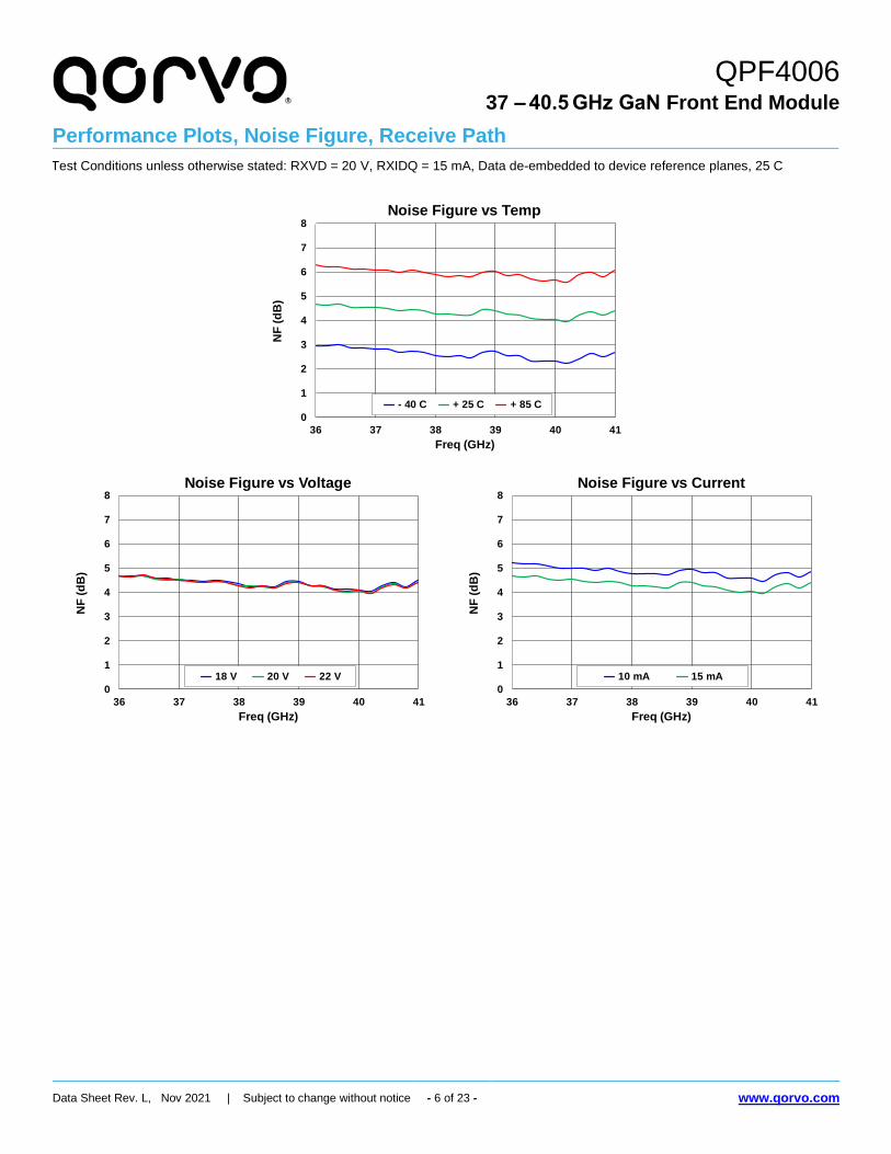
Performance Plots, Noise Figure, Receive Path Test Conditions unless otherwise stated: RXVD = 20 V, RXIDQ = 15 mA, Data de-embedded to device reference planes, 25 C
0
1
2
3
4
5
6
7
8
36 37 38 39 40 41
NF
(d
B)
Freq (GHz)
Noise Figure vs Temp
- 40 C + 25 C + 85 C
0
1
2
3
4
5
6
7
8
36 37 38 39 40 41
NF
(d
B)
Freq (GHz)
Noise Figure vs Voltage
18 V 20 V 22 V
0
1
2
3
4
5
6
7
8
36 37 38 39 40 41
NF
(d
B)
Freq (GHz)
Noise Figure vs Current
10 mA 15 mA
QPF4006 37 – 40.5 GHz GaN Front End Module
Data Sheet Rev. L, Nov 2021 | Subject to change without notice - 7 of 23 - www.qorvo.com
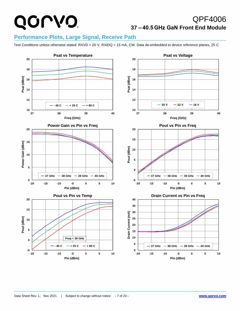
Performance Plots, Large Signal, Receive Path Test Conditions unless otherwise stated: RXVD = 20 V, RXIDQ = 15 mA, CW. Data de-embedded to device reference planes, 25 C
10
12
14
16
18
20
37 38 39 40
Ps
at
(dB
m)
Freq (GHz)
Psat vs Temperature
- 40 C + 25 C + 85 C
10
12
14
16
18
20
37 38 39 40
Ps
at
(dB
m)
Freq (GHz)
Psat vs Voltage
20 V 22 V 18 V
0
5
10
15
20
-20 -15 -10 -5 0 5 10
Po
we
r G
ain
(d
Bm
)
Pin (dBm)
Power Gain vs Pin vs Freq
37 GHz 38 GHz 39 GHz 40 GHz
-5
0
5
10
15
20
-20 -15 -10 -5 0 5 10
Po
ut
(dB
m)
Pin (dBm)
Pout vs Pin vs Freq
37 GHz 38 GHz 39 GHz 40 GHz
-5
0
5
10
15
20
-20 -15 -10 -5 0 5 10
Po
ut
(dB
m)
Pin (dBm)
Pout vs Pin vs Temp
- 40 C + 25 C + 85 C
Freq = 39 GHz
0
5
10
15
20
25
30
35
40
-20 -15 -10 -5 0 5 10
Dra
in C
urr
en
t (m
A)
Pin (dBm)
Drain Current vs Pin vs Freq
37 GHz 38 GHz 39 GHz 40 GHz

QPF4006 37 – 40.5 GHz GaN Front End Module
Data Sheet Rev. L, Nov 2021 | Subject to change without notice - 8 of 23 - www.qorvo.com
Performance Plots, Linearity, Receive Path Test Conditions unless otherwise stated: RXVD = 20 V, RXIDQ = 15 mA, Tone spacing: 10 MHz Data de-embedded to device reference planes, 25 C
15
16
17
18
19
20
21
22
23
24
25
37 38 39 40
OT
OI (d
Bm
)
Freq (GHz)
RX OTOI vs Freq vs Temp
- 40 C + 25 C + 85 C
Pin = -5 dBm / tone
15
16
17
18
19
20
21
22
23
24
25
37 38 39 40
OT
OI (d
Bm
)Freq (GHz)
RX OTOI vs Freq vs Voltage
18 V 20 V 22 V
Pin = -5 dBm / tone
-60
-50
-40
-30
-20
-10
0
-8 -6 -4 -2 0 2 4 6 8 10 12 14
IMD
3 (
dB
c)
Pout (dBm)
RX IMD3 vs Pout vs Freq
37 GHz 38 GHz 39 GHz 40 GHz
-80
-70
-60
-50
-40
-30
-20
-10
0
-8 -6 -4 -2 0 2 4 6 8 10 12 14
IMD
5 (
dB
c)
Pout (dBm)
RX IMD5 vs Pout vs Freq
37 GHz 38 GHz 39 GHz 40 GHz
QPF4006 37 – 40.5 GHz GaN Front End Module
Data Sheet Rev. L, Nov 2021 | Subject to change without notice - 9 of 23 - www.qorvo.com
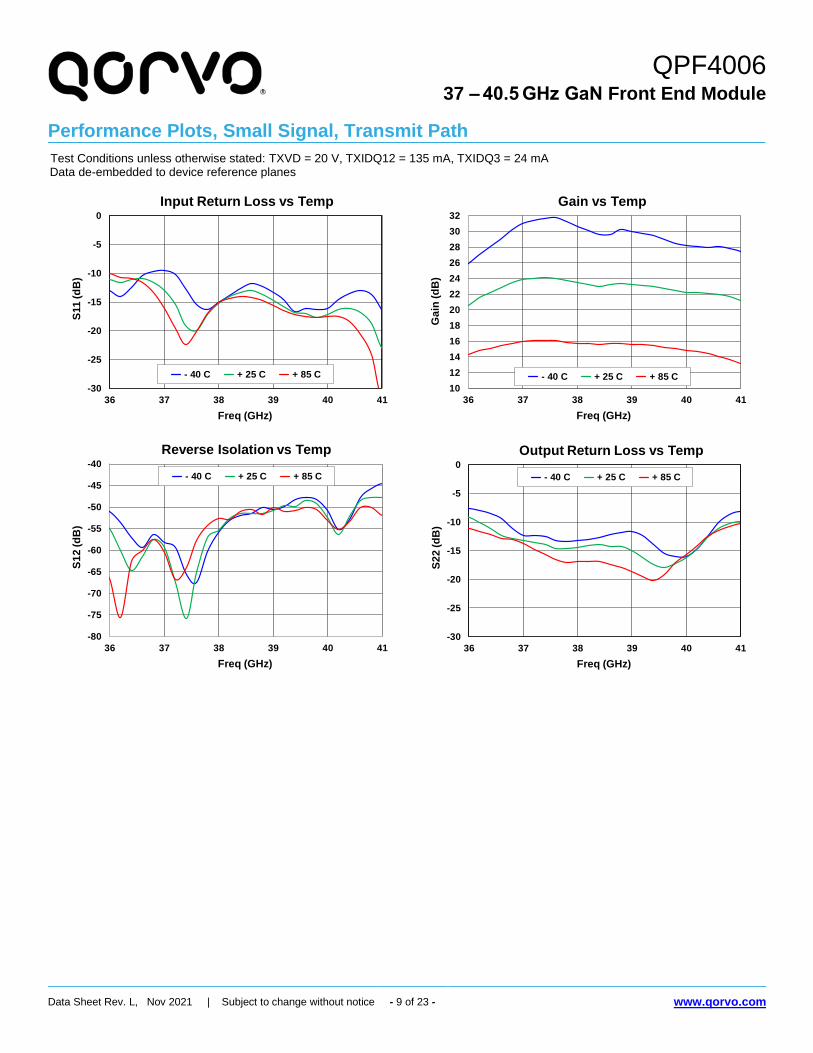
Performance Plots, Small Signal, Transmit Path Test Conditions unless otherwise stated: TXVD = 20 V, TXIDQ12 = 135 mA, TXIDQ3 = 24 mA Data de-embedded to device reference planes
-30
-25
-20
-15
-10
-5
0
36 37 38 39 40 41
S11
(d
B)
Freq (GHz)
Input Return Loss vs Temp
- 40 C + 25 C + 85 C
10
12
14
16
18
20
22
24
26
28
30
32
36 37 38 39 40 41
Ga
in (
dB
)
Freq (GHz)
Gain vs Temp
- 40 C + 25 C + 85 C
-80
-75
-70
-65
-60
-55
-50
-45
-40
36 37 38 39 40 41
S1
2 (d
B)
Freq (GHz)
Reverse Isolation vs Temp
- 40 C + 25 C + 85 C
-30
-25
-20
-15
-10
-5
0
36 37 38 39 40 41
S2
2 (d
B)
Freq (GHz)
Output Return Loss vs Temp
- 40 C + 25 C + 85 C

QPF4006 37 – 40.5 GHz GaN Front End Module
Data Sheet Rev. L, Nov 2021 | Subject to change without notice - 10 of 23 - www.qorvo.com
Performance Plots, Small Signal, Transmit Path Test Conditions unless otherwise stated: TXVD = 20 V, TXIDQ12 = 135 mA, TXIDQ3 = 24 mA Data de-embedded to device reference planes, 25 C
10
12
14
16
18
20
22
24
26
28
30
32
36 37 38 39 40 41
Ga
in (
dB
)
Freq (GHz)
Gain vs Voltage
+ 18 V + 20 V + 22 V
10
12
14
16
18
20
22
24
26
28
30
32
36 37 38 39 40 41
Ga
in (
dB
)
Freq (GHz)
Gain vs Current
105 mA 159 mA 210 mA
-30
-25
-20
-15
-10
-5
0
36 37 38 39 40 41
S11
(d
B)
Freq (GHz)
Input Return Loss vs Voltage
+ 18 V + 20 V + 22 V
-30
-25
-20
-15
-10
-5
0
36 37 38 39 40 41
S11
(d
B)
Freq (GHz)
Input Return Loss vs Current
105 mA 159 mA 210 mA
-30
-25
-20
-15
-10
-5
0
36 37 38 39 40 41
S2
2 (d
B)
Freq (GHz)
Output Return Loss vs Voltage
+ 18 V + 20 V + 22 V
-30
-25
-20
-15
-10
-5
0
36 37 38 39 40 41
S2
2 (d
B)
Freq (GHz)
Output Return Loss vs Current
105 mA 159 mA 210 mA

QPF4006 37 – 40.5 GHz GaN Front End Module
Data Sheet Rev. L, Nov 2021 | Subject to change without notice - 11 of 23 - www.qorvo.com
Performance Plots, Large Signal, Transmit Path Test Conditions unless otherwise stated: TXVD = 20 V, TXIDQ12 = 135 mA, TXIDQ3 = 24 mA, Pulse Mode: PW = 100 uS, DC = 10% Data de-embedded to device reference planes, 25 C
25
27
29
31
33
35
37
36 37 38 39 40 41
Ps
at
(dB
m)
Freq (GHz)
Psat vs Temperature
- 40 C + 25 C + 85 C
25
27
29
31
33
35
37
36 37 38 39 40 41
Ps
at
(dB
m)
Freq (GHz)
Psat vs Voltage
18 V 20 V 22 V
25
27
29
31
33
35
37
36 37 38 39 40 41
Ps
at
(dB
m)
Freq (GHz)
Psat vs Current
105 mA 159 mA 210 mA 315 mA

QPF4006 37 – 40.5 GHz GaN Front End Module
Data Sheet Rev. L, Nov 2021 | Subject to change without notice - 12 of 23 - www.qorvo.com
Performance Plots, Large Signal, Transmit Path Test Conditions unless otherwise stated: TXVD = 20 V, TXIDQ12 = 135 mA, TXIDQ3 = 24 mA, Pulse Mode: PW = 100 uS, DC = 10% Data de-embedded to device reference planes. 25C
-5
0
5
10
15
20
25
30
35
40
-10 -5 0 5 10 15 20
Po
ut
(dB
m)
Pin (dBm)
Pout vs Pin vs Temp
- 40 C + 25 C + 85 C
Freq = 39 GHz
-5
0
5
10
15
20
25
30
35
40
-10 -5 0 5 10 15 20
Po
ut
(dB
m)
Pin (dBm)
Pout vs Pin vs Freq
37 GHz 38 GHz 39 GHz 40 GHz
0
5
10
15
20
25
30
-10 -5 0 5 10 15 20
Po
we
r G
ain
(d
Bm
)
Pin (dBm)
Power Gain vs Pin vs Freq
37 GHz 38 GHz 39 GHz 40 GHz
0
100
200
300
400
500
600
700
800
-10 -5 0 5 10 15 20
Dra
in C
urr
en
t (m
A)
Pin (dBm)
Drain Current vs Pin vs Freq
37 GHz 38 GHz 39 GHz 40 GHz
0
5
10
15
20
25
-10 -5 0 5 10 15 20
PA
E (
%)
Pin (dBm)
PAE vs Pin vs Freq
37 GHz 38 GHz 39 GHz 40 GHz
0
5
10
15
20
25
10 15 20 25 30 35
PA
E (
%)
Pout (dBm)
PAE vs Pout vs Freq
37 GHz 38 GHz 39 GHz 40 GHz

QPF4006 37 – 40.5 GHz GaN Front End Module
Data Sheet Rev. L, Nov 2021 | Subject to change without notice - 13 of 23 - www.qorvo.com
Performance Plots, Linearity, Transmit Path Test Conditions unless otherwise stated: TXVD = 20 V, TXIDQ12 = 135 mA, TXIDQ3 = 24 mA, Tone Spacing = 10 MHz Data de-embedded to device reference planes, 25 C
30
35
40
45
50
37 38 39 40
OT
OI (d
Bm
)
Freq (GHz)
OTOI vs Freq vs Temp
- 40 C + 25 C + 85 C
Pout = 24 dBm / tone
30
35
40
45
50
37 38 39 40
OT
OI (d
Bm
)
Freq (GHz)
OTOI vs Freq vs VD
18 V 20 V
Pout = 24 dBm / tone
-60
-50
-40
-30
-20
-10
0
14 16 18 20 22 24 26 28 30
IMD
3 (
dB
c)
Pout (dBm)
IMD3 vs Pout vs Freq
37 GHz 38 GHz 39 GHz 40 GHz
-80
-70
-60
-50
-40
-30
-20
-10
0
14 16 18 20 22 24 26 28 30
IMD
5 (
dB
c)
Pout (dBm)
IMD5 vs Pout vs Freq
37 GHz 38 GHz 39 GHz 40 GHz

QPF4006 37 – 40.5 GHz GaN Front End Module
Data Sheet Rev. L, Nov 2021 | Subject to change without notice - 14 of 23 - www.qorvo.com
Performance Plots, Modulated Signal, Transmit Path Test Conditions unless otherwise stated: TXVD = 20 V, TXIDQ12 = 135 mA, TXIDQ3 = 24 mA, Source: 400 MHz OFDM, 64 QAM Data de-embedded to device reference planes, 25 C
-45
-40
-35
-30
-25
-20
-15
0 5 10 15 20 25 30 35
AC
PR
Lo
w (
dB
c)
Pout (dBm)
ACPR Low vs Pout vs Temp
- 40 C + 25 C + 85 C
Freq = 39 GHz
-45
-40
-35
-30
-25
-20
-15
0 5 10 15 20 25 30 35
AC
PR
Hig
h (
dB
c)
Pout (dBm)
ACPR High vs Pout vs Temp
- 40 C + 25 C + 85 C
Freq = 39 GHz
-45
-40
-35
-30
-25
-20
-15
5 10 15 20 25 30 35
AC
PR
Lo
w (
dB
c)
Pout (dBm)
ACPR Low vs Pout vs Freq
37 GHz 39 GHz 38 GHz 40 GHz
-45
-40
-35
-30
-25
-20
-15
5 10 15 20 25 30 35
AC
PR
Hig
h (
dB
c)
Pout (dBm)
ACPR High vs Pout vs Freq
37 GHz 39 GHz 38 GHz 40 GHz
-45
-40
-35
-30
-25
-20
-15
0 5 10 15 20 25 30 35
AC
PR
Lo
w (
dB
c)
Pout (dBm)
ACPR Low vs Pout vs Current
105 mA 159 mA 210 mA 315 mA
Freq = 39 GHz
-45
-40
-35
-30
-25
-20
-15
0 5 10 15 20 25 30 35
AC
PR
Hig
h (
dB
c)
Pout (dBm)
ACPR High vs Pout vs Current
105 mA 159 mA 210 mA 315 mA
Freq = 39 GHz

QPF4006 37 – 40.5 GHz GaN Front End Module
Data Sheet Rev. L, Nov 2021 | Subject to change without notice - 15 of 23 - www.qorvo.com
Performance Plots, Modulated Signal, Transmit Path Test Conditions unless otherwise stated: TXVD = 20 V, TXIDQ12 = 135 mA, TXIDQ3 = 24 mA, Source: 400 MHz OFDM, 64 QAM Data de-embedded to device reference planes, 25 C
0
2
4
6
8
10
12
14
0 5 10 15 20 25 30 35
PA
R (
dB
)
Pout (dBm)
PAR vs Pout vs Temp
- 40 C + 25 C + 85 C
PAR above 0.01 % of Signal Level, Freq = 39 GHz
0
2
4
6
8
10
12
14
5 10 15 20 25 30 35
PA
R (
dB
)
Pout (dBm)
PAR vs Pout vs Freq
37 GHz 39 GHz 38 GHz 40 GHz
PAR above 0.01 % of Signal Level
0
1
2
3
4
5
6
7
8
9
10
0 2 4 6 8 10 12 14 16 18 20 22 24 26 28 30
EV
M (
%)
Pout (dBm)
EVM vs Pout vs Temp
- 40 C + 25 C + 85 C
Freq: 39 GHz
0
1
2
3
4
5
6
7
8
9
10
0 2 4 6 8 10 12 14 16 18 20 22 24 26 28 30
EV
M (
%)
Pout (dBm)
EVM vs Pout vs Frequency
37 GHz 38 GHz 39 GHz 40 GHz

QPF4006 37 – 40.5 GHz GaN Front End Module
Data Sheet Rev. L, Nov 2021 | Subject to change without notice - 16 of 23 - www.qorvo.com
Performance Plots, Modulated Signal, Transmit Path Test Conditions unless otherwise stated: TXVD = 20 V, TXIDQ12 = 135 mA, TXIDQ3 = 24 mA, Source: 400 MHz OFDM, 64 QAM Data de-embedded to device reference planes, 25 C
10
15
20
25
30
35
0 5 10 15 20 25 30 35
Po
we
r G
ain
(d
B)
Pout (dBm)
Power Gain vs Pout vs Temp
- 40 C + 25 C + 85 C
Freq = 39 GHz10
15
20
25
30
35
5 10 15 20 25 30 35
Po
we
r G
ain
(d
B)
Pout (dBm)
Power Gain vs Pout vs Freq
37 GHz 39 GHz 38 GHz 40 GHz
0
5
10
15
20
25
0 5 10 15 20 25 30 35
PA
E (
%)
Pout (dBm)
PAE vs Pout vs Temp
- 40 C + 25 C + 85 C
Freq = 39 GHz
0
5
10
15
20
25
5 10 15 20 25 30 35
PA
E (
%)
Pout (dBm)
PAE vs Pout vs Freq
37 GHz 39 GHz 38 GHz 40 GHz
Freq = 39 GHz
0
2
4
6
8
10
0 5 10 15 20 25 30 35
Pd
iss
(W
)
Pout (dBm)
Pdiss vs Pout vs Temp
- 40 C + 25 C + 85 C
Freq = 39 GHz
0
50
100
150
200
250
300
350
400
0 5 10 15 20 25 30 35
Cu
rre
nt
(mA
)
Pout (dBm)
Current vs Pout vs Temp
- 40 C + 25 C + 85 C
Freq = 39 GHz

QPF4006 37 – 40.5 GHz GaN Front End Module
Data Sheet Rev. L, Nov 2021 | Subject to change without notice - 17 of 23 - www.qorvo.com
Mechanical Drawings & Pad Descriptions
Dimensions in mm Part Marking:
QPF4006: Part Number YY = Part Assembly Year
WW = Part Assembly Week MXXX = Batch ID
Pin Number Label Description 1, 2, 4, 5, 13, 15, 17, slug GND GROUND
3 ANT Antenna, DC Grounded
14 RXOUT Receive output, DC Blocked
16 TXIN Transmit input, DC Grounded
18 RXVG Receive gate control
19 RXVD Receive Drain Voltage
20 TXVG12 Transmit stage 1 and 2 gate controls
21 TXVG3 Transmit stage 3 gate control
22 TXVD Transmit Drain Voltage
23 TXSW Transmit switch control
24 RXSW Receive switch control
6, 7, 8, 9, 10, 11, 12 N/C No internal connection

QPF4006 37 – 40.5 GHz GaN Front End Module
Data Sheet Rev. L, Nov 2021 | Subject to change without notice - 18 of 23 - www.qorvo.com
Evaluation Board and Assembly
RF Layer is 0.008” thick Rogers Corp. RO4003C (εr = 3.35). Metal layers are 0.5 oz. copper. The microstrip line at the connector interface is optimized for the Southwest Microwave end launch connector 1492-04A-5.
Ref. Des. Component Value Manuf. Remark
C2, C4, C6, C8, C10 SMT Cap. CAP, 0402 1000pF +/-10% 50V 0402 X7R ROHS Various Red
C1, C3, C5, C7, C9 SMT Cap. CAP, 1206 1.0uF +/-10% 50V X7R ROHS Various Grey
R2, R4, R6 - R10 SMT Res. RES, 0402 5.1 OHM, 5% 50V, ROHS Various Green
R1, R3, R5 SMT Res. RES, 0402 0 OHM, 5%, ROHS Various Pink

QPF4006 37 – 40.5 GHz GaN Front End Module
Data Sheet Rev. L, Nov 2021 | Subject to change without notice - 19 of 23 - www.qorvo.com
Application Circuit
Bias-up Procedure Bias-down Procedure
1. Set drain supply TXVD limit to 700 mA, RXVD limit to 50 mA, gate and control supply limit to 10 mA each.
1. Turn off RF signal
2. Set TXVG12, TXVG3, RXVG to −5 V 2. Set TXVG12, TXVG3 and RXVG to −5 V
3. Set TXSW = 20 V (or 0 V), RXSW = 0 V (or 20 V) 3. Set VD = 0 V
4. Set VD = +20 V 4. Turn off drain supply
5. For TX, adjust TXVG12 to get TXID12 current, then adjust TXVG3 to achieve required total drain current; For RX, adjust RXVG to achieve required drain current.
5. Turn off TXSW, RXSW
6. Turn off gate supply
6. Apply RF signal

QPF4006 37 – 40.5 GHz GaN Front End Module
Data Sheet Rev. L, Nov 2021 | Subject to change without notice - 20 of 23 - www.qorvo.com
Thermal and Reliability Information
Parameter Values Units Conditions
Thermal Resistance (θJC), Quiescent, TX (1,2,3) 14.9 °C/W TX on, RX off, CW, VD = +20 V, IDQ = 159 mA,
TBASE = 85 °C
RF off, PDISS =3.18 W Channel Temperature (TCH), Quiescent, TX 132.4 °C
Thermal Resistance (θJC), Under Drive, TX (1,2,3) 10.7 °C/W TX on, RX off, CW, VD = +20 V, TBASE = 85 °C,
Freq = 39 GHz, PIN = 10 dBm, POUT = 25 dBm,
ID_DRIVE = 0.25 A, PDISS = 4.69 W Channel Temperature (TCH), Under Drive, TX 135.2 °C
Thermal Resistance (θJC), Quiescent, RX (1,2,3) 67.0 °C/W RX on, TX off, CW, VD = +20 V, IDQ = 15 mA
TBASE = 85 °C
RF off, PDISS = 0.3 W Channel Temperature (TCH), Quiescent, RX 105.1 °C
Notes:
1. Thermal resistance is measured to package backside
2. Base or ambient temperature is 85 °C
3. Refer to the following document: GaN Device Channel Temperature, Thermal Resistance, and Reliability Estimates

QPF4006 37 – 40.5 GHz GaN Front End Module
Data Sheet Rev. L, Nov 2021 | Subject to change without notice - 21 of 23 - www.qorvo.com
Solderability 1. Compatible with the latest version of J-STD-020, Lead-free solder, 260 °C.
2. This package is non-hermetic, and therefore cannot be subjected to aqueous washing.
The use of no-clean solder to avoid washing is highly recommended.
Recommended Soldering Temperature Profile

QPF4006 37 – 40.5 GHz GaN Front End Module
Data Sheet Rev. L, Nov 2021 | Subject to change without notice - 22 of 23 - www.qorvo.com
Tape and Reel Information
Standard T/R size = 250 pieces on a 7" reel.
Material Cavity (mm)
Distance Between Centerline (mm)
Carrier Tape (mm)
Cover Carrier (mm)
Vendor Vendor P/N Length (A0)
Width (B0)
Depth (K0)
Pitch (P1)
Length direction (P2)
Width Direction (F)
Width (W)
Width (W)
Tek-Pak QFN0400X 0450C
4.25 4.75 2.1 8.0 2.00 5.50 12.0 9.20

QPF4006 37 – 40.5 GHz GaN Front End Module
Data Sheet Rev. L, Nov 2021 | Subject to change without notice - 23 of 23 - www.qorvo.com
Handling Precautions
Parameter Rating Standard
Caution! ESD-Sensitive Device
ESD – Human Body Model (HBM) 0B ESDA / JEDEC JS-001-2012
ESD – Charged Device Model (CDM) C3 ESDA / JEDEC JS-002-2014
MSL – Convection Reflow 260 °C 3 JEDEC standard IPC/JEDEC
J-STD-020
RoHS Compliance This product is compliant with the 2011/65/EU RoHS directive (Restrictions on the Use of Certain Hazardous Substances in Electrical and Electronic Equipment), as amended by Directive 2015/863/EU. This product also has the following attributes:
• Lead Free
• Antimony Free
• TBBP-A (C15H12Br402) Free
• PFOS Free
Contact Information For the latest specifications, additional product information, worldwide sales and distribution locations:
Tel: 1-844-890-8163
Web: www.qorvo.com
Email: [email protected]
Important Notice The information contained herein is believed to be reliable; however, Qorvo makes no warranties regarding the information contained herein and assumes no responsibility or liability whatsoever for the use of the information contained herein. All information contained herein is subject to change without notice. Customers should obtain and verify the latest relevant information before placing orders for Qorvo products. The information contained herein or any use of such information does not grant, explicitly or implicitly, to any party any patent rights, licenses, or any other intellectual property rights, whether with regard to such information itself or anything described by such information. THIS INFORMATION DOES NOT CONSTITUTE A WARRANTY WITH RESPECT TO THE PRODUCTS DESCRIBED HEREIN, AND QORVO HEREBY DISCLAIMS ANY AND ALL WARRANTIES WITH RESPECT TO SUCH PRODUCTS WHETHER EXPRESS OR IMPLIED BY LAW, COURSE OF DEALING, COURSE OF PERFORMANCE, USAGE OF TRADE OR OTHERWISE, INCLUDING THE IMPLIED WARRANTIES OF MERCHANTABILITY AND FITNESS FOR A PARTICULAR PURPOSE.
Without limiting the generality of the foregoing, Qorvo products are not warranted or authorized for use as critical components in medical, life-saving, or life-sustaining applications, or other applications where a failure would reasonably be expected to cause severe personal injury or death.
© 2021 Qorvo US, Inc. All rights reserved. This document is subject to copyright laws in various jurisdictions worldwide and may not be reproduced or distributed, in whole or in part, without the express written consent of Qorvo US, Inc.