quad supply and line monitor (rev. a) - digi-key sheets/texas...quad supply and line monitor...
TRANSCRIPT

1FEATURES DESCRIPTION
BLOCK DIAGRAM
Note: Pin numbers refer to J, N and DW packages.
UC1903UC2903UC3903
www.ti.com ........................................................................................................................................ SLUS233A–OCTOBER 1999–REVISED SEPTEMBER 2008
Quad Supply and Line Monitor
• Inputs for Monitoring up to Four Separate The UC1903 family of quad supply and line monitorSupply Voltage Levels integrated circuits will respond to under- and
over-voltage conditions on up to four continuously• Internal Inverter for Sensing a Negative Supplymonitored voltage levels. An internal op-amp inverterVoltageallows at least one of these levels to be negative. A• Line/Switch Sense Input for Early Power separate line/switcher sense input is available to
Source Failure Warning provide early warning of line or other power source• Programmable Under- and Over-Voltage Fault failures.
Thresholds with Proportional Hysteresis The fault window adjustment circuit on these devices• A Precision 2.5-V Reference provides easy programming of under- and
over-voltage thresholds. The thresholds, centered• General Purpose Op-Amp for Auxiliary Usearound a precision 2.5-V reference, have an input• Three High Current, >3 0mA, Open-Collector hysteresis that scales with the window width forOutputs Indicate Over-Voltage, Under-Voltage precise, glitch-free operation. A reference output pinand Power OK Conditions allows the sense input fault windows to be scaled
• 8-V to 40-V Supply Operation with 7-mA independently using simple resistive dividers.Stand-By Current The three open collector outputs on these devices
sink in excess of 30 mA of load current when active.The under- and over-voltage outputs respond afterseparate, user defined, delays to respective faultconditions. The third output is active during any faultcondition including under- and over-voltage,line/switcher faults, and input supply under-voltage.The off state of this output indicates a "power OK"situation.
1
Please be aware that an important notice concerning availability, standard warranty, and use in critical applications of TexasInstruments semiconductor products and disclaimers thereto appears at the end of this data sheet.
PRODUCTION DATA information is current as of publication date. Copyright © 1999–2008, Texas Instruments IncorporatedProducts conform to specifications per the terms of the TexasInstruments standard warranty. Production processing does notnecessarily include testing of all parameters.
DESCRIPTION (CONT.)
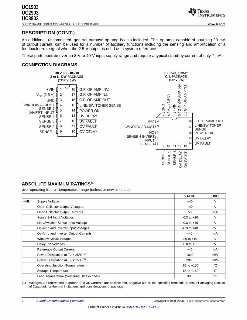
CONNECTION DIAGRAMS
1
2
3
4
5
6
7
8
9
18
17
16
15
14
13
12
11
10
+VIN
V (2.5 V)REF
GND
WINDOW ADJUSTSENSE 4
INVERT INPUTSENSE 4
G.P. OP-AMP INV.
LINE/SWITCHER SENSE
POWER OK
UV DELAY
UV FAULTSENSE 3
SENSE 2
SENSE 1
G.P. OP-AMP N.I.
G.P. OP-AMP OUT
OV FAULT
OV DELAY
DIL-18, SOIC-18J or N, DW PACKAGE
(TOP VIEW)
3 2 1 20 19
18
17
16
15
149 11 12 1310
4
5
6
7
8
+V
IN
WINDOW ADJUST
V(2
.5 V
)R
EF
GN
D
GND
NC
SENSE 4 INVERTINPUT
SENSE 4
SE
NS
E 3
SE
NS
E 2
SE
NS
E 1
OV
DE
LA
Y
OV
FA
ULT
UV FAULT
UV DELAY
LINE/SWITCHERSENSEPOWER OK
G.P. OP-AMP OUT
G.P
. O
P-A
MP
N.I.
G.P
. O
P-A
MP
INV
PLCC-20, LCC-20Q, L PACKAGE
(TOP VIEW)
ABSOLUTE MAXIMUM RATINGS (1)
UC1903UC2903UC3903SLUS233A–OCTOBER 1999–REVISED SEPTEMBER 2008 ........................................................................................................................................ www.ti.com
An additional, uncommitted, general purpose op-amp is also included. This op-amp, capable of sourcing 20 mAof output current, can be used for a number of auxiliary functions including the sensing and amplification of afeedback error signal when the 2.5-V output is used as a system reference.
These parts operate over an 8-V to 40-V input supply range and require a typical stand-by current of only 7 mA.
over operating free-air temperature range (unless otherwise noted)
VALUE UNIT+VIN Supply Voltage +40 V
Open Collector Output Voltages. +40 VOpen Collector Output Currents. 50 mASense 1-4 Input Voltages –0.3 to +20 VLine/Switcher Sense Input Voltage –0.3 to +40 VOp-Amp and Inverter Input Voltages –0.3 to +40 VOp-Amp and Inverter Output Currents . –40 mAWindow Adjust Voltage. 0.0 to +10 VDelay Pin Voltages 0.0 to +5 VReference Output Current –40 mAPower Dissipation at TA = 25°C (1) 1000 mWPower Dissipation at TC = 25°C (1) 2000 mWOperating Junction Temperature –55 to +150 °CStorage Temperature –65 to +150 CLead Temperature (Soldering, 10 Seconds) 300 °C
(1) Voltages are referenced to ground (Pin 3). Currents are positive into, negative out of, the specified terminals. Consult Packaging Sectionof Databook for thermal limitations and considerations of package.
2 Submit Documentation Feedback Copyright © 1999–2008, Texas Instruments Incorporated
Product Folder Link(s): UC1903 UC2903 UC3903

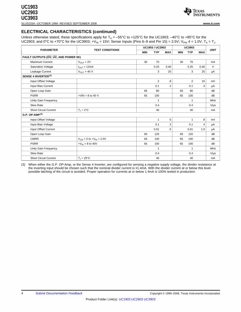
ELECTRICAL CHARACTERISTICS
UC1903UC2903UC3903
www.ti.com ........................................................................................................................................ SLUS233A–OCTOBER 1999–REVISED SEPTEMBER 2008
Unless otherwise stated, these specifications apply for TA = –55°C to +125°C for the UC1903; –40°C to +85°C for theUC2903; and 0°C to +70°C for the UC3903; +VIN = 15V; Sense Inputs (Pins 6–9 and Pin 15) = 2.5V; VPIN 4 = 1.0V, TA = TJ.
UC1903 / UC2903 UC3903PARAMETER TEST CONDITIONS UNIT
MIN TYP MAX MIN TYP MAX
SUPPLY
Input Supply Current No Faults 7 9 7 11 mA
UV, OV and Line Fault 10 15 10 18 mA
Supply Under Voltage Threshold Fault Outputs Enabled 6.0 7.0 7.5 5.5 7.0 8.0 V(VSUV)
Minimum Supply to Enable Power 3.0 4.0 3.0 4.0 VOK Output
REFERENCE
Output Voltage (VREF) TJ = 25°C 2.485 2.5 2.515 2.470 2.5 2.530 V
Over Temperature 2.465 2.535 2.465 2.535 V
Load Regulation IL = 0 to 10mA 1 10 1 15 mV
Line Regulation +VIN = 8 to 40V 1 4 1 8 mV
Short Circuit Current TJ = 25°C 40 40 mA
FAULT THRESHOLDS (1)
OV Threshold Adj. Offset from VREF as a function of VPIN 0.230 0.25 0.270 0.230 0.25 0.270 V/V4 Input = Low to High, 0.5V ≤ VPIN 4 ≤ 2.5V
UV Threshold Adj. Offset from VREF as a function of VPIN –0.270 –0.25 –0.230 –0.270 –0.25 –0.270 V/V4 Input = High to Low, 0.5V ≤ VPIN 4 ≤ 2.5V
OV & UV Threshold Hyst. 0.5V ≤ VPIN 4 ≤ 2.5V 10 20 30 10 20 30 mV/V
OV & UV Threshold Supply +VIN = 8V to 40V 0.002 0.01 0.002 0.02 %/VSensitivity
Adjust Pin (Pin 4) Input Bias Current 0.5V ≤ VPIN 4 ≤ 2.5V ±1 ±10 ±1 ±12 µA/V
Line Sense Threshold Input = High to Low 1.94 2.0 2.06 1.9 2.0 2.1 V
Line Sense Threshold Hyst. 125 175 225 100 175 250 mV
SENSE INPUTS
Input = 2.8V (2) 1 3 1 6 µASense 1-4 Input Bias Current
Input = 2.2 (2) –1 –3 –1 -6 µA
Line Sense Input Bias Current Input = 2.3V (2) 1 3 1 6 µA
OV AND UV FAULT DELAY
Charging Current 60 60 µA
Threshold Voltage Delay Pin = Low to High 1.8 1.8 V
Threshold Hysteresis TJ = 25°C 250 250 mV
Delay Ratio of Threshold Voltage to Charging 20 30 50 20 30 50 ms/µFCurrent
(1) Reference to pin numbers in this specification pertain to 18 pin DIL N and J packages and 18 pin SOIC DW package.(2) These currents represent maximum input bias currents required as the sense inputs cross appropriate thresholds.
Copyright © 1999–2008, Texas Instruments Incorporated Submit Documentation Feedback 3
Product Folder Link(s): UC1903 UC2903 UC3903
UC1903UC2903UC3903SLUS233A–OCTOBER 1999–REVISED SEPTEMBER 2008 ........................................................................................................................................ www.ti.com
ELECTRICAL CHARACTERISTICS (continued)Unless otherwise stated, these specifications apply for TA = –55°C to +125°C for the UC1903; –40°C to +85°C for theUC2903; and 0°C to +70°C for the UC3903; +VIN = 15V; Sense Inputs (Pins 6–9 and Pin 15) = 2.5V; VPIN 4 = 1.0V, TA = TJ.
UC1903 / UC2903 UC3903PARAMETER TEST CONDITIONS UNIT
MIN TYP MAX MIN TYP MAX
FAULT OUTPUTS (OV, UV, AND POWER 0K)
Maximum Current VOUT = 2V 30 70 30 70 mA
Saturation Voltage IOUT = 12mA 0.25 0.40 0.25 0.40 V
Leakage Current VOUT = 40 V 3 25 3 25 µA
SENSE 4 INVERTER (3)
Input Offset Voltage 2 8 2 10 mV
Input Bias Current 0.1 2 0.1 4 µA
Open Loop Gain 65 80 65 80 dB
PSRR +VIN = 8 to 40 V 65 100 65 100 dB
Unity Gain Frequency 1 1 MHz
Slew Rate 0.4 0.4 V/µs
Short Circuit Current TJ = 2°C 40 40 mA
G.P. OP-AMP (3)
Input Offset Voltage 1 5 1 8 mV
Input Bias Voltage 0.1 2 0.1 4 µA
Input Offset Current 0.01 .5 0.01 1.0 µA
Open Loop Gain 65 120 65 120 dB
CMRR VCM = 0 to +VIN = 2.0V 65 100 65 100 dB
PSRR +VIN = 8 to 40V 65 100 65 100 dB
Unity Gain Frequency 1 1 MHz
Slew Rate 0.4 0.4 V/µs
Short Circuit Current TJ = 25°C 40 40 mA
(3) When either the G.P. OP-Amp, or the Sense 4 Inverter, are configured for sensing a negative supply voltage, the divider resistance atthe inverting input should be chosen such that the nominal divider current is ≤1.4mA. With the divider current at or below this levelpossible latching of the circuit is avoided. Proper operation for currents at or below 1.4mA is 100% tested in production.
4 Submit Documentation Feedback Copyright © 1999–2008, Texas Instruments Incorporated
Product Folder Link(s): UC1903 UC2903 UC3903

UC1903
+VINREFERENCE
CIRCUIT
1.25 VQ2
Q1
Q3
R1
R2
R3
15 W
2.5 kW
2.5 kW
2.5 VOUTPUT
RA
RSVADJ BIASCANCELLATION
AND MIRRORCIRCUITS
I =O
VADJ
R4
R4
8 kW
R5
R6
R7
R8
1.84 kW
0.16 kW
0.16 kW
1.84 kW
IOC IOD Q5
Q4IOBIOA
TOOV HYSTERESISCONTROL
OV THRESHOLD
FAULT WINDOWTHREAHOLD and HYSTERESIS
CIRCUITS
UV THRESHOLD
TOUV HYSTERESISCONTROL
Typical Characteristics
0.2
0.1
0
- 0.1
- 0.2
- 0.3
- 0.4
- 0.5
- 0.6
- 0.7
- 55 - 35 - 15 5 25 45 65 85 105 125T - Junction Temperature - °CJ
Refe
ren
ce C
han
ge -
%
Typical 2.5 V Referencevs
Temperature Characteristic
40
Dela
y -
ms/
Fm
- 55 - 35 - 15 5 25 45 65 85 105 125T - Junction Temperature - °CJ
Typical Fault Delayvs
Temperature Characteristic (C 270 pF)DELAY ≥
35
30
25
20
UC1903UC2903UC3903
www.ti.com ........................................................................................................................................ SLUS233A–OCTOBER 1999–REVISED SEPTEMBER 2008
Block Diagram
A. The UC1903 fault window circuitry generates OV and UV thresholds centered around the 2.5-V reference. Windowmagnitude and threshold hysteresis are proportional to the window adjust input voltage at Pin 4.
Figure 1. Operation and Application Information
Copyright © 1999–2008, Texas Instruments Incorporated Submit Documentation Feedback 5
Product Folder Link(s): UC1903 UC2903 UC3903

OPERATION AND APPLICATION INFORMATION
Setting a Fault Window
ADJV2.5 V ±
4 (1)
( )S ADJV ± 10 × V % (2)
Hysteresis
FaultWindow
FaultWindow
No Fault
Fault
25
20
15
10
5
0
-5
-10
-15
-20
-25
Su
pp
ly F
au
lt W
ind
ow
- %
0 0.5 1 1.5 2 2.5
Window Adjust Voltage (V ) at Pin 4ADJ
3.125
3
2.875
2.750
2.625
2.5
2.25
2.125
2
2.375
1.875
Fa
ult
Win
do
w a
t S
en
se
In
pu
ts -
V
UC1903UC2903UC3903SLUS233A–OCTOBER 1999–REVISED SEPTEMBER 2008 ........................................................................................................................................ www.ti.com
The fault thresholds on the UC1903 are generated by creating positive and negative offsets, equal in magnitude,that are referenced to the chip’s 2.5-V reference. The resulting fault window is centered around 2.5 V and has amagnitude equal to that of the applied offsets. Simplified schematics of the fault window and reference circuitsare shown in Figure 1 along with the Typical Characteristics diagrams. The magnitude of the offsets isdetermined by the voltage applied at the window adjust pin, Pin 4. A bias cancellation circuit keeps the inputcurrent required at Pin 4 low, allowing the use of a simple resistive divider off the reference to set the adjust pinvoltage.
The adjust voltage at Pin 4 is internally applied across R4, and an 8-kΩ resistor. The resulting current is mirroredfour times to generate current sources IOA, IOB, IOC, and IOD, all equal in magnitude. When all four of the senseinputs are inside the fault window, a no-fault condition, Q4 and Q5 are turned on. In combination with D1 and D2this prevents LOB and LOD from affecting the fault thresholds. In this case, the OV and UV thresholds are equal toVREF + IOA(R5 + R6) and VREF – IOC(R7 + R8) respectively. The fault window can be expressed as:
In terms of a sensed nominal voltage level, VS, the window as a percent variation is:
When a sense input moves outside the fault window given in Equation 1, the appropriate hysteresis control signalturns off Q4 or Q5. For the under-voltage case, Q5 is disabled and current source IOB flows through D2. The netcurrent through R7 becomes zero as IOB cancels IOC, giving an 8% reduction in the UV threshold offset. Theovervoltage case is the same, with Q4 turning off, allowing IOD to cancel the current flow, IOA, through R6. Theresult is a hysteresis at the sense inputs which is always 8% of the window magnitude. This is shown graphicallyin Figure 2.
Figure 2. Fault Window and Threshold Hysteresis Scale as a Function of the Voltage Applied at Pin 4
6 Submit Documentation Feedback Copyright © 1999–2008, Texas Instruments Incorporated
Product Folder Link(s): UC1903 UC2903 UC3903

Fault Windows Scaled Independently
Fault window for the Sense Input,in percent, is:
–10 (VADJ) •R3 + R1R2/(R1 + R2)
R3,
for:
VS (NOM) •R2
R1 + R2= 2.5V
MonitoredSupply Voltage
VS
R1
R2R3
UC1903
SENSE 1-4 INPUT
2.5 VREF.
Fault window for the sense input, in percent, is:
•R2
R1 + R2
SENSEINPUT
R1
R2
UC1903
G.P. OP-AMP
2.5 VREF.
SENSE 1-4 INPUT
±10 (V )ADJ
UC1903UC2903UC3903
www.ti.com ........................................................................................................................................ SLUS233A–OCTOBER 1999–REVISED SEPTEMBER 2008
In many applications, it may be desirable to monitor various supply voltages, or voltage levels, with varying faultwindows. Using the reference output and external resistive dividers this is easily accomplished with the UC1903.Figure 3 and Figure 4 illustrate how the fault window at any sense input can be scaled independently of theremaining inputs.
A. Using the reference output and a resistive divider, a sense input with an independently wider fault window can begenerated.
Figure 3. UC1903 Sense Input with an Independently Wider Fault Window
A. The general purpose op-amp on the UC1903 can be used to create a sense input with an independently tighter faultwindow.
Figure 4. UC1903 Sense Input with an Independently Tighter Fault Window
Copyright © 1999–2008, Texas Instruments Incorporated Submit Documentation Feedback 7
Product Folder Link(s): UC1903 UC2903 UC3903
+VIN
75 Am
UC1903G.P. OP-AMP
OUTPUT STAGE
D1
TO OP-AMPINPUT STAGE
Q6
Q5Q4
Q1Q2
Q3
R1
10 kW
R2
15 W
R3
150 WOUTPUT
150 Am
R4
500 W
16
Sensing a Negative Voltage Level
Note: A similar scheme w/the G.P. op-amp will allow a sec-ond negative supply to be monitored.
2.5 V R1
R2VS
UC1903
SENSE 4 INPUT
SENSE 4INVERTER
GROUND
V (NOM) = 2.5 VSNEGATIVE
SUPPLY (-V )S
UC1903UC2903UC3903SLUS233A–OCTOBER 1999–REVISED SEPTEMBER 2008 ........................................................................................................................................ www.ti.com
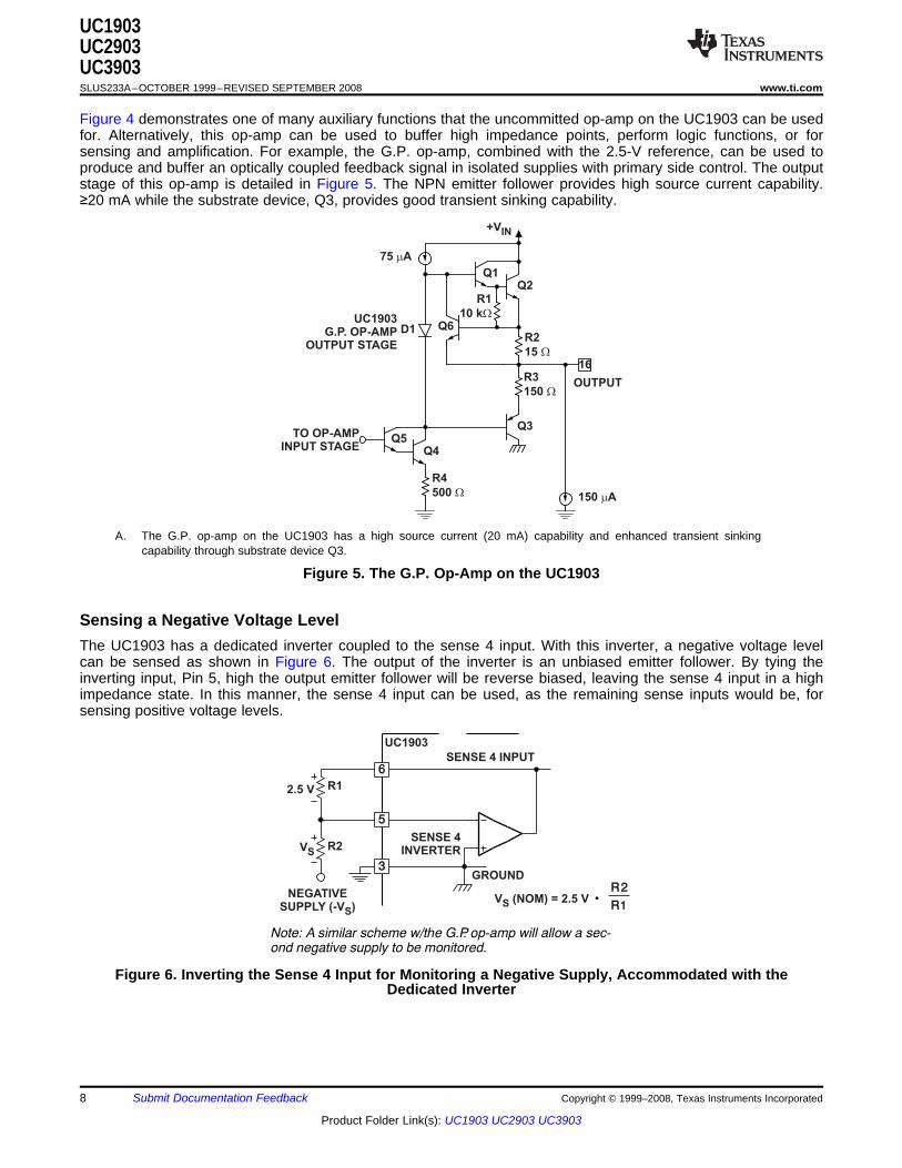
Figure 4 demonstrates one of many auxiliary functions that the uncommitted op-amp on the UC1903 can be usedfor. Alternatively, this op-amp can be used to buffer high impedance points, perform logic functions, or forsensing and amplification. For example, the G.P. op-amp, combined with the 2.5-V reference, can be used toproduce and buffer an optically coupled feedback signal in isolated supplies with primary side control. The outputstage of this op-amp is detailed in Figure 5. The NPN emitter follower provides high source current capability.≥20 mA while the substrate device, Q3, provides good transient sinking capability.
A. The G.P. op-amp on the UC1903 has a high source current (20 mA) capability and enhanced transient sinkingcapability through substrate device Q3.
Figure 5. The G.P. Op-Amp on the UC1903
The UC1903 has a dedicated inverter coupled to the sense 4 input. With this inverter, a negative voltage levelcan be sensed as shown in Figure 6. The output of the inverter is an unbiased emitter follower. By tying theinverting input, Pin 5, high the output emitter follower will be reverse biased, leaving the sense 4 input in a highimpedance state. In this manner, the sense 4 input can be used, as the remaining sense inputs would be, forsensing positive voltage levels.
Figure 6. Inverting the Sense 4 Input for Monitoring a Negative Supply, Accommodated with theDedicated Inverter
8 Submit Documentation Feedback Copyright © 1999–2008, Texas Instruments Incorporated
Product Folder Link(s): UC1903 UC2903 UC3903
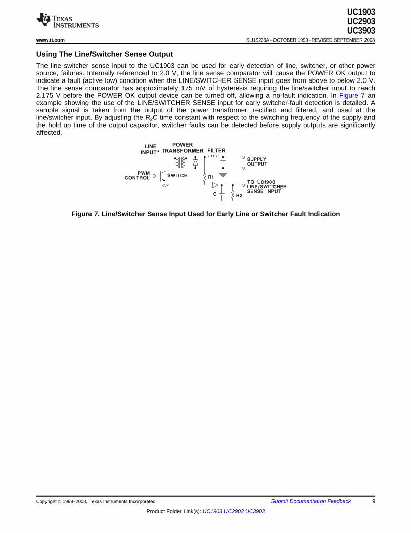
Using The Line/Switcher Sense Output
LINEINPUT
POWERTRANSFORMER FILTER
UC1903UC2903UC3903
www.ti.com ........................................................................................................................................ SLUS233A–OCTOBER 1999–REVISED SEPTEMBER 2008
The line switcher sense input to the UC1903 can be used for early detection of line, switcher, or other powersource, failures. Internally referenced to 2.0 V, the line sense comparator will cause the POWER OK output toindicate a fault (active low) condition when the LINE/SWITCHER SENSE input goes from above to below 2.0 V.The line sense comparator has approximately 175 mV of hysteresis requiring the line/switcher input to reach2.175 V before the POWER OK output device can be turned off, allowing a no-fault indication. In Figure 7 anexample showing the use of the LINE/SWITCHER SENSE input for early switcher-fault detection is detailed. Asample signal is taken from the output of the power transformer, rectified and filtered, and used at theline/switcher input. By adjusting the R2C time constant with respect to the switching frequency of the supply andthe hold up time of the output capacitor, switcher faults can be detected before supply outputs are significantlyaffected.
Figure 7. Line/Switcher Sense Input Used for Early Line or Switcher Fault Indication
Copyright © 1999–2008, Texas Instruments Incorporated Submit Documentation Feedback 9
Product Folder Link(s): UC1903 UC2903 UC3903

OV and UV Comparators Maintain Accurate Thresholds
6.4 V
Q1 Q2 Q3 Q4 Q5
Q6 Q7 Q8 Q9
Q10 Q11 Q12 Q13 Q14
Q15 Q16 Q17 Q18
OV COMPARATOR
UV COMPARATOR
SENSE 1
2 kW
R1
Z15.7 V
D1
SENSE 2
SENSE 3
SENSE 4
100 Am
6.4 V
50 Am
TO UVTHRESHOLD
VOLTAGE
OVHYSTERESIS
CONTROL
6.4 V
60 Am
Q20
Q19
1.8 V
TO OVTHRESHOLD
VOLTAGE
UVHYSTERESIS
CONTROL
6.4 V
60 Am
1.8 V
EXT.OV DELAYCAPACITOR
OV FAULTINDICATIONTO OUTPUTLOGIC
V
EXT.UV DELAYCAPACITOR
REF
UV FAULTINDICATIONTO OUTPUTLOGIC
Start Latch and Supply Under-Voltage Sense Allow Predictable Power-Up
UC1903UC2903UC3903SLUS233A–OCTOBER 1999–REVISED SEPTEMBER 2008 ........................................................................................................................................ www.ti.com
The structure of the OV and UV comparators, shown in Figure 8 results in accurate fault thresholds even in thecase where multiple sense inputs cross a fault threshold simultaneously. Unused sense inputs can be tied eitherto the 2.5-V reference, or to another, utilized, sense input. The four under- and over-voltage sense inputs on theUC1903 are clamped as detailed on the Sense 1 input in Figure 8. The series 2-kΩ resistor, R1, and zener diodeZ1, prevent extreme under- and over-voltage conditions from inverting the outputs of the fault comparators. Aparasitic diode, D1, is present at the inputs as well. Under normal operation it is advisable to insure that voltagelevels at all of the sense inputs stay above –0.3 V. The same type of input protection exists at the line senseinput, Pin 15, except a 5-kΩ series resistor is used.
The fault delay circuitry on the UC1903 is also shown in Figure 8. In the case of an over-voltage condition at oneof the sense inputs Q20 is turned off, allowing the internal 60-mA current source to charge the user-selecteddelay capacitor. When the capacitor voltage reaches 1.8 V, the OV and POWER OK outputs become active low.When the fault condition goes away Q20 is turned back on, rapidly discharging the delay capacitor. Operation ofthe under- voltage delay is, with appropriate substitutions, the same.
A. The OV and UV comparators on the UC1903 trigger respective fault delay circuits when one or more of the senseinputs move outside the fault window. Input clamps insure proper operation under extreme fault conditions.Terminating the UV delay capacitor to VREF assures correct logic at power up.
Figure 8. OV and UV Comparators on the UC1903
At power-Up, while the +VIN input supply is below 3 V, all open collector outputs are off. With +VIN greater than 3V the POWER OK output will be driven low and the UV OV FAULT outputs are disabled. Once +VIN rises abovethe VSUV threshold of 7 V the fault outputs will be enabled. As would be expected, the SENSE 1-4 voltages atpower up may be below the UVFAULT window and the UVFAULT output may be driven low.
10 Submit Documentation Feedback Copyright © 1999–2008, Texas Instruments Incorporated
Product Folder Link(s): UC1903 UC2903 UC3903
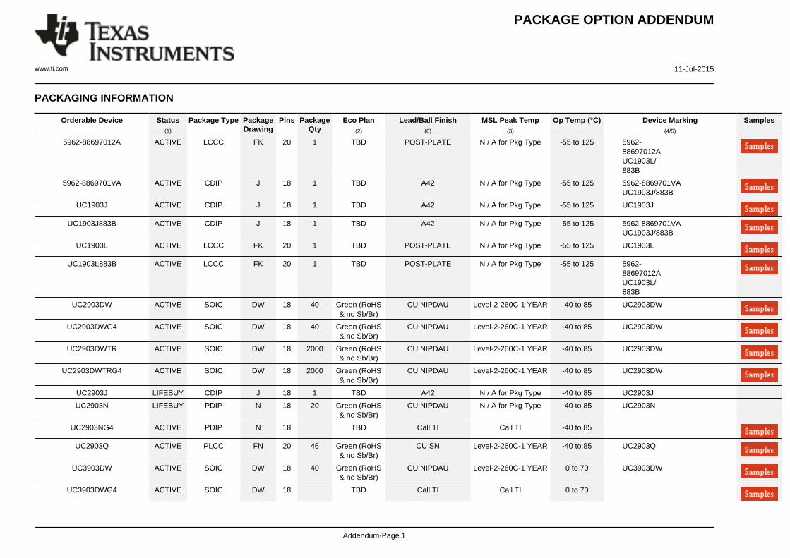
PACKAGE OPTION ADDENDUM
www.ti.com 11-Jul-2015
Addendum-Page 1
PACKAGING INFORMATION
Orderable Device Status(1)
Package Type PackageDrawing
Pins PackageQty
Eco Plan(2)
Lead/Ball Finish(6)
MSL Peak Temp(3)
Op Temp (°C) Device Marking(4/5)
Samples
5962-88697012A ACTIVE LCCC FK 20 1 TBD POST-PLATE N / A for Pkg Type -55 to 125 5962-88697012AUC1903L/883B
5962-8869701VA ACTIVE CDIP J 18 1 TBD A42 N / A for Pkg Type -55 to 125 5962-8869701VAUC1903J/883B
UC1903J ACTIVE CDIP J 18 1 TBD A42 N / A for Pkg Type -55 to 125 UC1903J
UC1903J883B ACTIVE CDIP J 18 1 TBD A42 N / A for Pkg Type -55 to 125 5962-8869701VAUC1903J/883B
UC1903L ACTIVE LCCC FK 20 1 TBD POST-PLATE N / A for Pkg Type -55 to 125 UC1903L
UC1903L883B ACTIVE LCCC FK 20 1 TBD POST-PLATE N / A for Pkg Type -55 to 125 5962-88697012AUC1903L/883B
UC2903DW ACTIVE SOIC DW 18 40 Green (RoHS& no Sb/Br)
CU NIPDAU Level-2-260C-1 YEAR -40 to 85 UC2903DW
UC2903DWG4 ACTIVE SOIC DW 18 40 Green (RoHS& no Sb/Br)
CU NIPDAU Level-2-260C-1 YEAR -40 to 85 UC2903DW
UC2903DWTR ACTIVE SOIC DW 18 2000 Green (RoHS& no Sb/Br)
CU NIPDAU Level-2-260C-1 YEAR -40 to 85 UC2903DW
UC2903DWTRG4 ACTIVE SOIC DW 18 2000 Green (RoHS& no Sb/Br)
CU NIPDAU Level-2-260C-1 YEAR -40 to 85 UC2903DW
UC2903J LIFEBUY CDIP J 18 1 TBD A42 N / A for Pkg Type -40 to 85 UC2903J
UC2903N LIFEBUY PDIP N 18 20 Green (RoHS& no Sb/Br)
CU NIPDAU N / A for Pkg Type -40 to 85 UC2903N
UC2903NG4 ACTIVE PDIP N 18 TBD Call TI Call TI -40 to 85
UC2903Q ACTIVE PLCC FN 20 46 Green (RoHS& no Sb/Br)
CU SN Level-2-260C-1 YEAR -40 to 85 UC2903Q
UC3903DW ACTIVE SOIC DW 18 40 Green (RoHS& no Sb/Br)
CU NIPDAU Level-2-260C-1 YEAR 0 to 70 UC3903DW
UC3903DWG4 ACTIVE SOIC DW 18 TBD Call TI Call TI 0 to 70

PACKAGE OPTION ADDENDUM
www.ti.com 11-Jul-2015
Addendum-Page 2
Orderable Device Status(1)
Package Type PackageDrawing
Pins PackageQty
Eco Plan(2)
Lead/Ball Finish(6)
MSL Peak Temp(3)
Op Temp (°C) Device Marking(4/5)
Samples
UC3903DWTR ACTIVE SOIC DW 18 2000 Green (RoHS& no Sb/Br)
CU NIPDAU Level-2-260C-1 YEAR 0 to 70 UC3903DW
UC3903DWTRG4 ACTIVE SOIC DW 18 2000 Green (RoHS& no Sb/Br)
CU NIPDAU Level-2-260C-1 YEAR 0 to 70 UC3903DW
UC3903J LIFEBUY CDIP J 18 1 TBD A42 N / A for Pkg Type 0 to 70 UC3903J
UC3903N LIFEBUY PDIP N 18 20 Green (RoHS& no Sb/Br)
CU NIPDAU N / A for Pkg Type 0 to 70 UC3903N
UC3903NG4 LIFEBUY PDIP N 18 20 Green (RoHS& no Sb/Br)
CU NIPDAU N / A for Pkg Type 0 to 70 UC3903N
UC3903Q ACTIVE PLCC FN 20 46 Green (RoHS& no Sb/Br)
CU SN Level-2-260C-1 YEAR 0 to 70 UC3903Q
UC3903QG3 ACTIVE PLCC FN 20 46 Green (RoHS& no Sb/Br)
CU SN Level-2-260C-1 YEAR 0 to 70 UC3903Q
(1) The marketing status values are defined as follows:ACTIVE: Product device recommended for new designs.LIFEBUY: TI has announced that the device will be discontinued, and a lifetime-buy period is in effect.NRND: Not recommended for new designs. Device is in production to support existing customers, but TI does not recommend using this part in a new design.PREVIEW: Device has been announced but is not in production. Samples may or may not be available.OBSOLETE: TI has discontinued the production of the device.
(2) Eco Plan - The planned eco-friendly classification: Pb-Free (RoHS), Pb-Free (RoHS Exempt), or Green (RoHS & no Sb/Br) - please check http://www.ti.com/productcontent for the latest availabilityinformation and additional product content details.TBD: The Pb-Free/Green conversion plan has not been defined.Pb-Free (RoHS): TI's terms "Lead-Free" or "Pb-Free" mean semiconductor products that are compatible with the current RoHS requirements for all 6 substances, including the requirement thatlead not exceed 0.1% by weight in homogeneous materials. Where designed to be soldered at high temperatures, TI Pb-Free products are suitable for use in specified lead-free processes.Pb-Free (RoHS Exempt): This component has a RoHS exemption for either 1) lead-based flip-chip solder bumps used between the die and package, or 2) lead-based die adhesive used betweenthe die and leadframe. The component is otherwise considered Pb-Free (RoHS compatible) as defined above.Green (RoHS & no Sb/Br): TI defines "Green" to mean Pb-Free (RoHS compatible), and free of Bromine (Br) and Antimony (Sb) based flame retardants (Br or Sb do not exceed 0.1% by weightin homogeneous material)
(3) MSL, Peak Temp. - The Moisture Sensitivity Level rating according to the JEDEC industry standard classifications, and peak solder temperature.
(4) There may be additional marking, which relates to the logo, the lot trace code information, or the environmental category on the device.
(5) Multiple Device Markings will be inside parentheses. Only one Device Marking contained in parentheses and separated by a "~" will appear on a device. If a line is indented then it is a continuationof the previous line and the two combined represent the entire Device Marking for that device.

PACKAGE OPTION ADDENDUM
www.ti.com 11-Jul-2015
Addendum-Page 3
(6) Lead/Ball Finish - Orderable Devices may have multiple material finish options. Finish options are separated by a vertical ruled line. Lead/Ball Finish values may wrap to two lines if the finishvalue exceeds the maximum column width.
Important Information and Disclaimer:The information provided on this page represents TI's knowledge and belief as of the date that it is provided. TI bases its knowledge and belief on informationprovided by third parties, and makes no representation or warranty as to the accuracy of such information. Efforts are underway to better integrate information from third parties. TI has taken andcontinues to take reasonable steps to provide representative and accurate information but may not have conducted destructive testing or chemical analysis on incoming materials and chemicals.TI and TI suppliers consider certain information to be proprietary, and thus CAS numbers and other limited information may not be available for release.
In no event shall TI's liability arising out of such information exceed the total purchase price of the TI part(s) at issue in this document sold by TI to Customer on an annual basis.
OTHER QUALIFIED VERSIONS OF UC1903, UC2903, UC2903M, UC3903, UC3903M :
• Catalog: UC3903, UC2903, UC3903M, UC3903
• Military: UC2903M, UC1903, UC1903
NOTE: Qualified Version Definitions:
• Catalog - TI's standard catalog product
• Military - QML certified for Military and Defense Applications
TAPE AND REEL INFORMATION
*All dimensions are nominal
Device PackageType
PackageDrawing
Pins SPQ ReelDiameter
(mm)
ReelWidth
W1 (mm)
A0(mm)
B0(mm)
K0(mm)
P1(mm)
W(mm)
Pin1Quadrant
UC2903DWTR SOIC DW 18 2000 330.0 24.4 10.9 12.0 2.7 12.0 24.0 Q1
UC3903DWTR SOIC DW 18 2000 330.0 24.4 10.9 12.0 2.7 12.0 24.0 Q1
PACKAGE MATERIALS INFORMATION
www.ti.com 11-Mar-2014
Pack Materials-Page 1
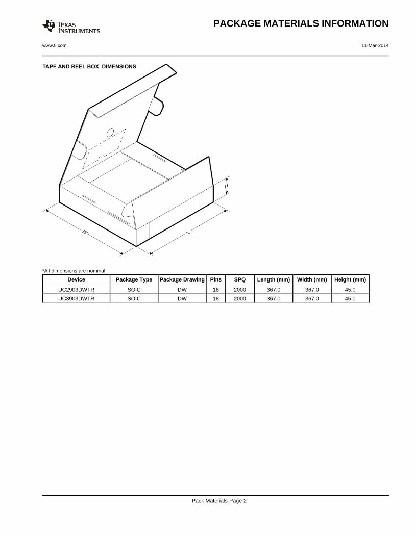
*All dimensions are nominal
Device Package Type Package Drawing Pins SPQ Length (mm) Width (mm) Height (mm)
UC2903DWTR SOIC DW 18 2000 367.0 367.0 45.0
UC3903DWTR SOIC DW 18 2000 367.0 367.0 45.0
PACKAGE MATERIALS INFORMATION
www.ti.com 11-Mar-2014
Pack Materials-Page 2

IMPORTANT NOTICE
Texas Instruments Incorporated and its subsidiaries (TI) reserve the right to make corrections, enhancements, improvements and otherchanges to its semiconductor products and services per JESD46, latest issue, and to discontinue any product or service per JESD48, latestissue. Buyers should obtain the latest relevant information before placing orders and should verify that such information is current andcomplete. All semiconductor products (also referred to herein as “components”) are sold subject to TI’s terms and conditions of salesupplied at the time of order acknowledgment.TI warrants performance of its components to the specifications applicable at the time of sale, in accordance with the warranty in TI’s termsand conditions of sale of semiconductor products. Testing and other quality control techniques are used to the extent TI deems necessaryto support this warranty. Except where mandated by applicable law, testing of all parameters of each component is not necessarilyperformed.TI assumes no liability for applications assistance or the design of Buyers’ products. Buyers are responsible for their products andapplications using TI components. To minimize the risks associated with Buyers’ products and applications, Buyers should provideadequate design and operating safeguards.TI does not warrant or represent that any license, either express or implied, is granted under any patent right, copyright, mask work right, orother intellectual property right relating to any combination, machine, or process in which TI components or services are used. Informationpublished by TI regarding third-party products or services does not constitute a license to use such products or services or a warranty orendorsement thereof. Use of such information may require a license from a third party under the patents or other intellectual property of thethird party, or a license from TI under the patents or other intellectual property of TI.Reproduction of significant portions of TI information in TI data books or data sheets is permissible only if reproduction is without alterationand is accompanied by all associated warranties, conditions, limitations, and notices. TI is not responsible or liable for such altereddocumentation. Information of third parties may be subject to additional restrictions.Resale of TI components or services with statements different from or beyond the parameters stated by TI for that component or servicevoids all express and any implied warranties for the associated TI component or service and is an unfair and deceptive business practice.TI is not responsible or liable for any such statements.Buyer acknowledges and agrees that it is solely responsible for compliance with all legal, regulatory and safety-related requirementsconcerning its products, and any use of TI components in its applications, notwithstanding any applications-related information or supportthat may be provided by TI. Buyer represents and agrees that it has all the necessary expertise to create and implement safeguards whichanticipate dangerous consequences of failures, monitor failures and their consequences, lessen the likelihood of failures that might causeharm and take appropriate remedial actions. Buyer will fully indemnify TI and its representatives against any damages arising out of the useof any TI components in safety-critical applications.In some cases, TI components may be promoted specifically to facilitate safety-related applications. With such components, TI’s goal is tohelp enable customers to design and create their own end-product solutions that meet applicable functional safety standards andrequirements. Nonetheless, such components are subject to these terms.No TI components are authorized for use in FDA Class III (or similar life-critical medical equipment) unless authorized officers of the partieshave executed a special agreement specifically governing such use.Only those TI components which TI has specifically designated as military grade or “enhanced plastic” are designed and intended for use inmilitary/aerospace applications or environments. Buyer acknowledges and agrees that any military or aerospace use of TI componentswhich have not been so designated is solely at the Buyer's risk, and that Buyer is solely responsible for compliance with all legal andregulatory requirements in connection with such use.TI has specifically designated certain components as meeting ISO/TS16949 requirements, mainly for automotive use. In any case of use ofnon-designated products, TI will not be responsible for any failure to meet ISO/TS16949.
Products ApplicationsAudio www.ti.com/audio Automotive and Transportation www.ti.com/automotiveAmplifiers amplifier.ti.com Communications and Telecom www.ti.com/communicationsData Converters dataconverter.ti.com Computers and Peripherals www.ti.com/computersDLP® Products www.dlp.com Consumer Electronics www.ti.com/consumer-appsDSP dsp.ti.com Energy and Lighting www.ti.com/energyClocks and Timers www.ti.com/clocks Industrial www.ti.com/industrialInterface interface.ti.com Medical www.ti.com/medicalLogic logic.ti.com Security www.ti.com/securityPower Mgmt power.ti.com Space, Avionics and Defense www.ti.com/space-avionics-defenseMicrocontrollers microcontroller.ti.com Video and Imaging www.ti.com/videoRFID www.ti-rfid.comOMAP Applications Processors www.ti.com/omap TI E2E Community e2e.ti.comWireless Connectivity www.ti.com/wirelessconnectivity
Mailing Address: Texas Instruments, Post Office Box 655303, Dallas, Texas 75265Copyright © 2015, Texas Instruments Incorporated