quantitative measurement of the effectiveness of ... · pdf filethe quantitative measurement...
TRANSCRIPT

25th Annual Passive Components Conference – CARTS 2005 USA March 21 – 24, 2005 – Palm Springs, CA
The Quantitative Measurement of the Effectiveness of Decoupling Capacitors in Controlling Switching Transients from Microprocessors
Dale L. Sanders James P. Muccioli X2Y Attenuators, LLC
37554 Hills Tech Dr. Farmington Hills, MI 48331
248-489-0007 248-489-9305 (Fax)
X2Y Attenuators, LLC 37554 Hills Tech Dr.
Farmington Hills, MI 48331 248-489-0007
248-489-9305 (Fax) [email protected]
Terry M. North Kevin P. Slattery DaimlerChrysler
800 Chrysler Drive Auburn Hills, MI 48326
248-576-5854 248-576-2265(Fax)
Intel Corporation JF2-54, 2111 N.E, 25th Avenue
Hillsboro, OR 97124-5961 503-264-8358
503-264-6053(Fax) [email protected]
ABSTRACT
Power distribution systems (PDS) are typically comprised of capacitor networks that have several types of capacitors and values to obtain a targeted impedance over the required frequency spectrum for the PDS planes on a printed circuit board (PCB). Capacitors serve two primary roles in meeting the targeted impedance. The first role is to provide a temporary source of localized energy for instantaneous current demands from an IC; the second is to provide a low-impedance return path for high frequency noise. This paper proposes a time-domain test to evaluate a capacitor’s performance and effectiveness to meet these two primary roles.
INTRODUCTION
Currently there is no known (to the authors) or agreed-upon industry standard to evaluate the performance and effectiveness of capacitors in a time-domain or frequency analysis. Several technical conferences have devoted entire sections to discuss this issue, [1], [2], and [3]. The authors of this paper look to document several parameters of a time-domain analysis that could be proposed in a future standardized test methodology for measuring and evaluating capacitors.
The amount of energy, or more specifically, current that a capacitor supplies across its terminals can be
defined by Equation 1. In a time-domain analysis, Equation 1 can be useful in representing the individual elements that affect current in a bypass capacitor (Figure 1). For example, the change in voltage (dv) represents the change of voltage amplitude across the capacitor, the change in time (dt) represents the length of the period for this change (frequency), and the change in voltage over the change in time (dv/dt) represents the rise/fall time (switching frequency).
dttdvCti )()( = (1)
Figure 1. A bypass capacitor is a line-to-ground (return) circuit element.
However, Equation 1 assumes a constant C (capacitance) value which implies an ideal capacitor. A typical capacitor model, shown in Figure 2, illustrates that a non-ideal capacitor has an associated parasitic resistance and inductance which affects a capacitor’s ability to supply current.
1

25th Annual Passive Components Conference – CARTS 2005 USA March 21 – 24, 2005 – Palm Springs, CA
Figure 2. Typical model of a non-ideal capacitor.
Equations 2 represent the characteristic impedance of the model in Figure 2. The parasitic resistance (R) is assumed to be constant, while the parasitic reactance (L and C) is frequency dependant. As frequency increase the contribution of C decreases, while the contribution of L increases.
CjLjRZCapacitor ω
ω −+= (2)
where: ω = 2πf
f = 1/period
If the amount of current drawn and the switching frequency of an IC are known, then Equation 1 can be used to approximate the total required capacitance value for a PDS. However, since that target is required over a broad frequency, the contribution of R and the reactance of L need to be addressed. Typically, R is fairly constant and is usually relatively small when compared to overall reactance L (which dominates Equation 2 as frequency increases). Therefore L is generally considered the critical factor when evaluating the performance of capacitors.
Inductance (L) of a capacitor is inherent to the physical size of the current loop it creates in a circuit. This means that the physical package size of a capacitor is typically the most important factor in determining the value of L. (Note: there are capacitor technologies that are exceptions to this which are briefly highlighted in the data of this paper.)
Reducing a capacitors’ package size to reduce the current loop, thus inductance (L), can introduce other issues. Smaller packages reduce the amount of layers (surface area) a capacitor can have internally, thus limiting the amount of capacitance (C) a single capacitor can have. In order to meet the total capacitance requirements estimated from Equation 1, multiple capacitors in parallel (capacitor networks) are required. With today’s current demands of ICs multiple parallel capacitors create issues such as PCB space, increased via count that limits routing, and PCB spreading and mounting inductance to name a few. [4]
EXPERIMENT SET-UP
The following time-domain analysis and supporting data highlights the effectiveness of a capacitor by varying each parameter in Equation 1.
The test fixture for this analysis uses a one layer (no ground-plane), FR-4 dielectric, 0.062” thick coplanar PCBs that are approximately 5/8” long with SMA end-launches on either ends. The current loop of the capacitor, device-under-test (DUT), was used to determine whether the fixture has an upper and lower “ground” trace. (For example, a standard MLCC surface mount capacitor would only have a lower trace, while an array capacitor such as an IDCTM or X2Y® component would have both an upper and lower trace.) Therefore, each DUT tested has a specifically designed coplanar PCB fixture to accommodate the different landpad layouts and current loop for the different package sizes and capacitor types. (Layouts for the landpads where obtained from manufacturer’s data sheets.) Table 1 is a complete list of DUTs examined in this paper.
Table 1. DUTs tested in this paper.
Type
Volt. Rating (VDC) Dielectric Package
Aluminum electrolytic Capacitor 50 AL EL BAluminum electrolytic Capacitor 50 AL EL BAluminum electrolytic Capacitor 50 AL EL CAluminum electrolytic Capacitor 50 AL EL DAluminum electrolytic Capacitor 50 AL EL GAluminum electrolytic Capacitor 50 AL EL G
Tantalum Chip Capacitor 16 Tan ATantalum Chip Capacitor 16 Tan ATantalum Chip Capacitor 16 Tan ATantalum Chip Capacitor 16 Tan BTantalum Chip Capacitor 16 Tan DTantalum Chip Capacitor 16 Tan D
MLCC 10 Y5V 0603MLCC 16 Y5V 0805MLCC 10 Y5V 0805MLCC 10 Y5V 1206MLCC 6.3 X5R 1210MLCC 6.3 X5R 1812MLCC 16 X7R 0603
InterDigitated Capacitors (IDC) MLCC 10 Y5V 0612InterDigitated Capacitors (IDC) MLCC 10 X5R 0612
Reverse Aspect Ratio, MLCC (Low-inductance) 10 Y5V 0306Reverse Aspect Ratio, MLCC (Low-inductance) 10 X5R 0508Reverse Aspect Ratio, MLCC (Low-inductance) 16 X5R 0612
Rated TotalX2Y MLCC 0.47 0.94 16 X7R 1206X2Y MLCC 0.56 1.12 25 X7R 1210X2Y MLCC 0.47 0.94 63 X7R 1812X2Y MLCC 0.82 1.64 10 X7R 1206X2Y MLCC 0.82 1.64 16 X7R 1210X2Y MLCC 1.0 2.0 25 X7R 1812X2Y MLCC 5.0 10 10 Y5V 1210X2Y MLCC 6.5 13 16 Y5V 1210
10047104.7
1.00.1
2.21.0
10047104.7
2.21.0
1.01.0
0.222.2
Cap. Value (uF)
10047104.72.21.0
To verify the 50 ohm characteristic of the PCB coplanar fixtures (50 ohms = 0dB insertion loss), insertion loss measurements were taken with an Agilent E5071A ENA network analyzer using an S21 measurement. Results are highlighted in Table 2.
2
25th Annual Passive Components Conference – CARTS 2005 USA March 21 – 24, 2005 – Palm Springs, CA
Table 2. Insertion Loss characteristics of the coplanar PCB fixtures.
Frequency Insertion Loss (dB)
300 kHz – 1 GHz ≤ 0.6dB
1 GHz – 5 GHz ≤ 4dB
5 GHz – 8.5 GHz ≤ 12.5dB
3
Once the DUTs were soldered to the PCB fixtures, insertion loss measurements were repeated to show the performance of the DUTs over frequency. (These results are shown later in the paper.)
Figure 3. Pictures of PCB fixtures with DUTs attached.
The time-domain analysis consists of digital inputs from a HP 8082A pulse generator connected to one SMA end-launch. The other SMA end-launch is connected to a Tektronix TDS 3054 oscilloscope which displays the resulting AC content.
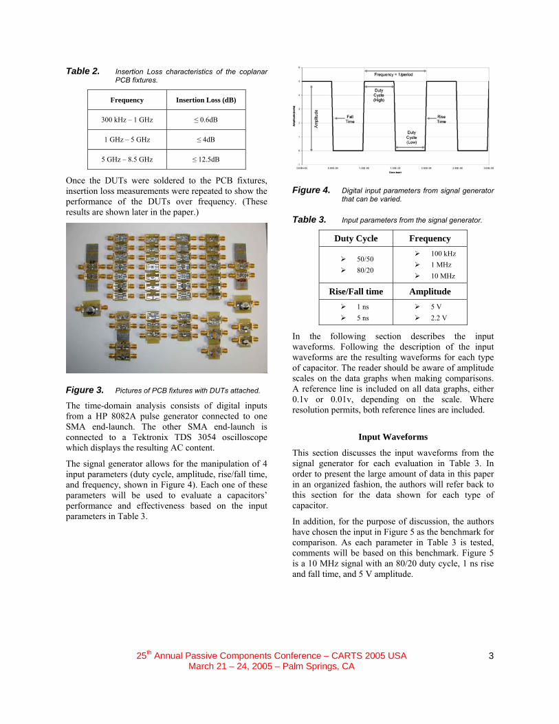
The signal generator allows for the manipulation of 4 input parameters (duty cycle, amplitude, rise/fall time, and frequency, shown in Figure 4). Each one of these parameters will be used to evaluate a capacitors’ performance and effectiveness based on the input parameters in Table 3.
Figure 4. Digital input parameters from signal generator that can be varied.
Table 3. Input parameters from the signal generator.
Duty Cycle Frequency
50/50 80/20
100 kHz 1 MHz 10 MHz
Rise/Fall time Amplitude 1 ns 5 ns
5 V 2.2 V
In the following section describes the input waveforms. Following the description of the input waveforms are the resulting waveforms for each type of capacitor. The reader should be aware of amplitude scales on the data graphs when making comparisons. A reference line is included on all data graphs, either 0.1v or 0.01v, depending on the scale. Where resolution permits, both reference lines are included.
Input Waveforms
This section discusses the input waveforms from the signal generator for each evaluation in Table 3. In order to present the large amount of data in this paper in an organized fashion, the authors will refer back to this section for the data shown for each type of capacitor.
In addition, for the purpose of discussion, the authors have chosen the input in Figure 5 as the benchmark for comparison. As each parameter in Table 3 is tested, comments will be based on this benchmark. Figure 5 is a 10 MHz signal with an 80/20 duty cycle, 1 ns rise and fall time, and 5 V amplitude.

25th Annual Passive Components Conference – CARTS 2005 USA March 21 – 24, 2005 – Palm Springs, CA
Figure 5. Benchmark input waveform.
Figure 6 is used to examine the effects of a slower rise and fall time on the performance of capacitors. The signal is a 10 MHz signal with an 80/20 duty cycle, 5 ns rise and fall time, and 5 V amplitude.
Figure 6. Input waveform used to examine the effects of 5 ns vs. 1 ns rise and fall time (Figure 5).
Figure 7 is used to examine the effects of a 50/50 duty cycle on the performance of capacitors. The signal is a 10 MHz signal with a 50/50 duty cycle, 1 ns rise and fall time, and 5 V amplitude.
Figure 7. Input waveform used to examine the effects of a 50/50 vs. an 80/20 duty cycle (Figure 5).
Figure 8 is used to examine the effects of a 2.2 V Amplitude on the performance of capacitors. The
signal is a 10 MHz signal with an 80/20 duty cycle, 1 ns rise and fall time, and 2.2 V amplitude.
Figure 8. Input waveform used to examine the effects of 2.2 V amplitude vs. 5 V amplitude (Figure 5).
Figure 9 is used to examine the effects of frequency on the performance of capacitors. The signal is a 1 MHz signal with an 80/20 duty cycle, 1 ns rise and fall time, and 5 V amplitude.
Figure 9. Input waveform used to examine the effects of 1 MHz vs. 10 MHz frequency (Figure 5).
Figure 10 is used to continue the examination of the effects of frequency on the performance of capacitors. The signal is a 100 kHz signal with an 80/20 duty cycle, 5 ns rise and fall time, and 5 V amplitude.
4

25th Annual Passive Components Conference – CARTS 2005 USA March 21 – 24, 2005 – Palm Springs, CA
Figure 10. Input waveform used to examine the effects of 100 kHz vs. 10 MHz frequency (Figure 5). NOTE: due to equipment limitations, the rise and fall time was set to 5 ns instead of 1 ns as in Figure 5.
Electrolytic Capacitors
Figure 11 is the insertion loss measurements of the electrolytic capacitors from 300 kHz to 8.5 GHz. The larger the capacitive value the more attenuation occurs at the lower frequencies. The trade off, however, for more capacitance is a larger package size (more internal layers/surface area) which increases overall inductance. The increase in overall inductance impairs the performance at higher frequencies.
Figure 11. Insertion Loss of electrolytic capacitors.
Figure 12 – Figure 17 are the electrolytic response to the input waveforms (Figure 5 – Figure 10). Figure 12 is the baseline response. Comparing a 1 ns rise/fall time (Figure 12) to a 5 ns rise/fall time (Figure 13) significantly reduces the overshoot and undershoot transients. It should also be noted that in Figure 12 as the package size increase from B to G the overshoot and undershoot transients also increase.
Figure 12. Electrolytic capacitor results of 10 MHz, 80/20 duty cycle, 1 ns rise/fall time, 5 V amplitude input waveform. (See input waveform in Figure 5.)
Figure 13. Electrolytic capacitor results of 10 MHz, 80/20 duty cycle, 5 ns rise/fall time, 5 V amplitude input waveform. (See input waveform in Figure 6.)
Comparing an 80/20 duty cycle (Figure 12) to a 50/50 duty cycle (Figure 14) yields a slight decrease in the negative ripple, but a significant increase in the positive ripple. However, in both cases the ripple decreases as the capacitance value increases.
Figure 14. Electrolytic capacitor results of 10 MHz, 50/50 duty cycle, 1 ns rise/fall time, 5 V amplitude input waveform. (See input waveform in Figure 7.)
5
25th Annual Passive Components Conference – CARTS 2005 USA March 21 – 24, 2005 – Palm Springs, CA
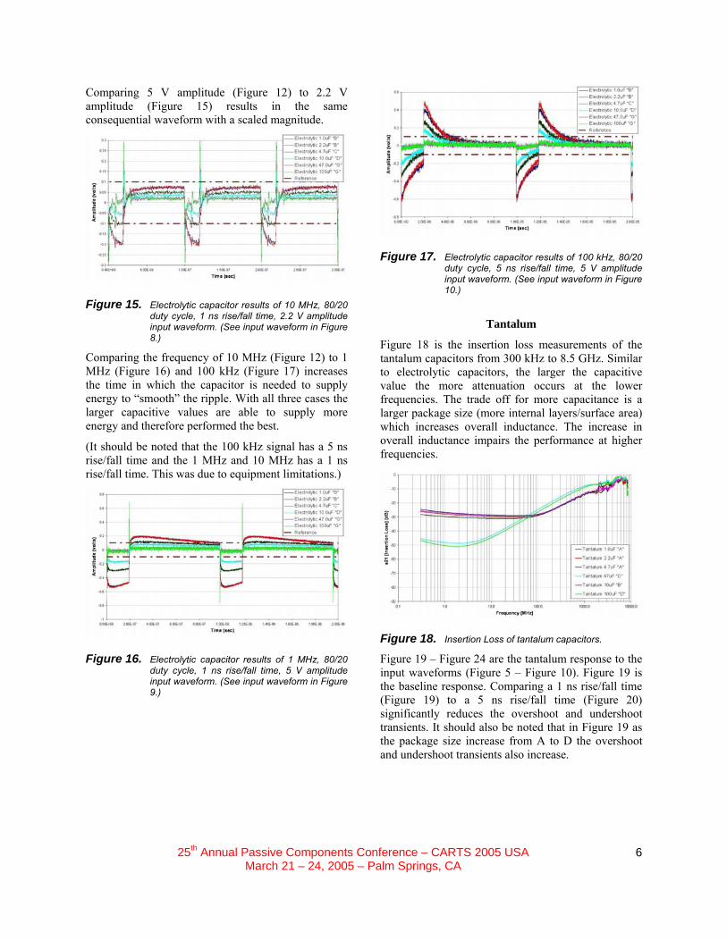
Comparing 5 V amplitude (Figure 12) to 2.2 V amplitude (Figure 15) results in the same consequential waveform with a scaled magnitude.
Figure 15. Electrolytic capacitor results of 10 MHz, 80/20 duty cycle, 1 ns rise/fall time, 2.2 V amplitude input waveform. (See input waveform in Figure 8.)
Comparing the frequency of 10 MHz (Figure 12) to 1 MHz (Figure 16) and 100 kHz (Figure 17) increases the time in which the capacitor is needed to supply energy to “smooth” the ripple. With all three cases the larger capacitive values are able to supply more energy and therefore performed the best.
(It should be noted that the 100 kHz signal has a 5 ns rise/fall time and the 1 MHz and 10 MHz has a 1 ns rise/fall time. This was due to equipment limitations.)
Figure 16. Electrolytic capacitor results of 1 MHz, 80/20 duty cycle, 1 ns rise/fall time, 5 V amplitude input waveform. (See input waveform in Figure 9.)
Figure 17. Electrolytic capacitor results of 100 kHz, 80/20 duty cycle, 5 ns rise/fall time, 5 V amplitude input waveform. (See input waveform in Figure 10.)
Tantalum
Figure 18 is the insertion loss measurements of the tantalum capacitors from 300 kHz to 8.5 GHz. Similar to electrolytic capacitors, the larger the capacitive value the more attenuation occurs at the lower frequencies. The trade off for more capacitance is a larger package size (more internal layers/surface area) which increases overall inductance. The increase in overall inductance impairs the performance at higher frequencies.
Figure 18. Insertion Loss of tantalum capacitors.
Figure 19 – Figure 24 are the tantalum response to the input waveforms (Figure 5 – Figure 10). Figure 19 is the baseline response. Comparing a 1 ns rise/fall time (Figure 19) to a 5 ns rise/fall time (Figure 20) significantly reduces the overshoot and undershoot transients. It should also be noted that in Figure 19 as the package size increase from A to D the overshoot and undershoot transients also increase.
6

25th Annual Passive Components Conference – CARTS 2005 USA March 21 – 24, 2005 – Palm Springs, CA
Figure 19. Tantalum capacitor results of 10 MHz, 80/20 duty cycle, 1 ns rise/fall time, 5 V amplitude input waveform. (See input waveform in Figure 5.)
Figure 20. Tantalum capacitor results of 10 MHz, 80/20 duty cycle, 5 ns rise/fall time, 5 V amplitude input waveform. (See input waveform in Figure 6.)
Comparing an 80/20 duty cycle (Figure 19) to a 50/50 duty cycle (Figure 21) yields a slight decrease in the negative ripple, but a significant increase in the positive ripple. However, in both cases the ripple decreases as the capacitance value increases.
Figure 21. Tantalum capacitor results of 10 MHz, 50/50 duty cycle, 1 ns rise/fall time, 5 V amplitude input waveform. (See input waveform in Figure 7.)
Comparing 5 V amplitude (Figure 19) to 2.2 V amplitude (Figure 22) results in the same consequential waveform with a scaled magnitude.
Figure 22. Tantalum capacitor results of 10 MHz, 80/20 duty cycle, 1 ns rise/fall time, 2.2 V amplitude input waveform. (See input waveform in Figure 8.)
Comparing the frequency of 10 MHz (Figure 19) to 1 MHz (Figure 23) and 100 kHz (Figure 24) increase the time in which the capacitor is needed to supply energy to “smooth” the ripple. With all three cases the larger capacitive values are able to supply more energy and therefore performed the best.
(It should be noted that the 100 kHz signal has a 5 ns rise/fall time and the 1 MHz and 10 MHz has a 1 ns rise/fall time. This was due to equipment limitations.)
Figure 23. Tantalum capacitor results of 1 MHz, 80/20 duty cycle, 1 ns rise/fall time, 5 V amplitude input waveform. (See input waveform in Figure 9.)
7

25th Annual Passive Components Conference – CARTS 2005 USA March 21 – 24, 2005 – Palm Springs, CA
Figure 24. Tantalum capacitor results of 100 kHz, 80/20 duty cycle, 5 ns rise/fall time, 5 V amplitude input waveform. (See input waveform in Figure 10.)
Standard MLCC
Figure 25 is the insertion loss measurements of the standard MLCC capacitors from 300 kHz to 8.5 GHz. For standard MLCC, inductance is not dependant on just package length (current loop), but also package width. The length to width package ratio is what should be used to calculate inductance. With that said, the length remains the predominant factor and typically the smaller the package (package length), the lower the overall inductance.
Figure 25. Insertion Loss of MLCC.
Figure 26 – Figure 31 are the MLCC response to the input waveforms (Figure 5 – Figure 10). Figure 26 is the baseline response. Comparing a 1 ns rise/fall time (Figure 26) to a 5 ns rise/fall time (Figure 27) significantly reduces the overshoot and undershoot transients. It should also be noted that in Figure 26 as the package size increase from 0603 to 1812 the overshoot and undershoot transients also increase.
Figure 26. MLCC capacitor results of 10 MHz, 80/20 duty cycle, 1 ns rise/fall time, 5 V amplitude input waveform. (See input waveform in Figure 5.)
Figure 27. MLCC capacitor results of 10 MHz, 80/20 duty cycle, 5 ns rise/fall time, 5 V amplitude input waveform. (See input waveform in Figure 6.)
Comparing an 80/20 duty cycle (Figure 26) to a 50/50 duty cycle (Figure 28) yields a slight decrease in the negative ripple, but a significant increase in the positive ripple. Like the tantalum and electrolytic capacitors the ripple decreases as the capacitance value increases, however the MLCC were able to “smooth” the ripple with much less capacitance (2.2 uF compared to 47 uF for the tantalum and electrolytic).
Figure 28. MLCC capacitor results of 10 MHz, 50/50 duty cycle, 1 ns rise/fall time, 5 V amplitude input waveform. (See input waveform in Figure 7.)
8

25th Annual Passive Components Conference – CARTS 2005 USA March 21 – 24, 2005 – Palm Springs, CA
Comparing 5 V amplitude (Figure 26) to 2.2 V amplitude (Figure 29) results in the same consequential waveform with a scaled magnitude.
Figure 29. MLCC capacitor results of 10 MHz, 80/20 duty cycle, 1ns rise/fall time, 2.2v amplitude input waveform. (See input waveform in Figure 8.)
Comparing the frequency of 10 MHz (Figure 26) to 1 MHz (Figure 30) and 100 kHz (Figure 31) increase the time in which the capacitor is needed to supply energy to “smooth” the ripple. With all three cases the larger capacitive values are able to supply more energy and therefore performed the best.
(It should be noted that the 100 kHz signal has a 5 ns rise/fall time and the 1 MHz and 10 MHz has a 1 ns rise/fall time. This was due to equipment limitations.)
Figure 30. MLCC capacitor results of 1 MHz, 80/20 duty cycle, 1 ns rise/fall time, 5 V amplitude input waveform. (See input waveform in Figure 9.)
Figure 31. MLCC capacitor results of 100 kHz, 80/20 duty cycle, 5 ns rise/fall time, 5 V amplitude input waveform. (See input waveform in Figure 10.)
Reverse Aspect Ratio MLCC
(Low-inductance, LL)
Figure 32 is the insertion loss measurements of the reverse aspect ratio (LL) MLCC capacitors from 300 kHz to 8.5 GHz. LL MLCC capacitors take advantage of package length to width ratio to reduce inductance over standard MLCCs.
Figure 32. Insertion Loss of LL MLCC.
Figure 33 – Figure 38 are the LL MLCC response to the input waveforms (Figure 5 – Figure 10). Figure 33 is the baseline response. Comparing a 1 ns rise/fall time (Figure 33) to a 5 ns rise/fall time (Figure 34) significantly reduces the overshoot and undershoot transients. It should also be noted that in Figure 33 as the package size increase from 0306 to 0612 the overshoot and undershoot transients also increase.
9

25th Annual Passive Components Conference – CARTS 2005 USA March 21 – 24, 2005 – Palm Springs, CA
Figure 33. LL MLCC capacitor results of 10 MHz, 80/20 duty cycle, 1 ns rise/fall time, 5 V amplitude input waveform. (See input waveform in Figure 5.)
Figure 34. LL MLCC capacitor results of 10 MHz, 80/20 duty cycle, 5 ns rise/fall time, 5 V amplitude input waveform. (See input waveform in Figure 6.)
Comparing an 80/20 duty cycle (Figure 33) to a 50/50 duty cycle (Figure 35) yields a very slight decrease in the negative ripple and slight but noticeable increase in the positive ripple. However, it should be noted that the amount of capacitance needed is further reduced from standard MLCCs (2.2 uF to 1.0 uF).
Figure 35. LL MLCC capacitor results of 10 MHz, 50/50 duty cycle, 1 ns rise/fall time, 5 V amplitude input waveform. (See input waveform in Figure 7.)
Comparing 5 V amplitude (Figure 33) to 2.2 V amplitude (Figure 36) results in the same consequential waveform with a scaled magnitude.
Figure 36. LL MLCC capacitor results of 10 MHz, 80/20 duty cycle, 1 ns rise/fall time, 2.2 V amplitude input waveform. (See input waveform in Figure 8.)
Comparing the frequency of 10 MHz (Figure 33) to 1 MHz (Figure 37) and 100 kHz (Figure 38) increase the time in which the capacitor is needed to supply energy to “smooth” the ripple. With all three cases the larger capacitive values are able to supply more energy and therefore performed the best.
(It should be noted that the 100 kHz signal has a 5 ns rise/fall time and the 1 MHz and 10 MHz has a 1 ns rise/fall time. This was due to equipment limitations.)
Figure 37. LL MLCC capacitor results of 1 MHz, 80/20 duty cycle, 1 ns rise/fall time, 5 V amplitude input waveform. (See input waveform in Figure 9.)
10

25th Annual Passive Components Conference – CARTS 2005 USA March 21 – 24, 2005 – Palm Springs, CA
Figure 38. LL MLCC capacitor results of 100 kHz, 80/20 duty cycle, 5 ns rise/fall time, 5 V amplitude input waveform. (See input waveform in Figure 10.)
InterDigitated Components (IDCTM) MLCC
Figure 39 is the insertion loss measurements of the IDCTM MLCC capacitors from 300 kHz to 8.5 GHz. In order to lower the inductance at higher frequencies, the IDCTM structure promotes mutual inductance cancellation. This is accomplished by opposing current flow and alternating power/ground terminal arrangement.
Figure 39. Insertion Loss of IDCTM MLCC.
Figure 40 – Figure 45 are the IDCTM response to the input waveforms (Figure 5 – Figure 10). Figure 40 is the baseline response. Comparing a 1 ns rise/fall time (Figure 40) to a 5 ns rise/fall time (Figure 41) significantly reduces the overshoot and undershoot transients. It should also be noted that in Figure 40 as the capacitive value increases from 1.0 uF to 2.2 uF the overshoot and undershoot transients decrease.
Figure 40. IDCTM MLCC capacitor results of 10 MHz, 80/20 duty cycle, 1 ns rise/fall time, 5 V amplitude input waveform. (See input waveform in Figure 5.)
Figure 41. IDCTM MLCC capacitor results of 10 MHz, 80/20 duty cycle, 5 ns rise/fall time, 5 V amplitude input waveform. (See input waveform in Figure 6.)
Comparing an 80/20 duty cycle (Figure 40) to a 50/50 duty cycle (Figure 42) yields a very slight decrease in the negative ripple and slight but noticeable increase in the positive ripple. However, it should be noted here that the 1.0 uF IDCTM was able to further reduced the amplitude of the ripple over LL MLCC.
Figure 42. IDCTM MLCC capacitor results of 10 MHz, 50/50 duty cycle, 1 ns rise/fall time, 5 V amplitude input waveform. (See input waveform in Figure 7.)
11

25th Annual Passive Components Conference – CARTS 2005 USA March 21 – 24, 2005 – Palm Springs, CA
Comparing 5 V amplitude (Figure 40) to 2.2 V amplitude (Figure 43) results in the same consequential waveform with a scaled magnitude.
Figure 43. IDCTM MLCC capacitor results of 10 MHz, 80/20 duty cycle, 1 ns rise/fall time, 2.2 V amplitude input waveform. (See input waveform in Figure 8.)
Comparing the frequency of 10 MHz (Figure 40) to 1 MHz (Figure 44) and 100 kHz (Figure 45) increase the time in which the capacitor is needed to supply energy to “smooth” the ripple. With all three cases the larger capacitive values are able to supply more energy and therefore performed the best.
(It should be noted that the 100 kHz signal has a 5 ns rise/fall time and the 1 MHz and 10 MHz has a 1 ns rise/fall time. This was due to equipment limitations.)
Figure 44. IDCTM MLCC capacitor results of 1 MHz, 80/20 duty cycle, 1 ns rise/fall time, 5 V amplitude input waveform. (See input waveform in Figure 9.)
Figure 45. IDCTM MLCC capacitor results of 100 kHz, 80/20 duty cycle, 1ns rise/fall time, 5v amplitude input waveform. (See input waveform in Figure 10.)
X2Y® MLCC
Figure 46 is the insertion loss measurements of the X2Y® MLCC capacitors from 300 kHz to 8.5 GHz. The X2Y® Technology uses mutual inductance cancellation to lower overall inductance for higher frequency performance. The X2Y® Technology has two main benefits over other MLCC technology that uses mutual inductance cancellation. First, the X2Y® Technology is an open license technology which allows for multiple sources and second is the structure/termination locations. The most common X2Y® package has 4 terminations (although 6 and 8 terminations are available) and can be made in any package size, dielectric, or capacitive value.
(It should be noted that the X2Y® circuit configuration in this paper is Circuit 2. The capacitance values listed in the figure legends is the rated capacitance (line-to-ground, A or B to G1/G2). The total amount of capacitance X2Y® supplies in a Circuit 2 configuration is twice the rated capacitance. For a more information or broader definition of Circuit 2 and other circuit configurations see [5].)
Figure 46. Insertion Loss of X2Y® MLCC.
12
25th Annual Passive Components Conference – CARTS 2005 USA March 21 – 24, 2005 – Palm Springs, CA
Figure 47 – Figure 52 are the X2Y® response to the input waveforms (Figure 5 – Figure 10). Figure 47 is the baseline response. Comparing a 1 ns rise/fall time (Figure 47) to a 5 ns rise/fall time (Figure 48) significantly reduces the overshoot and undershoot transients. It should also be noted that in Figure 40 as the capacitive value increases the overshoot and undershoot transients decrease. Additionally, as the package size increases overshoot and undershoot transients decrease. This is contrary to other MLCC technology.
Figure 47. X2Y® MLCC capacitor results of 10 MHz, 80/20 duty cycle, 1 ns rise/fall time, 5 V amplitude input waveform. (See input waveform in Figure 5.)
Figure 48. X2Y® MLCC capacitor results of 10 MHz, 80/20 duty cycle, 5 ns rise/fall time, 5 V amplitude input waveform. (See input waveform in Figure 6.)
Comparing an 80/20 duty cycle (Figure 47) to a 50/50 duty cycle (Figure 49) yields a very slight decrease in the negative ripple and slight but noticeable increase in the positive ripple. However, it should be noted here that the results are comparable to the IDCTM results in Figure 42. Both the X2Y® and the IDCTM require less capacitance than other capacitor technologies to “smooth” the ripple.
Figure 49. X2Y® MLCC capacitor results of 10 MHz, 50/50 duty cycle, 1 ns rise/fall time, 5 V amplitude input waveform. (See input waveform in Figure 7.)
Comparing 5 V amplitude (Figure 47) to 2.2 V amplitude (Figure 50) results in the same consequential waveform with a scaled magnitude.
Figure 50. X2Y® MLCC capacitor results of 10 MHz, 80/20 duty cycle, 1 ns rise/fall time, 2.2 V amplitude input waveform. (See input waveform in Figure 8.)
Comparing the frequency of 10 MHz (Figure 47) to 1 MHz (Figure 51) and 100 kHz (Figure 52) increase the time in which the capacitor is needed to supply energy to “smooth” the ripple. With all three cases the larger capacitive values are able to supply more energy and therefore performed the best. However, with the X2Y® Technology as the capacitance value increase a further reduction in inductance is seen. This is due to the internal structure surface area that promotes more mutual inductance cancellation, [6].
(It should be noted that the 100 kHz signal has a 5 ns rise/fall time and the 1 MHz and 10 MHz has a 1 ns rise/fall time. This was due to equipment limitations.)
13

25th Annual Passive Components Conference – CARTS 2005 USA March 21 – 24, 2005 – Palm Springs, CA
Figure 51. X2Y® MLCC capacitor results of 1 MHz, 80/20 duty cycle, 1 ns rise/fall time, 5 V amplitude input waveform. (See input waveform in Figure 9.)
14
Figure 52. X2Y® MLCC capacitor results of 100 kHz, 80/20 duty cycle, 1ns rise/fall time, 5v amplitude input waveform. (See input waveform in Figure 10.)
ADDITIONAL HIGH FREQUENCY TEST EVALUATION
For verification of the results show up to this point in the paper, a sampling of the DUTs was retested at another facility. The first test was from a pattern generator at 1 GHz with a 50/50 duty cycle square wave with a rise/fall time of 70 ps. The second test was from a pattern generator and is a PRBS data stream at 1 Gb/s with a rise/fall time of 70 ps. Both tests had a sampling rate = 20 GS/s, 100 K samples, for a frequency resolution of 200 kHz.
Figure 53 are the results from the first test. Figure 54 are the scaled results of Figure 53 looking specifically at the IDCTM and X2Y®. The equipment used for this test had a lower noise-floor that could distinguish subtle performance differences between the X2Y® and IDCTM which are highlighted in Table 4. (Note that the results in Table 4 are the worse case peak-to-peak measurements.)
Figure 53. Additional High Frequency Test Evaluation #1 – 50/50 duty square wave, 70 ps rise/fall time.
Table 4. Additional High Frequency Test Evaluation #1 ∆ peak-to-peak value.
Square Wave Component ∆ Peak-to-Peak
Electrolytic 10uF 571 mV Tantalum 10uF 319 mV
Std. MLCC 10uF 134 mV LL MLCC 1.0uF 128 mV
IDCTM 1.0uF 25.3 mV X2Y® 0.56uF (1.12uF total) 19.6 mV
X2Y® 5.0uF (10uF total) 16.7 mV X2Y® 6.5uF (13uF total) 13.2 mV
Figure 54. Scaled Figure 53 looking at X2Y® and IDCTM.
Figure 55 are the results from the second test. Figure 56 are the scaled results of Figure 55 looking specifically at the IDCTM and X2Y®. The equipment used for this test had a lower noise-floor that could distinguish subtle performance differences between the X2Y® and IDCTM highlighted in Table 5. (Note that the results in Table 5 are the worse case peak-to-peak measurements.)

25th Annual Passive Components Conference – CARTS 2005 USA March 21 – 24, 2005 – Palm Springs, CA
Figure 55. Additional High Frequency Test Evaluation #2 – PRBS data stream, 70 ps rise/fall time.
Table 5. Additional High Frequency Test Evaluation #2 ∆ peak-to-peak value.
Random Component ∆ Peak-to-Peak
Electrolytic 10uF 597 mV Tantalum 10uF 311 mV
Std. MLCC 10uF 134 mV LL MLCC 1.0uF 116 mV
IDCTM 1.0uF 25.3 mV X2Y® 0.56uF (1.12uF total) 15.5 mV
X2Y® 5.0uF (10uF total) 17.2 mV X2Y® 6.5uF (13uF total) 14.2 mV
15
Figure 56. Scaled Figure 55 looking at X2Y® and IDCTM.
CONCLUSION
From this time-domain analysis, several conclusions can be drawn about the test methodology. First, the set-up for any analysis needs to be agreed upon. For this paper coplanar PCB test fixtures were used. This is similar to the JEITA Standard that will be reported in March 2005 [2]. Although there is not a detailed discussion in this paper, it should be noted that this is a point of contention in industry. Should the inductance of a capacitor be measured as a component or as system that accounts for mounting and vias? This
paper used a measured 50 ohm fixtures that evaluated the component (capacitor) only.
Second, the type of measurements and equipment used for any evaluation needs to have some form of universal or general acceptance. Whether measurements are insertion loss, impedance, or in the case of this paper, time-domain responses to an input stimulus, capacitor manufacturers and OEM users need to agree or determine a correlation factor.
To address the time-domain analysis in this paper, scaling down the requirements presented in Table 3 would be advisable. The information obtain can be determined from fewer measurements and parameters.
The propose test method showed good results both 5 V and 2.2 V amplitudes. For the capacitors tested, there was little influence of the resulting amplitude other than a scale difference. Since 5 V was easier to view, this is preferred for a qualitative analysis.
Again, the proposed test method showed good results with the different tested duty cycles. It is recommended to use the one closest to representing decoupling of a PDS. Either the 80/20 duty cycle or the random wave input (Additional High Frequency Test Evaluation) would probably be the most realistic evaluation for simulating IC current draw than a 50/50 duty cycle.
Changing the frequency from 100 kHz to 1 MHz to 10 MHz mainly highlighted the capacitive effectiveness of a capacitor to supplying energy. However, the baseline frequency of 10 MHz showed more of the parasitic influence on the capacitance and is preferred.
A significant parameter examined in this paper was the rise and fall time. Rise and fall time should be comparable to industry IC switching times. This paper tested rise/fall times of 5 ns, 1 ns, and 70 ps (Additional High Frequency Test Evaluation). The faster rise/fall times gave clear results on the high frequency performance (overshoot/undershoot transients) of the various types of capacitors. Rodriguez, [1], outlined this as a area of concern when sourcing capacitor for PDS.
Finally, to address some general conclusions based on the sample DUTs tested in this paper, reducing overshoot and undershoot transients effectively is largely dependant on the total inductive reactance of a capacitor. The lower inductive DUTs faired much better in this analysis. To “smooth” the ripple, larger capacitance values are needed. However, the lower inductive capacitor technologies (MLCCs) were able to smooth the ripple with substantially less capacitance which supports industry claims, [7]. Several journal
25th Annual Passive Components Conference – CARTS 2005 USA March 21 – 24, 2005 – Palm Springs, CA
16
authors, [8] and [9], claim the benefits of MLCC technologies are the future for capacitors due in part to their low inductive performance and availability of building materials. Additionally, authors in [10] provide a roadmap for NEMI that show cost savings advantages of integrated passive devices tested in this paper by the year 2005!
REFERENCES
[1] Rodriguez, Jorge. “Useful Capacitance and High Capacitance MLCC Centrino Findings,” CARTS 2004, Invited paper, San Antonio, TX, March 30 – April 1, 2004.
[2] Novak, Istvan, “Inductance of Bypass Capacitors: How to Measure, How to Simulate,” DesignCon 2005, TecForum TF7, January 31, 2005.
[3] Novak, Istvan. “Bypass Capacitors: How to Determine Their Inductance,” DesignCon 2005, Panel discussion, January 31, 2005.
[4] Weir, Steve, Scott McMarrow, “High Performance FPGA Bypass Filter Networks”, DesignCon 2005 8-WP2, February 2005.
[5] Application Note #1002, “X2Y® Circuit 1 & Circuit 2 Configurations,” http://www.x2y.com/x2y/x2y.nsf/1/062904C1C2.pdf/$FILE/062904C1C2.pdf
[6] D. Sanders, J. Muccioli, A. Anthony, and D. Anthony, “X2Y® Technology Used for Decoupling,” http://www.x2y.com/x2y/x2y.nsf/1/051104IEE.pdf/$FILE/051104IEE.pdf
[7] Application Note C-24-B-3-98-1998, “Chip Monolithic Ceramic Capacitors as Alternatives for Chip Tantalum Capacitors,” www.murata.com.
[8] Motoki, Tomoo, “Chip Monolithic Ceramic Capacitors Drive Automotive Applications,” AEI August 2003.
[9] “Tantalum is Tantalizing, But Ceramics are the Real Catch,” Electronic Design, ED Online ID #3952, May 21, 2001. www.elecdesign.com
[10] Dougherty, Joseph, John Galvagni, Larry Marcanti, Rob Sheffield, Peter Sandborn, and Richard Ulrich, “The NEMI Roadmap: Integrated Passives Technology and Economics,” CARTS 2003, Scottsdale, AZ, April 2003.