quantum computing circuits and devices - arxiv
TRANSCRIPT
JOURNAL HEADER 1
Quantum Computing Circuits and Devices
Travis S. Humble1, Himanshu Thapliyal2, Edgard Munoz-Coreas2,Fahd A. Mohiyaddin1, Ryan S. Bennink1
1Quantum Computing Institute, Oak Ridge National Laboratory, Oak Ridge, Tennessee USA2Department of Electrical & Computer Engineering, University of Kentucky, Lexington, Kentucky USA
The development of quantum computing technologies buildson the unique features of quantum physics while borrowingfamiliar principles from the design of conventional devices. Weintroduce the fundamental concepts required for designing andoperating quantum computing devices by reviewing state ofthe art efforts to fabricate and demonstrate quantum gatesand qubits. We summarize the near-term challenges for devicesbased on semiconducting, superconducting, and trapped iontechnologies with an emphasis on design tools as well as methodsof verification and validation. We then discuss the generation andsynthesis of quantum circuits for higher-order logic that can becarried out using quantum computing devices.
I. INTRODUCTION
Quantum computing promises new capabilities for process-ing information and performing computationally hard tasks.This includes significant algorithmic advances for solving hardproblems in computing [1], sensing [2], and communication[3]. The breakthrough examples of Shor’s algorithm for factor-ing numbers and Grover’s algorithms for unstructured searchhave fueled a series of more recent advances in computationalchemistry, nuclear physics, and optimization research amongmany others. However, realizing the algorithmic advantagesof quantum computing requires hardware devices capable ofencoding quantum information, performing quantum logic,and carrying out sequences of complex calculations based onquantum mechanics [4]. For more than 35 years, there hasbeen a broad array of experimental efforts to build quantumcomputing devices to demonstrate these new ideas. Multiplestate-of-the-art engineering efforts have now fabricated func-tioning quantum processing units (QPUs) capable of carryingout small-scale demonstrations of quantum computing. TheQPUs developed by commercial vendors such as IBM, Google,D-Wave, Rigetti, and IonQ are among a growing list of devicesthat have demonstrated the fundamental elements required forquantum computing [5]. This progress in prototype QPUs hasopened up new discussions about how to best utilize thesenascent devices [6], [7].
This manuscript has been authored by UT-Battelle, LLC, under ContractNo. DE-AC0500OR22725 with the U.S. Department of Energy. The UnitedStates Government retains and the publisher, by accepting the article forpublication, acknowledges that the United States Government retains a non-exclusive, paid-up, irrevocable, world-wide license to publish or reproduce thepublished form of this manuscript, or allow others to do so, for the UnitedStates Government purposes. The Department of Energy will provide publicaccess to these results of federally sponsored research in accordance withthe DOE Public Access Plan (http://energy.gov/downloads/doe-public-access-plan).
Quantum computing poses several new challenges to theconcepts of design and testing that are unfamiliar to con-ventional CMOS-based computing devices. For example, astriking fundamental challenge is the inability to interrogatethe instantaneous quantum state of these new devices. Such in-terrogations may be impractically complex within the contextof conventional computing, but they are physically impossiblewithin the context of quantum computing due to the no-cloningprinciples. This physical distinction fundamentally changeshow QPUs are designed and their operation tested relativeto past practice. This tutorial provides an overview of theprinciples of operation behind quantum computing devicesas well as a summary of the state of the art in QPU. Thecontinuing development of quantum computing will requireexpertise form the conventional design and testing communityto ensure the integration of these non-traditional devices intoexisting design workflows and testing infrastructure. Thereis a wide variety of technologies under consideration fordevice development, and this tutorial focuses on the currentworkflows surrounding quantum devices fabricated in semi-conducting, superconducting, and trapped ion technologies.We also discuss the design of logical circuits that quantumdevices must execute to perform computational work.
While the tutorial captures many of the introductory topicsneeded to understand the design and testing of quantum de-vices, several more advanced topics have been omitted due tospace constraints. Foremost is the broader theory of quantumcomputation, which has developed rapidly from early modelsof quantum Turing machines to a number of different butequally powerful computational models. In addition, we havelargely omitted the the sophisticated techniques employed tomitigate the occurrence of errors in quantum devices. Quantumerror correction is an important aspect of long-term and large-scale quantum computing, which uses redundancy to overcomethe loss in information from noisy environments. Finally, ourreview of quantum computing technologies is intentionallynarrowed to three of the leading candidates for large-scalequantum computing. However, there is a great diversity ofexperimental quantum physical systems that can be used forencoding and processing quantum information.
The tutorial is organized as follows: Sec. II provides anintroduction to the principles of quantum information andquantum computing; Sec. III provides an overview of sev-eral quantum computing devices and their use in developingquantum processing units; Sec. IV discusses concerns for the
arX
iv:1
804.
1064
8v1
[qu
ant-
ph]
27
Apr
201
8
JOURNAL HEADER 2
verification and validation of these devices; Sec. V providesa similar presentation for the specification and design ofquantum circuits; and Sec. VI offers a summary of futuredevelopments.
II. PRINCIPLES OF QUANTUM COMPUTING
The principles of quantum computing derive from quan-tum mechanics, a theoretical framework that has accuratelymodeled the microscopic world for more than 100 years.Quantum computing draws its breakthroughs in computationalcapabilities from the many unconventional features inherent toquantum mechanics, and we provide a brief overview of thesefeatures while others offer more exhaustive explanations [4].
In quantum mechanics, all knowable information abouta physical system is represented by a quantum state. Thequantum state is defined as vector within a Hilbert space,which is a complex-valued vector space supporting an innerproduct. By convention, the quantum state with label Ψ isexpressed using the ‘ket’ notation as |Ψ〉, while the dual vectoris expressed as the ‘bra’ 〈Ψ|. The inner product between thesetwo vectors is 〈Ψ|Ψ〉 and normalized to one. An orthonormalbasis for an N -dimensional Hilbert space satisfies 〈i|j〉 = δi,j ,and an arbitrary quantum state may be represented within acomplete basis as
|Ψ〉 =
N−1∑j=0
cj |j〉, (1)
where cj = 〈j|Ψ〉 is the corresponding coefficient. Withina chosen basis, the coefficients of the quantum state areinterpreted as probability amplitudes such that the squaredmagnitude of this amplitude yields the probability to lie alongthe chosen basis, i.e., pj = |cj |2. The mathematical theoryof quantum mechanics is exceedingly rich and draws fromaspects of linear algebra, probability, and complex analysis.Additional details on these aspects points are found, e.g., inRef. [8].
The fundamental equation of motion for the quantum stateis the Schrodinger equation, a partial differential equationdefined as
i~∂|Ψ(t)〉∂t
= H(t)|Ψ(t)〉 (2)
where the time-dependent operator H(t) defines the energeticinteractions governing the physical system, and is referred toas the Hamiltonian. Consequently, the Hamiltonian is impor-tant for manipulating the quantum state and its control plays aprominent role in the design and testing of quantum computingtechnologies. It is important to note that a quantum state cannot be directly observed by physical measurement. Rathermeasurements of a quantum state must be performed relativeto a basis set, e.g., {|j〉}. The probability to observe the i-thoutcome corresponds to the probability pi defined above, suchthat a series of repeated measurements over an ensemble ofidentically prepared quantum states will generate a distributionof outcomes that approximates the set of probabilities {pj}.Thus, the accurate characterization of this distribution canbe exceedingly difficult due to the large number of basisstates and the infrequent occurrence of measurement outcomes
corresponding to low probabilities. A survey of methods formeasuring quantum state is provided in Ref. [9]
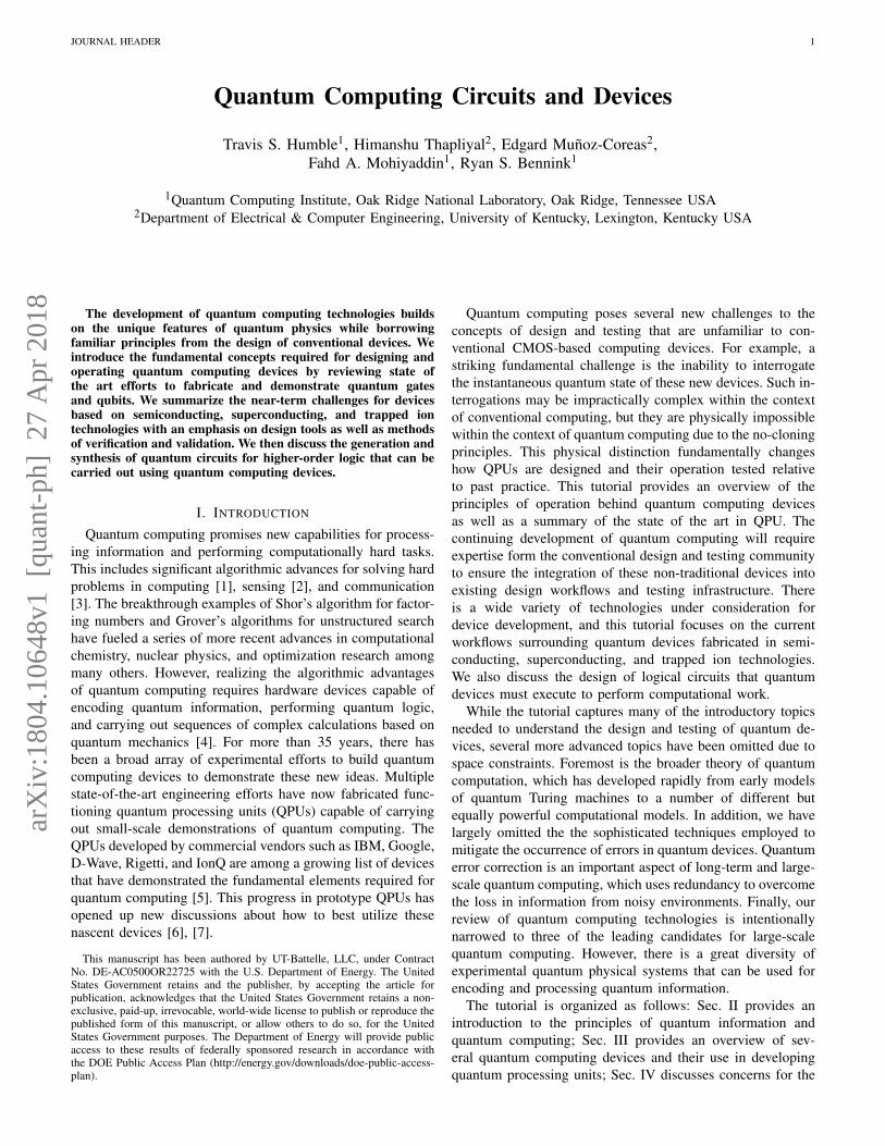
Fig. 1: The Bloch sphere with a unit radius provides a geo-metrical representation of a qubit. The north and south polesof the sphere define the orthonormal basis states |0〉 and |1〉,respectively, while the surface defines the set of all possiblequbit values. In spherical coordinates, the example qubit |Ψ〉has expansion coefficients c0 = cos θ and c1 = eiφ sin θ.
A prominent example of a quantum state within the contextof quantum computing is the case of a qubit. A qubit, orquantum bit, refers to the quantum state of an isolated two-level quantum mechanical system. Informally, the qubit is thequantum analog of bit. A qubit is the fundamental unit ofinformation within quantum computing. In the developmentof quantum computing technologies, a qubit is stored within aphysical two-level system. We denote those physical systemsas quantum register elements, in which an individual quantumregister element represents the ability to store a single qubitof information. We will discuss some of the different physicalsystems as quantum register elements in Sec. III. Logically,the qubit is defined over a basis of binary states labeled as‘0’ and ‘1’, respectively, such that an arbitrary state of a qubitmay be expressed as the linear combination
|ψ〉 = c0|0〉+ c1|1〉 (3)
The superposition of orthogonal basis states is fundamentalto quantum mechanics. Recall that the expansion coefficientsare complex-valued numbers normalized as |c0|2 + |c1|2 = 1.As the absolute phase of a quantum state is arbitrary [8], aconvenient graphical representation of the qubit is given inspherical coordinates. As shown in Fig. 1, the surface of aunit sphere represents all possible qubit values, where thepoints of |0〉 and |1〉 are located at the north and south poles,respectively. An arbitrary quantum state |Ψ〉 is normalized tounity and must lie on the surface of the sphere. In Fig. 1, theamplitudes c0 and c1 represent the projection of the quantumstate onto the corresponding basis states and the example qubit|Ψ〉 has expansion coefficients c0 = cos θ and c1 = eiφ sin θ.This representation of the qubit state on a unit sphere iscommonly called the Bloch sphere in quantum mechanics.
A multi-qubit register is an addressable array of n two-level physical systems. The principle of superposition may be
JOURNAL HEADER 3
extended to the register as the quantum state for the compositephysical system is also given by Eq. (1). For an n-qubitregister, the computational basis is expressed in binary notationas
|j〉 = |j1, j2, . . . , jn〉 = |j1〉 ⊗ |j2〉 . . .⊗ |jn〉, (4)
where the binary values jk correspond to the binary expansionof j. The dimensionality of the underlying Hilbert space isN = 2n and any normalized vector represents a valid quantumstate. In particular, there are composite quantum states whichcannot be expressed as separable products of n single-qubitstates. Such states are known as entangled states and theyare a hallmark of quantum mechanics and, therefore, quantumcomputing. For example, consider the quantum state of a 2-qubit register
|Ψ〉 =1√2
(|0, 0〉+ |1, 1〉) . (5)
Measuring the individual elements of the register will generatebinary outcomes 0 or 1 with equal probability. Accordingly,the classical expectation for a joint measurement of the registeris a uniform distribution of four possible outcomes. However,measurements of this quantum state are always correlatedsuch that both results are either (0,0) or (1,1), where theprobability for each of these outcomes is 1/2. Notably, thereis no possibility for observing anti-correlated outcomes forthis quantum state, e.g., (0, 1). The presence of these correla-tions in the measurement statistics is known as entanglementand the underlying quantum state is said to be entangled.Fundamentally, entanglement is a limitation on the ability todescribe states of a register solely by specifying the valueof each register element, and entangled states are notable forthe ability to violate the local, causal relations predicted byclassical mechanics [10].
The no-cloning principle represents a fundamental con-straint placed on quantum information processing. The no-cloning principle is a consequence of the linearity of quantummechanics [11], in which the ability to perfectly clone, akacopy, an arbitrary quantum state is not permitted. In particular,given a quantum register storing an arbitrary state |Ψ1〉, thisinformation cannot be copied into a second register withoutloss of information. Efforts to optimally approximate the valueof the first register, known as quantum cloning [12], can beevaluated by measuring the fidelity defined
f = | 〈Ψ2|Ψ1〉 |2, (6)
where |Ψ2〉 is the value of the second register and f ∈ [0, 1].The principles of operation for a quantum computer are
based on the Schrodinger’s equation in Eq. (2), in which thetime-dependent Hamiltonian H(t) can be directly controlledthrough the use of externally applied fields. Depending onthe specific technology in place, these controls will consistof electrical, magnetic, or optical fields designed to drive thedynamics toward a specific response. In Sec. III, we presentexamples for devices based on semiconductors, superconduc-tors, and trapped ion technologies. In some computationalmodels, the time-dependent controls are realized as pulsedfields that act discretely on the quantum register elements.
These discrete periods of field interaction are known as gatesand the effect of the gate on the quantum register is describedby an unitary operator that transforms the stored quantumstate. This is known as the gate or circuit model since adiagrammatic sequence of gates acting on registers provides adesign for instruction execution.
An alternative computational model applies the time-dependent field as continuous interaction subject to constraintson the rate of change for the overall Hamiltonian. This con-straint imposes an adiabatic condition on the dynamics of thequantum system [13], such that the Hamiltonian slowly mod-ifies the interactions between quantum physical subsystems,i.e., register elements, relative to the internal energy scalesdescribing those subsystems. As a result, the register state canbe driven toward a desired outcome. This is known as theadiabatic model given the constraints on the controls. A devicedesign based on the adiabatic model has been implementedin superconducting technology by the commercial vendor D-Wave Systems, Inc. In the realization of that design, theHamiltonian control is restricted to a specific functional form,namely the transverse Ising model, which limits the deviceoperation to computing discrete optimization problems. Inaddition, the physics of the device are not well modeled bythe Schrodinger equation, cf. Eq. (2), but rather require a moresophisticated model that includes non-trivial interactions withthe surrounding quantum physical systems as well as finitetemperature effects [14]. Nonetheless, the device has beenobserved to correctly compute the solution to a wide variety ofdiscrete optimization problems and has been characterized ashaving some advantages relative to conventional computingdevices. While the remainder of this tutorial will focus onthe gate model for quantum computing, we refer the readerinterested in adiabatic quantum computing to the recent reviewby Albash and Lidar [15].
We now summarize the basic criteria that define theexpected functionality of quantum computing devices. Asfirst presented by DiVincenzo [16], these criteria representthe minimal behaviors needed to perform general-purposequantum computing in the presence of likely architecturalconstraints. First is the ability to address the elements ina scalable register of quantum systems. Scalability impliesa manufacturing capability to fabricate and layout as manyregister elements as needed for a specific computation. Second,these register elements must be capable of being initializedwith high fidelity, as the starting quantum state of the compu-tation must be well-known to ensure accurate results. The thirdcriterion is the ability to measure register elements in a well-specified basis. As discussed above, measurement samples thestatistical distribution encoded by the quantum state accordingthe probabilities pi over a given basis set. A measurementsample represents readout from the register of the quantumcomputer and this value may be subsequently processed.
Fourth, the control over the register must include the abilityto apply sequences of gates drawn from a universal set. Uni-versality of the gate set characterizes the potential to performan arbitrary unitary operation on the quantum state using asufficiently long series of gates from that set. In particular, itis known that a finite set of gates is sufficient to approximate
JOURNAL HEADER 4
universality and, moreover, that a finite set of addressable one-and two-qubit gates are sufficient for universality [17]. Thelatter result, known as the Solovay-Kitaev theorem, providesa constructive method for composing arbitrary gates from afinite, universal gate set. Selection of a universal gate set raisesthe question of the optimal instruction set architecture for anintended application within a specific device technology [18].The fifth criterion is that the gate operation times must bemuch shorter than the characteristic interaction times on whichthe register couples to other unintended quantum physicalsystems. These interactions induce decoherence of the storedquantum superposition states, which leads to the loss ofinformation [19], [20]. In order to maintain the stored quantumstate with sufficient accuracy, the duration of the gate sequencemust be shorter than the characteristic decoherence time. Fault-tolerant protocols for gate operations are designed to counterthe losses from decoherence and other errors by redundantlyencoding information with quantum error correction codes[21].
Two additional functional criteria are necessary for a quan-tum computer with geometrical constraints on the layout ofthe quantum register. In particular, layout constraints mayimpose restrictions on which register elements can be ad-dressed by multi-qubit gates, e.g., nearest neighbors withina two-dimensional rectangular lattice design. Physical layoutrestrictions may be overcome by moving stored quantum statesbetween register elements. This is accomplished using theSWAP gate, a unitary operation that exchanges the quantumstate between two register elements. In addition, a MOVEoperation can support long distance transport of a storedvalue, in which the register element itself is displaced. Thelatter proves useful for distributed quantum registers that mayrequires interconnects, aka communication buses, to SWAPregister values. The necessity of these functions depends onthe purpose of the quantum computer and especially thelimitations of the technology. Presently, all technologies forquantum computing face some constraints on register layout.
III. DEVICES FOR QUANTUM COMPUTING
There are many different possible technologies available forbuilding quantum computers, and these are typically classifiedby how qubits of information are stored. As discussed inSec. II, these devices must meet several functional criteria tocarry out reliable quantum computation. In this section, weprovide an overview of three technologies that are currentlyused for developing quantum computing devices and wediscuss the progress toward meeting the functional criteria.
A. Silicon Spin Qubits
Silicon spin qubits denote a technology implementationby which quantum information is encoded either in the spinstates of an electron found in a silicon quantum dot, or inthe spin state of the electron or nucleus of a single-dopantatom (typically group V donors) in a silicon substrate. Inparticular, the orientation of the spin in these systems is used toencode the |0〉 and |1〉 states. Notably, these silicon devices arefabricated with conventional CMOS techniques, and consist of
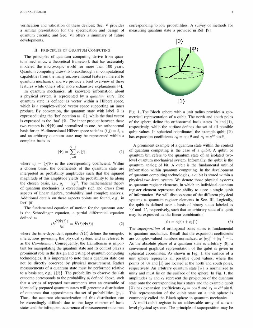
gate electrodes (normally Aluminum or Polysilicon) that cancontrol the energy landscape in the silicon substrate. Theseelectrodes are appropriately designed and biased such that asingle electron is confined in a quantum dot at the interface.Examples of a silicon quantum dot include the MOS deviceshown in Fig. 2(a) or the Si/SiGe device shown in Fig. 2(b).Similar electrostatic control is used for silicon donor deviceslike the example shown in Fig. 2(c) of a Phosphorus donorimplanted inside a silicon substrate. In all of these examples,the electrons are strongly confined such that lowest electronicorbital energy in the quantum dot or the donor is well isolatedfrom other excited electronic states. The confinement lengthfor the donor electron is ∼ 1.5 nm in all 3-dimensions, whilefor the dot electron, these dimensions are ∼ 10 nm and∼ 2 nm in the lateral and vertical directions, respectively.These characteristic dimensions make silicon qubits the mostcompactly fabricated technology as compared to the qubittechnologies discussed in later subsections.
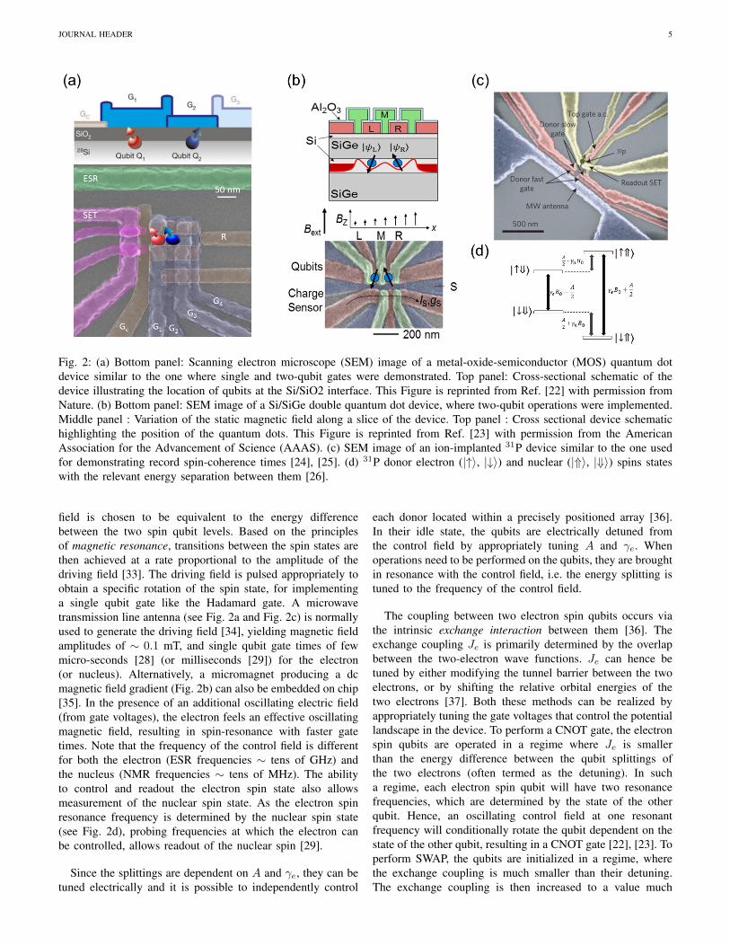
Addressing silicon spin qubits uses an applied static mag-netic field B0 to split the orbital degeneracy of the dot-electronat the interface. Due to the Zeeman effect, the orbital for theconfined electron is split into the distinct spin states |↑〉 and|↓〉. These spin states encode the computational states |0〉 and|1〉, where the energy splitting is given by the Zeeman energyγeB0 with γe ∼ 28 GHz/T the gyromagnetic ratio of theelectron. For 31P donors, the electron and nuclear spins arecoupled by the hyperfine interaction A ∼ 117 MHz [27]. Thedonor qubits are generally operated under large magnetic fieldsB0 > 1 T, such that (γe + γn)B0 � A, where γn ∼ 17MHz/T is the gyromagnetic ratio of the nucleus. In this limit,the eigen spin states are tensor products of the electronic spin(|↑〉, |↓〉) and the nuclear spin (|⇑〉, |⇓〉) states. The resultingenergies are shown in Fig. 2(d), where the electron spin qubitsplitting depends on the nuclear spin states, and vice versa.Typical energy splittings are of the order of tens of GHz andMHz for the electron and nuclear spins, respectively [28], [29].The hyperfine interaction A and the electron gyromagneticratio γe depend on the orbital wavefunction of the electron,which can be tuned with electric fields [30], [31]. As a result,the qubit splittings are electrically tunable after the siliconqubit devices are fabricated.
Electron spin qubits are commonly initialized and measuredusing spin-charge conversion techniques [32]. Charge sensorssuch as quantum point contacts and single-electron-transistors(SET) are located adjacent to the quantum dot (or donor) andare then capacitively coupled to them, cf. Fig. 2. The chargesensors are biased appropriately with gate voltages, such thatthe current passing through them is strongly sensitive to theelectrostatic environment in their vicinity. The orbital energyof the electron is then electrically tuned such that the electroncan preferentially tunnel to the same or another nearby chargereservoir, depending on its spin. The presence or absence ofthe electron on the donor/dot can then be detected via a changein current passing through the charge sensors, which aids toreadout the electron spin state. The protocol will also initializethe electron spin state in the dot or the donor to |↓〉 [32].
For spin control, an oscillating (driving) magnetic fieldis applied to the qubits. The frequency of the oscillating
JOURNAL HEADER 5
Fig. 2: (a) Bottom panel: Scanning electron microscope (SEM) image of a metal-oxide-semiconductor (MOS) quantum dotdevice similar to the one where single and two-qubit gates were demonstrated. Top panel: Cross-sectional schematic of thedevice illustrating the location of qubits at the Si/SiO2 interface. This Figure is reprinted from Ref. [22] with permission fromNature. (b) Bottom panel: SEM image of a Si/SiGe double quantum dot device, where two-qubit operations were implemented.Middle panel : Variation of the static magnetic field along a slice of the device. Top panel : Cross sectional device schematichighlighting the position of the quantum dots. This Figure is reprinted from Ref. [23] with permission from the AmericanAssociation for the Advancement of Science (AAAS). (c) SEM image of an ion-implanted 31P device similar to the one usedfor demonstrating record spin-coherence times [24], [25]. (d) 31P donor electron (|↑〉, |↓〉) and nuclear (|⇑〉, |⇓〉) spins stateswith the relevant energy separation between them [26].
field is chosen to be equivalent to the energy differencebetween the two spin qubit levels. Based on the principlesof magnetic resonance, transitions between the spin states arethen achieved at a rate proportional to the amplitude of thedriving field [33]. The driving field is pulsed appropriately toobtain a specific rotation of the spin state, for implementinga single qubit gate like the Hadamard gate. A microwavetransmission line antenna (see Fig. 2a and Fig. 2c) is normallyused to generate the driving field [34], yielding magnetic fieldamplitudes of ∼ 0.1 mT, and single qubit gate times of fewmicro-seconds [28] (or milliseconds [29]) for the electron(or nucleus). Alternatively, a micromagnet producing a dcmagnetic field gradient (Fig. 2b) can also be embedded on chip[35]. In the presence of an additional oscillating electric field(from gate voltages), the electron feels an effective oscillatingmagnetic field, resulting in spin-resonance with faster gatetimes. Note that the frequency of the control field is differentfor both the electron (ESR frequencies ∼ tens of GHz) andthe nucleus (NMR frequencies ∼ tens of MHz). The abilityto control and readout the electron spin state also allowsmeasurement of the nuclear spin state. As the electron spinresonance frequency is determined by the nuclear spin state(see Fig. 2d), probing frequencies at which the electron canbe controlled, allows readout of the nuclear spin [29].
Since the splittings are dependent on A and γe, they can betuned electrically and it is possible to independently control
each donor located within a precisely positioned array [36].In their idle state, the qubits are electrically detuned fromthe control field by appropriately tuning A and γe. Whenoperations need to be performed on the qubits, they are broughtin resonance with the control field, i.e. the energy splitting istuned to the frequency of the control field.
The coupling between two electron spin qubits occurs viathe intrinsic exchange interaction between them [36]. Theexchange coupling Je is primarily determined by the overlapbetween the two-electron wave functions. Je can hence betuned by either modifying the tunnel barrier between the twoelectrons, or by shifting the relative orbital energies of thetwo electrons [37]. Both these methods can be realized byappropriately tuning the gate voltages that control the potentiallandscape in the device. To perform a CNOT gate, the electronspin qubits are operated in a regime where Je is smallerthan the energy difference between the qubit splittings ofthe two electrons (often termed as the detuning). In sucha regime, each electron spin qubit will have two resonancefrequencies, which are determined by the state of the otherqubit. Hence, an oscillating control field at one resonantfrequency will conditionally rotate the qubit dependent on thestate of the other qubit, resulting in a CNOT gate [22], [23]. Toperform SWAP, the qubits are initialized in a regime, wherethe exchange coupling is much smaller than their detuning.The exchange coupling is then increased to a value much
JOURNAL HEADER 6
larger than their detuning, such that the two qubits exchangeinformation with each other. After an appropriate time thatdetermines the angle of SWAP, the exchange coupling isbrought back to a low value.
The spin-orbit coupling is weak for electrons in silicon,resulting in long spin-relaxation times T1. The relaxation timehas been shown to be dependent on the temperature and mag-netic field [38]. Operating the qubits at low temperatures (<1 K) and magnetic fields (< 5 T), yield T1 exceeding severalseconds and even hours. The presence of spin containingnuclei (such as Si-29) in the lattice, and their fluctuations,can result in decoherence of the electron spins [39]. Hence,isotopic purification of silicon from spin containing nuclei,allows for long-coherence times (T2) of milli-seconds andseconds for the electron and nuclear spins respectively [25].Additional sources of decoherence include charge or electricfield noise arising from nearby defects/traps, control signals,gate electrodes and thermal radiation from the microwaveantenna [25].
While the methods to address and couple silicon qubits canbe integrated with the microelectronics industry, the qubitsare very sensitive to atomic details that have not yet beenaddressed in the industry. These details strongly affect thequbit operation, and hence it is essential to design devices thatminimizes their influence on the qubits. First, the exchangecoupling between donor electrons is extremely sensitive tothe position of donors, necessitating precise donor placementaccuracies and/or large exchange coupling tunabilities [40],[41]. Efforts are underway to demonstrate qubits with single-donor atoms in silicon that are placed precisely with ScanningTunneling Microscopy [42], as well as to explore alternatemeans of coupling between the qubits (such as dipolar inter-actions [43], [44]) that are less sensitive to donor placementinaccuracies. In addition, atomic roughness and step edges atthe interface, can result in the excited orbital states comingclose to the ground orbital state in silicon quantum dots,accelerating relaxation and even resulting in a non spin-1/2ground states [38]. The energy separation between the groundand excited orbital states (also referred to as valley splitting)can be tuned with electric field to an extent [45], yet it isalways desirable to obtain larger and uniform valley splittingswith a smooth interface. Finally, uncontrolled strain in thelattice arises from the thermal mismatch between the gateand substrate materials when the device is cooled from roomtemperature to milli-Kelvin temperatures [46]. This modifiesthe potential landscape in the device, altering the positionand confinement of the quantum dots, along with introducingaccidental dots. Ref. [46] highlights that using gate materials(such as polysilicon rather than aluminum) which have similarthermal expansion coefficients to that of silicon, can aid toreduce the lattice strain.
The exchange interaction between the qubits is short-range(within few tens of nm), and can only result in nearest-neighbor couplings. To scale up silicon qubit devices to alarge-scale architecture, it is beneficial to have connectivitybetween qubits that are separated by much larger distances.Methods to couple silicon qubits to a photonic mode spanning∼ centimeter in a microwave resonator have been proposed
previously [43], [47], and recently demonstrated in Si/SiGequantum dots [48], [49]. Through the photonic mode, twoqubits separated by as far a centimeter can be virtually coupledto each other, enhancing the qubit-connectivity significantly.Coupling the spins to the resonator also provides a pathway toreadout the spin states [43]. The transmission frequency of theresonator then depends on the spin state of the qubit. Hence,applying a microwave signal to the resonator, and measuringits transmission aids to detect the spin state.
Designing silicon spin qubit devices requires modelingseveral classical and quantum mechanical parameters with arange of techniques that are adapted from the semiconductorindustry [26]. Classical variables that are relevant and needto be solved for include the electrostatic potential landscape,electric fields, electron densities, capacitances, magnetic fieldsand strain. The electrostatic parameters in silicon devices canbe obtained by solving Poisson’s equation with the finite-element method with traditional TCAD design packages suchas Sentaurus TCAD, or a general multiphysics package likeCOMSOL. Solving Maxwell’s equations with high-frequencyelectromagnetic solvers (such as CST-Microwave Studio orANSYS-HFSS) aids to estimate the driving magnetic fieldsgenerated by the microwave antenna in such devices. Thermalstrain while cooling such devices can also be simulated bysolving the stress-strain equations with COMSOL [46]. Inaddition to the classical parameters, it is also essential to solvethe electronic structure in silicon qubit devices, and estimatethe electron orbital-energies, and wave functions. Effectivemass theory and tight-binding techniques have been exten-sively used for such calculations [38]. The orbital energiesand wave functions act as a handle to the hyperfine, exchangeand tunnel couplings, along with the electron gyromagneticratio and electron spin relaxation times. These parametersare ultimately fed into a simplified spin Hamiltonian, whichis solved with mathematical packages (such as MATLAB,Mathematica or QuTiP), to simulate the instantaneous spinstates and quantum gate fidelities.
B. Trapped Ion Qubits
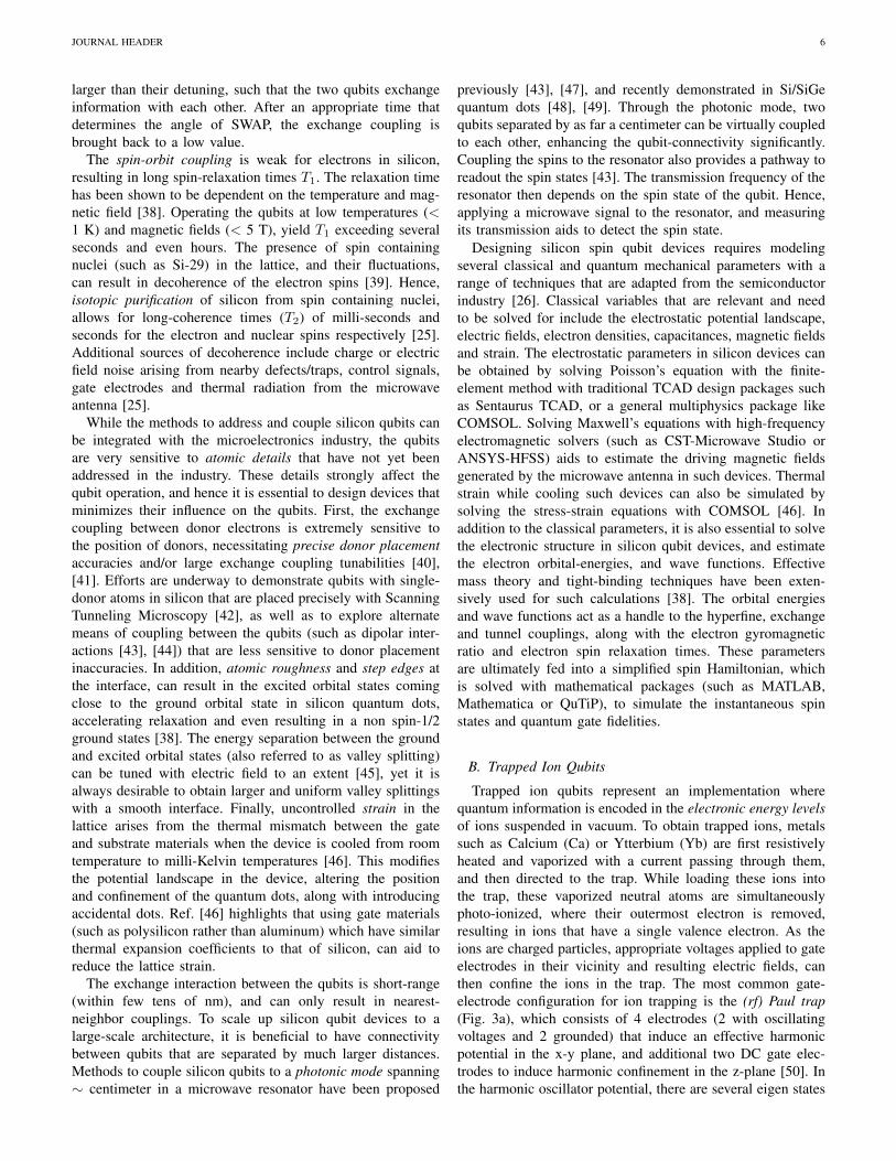
Trapped ion qubits represent an implementation wherequantum information is encoded in the electronic energy levelsof ions suspended in vacuum. To obtain trapped ions, metalssuch as Calcium (Ca) or Ytterbium (Yb) are first resistivelyheated and vaporized with a current passing through them,and then directed to the trap. While loading these ions intothe trap, these vaporized neutral atoms are simultaneouslyphoto-ionized, where their outermost electron is removed,resulting in ions that have a single valence electron. As theions are charged particles, appropriate voltages applied to gateelectrodes in their vicinity and resulting electric fields, canthen confine the ions in the trap. The most common gate-electrode configuration for ion trapping is the (rf) Paul trap(Fig. 3a), which consists of 4 electrodes (2 with oscillatingvoltages and 2 grounded) that induce an effective harmonicpotential in the x-y plane, and additional two DC gate elec-trodes to induce harmonic confinement in the z-plane [50]. Inthe harmonic oscillator potential, there are several eigen states
JOURNAL HEADER 7
corresponding to the vibrational modes of the trapped ions.To ensure that thermal effects and fluctuating electromagneticfields do not cause random excitation of these states andthereby motion of the ions, the ions are laser-cooled to theirvibrational ground state [51]. For a small number of ions(∼ 50), the ions will then be arranged in a linear chain alongthe z-direction, such that overall forces from the external fieldscancel out the forces from their Coulomb interaction. Typicalion separation in the trap is ∼ 10 µm.
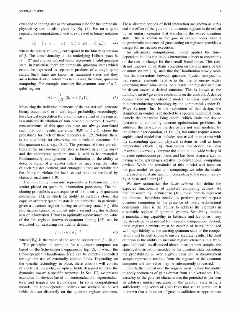
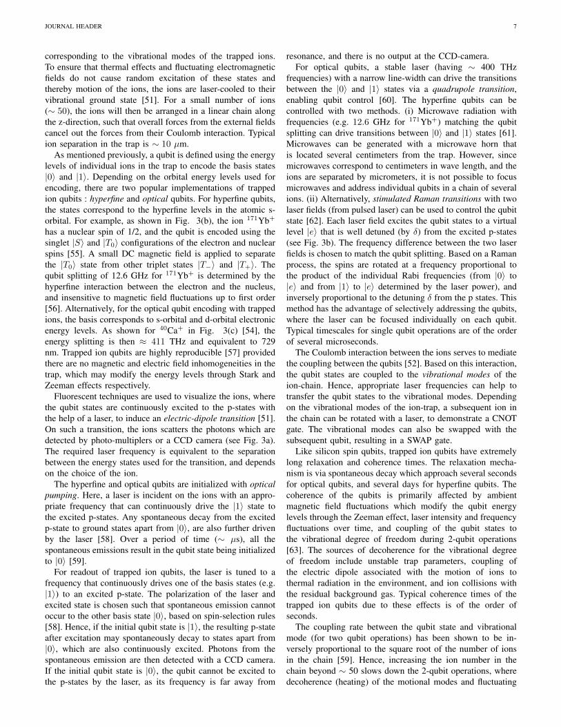
As mentioned previously, a qubit is defined using the energylevels of individual ions in the trap to encode the basis states|0〉 and |1〉. Depending on the orbital energy levels used forencoding, there are two popular implementations of trappedion qubits : hyperfine and optical qubits. For hyperfine qubits,the states correspond to the hyperfine levels in the atomic s-orbital. For example, as shown in Fig. 3(b), the ion 171Yb+
has a nuclear spin of 1/2, and the qubit is encoded using thesinglet |S〉 and |T0〉 configurations of the electron and nuclearspins [55]. A small DC magnetic field is applied to separatethe |T0〉 state from other triplet states |T−〉 and |T+〉. Thequbit splitting of 12.6 GHz for 171Yb+ is determined by thehyperfine interaction between the electron and the nucleus,and insensitive to magnetic field fluctuations up to first order[56]. Alternatively, for the optical qubit encoding with trappedions, the basis corresponds to s-orbital and d-orbital electronicenergy levels. As shown for 40Ca+ in Fig. 3(c) [54], theenergy splitting is then ≈ 411 THz and equivalent to 729nm. Trapped ion qubits are highly reproducible [57] providedthere are no magnetic and electric field inhomogeneities in thetrap, which may modify the energy levels through Stark andZeeman effects respectively.
Fluorescent techniques are used to visualize the ions, wherethe qubit states are continuously excited to the p-states withthe help of a laser, to induce an electric-dipole transition [51].On such a transition, the ions scatters the photons which aredetected by photo-multiplers or a CCD camera (see Fig. 3a).The required laser frequency is equivalent to the separationbetween the energy states used for the transition, and dependson the choice of the ion.
The hyperfine and optical qubits are initialized with opticalpumping. Here, a laser is incident on the ions with an appro-priate frequency that can continuously drive the |1〉 state tothe excited p-states. Any spontaneous decay from the excitedp-state to ground states apart from |0〉, are also further drivenby the laser [58]. Over a period of time (∼ µs), all thespontaneous emissions result in the qubit state being initializedto |0〉 [59].
For readout of trapped ion qubits, the laser is tuned to afrequency that continuously drives one of the basis states (e.g.|1〉) to an excited p-state. The polarization of the laser andexcited state is chosen such that spontaneous emission cannotoccur to the other basis state |0〉, based on spin-selection rules[58]. Hence, if the initial qubit state is |1〉, the resulting p-stateafter excitation may spontaneously decay to states apart from|0〉, which are also continuously excited. Photons from thespontaneous emission are then detected with a CCD camera.If the initial qubit state is |0〉, the qubit cannot be excited tothe p-states by the laser, as its frequency is far away from
resonance, and there is no output at the CCD-camera.For optical qubits, a stable laser (having ∼ 400 THz
frequencies) with a narrow line-width can drive the transitionsbetween the |0〉 and |1〉 states via a quadrupole transition,enabling qubit control [60]. The hyperfine qubits can becontrolled with two methods. (i) Microwave radiation withfrequencies (e.g. 12.6 GHz for 171Yb+) matching the qubitsplitting can drive transitions between |0〉 and |1〉 states [61].Microwaves can be generated with a microwave horn thatis located several centimeters from the trap. However, sincemicrowaves correspond to centimeters in wave length, and theions are separated by micrometers, it is not possible to focusmicrowaves and address individual qubits in a chain of severalions. (ii) Alternatively, stimulated Raman transitions with twolaser fields (from pulsed laser) can be used to control the qubitstate [62]. Each laser field excites the qubit states to a virtuallevel |e〉 that is well detuned (by δ) from the excited p-states(see Fig. 3b). The frequency difference between the two laserfields is chosen to match the qubit splitting. Based on a Ramanprocess, the spins are rotated at a frequency proportional tothe product of the individual Rabi frequencies (from |0〉 to|e〉 and from |1〉 to |e〉 determined by the laser power), andinversely proportional to the detuning δ from the p states. Thismethod has the advantage of selectively addressing the qubits,where the laser can be focused individually on each qubit.Typical timescales for single qubit operations are of the orderof several microseconds.
The Coulomb interaction between the ions serves to mediatethe coupling between the qubits [52]. Based on this interaction,the qubit states are coupled to the vibrational modes of theion-chain. Hence, appropriate laser frequencies can help totransfer the qubit states to the vibrational modes. Dependingon the vibrational modes of the ion-trap, a subsequent ion inthe chain can be rotated with a laser, to demonstrate a CNOTgate. The vibrational modes can also be swapped with thesubsequent qubit, resulting in a SWAP gate.
Like silicon spin qubits, trapped ion qubits have extremelylong relaxation and coherence times. The relaxation mecha-nism is via spontaneous decay which approach several secondsfor optical qubits, and several days for hyperfine qubits. Thecoherence of the qubits is primarily affected by ambientmagnetic field fluctuations which modify the qubit energylevels through the Zeeman effect, laser intensity and frequencyfluctuations over time, and coupling of the qubit states tothe vibrational degree of freedom during 2-qubit operations[63]. The sources of decoherence for the vibrational degreeof freedom include unstable trap parameters, coupling ofthe electric dipole associated with the motion of ions tothermal radiation in the environment, and ion collisions withthe residual background gas. Typical coherence times of thetrapped ion qubits due to these effects is of the order ofseconds.
The coupling rate between the qubit state and vibrationalmode (for two qubit operations) has been shown to be in-versely proportional to the square root of the number of ionsin the chain [59]. Hence, increasing the ion number in thechain beyond ∼ 50 slows down the 2-qubit operations, wheredecoherence (heating) of the motional modes and fluctuating
JOURNAL HEADER 8
Fig. 3: (a) Schematic of a Paul trap used to confine ions in vacuum. Inset : Visualization of ions in the trap with fluorescenttechniques. This Figure is reprinted from Ref. [52] with permission from Nature. (b) Electronic energy levels of a 171Yb+
ion illustrating qubit encoding (|0〉 and |1〉) with hyperfine energy levels [53]. Transition between qubit states is achieved bya Raman process via excitation to a virtual state |e〉. (c) Electronic energy levels of a 40Ca+ ion illustrating qubit encodingwith the s- and d-orbital energy levels. This Figure is reprinted from Ref. [54] with permission from Springer.
electric fields become significant. Architectures for scale upwith larger number of ions include Quantum Charge CoupledDevice (QCCD) architectures [64] where individual ions at theedges of a trap are shuttled to nearby traps and made to interactwith them, for connecting distant qubits. This would requireexquisite control of the shuttling of the atomic ions, as wellas the periodically cooling down the excess motion arisingfrom shuttling ions. While this method could potentially workfor larger number of qubits (∼ 1000), it becomes impracticalfor scale-up due to complexity of interconnects, diffraction ofoptical beams, and extensive hardware requirements. Photonicinterfaces have been proposed to connect even larger systems[59]. Here, qubits at the edges of the chain are driven to anexcited state with very fast laser pulses so that at most one pho-ton emerges from each qubit after radiative decay. Followingselection rules, the radiative decay can lead to entanglementbetween the photonic and trapped ion qubit. Photons from twoseparate qubits are mode-matched and interfered on a beam-splitter, which is then detected. A successful detection thenyields an entangled state between the two distant ion trapqubits.
The design packages available in the conventional micro-electronics industry cannot be directly extended to designtrapped ion qubits, as their implementation has very littleoverlap with that of silicon. Nevertheless, the electric fieldsavailable from classical electrostatic solvers (such as COM-SOL) can be used to optimize and design the gate electrodeconfiguration and voltages for the trap. As illustrated previ-ously in this section, the electronic orbital levels of singleions (or even a cluster of ions) in the trap, determine thelaser frequencies needed for initialization, readout, control andcoupling of the trapped ion qubits. The orbital energies andhyperfine interactions for a variety of trapped ion candidatematerials can be determined from ab-initio electronic struc-ture calculation techniques such as density functional theory(DFT). A significant aspect of the design also include theoptical setup for the lasers, including its power and focus.
These parameters can be obtained with commercial ray-tracingsoftware packages such as Zemax, Code V or Oslo. Thedynamics of the trapped ion qubits upon interaction with alaser can be mapped onto a simplified Hamiltonian, which canthen be solved with commercial mathematical packages, suchas MATLAB. While there are several analytical expressionsand mathematical models for light-matter interactions, a devicesimulator capable of capturing the non-idealities in realistictrapped ion devices is currently non-existent.
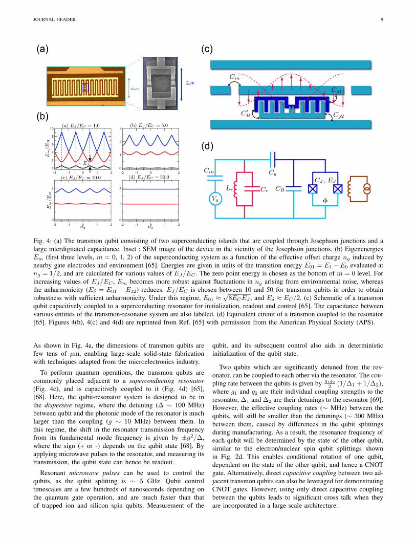
C. Superconducting Transmon Qubits
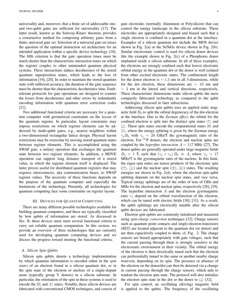
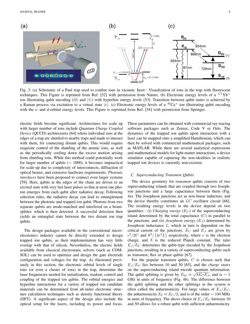
The device geometry for transmon qubits consists of twosuperconducting islands that are coupled through two Joseph-son junctions and a large capacitance between them (Fig.4a). The Josephson junctions act as non-linear inductors, andthe device thereby constitutes an LC oscillator circuit [66].The resulting energy levels in the device depend on twoquantities : (i) Charging energy (EC) of the superconductingisland determined by the total capacitance (C) in parallel tothe junctions, and (ii) Josephson energy (EJ ) determined byJosephson inductance L, which in turn is dependent on thecritical current of the junctions. EC and EJ are given bye2/2C and ~2/
(4e2L
)respectively, where e is the electron
charge, and ~ is the reduced Planck constant. The ratioEJ/EC determines the qubit-type encoded by the Jospehsonjunctions, resulting in a variety of superconducting qubits suchas transmon, flux or phase qubits [67].
For the popular transmon qubits, C is chosen such thatEJ/EC lies between 10 and 50 [65], and the charge stateson the superconducting island encode quantum information.The qubit splitting is given by E01 ≈
√8ECEJ , and is ∼ 5
GHz in units of frequency (Fig. 4b). The difference betweenthe qubit splitting and the other splittings in the system isoften called the anharmonicity. For large values of EJ/EC ,the anharmonicity Eδ ≈ EC/2, and is of the order ∼ 100 MHzin units of frequency. The above choice of EJ/EC between 10and 50 allows for a robust qubit with sufficient anharmonicity.
JOURNAL HEADER 9
Fig. 4: (a) The transmon qubit consisting of two superconducting islands that are coupled through Josephson junctions and alarge interdigitated capacitance. Inset : SEM image of the device in the vicinity of the Josephson junctions. (b) EigenenergiesEm (first three levels, m = 0, 1, 2) of the superconducting system as a function of the effective offset charge ng induced bynearby gate electrodes and environment [65]. Energies are given in units of the transition energy E01 = E1 −E0 evaluated atng = 1/2, and are calculated for various values of EJ/EC . The zero point energy is chosen as the bottom of m = 0 level. Forincreasing values of EJ/EC , Em becomes more robust against fluctuations in ng arising from environmental noise, whereasthe anharmonicity (Eδ = E01 − E12) reduces. EJ/EC is chosen between 10 and 50 for transmon qubits in order to obtainrobustness with sufficient anharmonicity. Under this regime, E01 ≈
√8ECEJ , and Eδ ≈ EC/2. (c) Schematic of a transmon
qubit capacitively coupled to a superconducting resonator for initialization, readout and control [65]. The capacitance betweenvarious entities of the transmon-resonator system are also labeled. (d) Equivalent circuit of a transmon coupled to the resonator[65]. Figures 4(b), 4(c) and 4(d) are reprinted from Ref. [65] with permission from the American Physical Society (APS).
As shown in Fig. 4a, the dimensions of transmon qubits arefew tens of µm, enabling large-scale solid-state fabricationwith techniques adapted from the microelectronics industry.
To perform quantum operations, the transmon qubits arecommonly placed adjacent to a superconducting resonator(Fig. 4c), and is capacitively coupled to it (Fig. 4d) [65],[68]. Here, the qubit-resonator system is designed to be inthe dispersive regime, where the detuning (∆ ∼ 100 MHz)between qubit and the photonic mode of the resonator is muchlarger than the coupling (g ∼ 10 MHz) between them. Inthis regime, the shift in the resonator transmission frequencyfrom its fundamental mode frequency is given by ±g2/∆,where the sign (+ or -) depends on the qubit state [68]. Byapplying microwave pulses to the resonator, and measuring itstransmission, the qubit state can hence be readout.
Resonant microwave pulses can be used to control thequbits, as the qubit splitting is ∼ 5 GHz. Qubit controltimescales are a few hundreds of nanoseconds depending onthe quantum gate operation, and are much faster than thatof trapped ion and silicon spin qubits. Measurement of the
qubit, and its subsequent control also aids in deterministicinitialization of the qubit state.
Two qubits which are significantly detuned from the res-onator, can be coupled to each other via the resonator. The cou-pling rate between the qubits is given by g1g2
2 (1/∆1 + 1/∆2),where g1 and g2 are their individual coupling strengths to theresonator, ∆1 and ∆2 are their detunings to the resonator [69].However, the effective coupling rates (∼ MHz) between thequbits, will still be smaller than the detunings (∼ 300 MHz)between them, caused by differences in the qubit splittingsduring manufacturing. As a result, the resonance frequency ofeach qubit will be determined by the state of the other qubit,similar to the electron/nuclear spin qubit splittings shownin Fig. 2d. This enables conditional rotation of one qubit,dependent on the state of the other qubit, and hence a CNOTgate. Alternatively, direct capacitive coupling between two ad-jacent transmon qubits can also be leveraged for demonstratingCNOT gates. However, using only direct capacitive couplingbetween the qubits leads to significant cross talk when theyare incorporated in a large-scale architecture.
JOURNAL HEADER 10
Compared to silicon and trapped-ion qubits, the relaxationand coherence times of superconducting qubits are short. Themain sources of decoherence arise from coupling of the qubitsto additional two level systems present in the bulk/interfacesof the device, non-equilibrium quasi-particles generated fromstray-infrared light, and radiation to additional modes presentin device [70], [71]. The relaxation rate has also been shownto be exponentially dependent on the temperature, due tothe qubit interaction with thermal photons [65]. As a result,extremely low temperatures ∼ 20 mK are necessary forhigh-fidelity operation of qubits. Different device designs andoperation regimes during the last decade have resulted inimprovements in the relaxation and coherence times by severalorders of magnitude. Dephasing times currently is of the orderof ∼ 100 µs.
The Josephson energy is strongly determined by the criticalcurrent across the junction, which in turn is dependent on thesuperconducting energy gap and the normal resistance (Rn) ofthe Josephson junction when it is operated above the criticaltemperature [72]. Rn is determined by the thickness (few nm)of the Josephson junction, and can be variable across differentdevices. This results in non-uniform qubit splittings acrossdevices, with an in-homogeneity of ∼ 300 MHz. Anothersignificant challenge is the large size (several tens of µm) ofsuperconducting qubits, limiting the number of qubits that canbe coupled to each other via a single resonator, which spansabout a centimeter. Scaling up current demonstrations to alarge-scale architecture with millions of well-connected qubitsoperating at extremely low temperature will benefit stronglyby a reduction in the size of the qubits [73].
While a standalone tool for designing superconductingqubits is non-existent, parameters such as the capacitance(for determining EC) and inductance (for determining EJ )can be estimated with classical electrostatic and electromag-netic packages such as FastCap and FastHenry respectively.Microwave software such as TXLINE (in AWR MicrowaveOffice) has been used to design and estimate the characteristicimpedance of the superconducting resonator, that aids toreadout, control and couple the qubits. In addition, the elec-tromagnetic fields experienced by the superconducting qubits,can be obtained by solving the Maxwell’s Equations with high-frequency electromagnetic simulators such as ANSYS-HFSS.As for silicon and trapped-ion qubits, the qubit dynamics canalso be obtained by solving the simplified Hamiltonian withmathematical packages.
IV. VERIFICATION AND VALIDATION OF QUANTUMDEVICES
In spite of the great progress in fabrication and controlof qubits, today’s quantum computing devices are far noisierand error-prone than conventional digital circuits. Bit errorprobabilities of 10−3 − 10−2 per qubit per operation (or perclock cycle) are typical. Even with continued progress in qubittechnologies, it is unlikely that the errors incurred by phys-ical qubits will ever become negligible. Thus understandingand mitigating fault processes in qubit devices is a criticalaspect of quantum computer development. Correspondingly,
the experimental testing of qubit devices primarily concernsthe accuracy and reliability of hardware operation rather thanthe correctness of the circuit logic. Experimental testing isessential here: since qubit devices are designed to performcomputations that would otherwise be impractical or impos-sible, realistic simulation at the device scale is not a viableoption.
Qubit device testing may be divided into two broad cate-gories: characterization, wherein the goal is to obtain a detailedmodel of a device’s fault modes; and benchmarking, whereinthe goal is to determine a few high-level performance metrics.Characterization is the more costly type of testing but canprovide important insights leading to fault mitigation strategiesor improved devices. For simply assessing the performance ofa device, benchmarking is more practical.
a) Benchmarking: Metrics and Techniques: The mostbasic performance metric is the probability that the deviceoutputs the correct state. In the context of quantum mechanics,this corresponds to the inner product (or “overlap”) betweenthe output state and the intended state, which is called the fi-delity. The infidelity, defined as 1 minus the fidelity, quantifiesthe amount of error in the output state. Another common wayof quantifying the output error is in terms of the geometricdistance between the output state and the target state in thecomplex vector space.
If a qubit device is used to output a specific quantum state,e.g. some reference state or resource state, the fidelity of theoutput with respect to this known state can be estimated bymeasuring random subsets of qubits along various directionsof the Bloch sphere [74], [75]. In such cases, the experimentalcost scales favorably with the register size. However, a qubitdevice would be used to perform a wide variety of compu-tations each with a different output state, and these outputstates presumably cannot be computed by any conventionalmeans. In this case one desires experimental metrics thatallow one to estimate or bound the fidelity of the deviceoutput for any computation it performs. The state-of-the-artapproach for this purpose is Randomized Benchmarking [76](RB). RB is a technique for assessing how much, on average,each operation decreases the output fidelity. Essentially, RBinvolves measuring the final fidelity of a qubit for randomoperation sequences of varying lengths. For weak uncorrelatederrors, the fidelity decays exponentially as a function ofsequence length. The RB decay constant is broadly interpretedas the average error per gate, an obviously useful performancemetric. Extensions of RB have been devised to yield operation-specific error metrics [77], [78], to incorporate multi-qubitoperations [79], to include qubit loss [80], and to assess crosstalk [81]. While RB remains a very popular benchmarkingmethod, its underlying fault model is not universal; hence RBin its current form may not be enitrely valid or accurate asengineering efforts continue to make the simple fault modesassumed by RB less and less prominent [82]. Additionally, ithas been noted that relating RB decay constants to operationfidelities is subtly problematic [83].
b) Characterization via Quantum Tomography: An al-ternative to benchmarking is to thoroughly characterize thefault modes of the device. Since the output state of a quan-
JOURNAL HEADER 11
tum circuit is exponentially large in the number of qubits,characterization of a quantum circuit as a whole is generallyinfeasible. The established strategy is to characterize eachoperation of a qubit device as completely as possible, sothat the result of any given sequence of operations can (inprinciple) be predicted accurately. The general name for thisstrategy is quantum tomography, a name derived from themedical imaging technique in which a 3-dimensional image ofa subject is reconstructed from a set of 2-dimensional projec-tions. In a similar manner, quantum tomography reconstructsa quantum state or operation from multiple measurements,each of which reveals a particular projection of the state. Thisreconstruction is based on the fact that a quantum state isuniquely specified by the probability distributions for certaincharacteristic quantities of a physical system. (For a spin qubit,the characteristic quantities are the projection of the spin alongthree independent spatial directions.) State tomography is thedetermination of the quantum state via statistical estimationof these characteristic distributions. Tomographic methodscan also be used to characterize qubit operations. A qubitoperation can be thought of as a linear transformation ofthe characteristic probability distributions. Quantum processtomography is the determination of the transformation matrixby characterizing the output state for each possible input state,or more precisely, for a set of linearly independent states thatspan the state space.
Quantum tomography as just described requires well-calibrated measurements, whereas qubit measurements areamong the device operations that need to be characterized.This problem is overcome with Gate Set Tomography [84],[85], the state-of-the-art method for detailed characterizationof qubit devices. Gate set tomography involves tomographicmeasurements of many different sequences of device opera-tions. These sequences, which range in length up to hundredsor thousands of operations, are carefully chosen to reveal allpossible types of qubit errors. The data is then fit to a highlynonlinear model using a sophisticated procedure, yielding aself-consistent model of all of a device’s operations, includingthe measurement operations themselves. Gate Set Tomographyhas been used to characterize and significantly improve thecontrol of trapped ion qubits [86].
c) Other Approaches: In addition to Randomized Bench-marking and Gate Set Tomography, a number of other test-ing approaches have been developed. Some of these remaintheoretical proposals, while others have had at least limitedexperimental demonstrations.
One approach is to test a quantum device utilizing anotherquantum device, either as a reference or as a resource toperform more powerful quantum-based tests [87]. This lineof approach stands to greatly reduce the cost of quantumdevice characterization, but it requires the availability of well-characterized quantum circuits that are similarly difficult tocertify.
Another approach is to exploit prior knowledge to reduce thecost of conventional benchmarking and tomographic methods.For example, adaptive testing based on Bayesian principles cansignificantly accelerate both randomized benchmarking [88]and tomography [89], [90]. In the case that the state or oper-
ation in question has some known characteristics (e.g. it haslow rank or belongs to a certain symmetry class), specializedtesting methods that are more efficient are applicable [91],[92]. Related to this, the technique of compressive sensinghas been adapted to the quantum domain and applied to thecharacterization of quantum states [93].
Other forms of testing may be categorized as model fitting,e.g. determining particular parameters of qubit dynamics,or assessing particular properties of the device output (e.g.purity or entanglement). One recently-developed approach tocharacterizing the quality of many-qubit devices is to measurethe distribution of output states produced by executing randomquantum circuits [94]. This reveals the extent to which thedevice can create and maintain superpositions of computa-tional states, a key facet of the “quantumness” of quantumcomputation.
Finally, there is now a rapidly growing interest in the useof machine learning techniques for characterizing quantumsystems. Instead of attempting to match experimental data toan intrinsically quantum model that is likely to be intractable,researchers have begun to use neural nets to learn the behaviorof quantum systems from experimental data [95], [96], [97],[98]. The learning process implicitly creates a tractable modelof the quantum system.
V. QUANTUM CIRCUIT DESIGN
A quantum circuit provides a formal representation of theregister elements and sequences of gates required for theimplementation of a quantum algorithm. As summarized inSec. II, gates represent quantum mechanical operators that ad-dress one or more register elements. By design, these quantum-mechanical operators are reversible (Hermitian) and can berepresented as unitary matrices [99]. In this section, we reviewthe design and testing of quantum circuits with an emphasison arithmetic operations, such as addition, subtraction andmultiplication, which are required in the implementations ofmany quantum algorithms [100] [99].
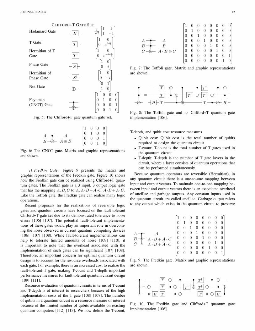
The design of quantum arithmetic circuits based on Clif-ford+T gates has caught the attention of researchers [101][100] [102] [103]. Figure 5 presents the quantum gates in theClifford+T gate set with their matrix and graphic representa-tions. The Clifford+T quantum gate set can be used to realizemulti-qubit logic gates such as the Toffoli and Fredkin gatespreviously presented in the literature [104] [105]. These multi-qubit gates will prove useful for describing the implementationof quantum circuits presented in this article.
a) CNOT Gate: Figure 6 presents the matrix and graphicrepresentations of the CNOT gate. The CNOT gate is aClifford+T gate (see figure 5). The CNOT gate is a 2 input, 2output logic gate and has the mapping A,B to A,A⊕B.
b) Toffoli Gate: Figure 7 presents the matrix and graphicrepresentations of the Toffoli gate. Figure 8 shows an exampleClifford+T quantum gate implementation of the Toffoli gate.The Toffoli gate is a 3 input, 3 output logic gate that hasthe mapping A,B,C to A,B,A · B ⊕ C. With appropriateinput combinations, the Toffoli gate can realize many logicoperations such as AND, OR and NAND.
JOURNAL HEADER 12
CLIFFORD+T GATE SET
Hadamard Gate H1√2
[1 11 −1
]T Gate T
[1 00 ei·
π4
]Hermitian of TGate T †
[1 00 e−i·
π4
]Phase Gate S
[1 00 i
]Hermitian ofPhase Gate S†
[1 00 −i
]Not Gate
[0 11 0
]Feynman(CNOT) Gate
•
1 0 0 00 1 0 00 0 0 10 0 1 0
Fig. 5: The Clifford+T gate quantum gate set.
A • A
B A⊕B
1 0 0 00 1 0 00 0 0 10 0 1 0
Fig. 6: The CNOT gate. Matrix and graphic representationsare shown.
c) Fredkin Gate: Figure 9 presents the matrix andgraphic representations of the Fredkin gate. Figure 10 showshow the Fredkin gate can be realized using Clifford+T quan-tum gates. The Fredkin gate is a 3 input, 3 output logic gatethat has the mapping A,B,C to A,A ·B+A ·C,A ·B+A ·C.Like the Toffoli gate, the Fredkin gate can realize many logicoperations.
Recent proposals for the realizations of reversible logicgates and quantum circuits have focused on the fault tolerantClifford+T gate set due to its demonstrated tolerance to noiseerrors [106] [107]. The potential fault-tolerant implementa-tions of these gates would play an important role in overcom-ing the noise observed in current quantum computing devices[106] [107] [108]. While fault-tolerant implementations canhelp to tolerate limited amounts of noise [109] [110], itis important to note that the overhead associated with theimplementation of such gates can be significant [107] [108].Therefore, an important concern for optimal quantum circuitdesign is to account for the resource overheads associated witheach gate. For example, there is an increased cost to realize thefault-tolerant T gate, making T-count and T-depth importantperformance measures for fault tolerant quantum circuit design[109] [111].
Resource evaluation of quantum circuits in terms of T-countand T-depth is of interest to researchers because of the highimplementation costs of the T gate [108] [107]. The numberof qubits in a quantum circuit is a resource measure of interestbecause of the limited number of qubits available on existingquantum computers [112] [113]. We now define the T-count,
A • A
B • B
C A ·B ⊕ C
1 0 0 0 0 0 0 00 1 0 0 0 0 0 00 0 1 0 0 0 0 00 0 0 1 0 0 0 00 0 0 0 1 0 0 00 0 0 0 0 1 0 00 0 0 0 0 0 0 10 0 0 0 0 0 1 0
Fig. 7: The Toffoli gate. Matrix and graphic representationsare shown.
• T • • T † •
• = T • T † T † •
H T • T • H
Fig. 8: The Toffoli gate and its Clifford+T quantum gateimplementation [106].
T-depth, and qubit cost resource measures.• Qubit cost: Qubit cost is the total number of qubits
required to design the quantum circuit.• T-count: T-count is the total number of T gates used in
the quantum circuit• T-depth: T-depth is the number of T gate layers in the
circuit, where a layer consists of quantum operations thatcan be performed simultaneously.
Because quantum operators are reversible (Hermitian), inany quantum circuit there is a one-to-one mapping betweeninput and output vectors. To maintain one-to-one mapping be-tween input and output vectors there is an associated overheadof ancillae and garbage outputs. Any constant inputs used inthe quantum circuit are called ancillae. Garbage output refersto any output which exists in the quantum circuit to preserve
A • AB × A ·B +A · CC × A ·B +A · C
1 0 0 0 0 0 0 00 1 0 0 0 0 0 00 0 1 0 0 0 0 00 0 0 1 0 0 0 00 0 0 0 1 0 0 00 0 0 0 0 0 1 00 0 0 0 0 1 0 00 0 0 0 0 0 0 1
Fig. 9: The Fredkin gate. Matrix and graphic representationsare shown.
• T • • T † •
× = T • T † T † •
× • H T • T • H •
Fig. 10: The Fredkin gate and Clifford+T quantum gateimplementation [106].
JOURNAL HEADER 13
one-to-one mapping but are neither one of the primary inputsnor a useful output. The inputs regenerated at the circuit outputare not considered garbage outputs [105]. Ancillae and garbageoutputs are circuit overheads that need to be minimized. Anideal quantum circuit must be garbageless in nature. Bennett’sgarbage removal scheme can be applied to design garbagelessquantum circuits[114].
For example, consider a quantum circuit that has a signifi-cant number of garbage outputs. The garbage outputs can beremoved by using Bennett’s garbage removal scheme [114].Figure 11 illustrates the Bennett’s garbage removal scheme.Let U represent an arbitrary quantum circuit that performsf(x1, x2, · · · , xn−1, xn) and let U−1 represent its logicalreverse.
|x1〉
U
|x1〉...
...|xn〉 |xn〉|0〉 Garbage
|0〉 |f(x1, · · · , xn)〉
(a) After Step 1
|x1〉
U
|x1〉...
...|xn〉 |xn〉|0〉 Garbage
|0〉 • |f(x1, · · · , xn)〉|0〉 |f(x1, · · · , xn)〉
(b) After Step 2|x1〉
U U−1
|x1〉...
...|xn〉 |xn〉|0〉 |0〉|0〉 • |0〉|0〉 |f(x1, · · · , xn)〉
(c) After Step 3
Fig. 11: Illustration of the Bennett’s garbage removal scheme.
Bennett’s garbage removal scheme is a three-step progress.After U is applied, all desired outputs are copied to ancillaewith CNOT gates. Then, U−1 is applied to the qubits of theoriginal circuit U . Thus, at the end of computation, the garbageoutputs have been restored to their initial values.
A. Quantum Arithmetic CircuitsThe quantum logic gates presented in the previous section
can be combined to create quantum arithmetic circuits to im-plement quantum algorithms. Quantum circuits for arithmeticoperations such as addition, subtraction and multiplicationbased on these gates have been proposed the literature [101][102] [103] [115], and in this section, we illustrate a recentquantum addition circuit and a recent quantum multiplicationcircuit.
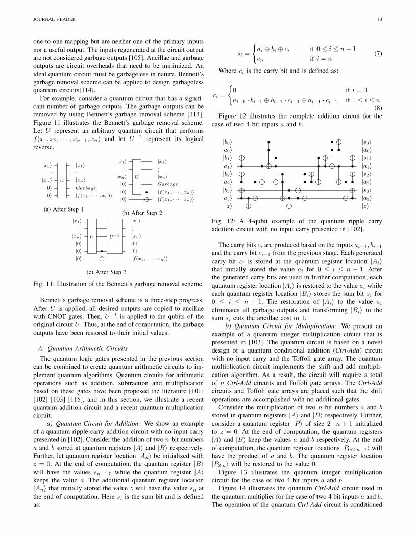
a) Quantum Circuit for Addition: We show an exampleof a quantum ripple carry addition circuit with no input carrypresented in [102]. Consider the addition of two n-bit numbersa and b stored at quantum registers |A〉 and |B〉 respectively.Further, let quantum register location |An〉 be initialized withz = 0. At the end of computation, the quantum register |B〉will have the values sn−1:0 while the quantum register |A〉keeps the value a. The additional quantum register location|An〉 that initially stored the value z will have the value sn atthe end of computation. Here si is the sum bit and is definedas:
si =
{ai ⊕ bi ⊕ ci if 0 ≤ i ≤ n− 1
cn if i = n(7)
Where ci is the carry bit and is defined as:
ci =
{0 if i = 0
ai−1 · bi−1 ⊕ bi−1 · ci−1 ⊕ ai−1 · ci−1 if 1 ≤ i ≤ n(8)
Figure 12 illustrates the complete addition circuit for thecase of two 4 bit inputs a and b.
|b0〉 • • |s0〉|a0〉 • • • |a0〉|b1〉 • • |s1〉|a1〉 • • • • • • • |a1〉|b2〉 • • |s2〉|a2〉 • • • • • • • |a2〉|b3〉 • |s3〉|a3〉 • • • • • |a3〉|z〉 |z〉
Fig. 12: A 4-qubit example of the quantum ripple carryaddition circuit with no input carry presented in [102].
The carry bits ci are produced based on the inputs ai−1, bi−1and the carry bit ci−1 from the previous stage. Each generatedcarry bit ci is stored at the quantum register location |Ai〉that initially stored the value ai for 0 ≤ i ≤ n − 1. Afterthe generated carry bits are used in further computation, eachquantum register location |Ai〉 is restored to the value ai whileeach quantum register location |Bi〉 stores the sum bit si for0 ≤ i ≤ n − 1. The restoration of |Ai〉 to the value aieliminates all garbage outputs and transforming |Bi〉 to thesum si cuts the ancillae cost to 1.
b) Quantum Circuit for Multiplication: We present anexample of a quantum integer multiplication circuit that ispresented in [103]. The quantum circuit is based on a noveldesign of a quantum conditional addition (Ctrl-Add) circuitwith no input carry and the Toffoli gate array. The quantummultiplication circuit implements the shift and add multipli-cation algorithm. As a result, the circuit will require a totalof n Ctrl-Add circuits and Toffoli gate arrays. The Ctrl-Addcircuits and Toffoli gate arrays are placed such that the shiftoperations are accomplished with no additional gates.
Consider the multiplication of two n bit numbers a and bstored in quantum registers |A〉 and |B〉 respectively. Further,consider a quantum register |P 〉 of size 2 · n + 1 initializedto z = 0. At the end of computation, the quantum registers|A〉 and |B〉 keep the values a and b respectively. At the endof computation, the quantum register locations |P0:2·n−1〉 willhave the product of a and b. The quantum register location|P2·n〉 will be restored to the value 0.
Figure 13 illustrates the quantum integer multiplicationcircuit for the case of two 4 bit inputs a and b.
Figure 14 illustrates the quantum Ctrl-Add circuit used inthe quantum multiplier for the case of two 4 bit inputs a and b.The operation of the quantum Ctrl-Add circuit is conditioned
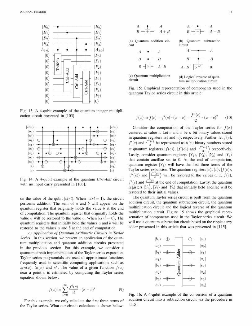
JOURNAL HEADER 14
|B0〉 • |B0〉|B1〉 • |B1〉|B2〉 • |B2〉|B3〉 • |B3〉|A3:0〉 • • • • |A3:0〉|0〉
Toff
olis
|P0〉|0〉
Ctr
l-A
dd|P1〉
|0〉
Ctr
l-A
dd
|P2〉|0〉
Ctr
l-A
dd
|P3〉|0〉 |P4〉|0〉 |P5〉|0〉 |P6〉|0〉 |P7〉|0〉 |0〉
Fig. 13: A 4-qubit example of the quantum integer multipli-cation circuit presented in [103]
|ctrl〉 • • • • • • |ctrl〉|b0〉 • • |s0〉|a0〉 • • • |a0〉|b1〉 • • |s1〉|a1〉 • • • • • • • |a1〉|b2〉 • • |s2〉|a2〉 • • • • • • • |a2〉|b3〉 • • |s3〉|a3〉 • • • • • • |a3〉|z〉 |s4〉|z〉 • |z〉
Fig. 14: A 4-qubit example of the quantum Ctrl-Add circuitwith no input carry presented in [103].
on the value of the qubit |ctrl〉. When |ctrl = 1〉, the circuitperforms addition. The sum of a and b will appear on thequantum register that originally holds the value b at the endof computation. The quantum register that originally holds thevalue a will be restored to the value a. When |ctrl = 0〉, Thequantum registers that initially hold the values a and b will berestored to the values a and b at the end of computation.
c) Application of Quantum Arithmetic Circuits in TaylorSeries: In this section, we present an application of the quan-tum multiplication and quantum addition circuits presentedin the previous section. For this example, we consider aquantum circuit implementation of the Taylor series expansion.Taylor series polynomials are used to approximate functionsfrequently used in scientific computing applications such assin(x), ln(x) and ex. The value of a given function f(x)near a point c is estimated by computing the Taylor seriesequation shown below:
f(x) ≈∞∑i=0
f i(c)
i!· (x− c)i (9)
For this example, we only calculate the first three terms ofthe Taylor series. What our circuit calculates is shown below:
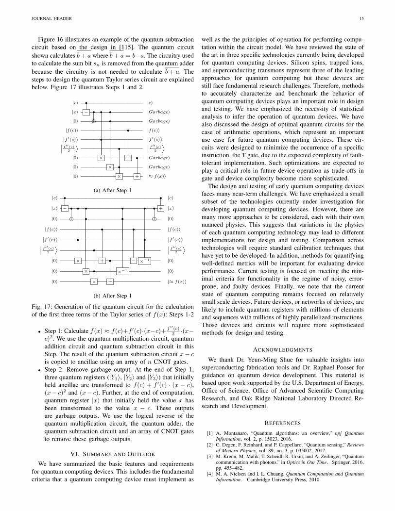
A • A
B + A+B
(a) Quantum addition cir-cuit
A • A
B − A−B
(b) Quantum subtractioncircuit
A • A
B • B
0 × A ·B
(c) Quantum multiplicationcircuit
A • A
B • B
A ·B ×−1 0
(d) Logical reverse of quan-tum multiplication circuit
Fig. 15: Graphical representation of components used in thequantum Taylor series circuit in this article.
f(x) ≈ f(c) + f ′(c) · (x− c) +f ′′(c)
2· (x− c)2 (10)
Consider the computation of the Taylor series for f(x)centered at value c. Let c and x be n bit binary values storedin quantum registers |x〉 and |c〉, respectively. Further, let f(c),f ′(c) and f ′′(c)
2 be represented as n bit binary numbers storedat quantum registers |f(c)〉, |f ′(c)〉 and
∣∣∣ f ′′(c)2
⟩respectively.
Lastly, consider quantum registers |Y1〉, |Y2〉, |Y3〉 and |Y4〉that contain ancillae set to 0. At the end of computation,quantum register |Y4〉 will have the first three terms of theTaylor series expansion. The quantum registers |c〉, |x〉, |f(c)〉,|f ′(c)〉 and
∣∣∣ f ′′(c)2
⟩will be restored to the values c, x, f(c),
f ′(c) and f ′′(c)2 at the end of computation. Lastly, the quantum
registers |Y1〉, |Y2〉 and |Y3〉 that initially held ancillae will berestored to their initial values.
The quantum Taylor series circuit is built from the quantumaddition circuit, the quantum subtraction circuit, the quantummultiplication circuit and the logical reverse of the quantummultiplication circuit. Figure 15 shows the graphical repre-sentation of components used in the Taylor series circuit. Wewill use a quantum subtraction circuit based on the ripple carryadder presented in this article that was presented in [115].
|b0〉
Qua
ntum
Add
er
|s0〉|a0〉 |a0〉|b1〉 |s1〉|a1〉 |a1〉|b2〉 |s2〉|a2〉 |a2〉|b3〉 |s3〉|a3〉 |a3〉
Fig. 16: A 4-qubit example of the conversion of a quantumaddition circuit into a subtraction circuit via the procedure in[115].
JOURNAL HEADER 15
Figure 16 illustrates an example of the quantum subtractioncircuit based on the design in [115]. The quantum circuitshown calculates b+ a where b+ a = b−a. The circuitry usedto calculate the sum bit sn is removed from the quantum adderbecause the circuitry is not needed to calculate b+ a. Thesteps to design the quantum Taylor series circuit are explainedbelow. Figure 17 illustrates Steps 1 and 2.
|c〉 • |c〉
|x〉 − • • • |Garbage〉
|0〉 • |Garbage〉
|f(c)〉 • |f(c)〉∣∣f ′(c)⟩ •∣∣f ′(c)⟩∣∣∣ f′′(c)2
⟩•
∣∣∣ f′′(c)2
⟩|0〉 × + • |Garbage〉
|0〉 × • |Garbage〉
|0〉 × + |≈ f(x)〉
(a) After Step 1|c〉 • • |c〉
|x〉 − • • • • • • + |x〉
|0〉 • • |0〉
|f(c)〉 • • |f(c)〉∣∣f ′(c)⟩ • •∣∣f ′(c)⟩∣∣∣ f′′(c)2
⟩•
∣∣∣ f′′(c)2
⟩|0〉 × + • − ×−1 |0〉
|0〉 × • ×−1 |0〉
|0〉 × + |≈ f(x)〉
(b) After Step 1
Fig. 17: Generation of the quantum circuit for the calculationof the first three terms of the Taylor series of f(x): Steps 1-2
• Step 1: Calculate f(x) ≈ f(c)+f ′(c)·(x−c)+ f ′′(c)2 ·(x−
c)2. We use the quantum multiplication circuit, quantumaddition circuit and quantum subtraction circuit in thisStep. The result of the quantum subtraction circuit x− cis copied to ancillae using an array of n CNOT gates.
• Step 2: Remove garbage output. At the end of Step 1,three quantum registers (|Y1〉, |Y2〉 and |Y3〉) that initiallyheld ancillae are transformed to f(c) + f ′(c) · (x − c),(x− c)2 and (x− c). Further, at the end of computation,quantum register |x〉 that initially held the value x hasbeen transformed to the value x − c. These outputsare garbage outputs. We use the logical reverse of thequantum multiplication circuit, the quantum adder, thequantum subtraction circuit and an array of CNOT gatesto remove these garbage outputs.
VI. SUMMARY AND OUTLOOK
We have summarized the basic features and requirementsfor quantum computing devices. This includes the fundamentalcriteria that a quantum computing device must implement as
well as the the principles of operation for performing compu-tation within the circuit model. We have reviewed the state ofthe art in three specific technologies currently being developedfor quantum computing devices. Silicon spins, trapped ions,and superconducting transmons represent three of the leadingapproaches for quantum computing but these devices arestill face fundamental research challenges. Therefore, methodsto accurately characterize and benchmark the behavior ofquantum computing devices plays an important role in designand testing. We have emphasized the necessity of statisticalanalysis to infer the operation of quantum devices. We havealso discussed the design of optimal quantum circuits for thecase of arithmetic operations, which represent an importantuse case for future quantum computing devices. These cir-cuits were designed to minimize the occurrence of a specificinstruction, the T gate, due to the expected complexity of fault-tolerant implementation. Such optimizations are expected toplay a critical role in future device operation as trade-offs ingate and device complexity become more sophisticated.
The design and testing of early quantum computing devicesfaces many near-term challenges. We have emphasized a smallsubset of the technologies currently under investigation fordeveloping quantum computing devices. However, there aremany more approaches to be considered, each with their ownnuanced physics. This suggests that variations in the physicsof each quantum computing technology may lead to differentimplementations for design and testing. Comparison acrosstechnologies will require standard calibration techniques thathave yet to be developed. In addition, methods for quantifyingwell-defined metrics will be important for evaluating deviceperformance. Current testing is focused on meeting the min-imal criteria for functionality in the regime of noisy, error-prone, and faulty devices. Finally, we note that the currentstate of quantum computing remains focused on relativelysmall scale devices. Future devices, or networks of devices, arelikely to include quantum registers with millions of elementsand sequences with millions of highly parallelized instructions.Those devices and circuits will require more sophisticatedmethods for design and testing.
ACKNOWLEDGMENTS
We thank Dr. Yeun-Ming Shue for valuable insights intosuperconducting fabrication tools and Dr. Raphael Pooser forguidance on quantum device development. This material isbased upon work supported by the U.S. Department of Energy,Office of Science, Office of Advanced Scientific ComputingResearch, and Oak Ridge National Laboratory Directed Re-search and Development.
REFERENCES
[1] A. Montanaro, “Quantum algorithms: an overview,” npj QuantumInformation, vol. 2, p. 15023, 2016.
[2] C. Degen, F. Reinhard, and P. Cappellaro, “Quantum sensing,” Reviewsof Modern Physics, vol. 89, no. 3, p. 035002, 2017.
[3] M. Krenn, M. Malik, T. Scheidl, R. Ursin, and A. Zeilinger, “Quantumcommunication with photons,” in Optics in Our Time. Springer, 2016,pp. 455–482.
[4] M. A. Nielsen and I. L. Chuang, Quantum Computation and QuantumInformation. Cambridge University Press, 2010.
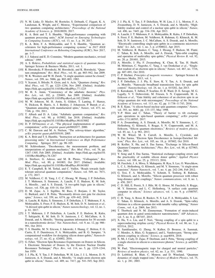
JOURNAL HEADER 16
[5] N. M. Linke, D. Maslov, M. Roetteler, S. Debnath, C. Figgatt, K. A.Landsman, K. Wright, and C. Monroe, “Experimental comparison oftwo quantum computing architectures,” Proceedings of the NationalAcademy of Sciences, p. 201618020, 2017.
[6] K. A. Britt and T. S. Humble, “High-performance computing withquantum processing units,” ACM Journal on Emerging Technologiesin Computing Systems (JETC), vol. 13, no. 3, p. 39, 2017.
[7] K. A. Britt, F. A. Mohiyaddin, and T. S. Humble, “Quantum ac-celerators for high-performance computing systems,” in 2017 IEEEInternational Conference on Rebooting Computing (ICRC), Nov 2017,pp. 1–7.
[8] J. J. Sakurai and E. D. Commins, “Modern quantum mechanics, revisededition,” 1995.
[9] A. S. Holevo, Probabilistic and statistical aspects of quantum theory.Springer Science & Business Media, 2011, vol. 1.
[10] R. Horodecki, P. Horodecki, M. Horodecki, and K. Horodecki, “Quan-tum entanglement,” Rev. Mod. Phys., vol. 81, pp. 865–942, Jun 2009.
[11] W. K. Wootters and W. H. Zurek, “A single quantum cannot be cloned,”Nature, vol. 299, no. 5886, pp. 802–803, 1982.
[12] V. Scarani, S. Iblisdir, N. Gisin, and A. Acın, “Quantum cloning,” Rev.Mod. Phys., vol. 77, pp. 1225–1256, Nov 2005. [Online]. Available:https://link.aps.org/doi/10.1103/RevModPhys.77.1225
[13] M. H. S. Amin, “Consistency of the adiabatic theorem,” Phys.Rev. Lett., vol. 102, p. 220401, Jun 2009. [Online]. Available:https://link.aps.org/doi/10.1103/PhysRevLett.102.220401
[14] M. W. Johnson, M. H. Amin, S. Gildert, T. Lanting, F. Hamze,N. Dickson, R. Harris, A. J. Berkley, J. Johansson, P. Bunyk et al.,“Quantum annealing with manufactured spins,” Nature, vol. 473, no.7346, p. 194, 2011.
[15] T. Albash and D. A. Lidar, “Adiabatic quantum computation,” Rev.Mod. Phys., vol. 90, p. 015002, Jan 2018. [Online]. Available:https://link.aps.org/doi/10.1103/RevModPhys.90.015002
[16] D. P. DiVincenzo et al., “The physical implementation of quantumcomputation,” arXiv preprint quant-ph/0002077, 2000.
[17] C. M. Dawson and M. A. Nielsen, “The solovay-kitaev algorithm,”arXiv preprint quant-ph/0505030, 2005.
[18] K. A. Britt and T. S. Humble, “Instruction set architectures for quantumprocessing units,” in International Conference on High PerformanceComputing. Springer, 2017, pp. 98–105.
[19] M. Schlosshauer, “Decoherence, the measurement problem, andinterpretations of quantum mechanics,” Rev. Mod. Phys., vol. 76, pp.1267–1305, Feb 2005. [Online]. Available: https://link.aps.org/doi/10.1103/RevModPhys.76.1267
[20] A. Streltsov, G. Adesso, and M. B. Plenio, “Colloquium,” Rev.Mod. Phys., vol. 89, p. 041003, Oct 2017. [Online]. Available:https://link.aps.org/doi/10.1103/RevModPhys.89.041003
[21] E. T. Campbell, B. M. Terhal, and C. Vuillot, “Roads towards fault-tolerant universal quantum computation,” Nature, vol. 549, no. 7671,p. 172, 2017.
[22] M. Veldhorst, C. H. Yang, J. C. C. Hwang, W. Huang, J. P. Dehollain,J. T. Muhonen, S. Simmons, A. Laucht, F. E. Hudson, K. M. Itoh,A. Morello, , and A. S. Dzurak, “A two-qubit logic gate in silicon,”Nature, vol. 526, pp. 410–14, Oct 2015.
[23] D. M. Zajac, A. J. Sigillito, M. Russ, F. Borjans, J. M. Taylor,G. Burkard, and J. R. Petta, “Resonantly driven cnot gate for electronspins,” Science, vol. 359, no. 6374, pp. 439–442, 2018.
[24] A. Laucht, R. Kalra, S. Simmons, J. P. Dehollain, J. T. Muhonen, F. A.Mohiyaddin, S. Freer, F. E. Hudson, K. M. Itoh, D. N. Jamieson et al.,“A dressed spin qubit in silicon,” Nature nanotechnology, vol. 12, no. 1,p. 61, 2017.
[25] J. T. Muhonen, J. P. Dehollain, A. Laucht, F. E. Hudson, R. Kalra,T. Sekiguchi, K. M. Itoh, D. N. Jamieson, J. C. McCallum, A. S.Dzurak, and A. Morello, “Storing quantum information for 30 secondsin a nanoelectronic device,” Nat. Nanotechnol., vol. 9, no. 12, pp. 986–991, Oct 2014.
[26] T. S. Humble, M. N. Ericson, J. Jakowski, J. Huang, C. Britton, F. G.Curtis, E. F. Dumitrescu, F. A. Mohiyaddin, and B. G. Sumpter, “Acomputational workflow for designing silicon donor qubits,” Nanotech-nology, vol. 27, no. 42, p. 424002, 2016.
[27] G. Feher, “Electron Spin Resonance Experiments on Donors in Silicon.I. Electronic Structure of Donors by the Electron Nuclear DoubleResonance Technique,” Phys. Rev., vol. 114, no. 5, pp. 1219–1244,Jun 1959.
[28] J. J. Pla, K. Y. Tan, J. P. Dehollain, W. H. Lim, J. J. L. Morton, D. N.Jamieson, A. S. Dzurak, and A. Morello, “A single-atom electron spinqubit in silicon,” Nature, vol. 489, no. 7417, pp. 541–545, Sep 2012.
[29] J. J. Pla, K. Y. Tan, J. P. Dehollain, W. H. Lim, J. J. L. Morton, F. A.Zwanenburg, D. N. Jamieson, A. S. Dzurak, and A. Morello, “High-fidelity readout and control of a nuclear spin qubit in silicon,” Nature,vol. 496, no. 7445, pp. 334–338, Apr 2013.
[30] A. Laucht, J. T. Muhonen, F. A. Mohiyaddin, R. Kalra, J. P. Dehollain,S. Freer, F. E. Hudson, M. Veldhorst, R. Rahman, G. Klimeck, K. M.Itoh, D. N. Jamieson, J. C. McCallum, A. S. Dzurak, and A. Morello,“Electrically controlling single-spin qubits in a continuous microwavefield,” Sci. Adv., vol. 1, no. 3, p. e1500022, Apr 2015.
[31] M. Veldhorst, R. Ruskov, C. Yang, J. Hwang, F. Hudson, M. Flatte,C. Tahan, K. Itoh, A. Morello, and A. Dzurak, “Spin-orbit couplingand operation of multivalley spin qubits,” Physical Review B, vol. 92,no. 20, p. 201401, 2015.
[32] A. Morello, J. Pla, F. Zwanenburg, K. Chan, K. Tan, H. Huebl,M. Mottonen, C. Nugroho, C. Yang, J. van Donkelaar et al., “Single-shot readout of an electron spin in silicon,” Nature, vol. 467, no. 7316,pp. 687–691, Oct 2010.
[33] C. P. Slichter, Principles of magnetic resonance. Springer Science &Business Media, 2013, vol. 1.
[34] J. P. Dehollain, J. J. Pla, E. Siew, K. Y. Tan, A. S. Dzurak, andA. Morello, “Nanoscale broadband transmission lines for spin qubitcontrol,” Nanotechnology, vol. 24, no. 1, p. 015202, Jan 2013.
[35] E. Kawakami, T. Jullien, P. Scarlino, D. R. Ward, D. E. Savage, M. G.Lagally, V. V. Dobrovitski, M. Friesen, S. N. Coppersmith, M. A.Eriksson et al., “Gate fidelity and coherence of an electron spin in ansi/sige quantum dot with micromagnet,” Proceedings of the NationalAcademy of Sciences, vol. 113, no. 42, pp. 11 738–11 743, 2016.
[36] B. E. Kane, “A silicon-based nuclear spin quantum computer,” Nature,vol. 393, no. 6681, pp. 133–137, May 1998.
[37] Y.-P. Shim and C. Tahan, “Theory of barrier vs tilt exchangegate operations in spin-based quantum computing,” arXiv preprintarXiv:1711.00595, 2017.
[38] F. A. Zwanenburg, A. S. Dzurak, A. Morello, M. Y. Simmons, L. C.Hollenberg, G. Klimeck, S. Rogge, S. N. Coppersmith, and M. A.Eriksson, “Silicon quantum electronics,” Reviews of modern physics,vol. 85, no. 3, p. 961, 2013.
[39] W. M. Witzel, M. S. Carroll, A. Morello, L. Cywinski, andS. Das Sarma, “Electron Spin Decoherence in Isotope-Enriched Sil-icon,” Phys. Rev. Lett., vol. 105, no. 18, p. 187602, Oct 2010.
[40] B. Koiller, X. Hu, and S. Das Sarma, “Exchange in Silicon-BasedQuantum Computer Architecture,” Phys. Rev. Lett., vol. 88, p. 027903,Dec 2001.
[41] Y. Song and S. Das Sarma, “Statistical exchange-coupling errors andthe practicality of scalable silicon donor qubits,” Applied PhysicsLetters, vol. 109, no. 25, p. 253113, 2016.
[42] M. Fuechsle, J. A. Miwa, S. Mahapatra, H. Ryu, S. Lee, O. Warschkow,L. C. L. Hollenberg, G. Klimeck, and M. Y. Simmons, “A single-atomtransistor,” Nature Nanotech., vol. 7, no. 4, pp. 242–246, Feb 2012.
[43] G. Tosi, F. A. Mohiyaddin, V. Schmitt, S. Tenberg, R. Rahman,G. Klimeck, and A. Morello, “Silicon quantum processor with robustlong-distance qubit couplings,” Nature communications, vol. 8, no. 1,p. 450, 2017.
[44] C. D. Hill, E. Peretz, S. J. Hile, M. G. House, M. Fuechsle, S. Rogge,M. Y. Simmons, and L. C. Hollenberg, “A surface code quantumcomputer in silicon,” Science advances, vol. 1, no. 9, p. e1500707,2015.
[45] C. H. Yang, A. Rossi, R. Ruskov, N. S. Lai, F. A. Mohiyaddin, S. Lee,C. Tahan, G. Klimeck, A. Morello, and A. S. Dzurak, “Spin-valleylifetimes in a silicon quantum dot with tunable valley splitting,” NatureComm., vol. 4, p. 2069, Jun 2013.
[46] T. Thorbeck and N. M. Zimmerman, “Formation of strain-inducedquantum dots in gated semiconductor nanostructures,” AIP Advances,vol. 5, no. 8, p. 087107, 2015.
[47] X. Hu, Y.-x. Liu, and F. Nori, “Strong coupling of a spin qubit to asuperconducting stripline cavity,” Physical Review B, vol. 86, no. 3, p.035314, 2012.
[48] N. Samkharadze, G. Zheng, N. Kalhor, D. Brousse, A. Sammak,U. Mendes, A. Blais, G. Scappucci, and L. Vandersypen, “Strong spin-photon coupling in silicon,” Science, p. eaar4054, 2018.
[49] X. Mi, J. Cady, D. Zajac, P. Deelman, and J. Petta, “Strong coupling ofa single electron in silicon to a microwave photon,” Science, p. aal2469,2016.
[50] W. Paul, “Electromagnetic traps for charged and neutral particles,”Reviews of modern physics, vol. 62, no. 3, p. 531, 1990.
[51] D. Leibfried, R. Blatt, C. Monroe, and D. Wineland, “Quantumdynamics of single trapped ions,” Reviews of Modern Physics, vol. 75,no. 1, p. 281, 2003.
JOURNAL HEADER 17
[52] R. Blatt and D. Wineland, “Entangled states of trapped atomic ions,”Nature, vol. 453, no. 7198, p. 1008, 2008.
[53] E. Mount, S.-Y. Baek, M. Blain, D. Stick, D. Gaultney, S. Crain,R. Noek, T. Kim, P. Maunz, and J. Kim, “Single qubit manipulation ina microfabricated surface electrode ion trap,” New Journal of Physics,vol. 15, no. 9, p. 093018, 2013.
[54] R. Blatt, H. Haffner, C. Roos, C. Becher, and F. Schmidt-Kaler,“Ion trap quantum computing with ca+ ions,” Quantum InformationProcessing, vol. 3, no. 1-5, pp. 61–73, 2004.
[55] B. B. Blinov, D. Leibfried, C. Monroe, and D. J. Wineland, “Quantumcomputing with trapped ion hyperfine qubits,” Quantum InformationProcessing, vol. 3, no. 1-5, pp. 45–59, 2004.
[56] P. T. Fisk, M. J. Sellars, M. A. Lawn, and G. Coles, “Accu-rate measurement of the 12.6 ghz” clock” transition in trapped/sup171/yb/sup+/ions,” IEEE transactions on ultrasonics, ferroelectrics,and frequency control, vol. 44, no. 2, pp. 344–354, 1997.
[57] A. D. Ludlow, M. M. Boyd, J. Ye, E. Peik, and P. O. Schmidt, “Opticalatomic clocks,” Reviews of Modern Physics, vol. 87, no. 2, p. 637, 2015.
[58] S. Debnath, “A programmable five qubit quantum computer usingtrapped atomic ions,” Ph.D. dissertation, University of Maryland,College Park, 2016.
[59] C. Monroe and J. Kim, “Scaling the ion trap quantum processor,”Science, vol. 339, no. 6124, pp. 1164–1169, 2013.
[60] H. Haffner, C. F. Roos, and R. Blatt, “Quantum computing with trappedions,” Physics reports, vol. 469, no. 4, pp. 155–203, 2008.
[61] R. Blume-Kohout, J. K. Gamble, E. Nielsen, K. Rudinger, J. Mizrahi,K. Fortier, and P. Maunz, “Demonstration of qubit operations belowa rigorous fault tolerance threshold with gate set tomography,” Naturecommunications, vol. 8, 2017.
[62] K. R. Brown, J. Kim, and C. Monroe, “Co-designing a scalable quan-tum computer with trapped atomic ions,” npj Quantum Information,vol. 2, p. 16034, 2016.
[63] D. J. Wineland, C. Monroe, W. M. Itano, D. Leibfried, B. E. King,and D. M. Meekhof, “Experimental issues in coherent quantum-statemanipulation of trapped atomic ions,” Journal of Research of theNational Institute of Standards and Technology, vol. 103, no. 3, p.259, 1998.
[64] D. Kielpinski, C. Monroe, and D. J. Wineland, “Architecture for alarge-scale ion-trap quantum computer,” Nature, vol. 417, no. 6890, p.709, 2002.
[65] J. Koch, M. Y. Terri, J. Gambetta, A. A. Houck, D. Schuster, J. Majer,A. Blais, M. H. Devoret, S. M. Girvin, and R. J. Schoelkopf, “Charge-insensitive qubit design derived from the cooper pair box,” PhysicalReview A, vol. 76, no. 4, p. 042319, 2007.
[66] S. M. Girvin, “Circuit qed: Superconducting qubits coupled to mi-crowave photons,” Proceedings of the 2011 Les Houches SummerSchool, 2011.
[67] G. Wendin, “Quantum information processing with superconductingcircuits: a review,” Reports on Progress in Physics, vol. 80, no. 10, p.106001, 2017.
[68] A. Blais, R.-S. Huang, A. Wallraff, S. M. Girvin, and R. J. Schoelkopf,“Cavity quantum electrodynamics for superconducting electrical cir-cuits: An architecture for quantum computation,” Physical Review A,vol. 69, no. 6, p. 062320, 2004.
[69] J. Majer, J. Chow, J. Gambetta, J. Koch, B. Johnson, J. Schreier,L. Frunzio, D. Schuster, A. Houck, A. Wallraff et al., “Couplingsuperconducting qubits via a cavity bus,” Nature, vol. 449, no. 7161,p. 443, 2007.
[70] J. M. Martinis and A. Megrant, “Ucsb final report for the csq program:Review of decoherence and materials physics for superconductingqubits,” arXiv preprint arXiv:1410.5793, 2014.
[71] O. Dial, D. T. McClure, S. Poletto, G. Keefe, M. B. Rothwell, J. M.Gambetta, D. W. Abraham, J. M. Chow, and M. Steffen, “Bulkand surface loss in superconducting transmon qubits,” SuperconductorScience and Technology, vol. 29, no. 4, p. 044001, 2016.
[72] V. Ambegaokar and A. Baratoff, “Tunneling between superconductors,”Physical Review Letters, vol. 10, no. 11, p. 486, 1963.
[73] S. J. Bosman, M. F. Gely, V. Singh, A. Bruno, D. Bothner, andG. A. Steele, “Multi-mode ultra-strong coupling in circuit quantumelectrodynamics,” npj Quantum Information, vol. 3, no. 1, p. 46, 2017.
[74] S. T. Flammia and Y.-K. Liu, “Direct fidelity estimation from few paulimeasurements,” Physical Review Letters, vol. 106, no. 23, jun 2011.
[75] M. P. da Silva, O. Landon-Cardinal, and D. Poulin, “Practical charac-terization of quantum devices without tomography,” Physical ReviewLetters, vol. 107, no. 21, nov 2011.
[76] E. Magesan, J. M. Gambetta, and J. Emerson, “Characterizing quantumgates via randomized benchmarking,” Physical Review A, vol. 85, no. 4,apr 2012.
[77] E. Magesan, J. M. Gambetta, B. R. Johnson, C. A. Ryan, J. M. Chow,S. T. Merkel, M. P. da Silva, G. A. Keefe, M. B. Rothwell, T. A. Ohki,M. B. Ketchen, and M. Steffen, “Efficient measurement of quantumgate error by interleaved randomized benchmarking,” Physical ReviewLetters, vol. 109, no. 8, aug 2012.
[78] S. Kimmel, M. P. da Silva, C. A. Ryan, B. R. Johnson, and T. Ohki,“Robust extraction of tomographic information via randomized bench-marking,” Physical Review X, vol. 4, no. 1, mar 2014.
[79] J. P. Gaebler, A. M. Meier, T. R. Tan, R. Bowler, Y. Lin, D. Hanneke,J. D. Jost, J. P. Home, E. Knill, D. Leibfried, and D. J. Wineland,“Randomized benchmarking of multiqubit gates,” Physical ReviewLetters, vol. 108, no. 26, jun 2012.
[80] T. Chasseur and F. K. Wilhelm, “Complete randomized benchmarkingprotocol accounting for leakage errors,” Physical Review A, vol. 92,no. 4, oct 2015.
[81] J. M. Gambetta, A. D. Corcoles, S. T. Merkel, B. R. Johnson, J. A.Smolin, J. M. Chow, C. A. Ryan, C. Rigetti, S. Poletto, T. A. Ohki,M. B. Ketchen, and M. Steffen, “Characterization of addressability bysimultaneous randomized benchmarking,” Physical Review Letters, vol.109, no. 24, dec 2012.
[82] H. Ball, T. M. Stace, S. T. Flammia, and M. J. Biercuk, “Effect ofnoise correlations on randomized benchmarking,” Physical Review A,vol. 93, no. 2, feb 2016.
[83] T. Proctor, K. Rudinger, K. Young, M. Sarovar, and R. Blume-Kohout,“What randomized benchmarking actually measures,” Physical ReviewLetters, vol. 119, no. 13, sep 2017.
[84] S. T. Merkel, J. M. Gambetta, J. A. Smolin, S. Poletto, A. D. Corcoles,B. R. Johnson, C. A. Ryan, and M. Steffen, “Self-consistent quantumprocess tomography,” Physical Review A, vol. 87, no. 6, jun 2013.
[85] R. Blume-Kohout, J. K. Gamble, E. Nielsen, K. Rudinger, J. Mizrahi,K. Fortier, and P. Maunz, “Demonstration of qubit operations belowa rigorous fault tolerance threshold with gate set tomography,” NatureCommunications, vol. 8, feb 2017.
[86] J. P. Dehollain, J. T. Muhonen, R. Blume-Kohout, K. M. Rudinger,J. K. Gamble, E. Nielsen, A. Laucht, S. Simmons, R. Kalra, A. S.Dzurak, and A. Morello, “Optimization of a solid-state electron spinqubit using gate set tomography,” New Journal of Physics, vol. 18,no. 10, p. 103018, oct 2016.
[87] C. Macchiavello and M. Rossi, “Quantum channel detection,” PhysicalReview A, vol. 88, no. 4, oct 2013.
[88] C. Granade, C. Ferrie, and D. G. Cory, “Accelerated randomizedbenchmarking,” New Journal of Physics, vol. 17, no. 1, p. 013042,jan 2015.
[89] F. Huszar and N. M. T. Houlsby, “Adaptive bayesian quantum tomog-raphy,” Physical Review A, vol. 85, no. 5, may 2012.
[90] D. H. Mahler, L. A. Rozema, A. Darabi, C. Ferrie, R. Blume-Kohout,and A. M. Steinberg, “Adaptive quantum state tomography improvesaccuracy quadratically,” Physical Review Letters, vol. 111, no. 18, oct2013.
[91] J. Chen, H. Dawkins, Z. Ji, N. Johnston, D. Kribs, F. Shultz, andB. Zeng, “Uniqueness of quantum states compatible with given mea-surement results,” Physical Review A, vol. 88, no. 1, jul 2013.
[92] G. Toth, W. Wieczorek, D. Gross, R. Krischek, C. Schwemmer,and H. Weinfurter, “Permutationally invariant quantum tomography,”Physical Review Letters, vol. 105, no. 25, dec 2010.
[93] D. Gross, Y.-K. Liu, S. T. Flammia, S. Becker, and J. Eisert, “Quantumstate tomography via compressed sensing,” Physical Review Letters,vol. 105, no. 15, oct 2010.
[94] S. Boixo, S. V. Isakov, V. N. Smelyanskiy, R. Babbush, N. Ding,Z. Jiang, M. J. Bremner, J. M. Martinis, and H. Neven, “CharacterizingQuantum Supremacy in Near-Term Devices,” ArXiv e-prints, Jul. 2016.
[95] O. Landon-Cardinal and D. Poulin, “Practical learning method formulti-scale entangled states,” New Journal of Physics, vol. 14, no. 8,p. 085004, aug 2012.
[96] C. E. Granade, C. Ferrie, N. Wiebe, and D. G. Cory, “Robust onlinehamiltonian learning,” New Journal of Physics, vol. 14, no. 10, p.103013, oct 2012.
[97] G. Carleo and M. Troyer, “Solving the quantum many-body problemwith artificial neural networks,” Science, vol. 355, no. 6325, pp. 602–606, feb 2017.
[98] D.-L. Deng, X. Li, and S. D. Sarma, “Quantum entanglement in neuralnetwork states,” Physical Review X, vol. 7, no. 2, may 2017.
JOURNAL HEADER 18
[99] N. S. Yanofsky and M. A. Mannucci, Quantum Computing for Com-puter Scientists, 1st ed. New York, NY, USA: Cambridge UniversityPress, 2008.
[100] M. K. Bhaskar, S. Hadfield, A. Papageorgiou, and I. Petras, “Quan-tum Algorithms and Circuits for Scientific Computing,” QUANTUMINFORMATION & COMPUTATION, vol. 16, no. 3-4, pp. 197–236,MARCH 2016.
[101] C.-C. Lin, A. Chakrabarti, and N. K. Jha, “Qlib: Quantum modulelibrary,” J. Emerg. Technol. Comput. Syst., vol. 11, no. 1, pp. 7:1–7:20,Oct. 2014. [Online]. Available: http://doi.acm.org/10.1145/2629430
[102] H. Thapliyal and N. Ranganathan, “Design of efficient reversiblelogic-based binary and bcd adder circuits,” J. Emerg. Technol. Comput.Syst., vol. 9, no. 3, pp. 17:1–17:31, Oct. 2013. [Online]. Available:http://doi.acm.org/10.1145/2491682
[103] E. Munoz-Coreas and H. Thapliyal, “T-count Optimized Design ofQuantum Integer Multiplication,” ArXiv e-prints, Jun. 2017.
[104] T. Toffoli, “Reversible computing,” in Proceedings of the 7thColloquium on Automata, Languages and Programming. London,UK, UK: Springer-Verlag, 1980, pp. 632–644. [Online]. Available:http://dl.acm.org/citation.cfm?id=646234.682540
[105] E. Fredkin and T. Toffoli, “Conservative logic,” International Journalof Theoretical Physics, vol. 21, no. 3, pp. 219–253, Apr 1982.[Online]. Available: https://doi.org/10.1007/BF01857727
[106] M. Amy, D. Maslov, M. Mosca, and M. Roetteler, “A meet-in-the-middle algorithm for fast synthesis of depth-optimal quantum circuits,”IEEE Transactions on Computer-Aided Design of Integrated Circuitsand Systems, vol. 32, no. 6, pp. 818–830, June 2013.
[107] S. J. Devitt, A. M. Stephens, W. J. Munro, and K. Nemoto, “Re-quirements for fault-tolerant factoring on an atom-optics quantumcomputer,” Nature Communications, vol. 4, p. 2524, Oct. 2013.
[108] M. B. Hastings and J. Haah, “Distillation with sublogarithmic over-head,” ArXiv e-prints, Sep. 2017.
[109] M. Amy, D. Maslov, and M. Mosca, “Polynomial-time t-depth opti-mization of clifford+t circuits via matroid partitioning,” IEEE Trans-actions on Computer-Aided Design of Integrated Circuits and Systems,vol. 33, no. 10, pp. 1476–1489, Oct 2014.
[110] E. Knill, “Fault-Tolerant Postselected Quantum Computation:Schemes,” eprint arXiv:quant-ph/0402171, Feb. 2004.
[111] D. Gosset, V. Kliuchnikov, M. Mosca, and V. Russo, “Analgorithm for the t-count,” Quantum Information & Computation,vol. 14, no. 15-16, pp. 1261–1276, 2014. [Online]. Available:http://www.rintonpress.com/xxqic14/qic-14-1516/1261-1276.pdf
[112] D. Lu, K. Li, J. Li, H. Katiyar, A. J. Park, G. Feng, T. Xin,H. Li, G. Long, A. Brodutch, J. Baugh, B. Zeng, and R. Laflamme,“Enhancing quantum control by bootstrapping a quantum processor of12 qubits,” npj Quantum Information, vol. 3, p. 45, Oct. 2017.
[113] C. Song, K. Xu, W. Liu, C.-p. Yang, S.-B. Zheng, H. Deng, Q. Xie,K. Huang, Q. Guo, L. Zhang, P. Zhang, D. Xu, D. Zheng, X. Zhu,H. Wang, Y.-A. Chen, C.-Y. Lu, S. Han, and J.-W. Pan, “10-QubitEntanglement and Parallel Logic Operations with a SuperconductingCircuit,” Physical Review Letters, vol. 119, no. 18, p. 180511, Nov.2017.
[114] C. H. Bennett, “Logical reversibility of computation,” IBM J. Res.Dev., vol. 17, no. 6, pp. 525–532, Nov. 1973. [Online]. Available:http://dx.doi.org/10.1147/rd.176.0525
[115] H. Thapliyal, “Mapping of subtractor and adder-subtractor circuits onreversible quantum gates,” in Transactions on Computational ScienceXXVII. Springer, 2016, pp. 10–34.