quantum optical properties of a dipole emitter … · quantum optical properties of a dipole...
TRANSCRIPT
Quantum optical properties of a dipole emitter coupled to an ɛ-near-zero nanoscale waveguide
Ruzan Sokhoyan* and Harry A. Atwater Thomas J. Watson Laboratories of Applied Physics, California Institute of Technology, Pasadena, California 91125,
USA *[email protected]
Abstract: We study quantum optical properties of a dipole emitter coupled to a rectangular nanoscale waveguide with dielectric core and silver cladding. We investigate enhanced spontaneous emission and the photonic Lamb shift for emitters whose resonant frequencies are near the waveguide frequency cutoff where the waveguide behaves as an ɛ-near-zero metamaterial. Via a dyadic Green’s function-based field quantization scheme, we calculate the photonic Lamb shift as well as the spontaneous emission enhancement and spectrum. Using realistic parameters for typical quantum emitters, we suggest experimentally realizable schemes to observe relatively large photonic Lamb shifts in waveguides.
©2013 Optical Society of America
OCIS codes: (270.5580) Quantum electrodynamics; (020.3690) Line shapes and shifts; (240.6680) Surface plasmons; (250.5403) Plasmonics; (160.3918) Metamaterials.
References and links 1. Y. M. Liu and X. Zhang, “Metamaterials: a new frontier of science and technology,” Chem. Soc. Rev. 40(5),
2494–2507 (2011). 2. J. B. Pendry, “Negative refraction makes a perfect lens,” Phys. Rev. Lett. 85(18), 3966–3969 (2000). 3. J. B. Pendry, D. Schurig, and D. R. Smith, “Controlling electromagnetic fields,” Science 312(5781), 1780–1782
(2006). 4. K. L. Tsakmakidis, A. D. Boardman, and O. Hess, “‘Trapped rainbow’ storage of light in metamaterials,” Nature
450(7168), 397–401 (2007). 5. A. Alù and N. Engheta, “Dielectric sensing in epsilon-near-zero narrow waveguide channels,” Phys. Rev. B
78(4), 045102 (2008). 6. M. G. Silveirinha and N. Engheta, “Theory of supercoupling, squeezing wave energy, and field confinement in
narrow channels and tight bends using epsilon near-zero metamaterials,” Phys. Rev. B 76(24), 245109 (2007). 7. A. Alu and N. Engheta, “Coaxial-to-waveguide matching with epsilon-near-zero ultranarrow channels and
bends,” IEEE Trans. Antennas Propag. 58(2), 328–339 (2010). 8. A. Alù and N. Engheta, “Boosting molecular fluorescence with a plasmonic nanolauncher,” Phys. Rev. Lett.
103(4), 043902 (2009). 9. B. Edwards, A. Alù, M. E. Young, M. Silveirinha, and N. Engheta, “Experimental verification of epsilon-near-
zero metamaterial coupling and energy squeezing using a microwave waveguide,” Phys. Rev. Lett. 100(3), 033903 (2008).
10. E. J. R. Vesseur, T. Coenen, H. Caglayan, N. Engheta, and A. Polman, “Experimental verification of n = 0 structures for visible light,” Phys. Rev. Lett. 110(1), 013902 (2013).
11. R. H. Dicke, “Coherence in spontaneous radiation processes,” Phys. Rev. 93(1), 99–110 (1954). 12. P. J. Yao, C. Van Vlack, A. Reza, M. Patterson, M. M. Dignam, and S. Hughes, “Ultrahigh Purcell factors and
Lamb shifts in slow-light metamaterial waveguides,” Phys. Rev. B 80(19), 195106 (2009). 13. P. Sheng, Introduction to Wave Scattering, Localization, and Mesoscopic Phenomena, 2nd ed., Springer Series
in Materials Science (Springer, 2006), 333 pp. 14. E. M. Purcell, “Spontaneous emission probabilities at radio frequencies,” Phys. Rev. 69, 681 (1946). 15. K. J. Vahala, “Optical microcavities,” Nature 424(6950), 839–846 (2003). 16. A. V. Akimov, A. Mukherjee, C. L. Yu, D. E. Chang, A. S. Zibrov, P. R. Hemmer, H. Park, and M. D. Lukin,
“Generation of single optical plasmons in metallic nanowires coupled to quantum dots,” Nature 450(7168), 402–406 (2007).
17. K. J. Russell, T. L. Liu, S. Y. Cui, and E. L. Hu, “Large spontaneous emission enhancement in plasmonic nanocavities,” Nat. Photonics 6(7), 459–462 (2012).
18. T. Quang, M. Woldeyohannes, S. John, and G. S. Agarwal, “Coherent control of spontaneous emission near a photonic band edge: A single-atom optical memory device,” Phys. Rev. Lett. 79(26), 5238–5241 (1997).
#199182 - $15.00 USD Received 8 Oct 2013; revised 9 Dec 2013; accepted 11 Dec 2013; published 19 Dec 2013(C) 2013 OSA 30 December 2013 | Vol. 21, No. 26 | DOI:10.1364/OE.21.032279 | OPTICS EXPRESS 32279
19. X. H. Wang, B. Y. Gu, R. Z. Wang, and H. Q. Xu, “Decay kinetic properties of atoms in photonic crystals with absolute gaps,” Phys. Rev. Lett. 91(11), 113904 (2003).
20. N. Vats, S. John, and K. Busch, “Theory of fluorescence in photonic crystals,” Phys. Rev. A 65(4), 043808 (2002).
21. W. E. Lamb and R. C. Retherford, “Fine structure of the hydrogen atom by a microwave method,” Phys. Rev. 72(3), 241–243 (1947).
22. H. A. Bethe, “The electromagnetic shift of energy levels,” Phys. Rev. 72(4), 339–341 (1947). 23. X. H. Wang, Y. S. Kivshar, and B. Y. Gu, “Giant lamb shift in photonic crystals,” Phys. Rev. Lett. 93(7),
073901 (2004). 24. Q. Liu, H. W. Song, W. Wang, X. Bai, Y. Wang, B. A. Dong, L. Xu, and W. Han, “Observation of Lamb shift
and modified spontaneous emission dynamics in the YBO3:Eu3+ inverse opal,” Opt. Lett. 35(17), 2898–2900 (2010).
25. J. M. Wylie and J. E. Sipe, “Quantum electrodynamics near an interface. II,” Phys. Rev. A 32(4), 2030–2043 (1985).
26. H. T. Dung, L. Knoll, and D. G. Welsch, “Three-dimensional quantization of the electromagnetic field in dispersive and absorbing inhomogeneous dielectrics,” Phys. Rev. A 57(5), 3931–3942 (1998).
27. G. Colas des Francs, J. Grandidier, S. Massenot, A. Bouhelier, J.-C. Weeber, and A. Dereux, “Integrated plasmonic waveguides: A mode solver based on density of states formulation,” Phys. Rev. B 80(11), 115419 (2009).
28. T. W. Ebbesen, H. J. Lezec, H. F. Ghaemi, T. Thio, and P. A. Wolff, “Extraordinary optical transmission through sub-wavelength hole arrays,” Nature 391(6668), 667–669 (1998).
29. T. T. Minh, K. Tanaka, and M. Tanaka, “Complex propagation constants of surface plasmon polariton rectangular waveguide by method of lines,” Opt. Express 16(13), 9378–9390 (2008).
30. M. A. Swillam and A. S. Helmy, “Analysis and applications of 3D rectangular metallic waveguides,” Opt. Express 18(19), 19831–19843 (2010).
31. L. Novotny and B. Hecht, Principles of Nano-optics (Cambridge University, 2006), 539 pp. 32. F. J. García de Abajo and A. Howie, “Relativistic electron energy loss and electron-induced photon emission in
inhomogeneous dielectrics,” Phys. Rev. Lett. 80(23), 5180–5183 (1998). 33. F. J. García de Abajo and A. Howie, “Retarded field calculation of electron energy loss in inhomogeneous
dielectrics,” Phys. Rev. B 65(11), 115418 (2002). 34. E. D. Palik and G. Ghosh, Handbook of Optical Constants of Solids (Academic, 1998). 35. Y. C. Jun, R. Pala, and M. L. Brongersma, “Strong modification of quantum dot spontaneous emission via gap
plasmon coupling in metal nanoslits,” J. Phys. Chem. C 114(16), 7269–7273 (2010). 36. Y. C. Jun, R. D. Kekatpure, J. S. White, and M. L. Brongersma, “Nonresonant enhancement of spontaneous
emission in metal-dielectric-metal plasmon waveguide structures,” Phys. Rev. B 78(15), 153111 (2008). 37. J. A. Dionne, L. A. Sweatlock, H. A. Atwater, and A. Polman, “Plasmon slot waveguides: Towards chip-scale
propagation with subwavelength-scale localization,” Phys. Rev. B 73(3), 035407 (2006). 38. T. Hümmer, F. J. Garcia-Vidal, L. Martin-Moreno, and D. Zueco, “Weak and strong coupling regimes in
plasmonic QED,” Phys. Rev. B 87(11), 115419 (2013). 39. G. Khitrova, H. M. Gibbs, M. Kira, S. W. Koch, and A. Scherer, “Vacuum Rabi splitting in semiconductors,”
Nat. Phys. 2(2), 81–90 (2006). 40. M. O. Scully and M. S. Zubairy, Quantum Optics (Cambridge University, 1997). 41. R. Fleury and A. Alu, “Enhanced superradiance in epsilon-near-zero plasmonic channels,” Phys. Rev. B 87,
201101(R) (2013). 42. M. L. Andersen, S. Stobbe, A. S. Sorensen, and P. Lodahl, “Strongly modified plasmon-matter interaction with
mesoscopic quantum emitters,” Nat. Phys. 7(3), 215–218 (2011). 43. R. Fitzpatrick, “Quantum mechanics,” pp. 192–193. 44. Z. Ficek and R. Tanas, “Entangled states and collective nonclassical effects in two-atom systems,” Phys. Rep.
372(5), 369–443 (2002).
1. Introduction
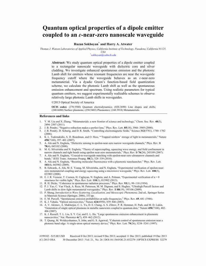
Metamaterials are artificial photonic structures with sub-wavelength features defined by the arrangements and interactions of the sub-wavelength elements and their interactions with electromagnetic field [1]. By rationally arranging these elements, one can create effective media with prescribed values of the electric permittivity ɛ and magnetic permeability µ. Metamaterials can give rise to interesting applications such as a “superlens” that overcomes the diffraction limit [2], design of optical cloaks [3], and light stopping [4]. Specific to our focus here, one can design the real part of the dielectric constant to have epsilon near zero (ENZ) near the waveguide frequency cutoff of a rectangular metallic waveguide with a dielectric core (Fig. 1) [5]. ENZ waveguides can enable interesting applications, such as supercoupling [6], antenna to waveguide coupling [7], and spontaneous emission enhancement which is insensitive to the emitter position within the waveguide [8].
#199182 - $15.00 USD Received 8 Oct 2013; revised 9 Dec 2013; accepted 11 Dec 2013; published 19 Dec 2013(C) 2013 OSA 30 December 2013 | Vol. 21, No. 26 | DOI:10.1364/OE.21.032279 | OPTICS EXPRESS 32280
As the frequency of fundamental mode of a waveguide approaches cutoff, the propagation constant approaches zero value, implying infinite effective wavelength, as demonstrated in the microwave [9] and visible [10] frequency ranges. This property makes ENZ waveguides attractive for observation of the cooperative behavior of quantum emitters, such as strong dipole-dipole interactions and superradiance [11]. In homogeneous electromagnetic media, the wavelength defines the spatial scale at which the interaction between emitters is significant: a very large wavelength implies a very low frequency. Near the waveguide cutoff frequency, the waveguide mode has extremely extended wavelength while its frequency may lie within an optical or telecom band [10]. Interestingly, near frequency cutoff in a rectangular metal waveguide with dielectric core, the group velocity assumes small values [6]. Slow light waveguides are of interest for quantum optics applications, since they enable one to attain high spontaneous emission enhancement [12]. For a lossless waveguide, the Purcell factor is inversely proportional to the group velocity of the waveguide mode [13]. In case of ENZ waveguide, one observes a significant enhancement of the local density of optical states (LDOS) in the dielectric core [10]. It has long been known that the spontaneous decay rate is not an intrinsic property of the emitter, but is function of the local density of optical states (LDOS) of the media to which it is coupled [14]. Coupling an emitter to an environment with tailored LDOS may substantially modify its decay rate, compared to its decay rate in free space [15–17]. ENZ waveguides are potentially useful in practical applications of spontaneous emission enhancement since the LDOS enhancement at the frequency cutoff does not vary along the waveguide length [10]. For further practical applications of ENZ waveguides, which imply embedding multiple quantum emitters in the waveguide core, it is important to know how the LDOS varies in the plane perpendicular to the longitudinal axis of the waveguide. It is also important to understand how varying geometrical parameters of the waveguide affects the spontaneous emission enhancement in the waveguide core.
The LDOS inside the waveguide core is a relatively rapidly-varying function of frequency near waveguide cutoff. It is known from photonic crystal theory that photonic band edge, where the photonic density of states varies abruptly, has a strong influence on electrodynamics of excited atoms in the photonic crystal, yielding enhanced quantum interference in spontaneous emission [18], nonclassical decay [19], and the Lamb shift [20]. The discovery [21] and explanation [22] of the vacuum Lamb shift lies at the foundations of modern quantum electrodynamics (QED). The Lamb shift is manifest as a resonant frequency shift of the emitter caused by the coupling of the bound electron to the vacuum modes. The Lamb shift for the hydrogen atom in an inverse-opal photonic crystal can be calculated [23]. The authors of Ref [23]. have assessed the vacuum and photonic contributions to the overall Lamb shift. By analyzing the 1s → 2p transition in the hydrogen, it has been shown that photonic Lamb shift in a photonic crystal may exceed the vacuum Lamb shift by one or two orders of magnitude, depending on the spatial position of the atom and the photonic lattice constant. Direct observation of the photonic Lamb shift in a photonic crystal has also been reported [24], where the photonic Lamb shift was measured as an emission frequency difference between a plain glass reference sample and a YbO3:Eu3+ inverse opal. The reported photonic Lamb shift was 0.9 nm at a wavelength of 710 nm. These experimental results showed good agreement with theoretical predictions [20]. Further, energy level shifts of the atoms, induced by a planar metal surface have been previously calculated [25]: the photonic Lamb shift becomes significant around the surface plasmon resonance frequency, and it changes its sign when crossing the resonance. Recently photonic Lamb shifts induced by a metamaterial slab waveguide have been calculated, and their rich frequency characteristics have been reported [12]. In this context it is interesting to understand the photonic Lamb shift for quantum emitters embedded in an ENZ waveguide.
In the present work, we employ a dyadic Green’s function-based field quantization scheme [26] to analyze the spontaneous emission enhancement, photonic Lamb shifts, and spontaneous emission spectrum for a quantum dipole emitter coupled to a rectangular ENZ
#199182 - $15.00 USD Received 8 Oct 2013; revised 9 Dec 2013; accepted 11 Dec 2013; published 19 Dec 2013(C) 2013 OSA 30 December 2013 | Vol. 21, No. 26 | DOI:10.1364/OE.21.032279 | OPTICS EXPRESS 32281
waveguide with dielectric core and silver cladding (see Fig. 1). By using the concept of the two-dimensional Green’s function [27], we analyze how the coupling efficiency varies with changes in the resonant frequency or dipole moment orientation of the emitter. Further, using finite difference time domain (FDTD) calculations we explore the dependence of dipole spontaneous emission enhancement on the waveguide geometry and emitter spatial position. Finally, we discuss the induced photonic Lamb shifts and spontaneous emission spectrum from the waveguide-emitter coupled system. By using realistic quantum emitter parameters, we show that nanoscale ENZ waveguides are a promising platform for observation of large photonic Lamb shifts.
Fig. 1. Rectangular waveguide with dielectric core and metal cladding.
2. Mode structure and LDOS variation in the waveguide core
From one viewpoint, light propagation in a waveguide near cutoff (Fig. 1) can be viewed as analogous to light transmission in subwavelength apertures. Transmission through subwavelength holes [28] has been widely investigated via different numerical techniques, such as the method of lines [29], FDTD and finite element methods [30] that allow one to define the eigenmodes of the structures and their main characteristics. It has been shown that for optical frequencies, where the perfect conductor approximation is not valid for metals, characteristics of the mode significantly change, compared to the cases when metals can be described as perfect electric conductors (PEC) [29]. For example at optical frequencies, the waveguide fundamental mode cutoff frequency considerably red shifts compared to the case of a waveguide composed of PEC walls. When analyzing the behavior of a dipole emitter it is important to know to which waveguide modes it will preferentially couple to, depending on the dipole orientation and its spatial location. To address this issue, we use the two-dimensional LDOS formulation [27]. The three-dimensional LDOS ( )rρ
is defined via the
dyadic Green’s function in the frequency domain ( , , )G r r ω′
. The directional LDOS ,inρ that
is the density of states to which the in
oriented dipole may couple (also referred to as partial
LDOS) is given as [31]
2
6Im ( , ) ( , , ),
in i in G r r n i x y zc
ωρπ
= =
(1)
where ω is the frequency of the electromagnetic field, and c is the speed of light in the vacuum. In Eq. (1), an inner product is taken on both sides of the dyadic Green’s function. The two-dimensional partial LDOS 2
i
Dnρ is defines as a spatial Fourier transform of the three-
dimensional partial LDOS inρ
2 ( , k , ) ( , ) d .z
i i
i k zDn z nr e r zρ ω ρ ω
∞−
−∞
=
(2)
Here kz is the z projection of the wave vector k
, and ( , )r x y=
. For a structure that is
translationally invariant in z direction, due to the boundary conditions imposed on the
#199182 - $15.00 USD Received 8 Oct 2013; revised 9 Dec 2013; accepted 11 Dec 2013; published 19 Dec 2013(C) 2013 OSA 30 December 2013 | Vol. 21, No. 26 | DOI:10.1364/OE.21.032279 | OPTICS EXPRESS 32282
electromagnetic fields, the z projection of the wave vector is a propagation constant. It has been previously demonstrated that the two-dimensional LDOS formulation is a powerful tool for finding the waveguide modes and defining their main characteristics [27]. One of the advantages of this method is that it straightforwardly extracts the kz-resolved information. We use the boundary element method (BEM) [32, 33] to calculate the two-dimensional LDOS of an infinite waveguide. In the BEM, calculations are performed in the frequency domain, and the only assumption is that the different materials in the structure are described by frequency-dependent local dielectric functions and the form abrupt interfaces with adjacent materials. Using the BEM, the electromagnetic field in each homogeneous region is expressed as a function of auxiliary boundary charges and currents. After boundary conditions are applied, a set of linear integrals is obtained and solved by discretization. The silver cladding of the rectangular waveguide (see Fig. 1) is characterized by a frequency-dependent complex refractive index imported to the BEM simulation as tabulated data from Palik [34]. It is assumed that the waveguide exterior is in air and the refractive index of the dielectric core is taken as nd = 1.49.
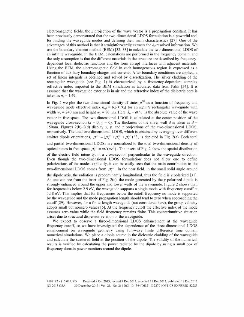
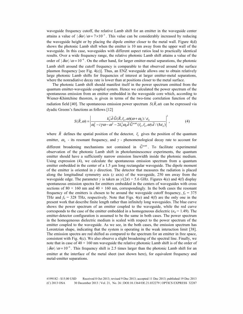
In Fig. 2 we plot the two-dimensional density of states ρ2D as a function of frequency and waveguide mode effective index neff = Re(kz/k0) for an infinite rectangular waveguide with width wx = 240 nm and height wy = 80 nm. Here 0 /k cω= is the absolute value of the wave
vector in free space. The two-dimensional LDOS is calculated at the center position of the waveguide cross-section (x = 0, y = 0). The thickness of the silver wall d is taken as d = 150nm. Figures 2(b)–2(d) display x, y, and z projections of the two-dimensional LDOS, respectively. The total two-dimensional LDOS, which is obtained by averaging over different emitter dipole orientations, 2 2 2 2( ) / 3
x y z
D D D Dn n nρ ρ ρ ρ= + + , is depicted in Fig. 2(a). Both total
and partial two-dimensional LDOSs are normalized to the total two-dimensional density of optical states in free space 2 2
0 / ( )D cρ ω π= . The insets of Fig. 2 show the spatial distribution
of the electric field intensity, in a cross-section perpendicular to the waveguide direction. Even though the two-dimensional LDOS formulation does not allow one to define polarizations of the modes explicitly, it can be easily seen that the main contribution to the two-dimensional LDOS comes from 2D
yρ . In the near field, in the small solid angle around
the dipole axis, the radiation is predominantly longitudinal, thus the field is y polarized [31]. As one can see from the inset of Fig. 2(c), the mode generated by the y polarized dipole is strongly enhanced around the upper and lower walls of the waveguide. Figure 2 shows that, for frequencies below 2.9 eV, the waveguide supports a single mode with frequency cutoff at 1.18 eV. This implies that for frequencies below the cutoff frequency no mode is supported by the waveguide and the mode propagation length should tend to zero when approaching the cutoff [29]. However, for a finite-length waveguide (not considered here), the group velocity adopts small but nonzero values [6]. At the frequency cutoff the effective index of the mode assumes zero value while the field frequency remains finite. This counterintuitive situation arises due to structural dispersion relation of the waveguide.
We expect to observe a three-dimensional LDOS enhancement at the waveguide frequency cutoff, so we have investigated the dependence of the three-dimensional LDOS enhancement on waveguide geometry using full-wave finite difference time domain numerical simulations. We place a dipole source in the dielectric cladding of the waveguide and calculate the scattered field at the position of the dipole. The validity of the numerical results is verified by calculating the power radiated by the dipole by using a small box of frequency domain power monitors around the dipole.
#199182 - $15.00 USD Received 8 Oct 2013; revised 9 Dec 2013; accepted 11 Dec 2013; published 19 Dec 2013(C) 2013 OSA 30 December 2013 | Vol. 21, No. 26 | DOI:10.1364/OE.21.032279 | OPTICS EXPRESS 32283
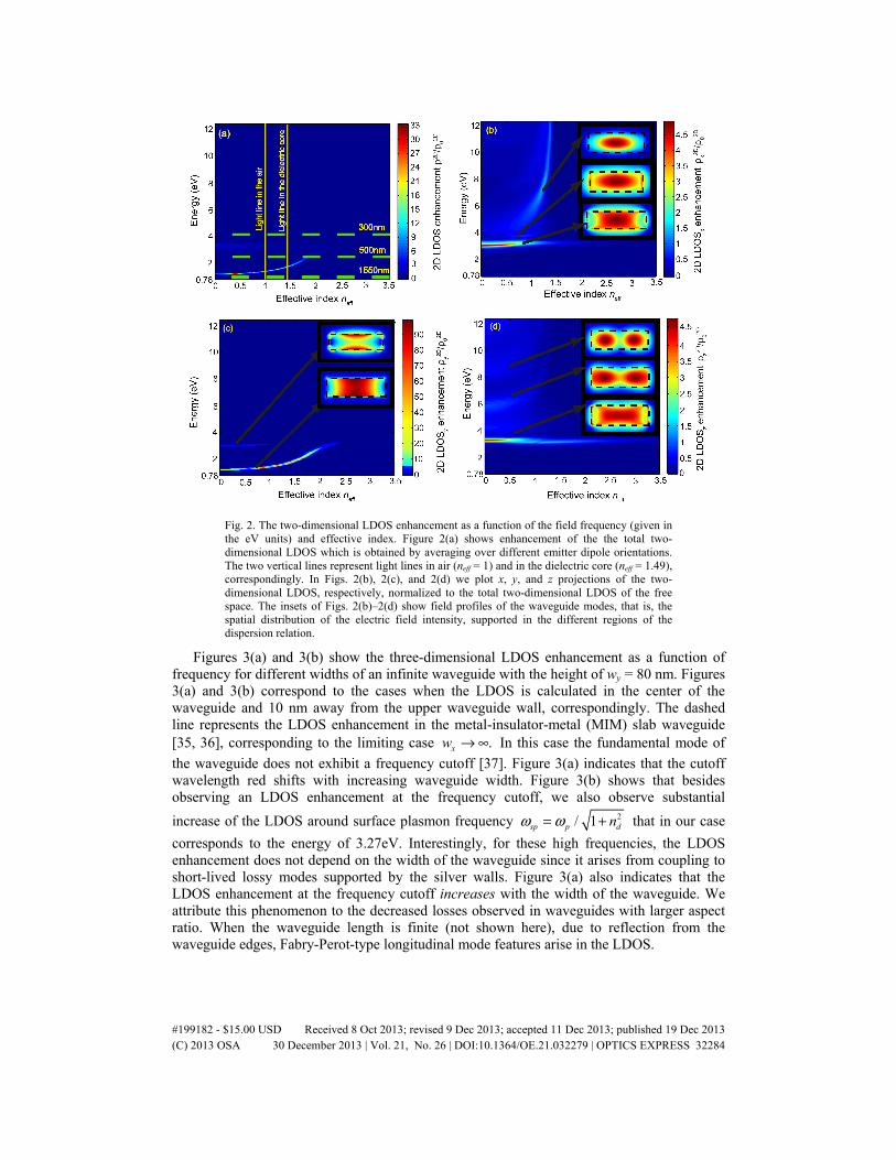
Fig. 2. The two-dimensional LDOS enhancement as a function of the field frequency (given in the eV units) and effective index. Figure 2(a) shows enhancement of the the total two-dimensional LDOS which is obtained by averaging over different emitter dipole orientations. The two vertical lines represent light lines in air (neff = 1) and in the dielectric core (neff = 1.49), correspondingly. In Figs. 2(b), 2(c), and 2(d) we plot x, y, and z projections of the two-dimensional LDOS, respectively, normalized to the total two-dimensional LDOS of the free space. The insets of Figs. 2(b)–2(d) show field profiles of the waveguide modes, that is, the spatial distribution of the electric field intensity, supported in the different regions of the dispersion relation.
Figures 3(a) and 3(b) show the three-dimensional LDOS enhancement as a function of frequency for different widths of an infinite waveguide with the height of wy = 80 nm. Figures 3(a) and 3(b) correspond to the cases when the LDOS is calculated in the center of the waveguide and 10 nm away from the upper waveguide wall, correspondingly. The dashed line represents the LDOS enhancement in the metal-insulator-metal (MIM) slab waveguide [35, 36], corresponding to the limiting case .xw → ∞ In this case the fundamental mode of
the waveguide does not exhibit a frequency cutoff [37]. Figure 3(a) indicates that the cutoff wavelength red shifts with increasing waveguide width. Figure 3(b) shows that besides observing an LDOS enhancement at the frequency cutoff, we also observe substantial
increase of the LDOS around surface plasmon frequency 2/ 1sp p dnω ω= + that in our case
corresponds to the energy of 3.27eV. Interestingly, for these high frequencies, the LDOS enhancement does not depend on the width of the waveguide since it arises from coupling to short-lived lossy modes supported by the silver walls. Figure 3(a) also indicates that the LDOS enhancement at the frequency cutoff increases with the width of the waveguide. We attribute this phenomenon to the decreased losses observed in waveguides with larger aspect ratio. When the waveguide length is finite (not shown here), due to reflection from the waveguide edges, Fabry-Perot-type longitudinal mode features arise in the LDOS.
#199182 - $15.00 USD Received 8 Oct 2013; revised 9 Dec 2013; accepted 11 Dec 2013; published 19 Dec 2013(C) 2013 OSA 30 December 2013 | Vol. 21, No. 26 | DOI:10.1364/OE.21.032279 | OPTICS EXPRESS 32284
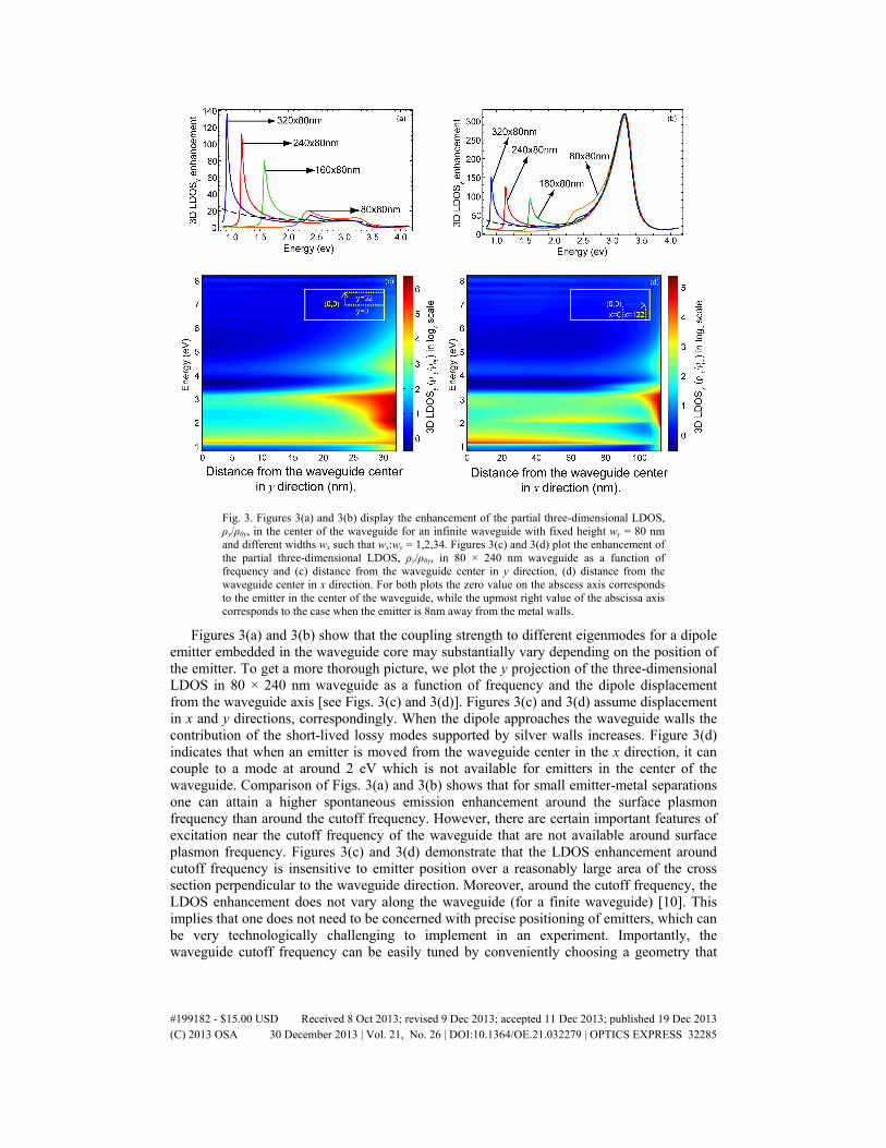
Fig. 3. Figures 3(a) and 3(b) display the enhancement of the partial three-dimensional LDOS, ρy/ρ0y, in the center of the waveguide for an infinite waveguide with fixed height wy = 80 nm and different widths wx such that wx:wy = 1,2,34. Figures 3(c) and 3(d) plot the enhancement of the partial three-dimensional LDOS, ρy/ρ0y, in 80 × 240 nm waveguide as a function of frequency and (c) distance from the waveguide center in y direction, (d) distance from the waveguide center in x direction. For both plots the zero value on the abscess axis corresponds to the emitter in the center of the waveguide, while the upmost right value of the abscissa axis corresponds to the case when the emitter is 8nm away from the metal walls.
Figures 3(a) and 3(b) show that the coupling strength to different eigenmodes for a dipole emitter embedded in the waveguide core may substantially vary depending on the position of the emitter. To get a more thorough picture, we plot the y projection of the three-dimensional LDOS in 80 × 240 nm waveguide as a function of frequency and the dipole displacement from the waveguide axis [see Figs. 3(c) and 3(d)]. Figures 3(c) and 3(d) assume displacement in x and y directions, correspondingly. When the dipole approaches the waveguide walls the contribution of the short-lived lossy modes supported by silver walls increases. Figure 3(d) indicates that when an emitter is moved from the waveguide center in the x direction, it can couple to a mode at around 2 eV which is not available for emitters in the center of the waveguide. Comparison of Figs. 3(a) and 3(b) shows that for small emitter-metal separations one can attain a higher spontaneous emission enhancement around the surface plasmon frequency than around the cutoff frequency. However, there are certain important features of excitation near the cutoff frequency of the waveguide that are not available around surface plasmon frequency. Figures 3(c) and 3(d) demonstrate that the LDOS enhancement around cutoff frequency is insensitive to emitter position over a reasonably large area of the cross section perpendicular to the waveguide direction. Moreover, around the cutoff frequency, the LDOS enhancement does not vary along the waveguide (for a finite waveguide) [10]. This implies that one does not need to be concerned with precise positioning of emitters, which can be very technologically challenging to implement in an experiment. Importantly, the waveguide cutoff frequency can be easily tuned by conveniently choosing a geometry that
#199182 - $15.00 USD Received 8 Oct 2013; revised 9 Dec 2013; accepted 11 Dec 2013; published 19 Dec 2013(C) 2013 OSA 30 December 2013 | Vol. 21, No. 26 | DOI:10.1364/OE.21.032279 | OPTICS EXPRESS 32285
exhibits ENZ behavior for the frequencies corresponding to typical quantum emitter resonant frequencies that may lie in the visible or telecommunications band.
3. Spontaneous emission spectrum and photonic Lamb shifts
We calculate the associated photonic Lamb shifts and spontaneous emission power spectrum for an emitter embedded in the dielectric core of the waveguide. We employ macroscopic quantum electrodynamic techniques which are well suited to describe a quantum emitter coupled to a dispersive and lossy environment [26]. It is known that the real part of the dyadic
Green's function ( , , )G r r ω′
diverges at r r′= . Hence for an inhomogeneous environment, it
is convenient to represent the Green’s function as hom scattG G G= +
, where homG
is the analytically known (divergent) expression for the Green’s function in a conveniently chosen
homogeneous environment (for example, free space or homogeneous dielectric), while scattG
is the contribution originating due to scattering of the radiation from the inhomogeneous structure. The Lamb shift induced by a homogeneous medium can be incorporated in the definition of the resonant frequency of the emitter, and we calculate the photonic Lamb shift induced by the scattering part of the Green's function [12]:
scatt
2 0 00
0
Re( ( , , )),L
d G r r dk
ωωε
Δ = −
(3)
where 0r
defines the spatial position of the emitter, d
is the transition dipole moment of the
emitter, – the reduced Planck constant, 0ε – the dielectric permittivity of the vacuum.
Equation (3) has been derived without application of Markov and rotating wave approximations, hence, it is applicable both in strong and weak interaction limits [38]. The photonic Lamb shift is proportional to the square of the dipole moment of the emitter hence a large dipole moment is a desirable characteristic of the emitter.
Narrow homogeneous linewidths and large dipole moment are characteristic of both interface-fluctuation quantum dots (QDs), such as GaAs QDs, and self-assembled QDs, such as In0.60Ga0.40As/GaAs QDs [39]. For interface fluctuation QDs a homogeneous linewidth of 5.6 GHz and dipole moments of d = 50–100 D (1D≈3.33564 × 10⁻³⁰ C·m) has been measured while for self-assembled QDs a homogeneous linewidth of 0.44 GHz and dipole moment of d = 25–35 D have been measured.
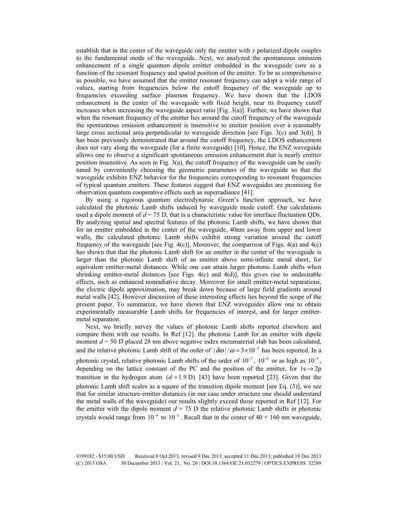
As a check, we calculate the photonic Lamb shift relative to free space induced by a semi-infinite silver sheet as a function of the resonant frequency of the emitter [Figs. 4(a) and 4(b)] [25]. We assume that the dipole emitter is suspended in the air above the silver sheet and its dipole moment is perpendicular to the sheet surface. The dipole moment of the emitter is chosen as d = 75 D, typical for self-assembled QDs. Figures 4(a) and 4(b) represent the cases when the emitter is 40 nm and 10 nm above the metal-air interface, correspondingly. For an emitter-metal distance of 40 nm, the relative photonic Lamb shift is of the order of
6| | / 10δω ω −= , while for an emitter distance of 10 nm, the photonic Lamb shift attains values
of the order of 4| | / 10δω ω −= over a wide frequency range.
We next investigated the photonic Lamb shifts (the frequency shift relative to homogeneous dielectric environment with 1.49dn = ) induced by an infinite length
rectangular waveguide with height equal to wy = 80 nm and different widths (see Fig. 1). The dipole moment of the emitter (d = 75 D) is oriented in y direction. Figure 4(c) plots the photonic Lamb shift as a function of frequency for different aspect ratios of the waveguide, assuming that the emitter is placed in the center of the waveguide. The black dashed line corresponds to the case of the MIM waveguide. Figure 4(c) shows that the absolute value of the photonic Lamb shift peaks at the frequency cutoff of the waveguide. Around the
#199182 - $15.00 USD Received 8 Oct 2013; revised 9 Dec 2013; accepted 11 Dec 2013; published 19 Dec 2013(C) 2013 OSA 30 December 2013 | Vol. 21, No. 26 | DOI:10.1364/OE.21.032279 | OPTICS EXPRESS 32286
waveguide frequency cutoff, the relative Lamb shift for an emitter in the waveguide center attains a value of 5| | / 7 10δω ω −= × . This value can be considerably increased by reducing
the waveguide height or by placing the dipole emitter closer to the metal wall. Figure 4(d) shows the photonic Lamb shift when the emitter is 10 nm away from the upper wall of the waveguide. In this case, waveguides with different aspect ratios lead to practically identical results. Over a wide frequency range, the relative photonic Lamb shift attains a value of the order of 4| | / 10δω ω −= . On the other hand, for larger emitter-metal separations, the photonic
Lamb shift around the cutoff frequency is comparable to that observed around the surface plasmon frequency [see Fig. 4(c)]. Thus, an ENZ waveguide allows one to obtain relatively large photonic Lamb shifts for frequencies of interest at larger emitter-metal separations, where the nonradiative decay rate is lower than at positions closer to the metal surface.
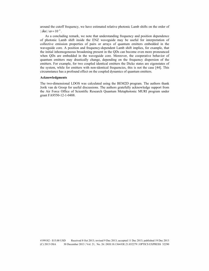
The photonic Lamb shift should manifest itself in the power spectrum emitted from the quantum emitter-waveguide coupled system. Hence we calculated the power spectrum of the spontaneous emission from an emitter embedded in the waveguide core which, according to Wiener-Khintchine theorem, is given in terms of the two-time correlation function of the
radiation field [40]. The spontaneous emission power spectrum ( , )S R ω
can be expressed via
dyadic Greens’s functions as follows [12]
220 0 0 0
2 2 2 scatt0 0 0 0 0 0
( , , )( ) /( , ) ,
2 ( , , ) / ( )
k d G R rS R
i k d G r r d
ω ω ω εωω γ ω ω ω ω ε
+=
− − −
(4)
where R
defines the spatial position of the detector, 0r
gives the position of the quantum
emitter, 0ω - its resonant frequency, and γ - phenomenological decay rate to account for
different broadening mechanisms not contained in scattG
. To facilitate experimental observation of the photonic Lamb shift in photoluminescence experiments, the quantum emitter should have a sufficiently narrow emission linewidth inside the photonic medium. Using expression (4), we calculate the spontaneous emission spectrum from a quantum emitter embedded in the center of a 1.5 µm long rectangular waveguide. The dipole moment of the emitter is oriented in y direction. The detector that measures the radiation is placed along the longitudinal symmetry axis (z axis) of the waveguide, 250 nm away from the waveguide edge. The parameter γ is taken as γ/(2π) = 5.6 GHz. Figures 4(e) and 4(f) display spontaneous emission spectra for emitters embedded in the centers of waveguides with cross sections of 80 × 160 nm and 40 × 160 nm, correspondingly. In the both cases the resonant frequency of the emitters is chosen to be around the waveguide cutoff frequency, f0 = 375 THz and f0 = 328 THz, respectively. Note that Figs. 4(e) and 4(f) are the only one in the present work that describe finite length rather than infinitely long waveguides. The blue curve shows the power spectrum of an emitter coupled to the waveguide, while the red curve corresponds to the case of the emitter embedded in a homogeneous dielectric (nd = 1.49). The emitter-detector configuration is assumed to be the same in both cases. The power spectrum in the homogeneous dielectric medium is scaled with respect to the power spectrum of the emitter coupled to the waveguide. As we see, in the both cases, the emission spectrum has Lorentzian shape, indicating that the system is operating in the weak interaction limit [38]. The emission spectra are red shifted as compared to the spectrum for an emitter in free space, consistent with Fig. 4(c). We also observe a slight broadening of the spectral line. Finally, we note that in case of 40 × 160 nm waveguide the relative photonic Lamb shift is of the order of
4| | / 10δω ω −= . This frequency shift is 2.5 times larger than the photonic Lamb shift for an
emitter at the interface of the metal sheet (not shown here), for equivalent frequency and metal-emitter separations.
#199182 - $15.00 USD Received 8 Oct 2013; revised 9 Dec 2013; accepted 11 Dec 2013; published 19 Dec 2013(C) 2013 OSA 30 December 2013 | Vol. 21, No. 26 | DOI:10.1364/OE.21.032279 | OPTICS EXPRESS 32287
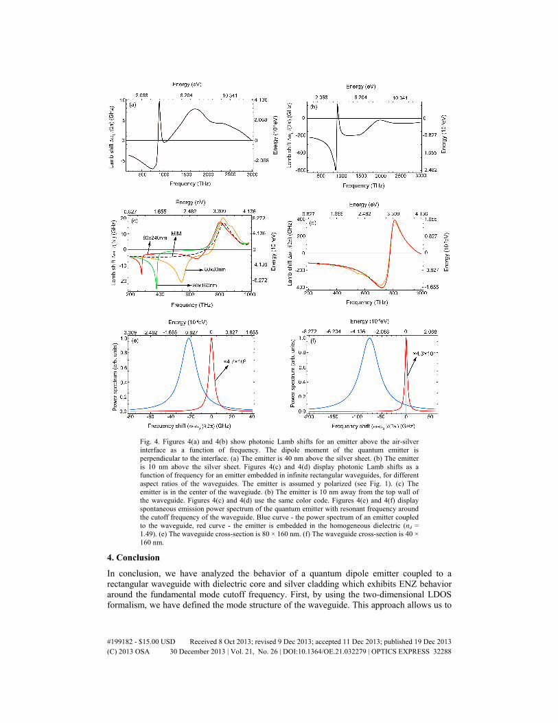
Fig. 4. Figures 4(a) and 4(b) show photonic Lamb shifts for an emitter above the air-silver interface as a function of frequency. The dipole moment of the quantum emitter is perpendicular to the interface. (a) The emitter is 40 nm above the silver sheet. (b) The emitter is 10 nm above the silver sheet. Figures 4(c) and 4(d) display photonic Lamb shifts as a function of frequency for an emitter embedded in infinite rectangular waveguides, for different aspect ratios of the waveguides. The emitter is assumed y polarized (see Fig. 1). (c) The emitter is in the center of the wavegiude. (b) The emitter is 10 nm away from the top wall of the waveguide. Figures 4(c) and 4(d) use the same color code. Figures 4(e) and 4(f) display spontaneous emission power spectrum of the quantum emitter with resonant frequency around the cutoff frequency of the waveguide. Blue curve - the power spectrum of an emitter coupled to the waveguide, red curve - the emitter is embedded in the homogeneous dielectric (nd = 1.49). (e) The waveguide cross-section is 80 × 160 nm. (f) The waveguide cross-section is 40 × 160 nm.
4. Conclusion
In conclusion, we have analyzed the behavior of a quantum dipole emitter coupled to a rectangular waveguide with dielectric core and silver cladding which exhibits ENZ behavior around the fundamental mode cutoff frequency. First, by using the two-dimensional LDOS formalism, we have defined the mode structure of the waveguide. This approach allows us to
#199182 - $15.00 USD Received 8 Oct 2013; revised 9 Dec 2013; accepted 11 Dec 2013; published 19 Dec 2013(C) 2013 OSA 30 December 2013 | Vol. 21, No. 26 | DOI:10.1364/OE.21.032279 | OPTICS EXPRESS 32288
establish that in the center of the waveguide only the emitter with y polarized dipole couples to the fundamental mode of the waveguide. Next, we analyzed the spontaneous emission enhancement of a single quantum dipole emitter embedded in the waveguide core as a function of the resonant frequency and spatial position of the emitter. To be as comprehensive as possible, we have assumed that the emitter resonant frequency can adopt a wide range of values, starting from frequencies below the cutoff frequency of the waveguide up to frequencies exceeding surface plasmon frequency. We have shown that the LDOS enhancement in the center of the waveguide with fixed height, near its frequency cutoff increases when increasing the waveguide aspect ratio [Fig. 3(a)]. Further, we have shown that when the resonant frequency of the emitter lies around the cutoff frequency of the waveguide the spontaneous emission enhancement is insensitive to emitter position over a reasonably large cross sectional area perpendicular to waveguide direction [see Figs. 3(c) and 3(d)]. It has been previously demonstrated that around the cutoff frequency, the LDOS enhancement does not vary along the waveguide (for a finite waveguide) [10]. Hence, the ENZ waveguide allows one to observe a significant spontaneous emission enhancement that is nearly emitter position insensitive. As seen in Fig. 3(a), the cutoff frequency of the waveguide can be easily tuned by conveniently choosing the geometric parameters of the waveguide so that the waveguide exhibits ENZ behavior for the frequencies corresponding to resonant frequencies of typical quantum emitters. These features suggest that ENZ waveguides are promising for observation quantum cooperative effects such as superradiance [41].
By using a rigorous quantum electrodynamic Green’s function approach, we have calculated the photonic Lamb shifts induced by waveguide mode cutoff. Our calculations used a dipole moment of d = 75 D, that is a characteristic value for interface fluctuation QDs. By analyzing spatial and spectral features of the photonic Lamb shifts, we have shown that for an emitter embedded in the center of the waveguide, 40nm away from upper and lower walls, the calculated photonic Lamb shifts exhibit strong variation around the cutoff frequency of the waveguide [see Fig. 4(c)]. Moreover, the comparison of Figs. 4(a) and 4(c) has shown that that the photonic Lamb shift for an emitter in the center of the waveguide is larger than the photonic Lamb shift of an emitter above semi-infinite metal sheet, for equivalent emitter-metal distances. While one can attain larger photonic Lamb shifts when shrinking emitter-metal distances [see Figs. 4(c) and 4(d)], this gives rise to undesirable effects, such as enhanced nonradiative decay. Moreover for small emitter-metal separations, the electric dipole approximation, may break down because of large field gradients around metal walls [42]. However discussion of these interesting effects lies beyond the scope of the present paper. To summarize, we have shown that ENZ waveguides allow one to obtain experimentally measurable Lamb shifts for frequencies of interest, and for larger emitter-metal separation.
Next, we briefly survey the values of photonic Lamb shifts reported elsewhere and compare them with our results. In Ref [12]. the photonic Lamb for an emitter with dipole moment d = 50 D placed 28 nm above negative index metamaterial slab has been calculated, and the relative photonic Lamb shift of the order of 5| | / 3 10δω ω −= × has been reported. In a
photonic crystal, relative photonic Lamb shifts of the order of 710− , 610− or as high as 510− , depending on the lattice constant of the PC and the position of the emitter, for 1s → 2p transition in the hydrogen atom ( 1.9 D)d ≈ [43] have been reported [23]. Given that the
photonic Lamb shift scales as a square of the transition dipole moment [see Eq. (3)], we see that for similar structure-emitter distances (in our case under structure one should understand the metal walls of the waveguide) our results slightly exceed those reported in Ref [12]. For the emitter with the dipole moment d = 75 D the relative photonic Lamb shifts in photonic crystals would range from 410− to 210− . Recall that in the center of 40 × 160 nm waveguide,
#199182 - $15.00 USD Received 8 Oct 2013; revised 9 Dec 2013; accepted 11 Dec 2013; published 19 Dec 2013(C) 2013 OSA 30 December 2013 | Vol. 21, No. 26 | DOI:10.1364/OE.21.032279 | OPTICS EXPRESS 32289
around the cutoff frequency, we have estimated relative photonic Lamb shifts on the order of 4| | / 10δω ω −= .
As a concluding remark, we note that understanding frequency and position dependence of photonic Lamb shift inside the ENZ waveguide may be useful for interpretation of collective emission properties of pairs or arrays of quantum emitters embedded in the waveguide core. A position and frequency-dependent Lamb shift implies, for example, that the initial inhomogeneous broadening present in the QDs can become even more pronounced when QDs are embedded in the waveguide core. Moreover, the cooperative behavior of quantum emitters may drastically change, depending on the frequency dispersion of the emitters. For example, for two coupled identical emitters the Dicke states are eigenstates of the system, while for emitters with non-identical frequencies, this is not the case [44]. This circumstance has a profound effect on the coupled dynamics of quantum emitters.
Acknowledgments
The two-dimensional LDOS was calculated using the BEM2D program. The authors thank Jorik van de Groep for useful discussions. The authors gratefully acknowledge support from the Air Force Office of Scientific Research Quantum Metaphotonic MURI program under grant FA9550-12-1-0488.
#199182 - $15.00 USD Received 8 Oct 2013; revised 9 Dec 2013; accepted 11 Dec 2013; published 19 Dec 2013(C) 2013 OSA 30 December 2013 | Vol. 21, No. 26 | DOI:10.1364/OE.21.032279 | OPTICS EXPRESS 32290