quantum transport in vdw heterostructures of …quantum transport in vdw heterostructures of...
TRANSCRIPT

Quantum transport in vdW heterostructuresof graphene and 2D materials
Tomoki Machida
Institute of Industrial Science, University of Tokyo
June 11, 2015
NPSMP (ISSP, Kashiwa)

OutlineTransfer technique of atomic layersQuantum Hall pnp junctions
Novel magnetoresistance oscillationsCoherent interference in QH edge channels
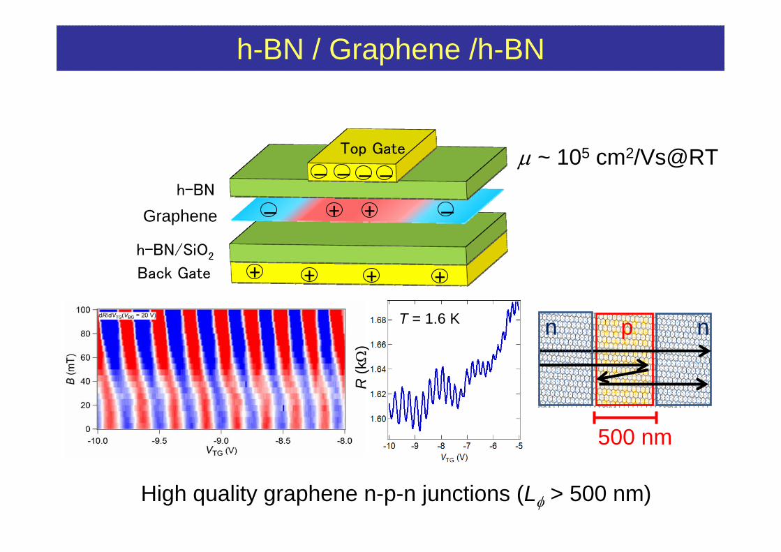
Graphene/h-BN
Josephson junctionsSupercurrentFraunhofer pattern and Fiske resonance
NbSe2/NbSe2
Magnetic tunnel junctionsMagnetoresistance effect
Fe0.25TaS2/Fe0.25TaS2
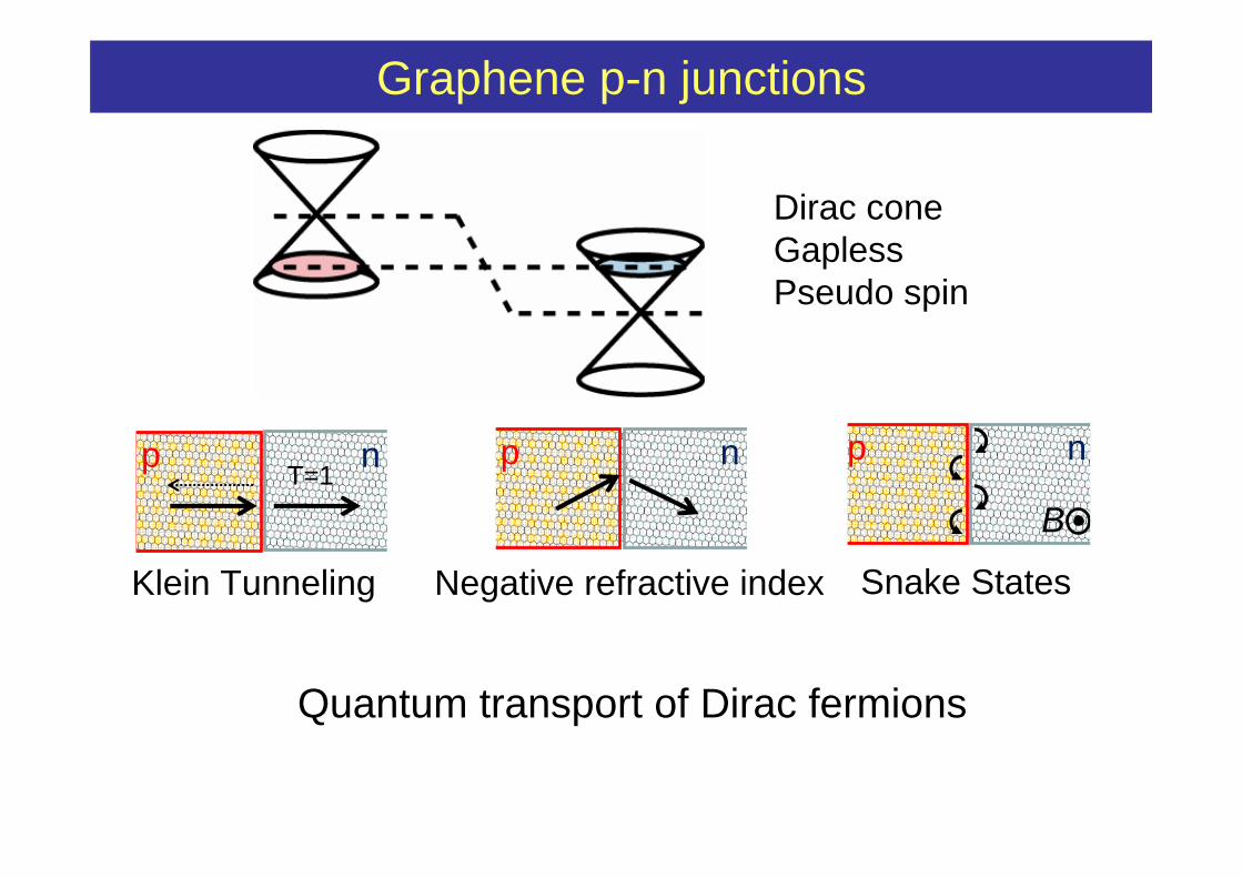
Graphene p-n junctions
Klein Tunneling
T=1p n
Negative refractive index
p n p n
Snake States
B
Quantum transport of Dirac fermions
Dirac coneGaplessPseudo spin

Graphene p-n junctions in high B
Landau quantizationQHE
Co-propagating quantum Hall edge channels
p nCounter-circulating quantum Hall edge channels
Novel resistance oscillations
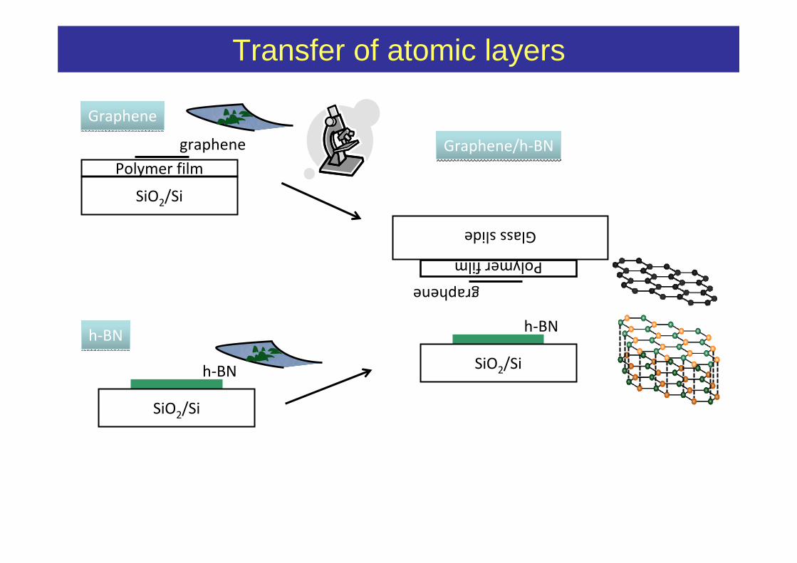
Transfer of atomic layers
graphene
SiO2/Si
Polymer film
graphenePolymer film
GrapheneGraphene
Graphene/h‐BNGraphene/h‐BN
Glass slideh‐BN
SiO2/Sih‐BNh‐BN
h‐BN
SiO2/Si

Graphene on SiO2
SiO2
Si
dangling bond
SiO O
Mobility limited by extrinsic scattering sources
Graphene
Mechanical exfoliation
Surface roughnessDangling bondsCharged impuritySiO2 optical phonon (60 meV)

Graphene on SiO2 v.s. graphene on h-BN
SiO2
Graphene
Si
Hexagonal Boron Nitride Atomically flat surface
Extrinsic scattering sources suppressed
Surface roughnessDangling bondsCharged impuritySiO2 optical phonon (60 meV)
Atomically flat surfaceNo dangling bondsHoneycomb latticeBN optical phonon (100 meV)

BN
TG Graphene
1 m
Graphene
h-BN/SiO2
Back Gate
h-BN
Top Gate
+ + + +
ー ー ー
+ +ー ー
ー
nnn
ppppnp
npn
局所キャリア変調
1.6 K
h-BN / Graphene /h-BN
~ 105 cm2/Vs@RT
Graphene
h-BN/SiO2
Back Gate
h-BN
Top Gate
+ + + +
ー ー ー
+ +ー ー
ー
局所キャリア変調h-BN / Graphene /h-BN
~ 105 cm2/Vs@RT
500 nm
p nn
High quality graphene n-p-n junctions (L > 500 nm)
T = 1.6 K
R (k
)
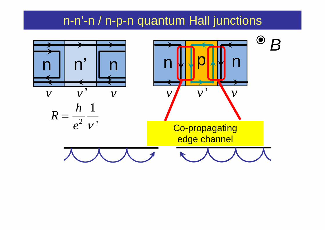
n-n’-n / n-p-n quantum Hall junctions
n p nn n’ nv v’ v
B
v v’ v
2
1'
hRe
Co-propagating edge channel
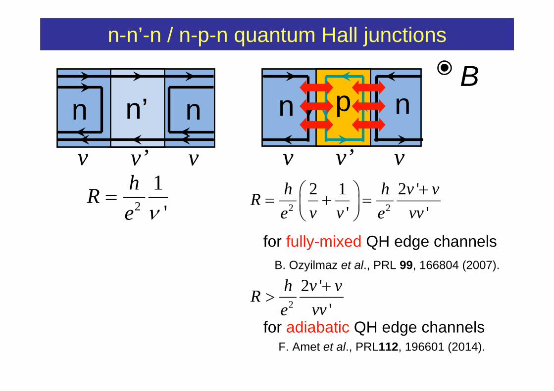
n-n’-n / n-p-n quantum Hall junctions
n pB
v v’ v
n n’ nv v’ v
2
1'
hRe
2 2
2 1 2 '' '
h h v vRv v vve e
for fully-mixed QH edge channelsB. Ozyilmaz et al., PRL 99, 166804 (2007).
for adiabatic QH edge channelsF. Amet et al., PRL112, 196601 (2014).
n
2
2 ''
h v vRvve
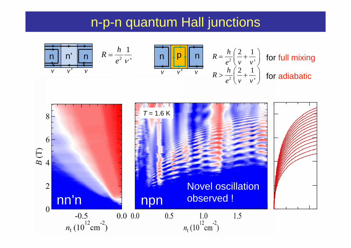
n-p-n quantum Hall junctions
2
1'
hRe
nn’n
2
1'
hRe
n n’ nv v’ v
for full mixing2
2 1'
hRv ve
n p n
v v’ v for adiabatic2
2 1'
hRv ve
Novel oscillation observed !npn
T = 1.6 K

n-p-n quantum Hall junctions
T = 1.6 K
12 21.7 10 cm
12 21.5 10 cm
12 21.3 10 cm
12 21.1 10 cm
12 20.9 10 cm
12 20.7 10 cm
12 20.5 10 cm
12 20.3 10 cm
B ~ 0.5 T
Aharonov-Bohm effect
1hBe S
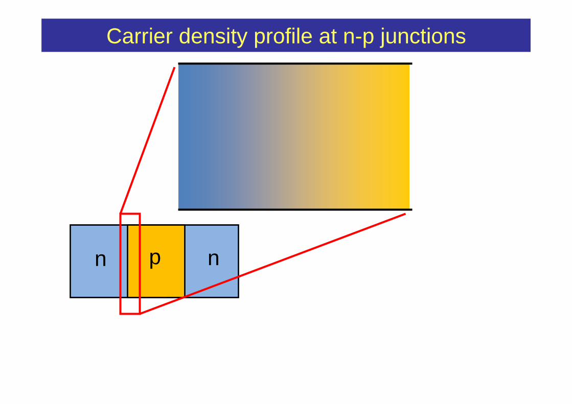
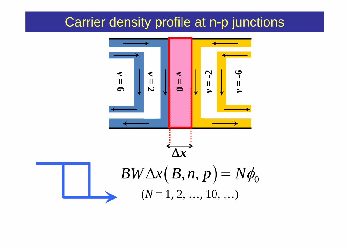
Carrier density profile at n-p junctions
n p n

Carrier density profile at n-p junctions
v= 6 v
= -6v
= 0 v=
-2v
= 2
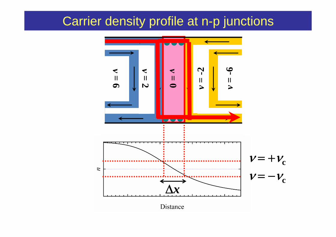
Carrier density profile at n-p junctions
v= 6 v
= -6v
= 0 v=
-2v
= 2
●●●
●●●
x
c
c

= 0 incompressible strip
S
B
S
|nTG|B
B B 1hB
e S 1hB
e S
|nTG|

Local carrier density profile by FEM analysis
Graphene
h-BN/SiO2
Back Gate
h-BN
Top Gate
Graphene
h-BN/SiO2
Back Gate
h-BN
Top Gate
Finite element method(Infolytica Elecnet)
-2
0
2
n (1
012cm
-2)
-100 -50 0 50 100
6
4
2
0
x
(nm
)
86420B (T)
012 2
12 2
12 2
12 2
12 2
12 2
12 2
1.7 10 cm1.5 10 cm1.3 10 cm1.1 10 cm0.9 10 cm0.7 10 cm0.5 10 cm
p
c 0.4
x (nm)
012 2
12 2
12 2
12 2
12 2
12 2
12 2
0.5 10 cm0.7 10 cm0.9 10 cm1.1 10 cm1.3 10 cm1.5 10 cm1.7 10 cm
p
Carrier density profile at n-p junctions
0, ,BW x B n p N (N = 1, 2, …, 10, …)
v= 6 v
= -6v
= 0 v=
-2v
= 2
x

Resistance oscillations
0, ,BW x B n p N
x
v= 6 v
= -6v
= 0 v=
-2v= 2
v= 6 v
= -6v
= 0 v=
-2v= 2 W
(N = 1, 2, …, 10, …)
N = 4
N = 20

Resistance oscillations
x
v= 6 v
= -6v
= 0 v=
-2v= 2
v= 6 v
= -6v
= 0 v=
-2v= 2 W
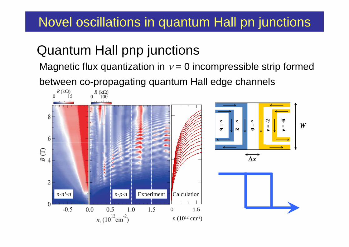
Novel oscillations in quantum Hall pn junctions
Quantum Hall pnp junctions Magnetic flux quantization in = 0 incompressible strip formed between co-propagating quantum Hall edge channels
0 1.5
n (1012 cm-2)
CalculationExperimentn-p-nn-n’-n
x
v= 6 v
= -6v= 0 v
= -2v= 2
v= 6 v
= -6v= 0 v
= -2v= 2 W
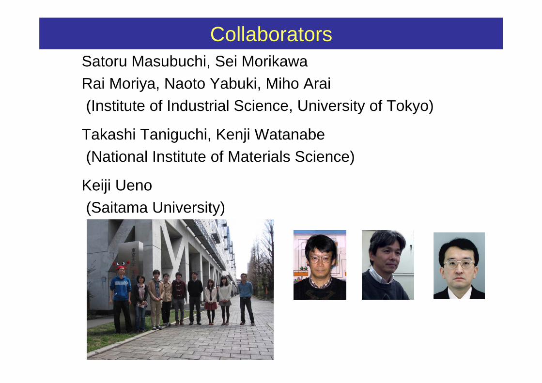
CollaboratorsSatoru Masubuchi, Sei MorikawaRai Moriya, Naoto Yabuki, Miho Arai(Institute of Industrial Science, University of Tokyo)
Takashi Taniguchi, Kenji Watanabe(National Institute of Materials Science)
Keiji Ueno(Saitama University)
SummaryTransfer technique of atomic layersQuantum Hall pnp junctions
Novel magnetoresistance oscillationsCoherent interference in QH edge channels
Graphene/h-BN
Josephson junctionsSupercurrentFraunhofer pattern and Fiske resonance
NbSe2/NbSe2
Magnetic tunnel junctionsMagnetoresistance effect
Fe0.25TaS2/Fe0.25TaS2