quasi continuous wave laser sintering of si-ge ... · sige thin films have high electrical...
TRANSCRIPT

Quasi continuous wave laser sintering of Si-Ge nanoparticles for thermoelectricsKai Xie, Kelsey Mork, Jacob T. Held, K. Andre Mkhoyan, Uwe Kortshagen, and Mool C. Gupta
Citation: Journal of Applied Physics 123, 094301 (2018); doi: 10.1063/1.5018337View online: https://doi.org/10.1063/1.5018337View Table of Contents: http://aip.scitation.org/toc/jap/123/9Published by the American Institute of Physics
Articles you may be interested inUltrahigh thermal conductivity of isotopically enriched siliconJournal of Applied Physics 123, 095112 (2018); 10.1063/1.5017778
Perspective: Acoustic metamaterials in transitionJournal of Applied Physics 123, 090901 (2018); 10.1063/1.5007682
Dual-wavelength GaSb-based mid infrared photonic crystal surface emitting lasersJournal of Applied Physics 123, 093102 (2018); 10.1063/1.5012113
Effect of thermal annealing on the redistribution of alkali metals in Cu(In,Ga)Se2 solar cells on glass substrateJournal of Applied Physics 123, 093101 (2018); 10.1063/1.5016949
Broadband low-frequency sound isolation by lightweight adaptive metamaterialsJournal of Applied Physics 123, 091705 (2018); 10.1063/1.5011251
Negative magnetization and the sign reversal of exchange bias field in Co(Cr1-xMnx)2O4 (0≤x≤0.6)Journal of Applied Physics 123, 093902 (2018); 10.1063/1.5009404
Quasi continuous wave laser sintering of Si-Ge nanoparticlesfor thermoelectrics
Kai Xie,1 Kelsey Mork,2 Jacob T. Held,3 K. Andre Mkhoyan,3 Uwe Kortshagen,2
and Mool C. Gupta1,a)
1Department of Electrical and Computer Engineering, University of Virginia, Charlottesville 22904, USA2Department of Mechanical Engineering, University of Minnesota, Minnesota 55455, USA3Department of Chemical Engineering and Materials Science, University of Minnesota, Minnesota 55455, USA
(Received 5 December 2017; accepted 13 February 2018; published online 2 March 2018)
Silicon-germanium is an important thermoelectric material for high temperature applications. In this
study, thin films composed of SiGe nanoparticles were synthesized in a plasma reactor and sintered
by a millisecond pulse width, quasi continuous wave, near infrared laser of wavelength 1070 nm. We
demonstrate that laser sintered SiGe thin films have high electrical and low thermal conductivity,
dependent on the surface morphology and dopant concentration. Substrate wetting of laser heating
induced molten SiGe was found to play an important role in the final surface morphology of the
films. Interconnected percolation structures, formed when proper substrate wetting occurs, were
found to be more conductive than the balling structure that formed with insufficient wetting. Laser
power was adjusted to maximize dopant reactivation while still minimizing dopant evaporation.
After optimizing laser sintering process parameters, the best electrical conductivity, thermal
conductivity, and Seebeck coefficient were found to be 70.42 S/cm, 0.84 W/m K, and 133.7 lV/K,
respectively. We demonstrate that laser sintered SiGe thin films have low thermal conductivity
while maintaining good electrical conductivity for high temperature thermoelectric applications.
Published by AIP Publishing. https://doi.org/10.1063/1.5018337
I. INTRODUCTION
Silicon germanium (SiGe) plays an important role in
high temperature thermoelectric devices. Current applications
of SiGe include the Radioisotope Thermoelectric Generators
(RTGs) being used by NASA to convert heat generated from
the decay of radioactive isotopes into electricity on deep
space missions.1 Generating electricity from waste heat using
thermoelectric devices is also an attractive alternative energy
source. For example, thermoelectric materials could be used
in automobiles to harvest waste heat to power electrical sys-
tems in the car, thus improving fuel economy and lowering of
greenhouse gas emission.
One of the major problems with current thermoelectric
systems is the low conversion efficiency. The efficiency of
thermoelectric materials is quantified by a dimensionless fig-
ure of merit, ZT. In order to achieve high ZT, a material
must have a high Seebeck coefficient, high electrical conduc-
tivity, and low thermal conductivity. In recent years, studies
have shown that nanocrystalline materials can have better
figure of merits than their bulk counterparts.2 In nanocrystal-
line materials, phonon scattering is enhanced at grain interfa-
ces, thus reducing the part of the thermal conductivity
contributed by phonons jp.3 The resulting effect being that
the overall thermal conductivity may be reduced without sig-
nificantly affecting the electrical conductivity.
Previous work by NASA found ZT¼ 0.7 at 650 �C (Ref.
4) in bulk SiGe with grain sizes on the order of 1–10 lm;
while an MIT research group, using a bulk material with a
20 nm grain size, found ZT¼ 0.75 at 650 �C for p-type
(maximum ZT¼ 0.95 at 900 �C),5 and ZT¼ 1.05 at 650 �Cfor n-type (maximum ZT¼ 1.3 at 900 �C),6 the highest
recorded SiGe figure of merit. The Field Assisted Sintering
Technique (FAST) was used to make bulk materials with
nano-grain structures in both studies.
Lasers have been proved to be a successful tool for large
scale manufacturing,7 because of their low cost, high effi-
ciency, high throughput, and easy operation. In renewable
energy applications, laser processing was reported to per-
form laser doping,8 laser transferring,9 and laser texturing.10
In this work, thin films made of plasma synthesized Si80Ge20
nanoparticles doped with phosphorous were sintered by a
long pulsed infrared laser. We demonstrate that laser sintered
SiGe thin films have high electrical conductivity and low
thermal conductivity. Also, the impact of surface morphol-
ogy on electrical and thermal conductivity was investigated.
II. EXPERIMENTAL
Hydrogen terminated Si80Ge20 nanocrystals with 5%
nominal phosphorous doping were grown in a capacitively
coupled plasma tube reactor and deposited onto a quartz sub-
strate in porous thin films, as described in previous litera-
ture.11 The average crystallite size, surface morphology,
elemental composition, and distribution were found with
XRD, SEM, TEM, and FTIR, respectively.
To investigate the structure and the degree of alloying of
raw films, SiGe nanocrystals (NCs) were deposited directly
onto carbon-coated copper TEM grids (thin carbon/holey sup-
port) and transferred with less than 30 s of air exposure into an
aberration-corrected FEI Titan G2 60-300 (scanning) transmis-
sion electron microscope (STEM) equipped with a Super-Xa)Electronic mail: [email protected]
0021-8979/2018/123(9)/094301/7/$30.00 Published by AIP Publishing.123, 094301-1
JOURNAL OF APPLIED PHYSICS 123, 094301 (2018)

energy-dispersive X-ray (EDX) detector. High-angle annular
dark field (HAADF) STEM images were acquired at 200 kV
(imaging only) and 60 kV (elemental mapping) with a 25 mrad
convergence semi-angle and an 80 pA beam current. Spatially
resolved STEM-EDX maps of individual particles were
acquired with 350� 350 pixels over a 15� 15 nm2 area with a
pixel dwell time of 3 ls/pixel, acquisition time of 10 min, and
drift correction after every frame. The K-edges of Si, Ge, and
O were background-subtracted and integrated, producing ele-
mental maps. A three-pixel Gaussian blur was applied to the
images shown in Fig. 1 to aid in visualization. The data for
each element were radially averaged around the center of the
particle to obtain the radial map shown in Fig. 1(d).
An infrared long pulse laser of wavelength 1070 nm was
chosen for this study because it can heat a large thickness of
the film, which will provide better sintering uniformity. There
are two major benefits to using a long pulse laser instead of a
short pulse laser. First, the thermal effect of the long pulse
laser lasts longer than the short pulse laser, resulting in a
deeper penetration depth. Additionally, the longer thermal
duration will provide better uniformity. Second, the thermal
effect of the long pulse laser works better as an annealing
method and will improve the film’s crystal structure.
The films were sintered by a quasi-continuous wave
(QCW) laser (IPG photonics YLR-150/1500-QCW-AC) with
a 1070 nm wavelength, a Gaussian profile, and a pulse dura-
tion of 0.1 ms. The peak power of the laser was 1500 W at a
100%�set point, and the pulse repetition rate (PRR) was
between 100 Hz and 1000 Hz, depending on the experiment.
For long pulse and CW lasers, both the peak power and the
average power are important. The heating effect of the laser
was varied by the laser peak power, PRR, pulse width, spot
size, and sample scanning speed. The beam was first reflected
by a mirror before passing through a lens with a focal point
3 cm above the sample. This focal point was chosen to
decrease the laser intensity at the surface of the sample and
increase the area covered by beam scanning. The sample
chamber was mounted beneath the beam on a computer con-
trolled x-y stage, allowing for smooth rastering of the sample.
The sample was covered with a quartz slide to reduce dopant
and film loss and the chamber was pumped down to 10�2 Torr
before being purged with argon gas. Low flow argon gas was
then maintained throughout the sintering process to reduce
oxidation of the sample. A schematic of this experimental
setup is shown in Fig. 2.
The electrical conductivity of the film was measured
using the 4-point probe method. An FEI Quanta 650
Scanning Electron Microscope (SEM) was used to character-
ize the surface morphology. The relationship between the
surface morphology and the electrical conductivity is dis-
cussed in Sec. III.
The thermal conductivity of the thin films was deter-
mined using the 3 omega method,12 as shown in Fig. 3. A
650 nm thick photoresist SU-8 was spin coated onto the film
and thermally cured to serve as the insulation layer. Then,
the silver heater pattern was transferred onto the sample
device and the reference device by photolithography.13 An
alternating current with angular frequency x was applied to
the silver heater. The temperature rise can be described by
the following:
DT ¼ 2dT
dRR
V3x
V1x; (1)
where R is the electrical resistance, RdT/dR is the reciprocal
of the temperature coefficient of resistance (TCR) of the
FIG. 1. Representative STEM-EDX analysis. (a) 60 kV HAADF image of a
5% (nominal) P-doped Si80Ge20 NC, showing spherical geometry and no
obvious elemental segregation. (b) Composite map of Si (green) and Ge
(red). (c) Independent elemental maps of Si, Ge, and O. (d) Radially aver-
aged EDX intensity, confirming a relatively uniform distribution of Si and
Ge throughout the NC as well as the presence of a thin �1 nm oxide layer.
(e) 200 kV HAADF-STEM image of a different cluster of 8–10 nm diameter
spherical NCs, showing single crystal lattice fringes and uniform alloying. FIG. 2. Schematic of the experimental setup used to laser sinter SiGe films.
094301-2 Xie et al. J. Appl. Phys. 123, 094301 (2018)

silver heater, and V1x and V3x are the first and third har-
monic voltage. The temperature rise through the SiGe film
DTf can be derived as follows:13
DTf ¼ DTsample �Psample
PrefDTref ; (2)
where DTsample is the temperature rise in the sample device
and DTref is the temperature rise in the reference device.
Therefore, temperature rise through the SiGe film DTf can
be calculated by subtracting the DTref from DTsample. Psample
and Pref are the thermal powers applied to the sample device
and to the reference device, respectively. In order to simplify
the calculation and minimize the heat loss error, both thermal
powers can be adjusted to the same value. Then, the thermal
conductivity can be derived by the following:
j ¼ Psampletf
LwDT; (3)
where tf is the film thickness, L is the length of the heater,
and w is the width of the heater.
The Seebeck coefficient measurement setup is shown in
Fig. 4. One side of the sample was mounted on the heating
element, and the other side was attached to a heat sink. Two
probes were attached on the film. Different temperature gra-
dients were generated and controlled by the thermal module.
The temperatures of hot/cold side and the thermal voltage
are measured by an Omega datalogger thermometer, and
a Kelsey 2400 Source meter, separately. The results are
recorded using a LabVIEW program.
III. RESULTS AND DISCUSSION
A. Plasma synthesized nanocrystalline SiGe thin filmproperties
The nanocrystals composing the film were found to be
crystalline, spherical, and well alloyed and had an average
crystallite size of 8 nm with a 10%–15% standard deviation
as shown in Fig. 1. Past research on this synthesis method has
found the active dopant levels in the synthesized nanoparticle
films to be lower than the nominal levels with the phospho-
rous dopants included via lattice substitution.14 Minor expo-
sures to air between processing steps resulted in some surface
oxidation of the nanocrystals, as shown in Fig. 1.14
Films were found to be between 3 and 10 lm thick,
depending on the deposition time, uniform on the scale
required for sintering and extremely porous. These thick-
nesses are significantly larger than those of other published
thin film type thermoelectric materials.15–19 Thicker films
may allow for a larger temperature gradient to be obtained
thus increasing the thermovoltage output. The high porosity
of the films combined with the deactivation of charge car-
riers during minor oxidation resulted in immeasurably low
electrical conductivity of the pre-sintered films.14
B. Effects of sintering by a long pulse laser
The high energy imparted to the SiGe films by the long
pulse laser during sintering resulted in the melting of the
films. During the melting and the cooling process that fol-
lowed the constituent elements of the films were reordered.
The relatively lower melting temperature of the germanium
caused it to transition from liquid to solid form before the
silicon. This caused the germanium to segregate out of the
SiGe alloy, forming balls of a germanium rich material in
some cases and webbing patterns of a germanium rich mate-
rial in other cases. This can be seen in the backscattering
SEM images in Fig. 5 where the germanium rich materials
appear whiter than the silicon rich. In addition to modifying
FIG. 3. Schematic of the differential 3 omega measurement setup.
FIG. 4. Schematic of the Seebeck coefficient measurement setup.
FIG. 5. SEM, in back scatter mode, images of the balling structure. The laser
parameters were 225 W peak power, 300 Hz PRR, 0.1 ms pulse width, and
0.5 mm/s scanning speed.
094301-3 Xie et al. J. Appl. Phys. 123, 094301 (2018)

the alloy fraction of the SiGe, the temperature needed to
melt the material far surpasses the melting temperature of
the phosphorous dopant. The high heat could cause one of
two effects; some dopants could evaporate out of the mate-
rial with further increase in absorbed laser energy imparted
to the film causing high loss of dopants. Although the quanti-
tative result of dopant loss was difficult to measure because
of the high porosity, the dopant loss was qualitatively
observed by performing Energy-dispersive X-ray spectros-
copy (EDS) before and after the laser sintering process; alter-
natively, phosphorous atoms that were previously not four
fold substitutionally incorporated into the crystal lattice
could be better incorporated into the lattice structure after
laser processing. This would result in an increase in electri-
cal conductivity due to activated dopant atoms and improved
conductive paths.
In order to understand the processes of dopant reactivation
and dopant loss, several attempts were made to measure the
dopant concentration of post sintered samples. However, the
porosity and rough surface of the samples make it not ideal for
secondary-ion mass spectrometry (SIMS). Meanwhile, the low
concentration of phosphorus is too close to the confidence lim-
its of Energy-dispersive X-ray spectroscopy (EDS) and X-ray
photoelectron spectroscopy (XPS) to get an accurate quantita-
tive measure.
C. Segregation of germanium
A Gaussian beam shape is good for process parameter
optimization in lab experiments because it can sinter the film
with different laser energy densities in one scan. The process
of the germanium segregation can be seen in Figs. 6(a) to
6(d). The figure shows the impact of the Gaussian beam pro-
file and surface morphology variation. It also shows different
surface morphologies after sintering with different laser
energy densities. All figures were taken under SEM back
scatter mode. The brighter parts have a higher average
atomic number, and the darker parts have lower average
atomic number. The thickness of the films is measured at
3–5 lm, which is larger than the penetration depth of SEM
predicted by the Kanaya-Okayama formula.20 Therefore,
brighter areas in the figure show germanium rich regions,
while darker areas show silicon rich regions. Figure 6(d)
shows the film sintered by the peak of Gaussian beam, where
the laser energy density was the highest. The maximum sin-
tering temperature of location (d) was higher than that of
location (a), the edge of the Gaussian beam. When the tem-
perature was relatively low, the germanium phase had a low
viscosity and could only form small islands, as shown in Fig.
6(a). The electrical conductivity was close to that of the raw
film because the islands were separated from each other and
no conductive path was formed. When the temperature
became higher, there were two possibilities. If the germa-
nium rich phases wet the substrate well, a semi-continuous
percolation structure is formed. This structure had high elec-
trical conductivity. This could be because of better con-
nected pathways and limited dopant evaporation. However,
if the germanium rich phases did not wet the substrate well,
the previously mentioned small islands of germanium began
to merge together and formed small balls, as shown in Fig.
6(b). When the laser energy density was even higher, the
small balls began to merge together and formed large
islands, as shown in Figs. 6(c) and 6(d). Meanwhile, the high
processing temperature would result in too much dopant
loss. Lack of a conductive path and too low dopant concen-
tration resulted in a near zero electrical conductivity.
D. Surface morphology and electrical conductivity
Some sintering experiments resulted in the balling struc-
ture as seen in Fig. 4. This surface morphology shows segrega-
tion and discontinuity, resulting in an electrical conductivity
too small to be measured. This could be due to a variety of fac-
tors. Poorly chosen sintering parameters or improper cleaning
of the substrate surface could both cause balling. The quartz
substrate was also a potential cause of this balling structure as
the molten silicon germanium did not wet the quartz well.
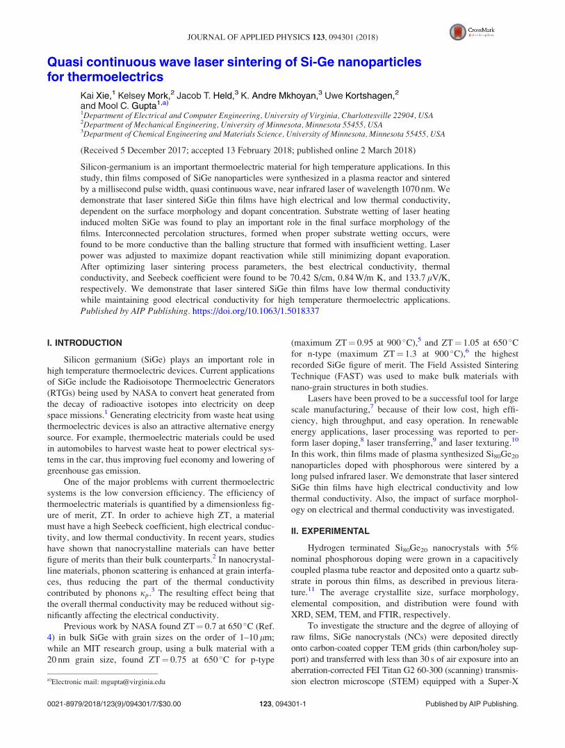
The percolation structure shown in Fig. 7 is a more desir-
able structure. The results shown in Figs. 7(a) to 7(c) were sin-
tered with the same laser peak power of 225 W, the same
scanning speed of 0.5 mm/s, but different PRRs (a) 200 Hz,
(b) 400 Hz, and (c) 800 Hz. The corresponding tilted-view
SEM images are shown on the right. The SEM images were
taken using the back scattering mode that allows for some ele-
mental analysis. The bright parts contain more germanium,
FIG. 6. SEM, in back scatter mode, images of the surface morphology
changes due to the Gaussian beam profile. Brighter areas show germanium
rich regions, while darker areas show silicon rich regions. (a) shows the
films sintered by the edge of the Gaussian beam, with (b)–(c) approaching
the center of the beam and (d) showing the film sintered by the center of
the Gaussian beam. The incident Gaussian beam power profile is plotted at
the top.
094301-4 Xie et al. J. Appl. Phys. 123, 094301 (2018)
while the dark parts contain more silicon. Figures 7(a) and
7(c) have much lower electrical conductivities when com-
pared with Fig. 7(b) but the mechanisms are very different.
Figure 7(a) shows the balling structure beginning to appear
because of bad substrate wetting. In Fig. 7(c), the surface mor-
phology shows that the laser intensity was too high, resulting
in elemental segregation and accumulations of germanium.
Although the conductive regions are still interconnected,
there are fewer conductive paths and they are narrower than
those in Fig. 7(b). Thus, the electrical conductivity of (c) was
lower than that of (b). Figure 7(b) shows the best surface
morphology as well as the best electrical conductivity
because of selection of proper laser parameters. The nanopar-
ticles were interconnected and the surface was more uniform.
The process temperature was also high enough to reactivate
dopant atoms. The best electrical conductivity found in this
study was 70.42 S/cm.
E. Seebeck coefficient, thermal conductivity,and figure of merit ZT
The Seebeck coefficient was measured at room tempera-
ture. The temperature at the hot side of the sample was var-
ied from 301 K to 310 K, and the cold side was held at
300 K, which gives a temperature difference from 1 K to
10 K. At least two heating-cooling cycles were performed to
improve the measurement accuracy. The Seebeck coefficient
of the post sintered films was 133.7 lV/K, compared to
140 lV/K before sintering. The Seebeck coefficient is pri-
marily determined by the composition of the film.15 The
Seebeck coefficient in this study is on the same order of
magnitude compared with other published works.4,6,13,15,21
The thermal conductivity was calculated using Eq. (3).
The effective thermal conductivity of the champion thin film
was calculated to be 0.84 W/m K, which is significantly
lower than the previously reported 2.5 W/m K in 2008 (Ref.
16) and 4.5 W/m K in the bulk RTGs used by NASA.5 The
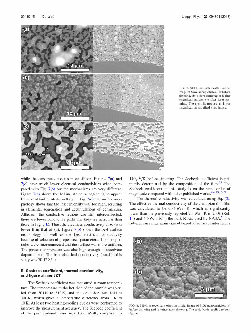
sub-micron range grain size obtained after laser sintering, as
FIG. 7. SEM, in back scatter mode,
image of SiGe nanoparticles, (a) before
sintering, (b) before sintering at higher
magnification, and (c) after laser sin-
tering. The right figures are at lower
magnification and tilted-view image.
FIG. 8. SEM, in secondary electron mode, image of SiGe nanoparticles, (a)
before sintering and (b) after laser sintering. The scale bar is applied to both
figures.
094301-5 Xie et al. J. Appl. Phys. 123, 094301 (2018)

shown in Fig. 8, and the high porosity of these films both
contribute to the low thermal conductivity value.
For our champion device, the figure of merit ZT can be
calculated from the electrical conductivity 70.42 S/cm, effec-
tive thermal conductivity 0.84 W/m K, and the Seebeck coef-
ficient 133.7 lV/K. With ZT ¼ rS2
j T, the figure of merit of
the champion thin film at room temperature is 0.05. This
number is comparable to other published works,4,6,13,15,21
which is from 0.01–0.06. This result suggests that laser sin-
tering provides an easy and economical way to synthesize
thermoelectric materials compared to more expensive and
time-consuming methods like FAST and Low Pressure
Chemical Vapor Deposition (LPCVD).
F. Discussion
Table I compares the results of this work with the ther-
moelectric properties of bulk and thin films SiGe reported by
other researchers. The electrical conductivity of SiGe thin
films is about 1 order of magnitude smaller than that of bulk
SiGe. An important factor that may impact the electrical con-
ductivity is the porosity.21 The Field assisted sintering tech-
nique (FAST) for bulk SiGe synthesis involves mechanical
pressure. Therefore, the porosity of bulk SiGe is usually
much smaller than for thin films. On the other hand, the
effective thermal conductivity will benefit from high poros-
ity. The laser sintering process results in more porous sam-
ples when compared with Low Pressure Chemical Vapor
Deposition (LPCVD). Therefore, laser sintering results in the
smallest thermal conductivity.
In this work, the best electrical conductivity achieved
was 70.42 S/cm, the effective thermal conductivity was
0.84 W/m K, and the Seebeck coefficient was 133.7 lV/K.
The thermal conductivity is significantly lower than the
reported data shown in Table I, excepting the sample with a
film thickness in the nanometer range. The electrical conduc-
tivity could be improved by starting with a less porous and
smoother film. However, a less porous and smoother film
may also enhance the thermal conductivity, and thus lead to
a lowering of figure of merit ZT. Therefore, it is important to
find a balance between thermal conductivity and electrical
conductivity. The figure of merit of the laser sintered SiGe
films in this study was better than that reported with the
same Si80Ge20 ratio, and is only slightly lower than that of
higher germanium content films.17 However, with the cost of
germanium significantly higher than that of silicon, Si80Ge20
would be more desirable in large scale manufacturing.
It is worth mentioning that the method reported in this
paper is suitable for manufacturing applications, because of
the following unique advantages: (1) The overall size of the
sample in this method is not limited by the pressure chamber
as used in FAST; (2) The laser sintering is performed in
atmospheric pressure with no vacuum requirement; (3) No
wet chemical process is required; (4) The overall throughput
is much higher than FAST; (5) Both raw film preparation
and laser sintering can be adapted to be “printing” processes,
which are suitable for automated production.
IV. CONCLUSION
We have demonstrated that the laser sintering is a versa-
tile method in fabricating SiGe thin films for thermoelectric
applications. The laser peak energy, scanning speed, and
PRR were optimized to maximize electrical conductivity and
minimize thermal conductivity. In this study, the best electri-
cal conductivity achieved was 70.42 S/cm, the lowest ther-
mal conductivity was 0.84 W/m K, and the Seebeck
coefficient was 133.7 lV/K. The electrical conductivity was
highly dependent on two major factors. The first factor was
surface morphology. Interconnected percolation structures
provided better conductive pathways, while balling struc-
tures resulted in electrical isolation. The second factor was
dopant reactivation. Dopant atoms can get reactivated during
laser sintering, but the evaporation under high temperature
needs to be minimized. Thermal conductivity was found to
be dramatically reduced by sub-micron grain sizes and high
porosity. The overall process provides a fast, low cost, and
easy way for SiGe thermoelectric thin film fabrication. The
electrical conductivity of laser sintered SiGe films can be
further improved by decreasing the porosity and increasing
TABLE I. Comparison of thermoelectric data for bulk and thin film SiGe.
References Materials Method Doping Type Seebeck lV/K r S/cm j W/m K TK ZT Note
This work Si80Ge20 Laser sintering n Film 133.7 70.42 0.83 300 0.05 a
17 Si70Ge30 LPCVD p Film 131 346 4.7 300 0.04 a
17 Si70Ge30 LPCVD n Film 179 342 5.1 300 0.06 a
18 Si70Ge30 LPCVD p Film 35 909 3.5 300 0.01 a
18 Si70Ge30 LPCVD n Film 190 161 3.5 300 0.05 a
19 Si80Ge20 LPCVD p Film 220 30 2.9 300 0.02 a
15, 22, 23 Si78Ge22 Laser sintering n Film 160–180 15 0.05 300 b
6 RTG Bulk 100–120 1200 4.5 300 0.09 ZT ¼ 0.9 at 1200 K
6 Si80Ge20 FAST n Bulk 100–120 625–825 2.5 300 0.1 ZT ¼ 1.3 at 1200 K
5 Si80Ge20 FAST p Bulk 110–130 800–900 2.25–2.6 300 0.15 ZT ¼ 1 at 1100 K
24 SiGe FAST n Bulk 80–130 900–1650 3.9–6.25 300 0.06 ZT ¼ 1.3 at 1200 K
21 SiGe FAST n Bulk 104 1140 3.94 300 0.09 a
4 Si80Ge20 FAST n Bulk 175 140 1.8 300 0.07 ZT ¼ 0.8 at 1300 K
aNo high temperature data.bNot measured for the same sample.
094301-6 Xie et al. J. Appl. Phys. 123, 094301 (2018)
the dopant concentration, which in turn could further
improve the figure of merit.
ACKNOWLEDGMENTS
We acknowledge R. Skinner (University of Minnesota)
for synthesizing the raw films. We acknowledge the support
of NSF under the Award No. ECCS-1408443. JTH was
supported by the MRSEC program of the National Science
Foundation under Award DMR-1420013. STEM analysis
was performed in the College of Science and Engineering
Characterization Facility of the University of Minnesota,
which receives partial support from the NSF through the
MRSEC program.
1C. Wood, Rep. Prog. Phys. 51, 459 (1988).2G. A. Slack and M. A. Hussain, J. Appl. Phys. 70, 2694 (1991).3G. Pernot, M. Stoffel, I. Savic, F. Pezzoli, P. Chen, G. Savelli, A. Jacquot,
J. Schumann, U. Denker, and I. M€onch, Nat. Mater. 9, 491 (2010).4N. Stein, N. Petermann, R. Theissmann, G. Schierning, R. Schmechel, and
H. Wiggers, J. Mater. Res. 26, 1872 (2011).5G. Joshi, H. Lee, Y. Lan, X. Wang, G. Zhu, D. Wang, R. W. Gould, D. C.
Cuff, M. Y. Tang, M. S. Dresselhaus, G. Chen, and Z. Ren, Nano Lett. 8,
4670 (2008).6X. W. Wang, H. Lee, Y. C. Lan, G. H. Zhu, G. Joshi, D. Z. Wang, J.
Yang, A. J. Muto, M. Y. Tang, J. Klatsky, S. Song, M. S. Dresselhaus, G.
Chen, and Z. F. Ren, Appl. Phys. Lett. 93, 193121 (2008).7M. C. Gupta and D. E. Carlson, MRS Energy & Sustainability 2, 2 (2015).8K. Sun, Y. Bao, and M. C. Gupta, Laser Doping of Germanium forPhotodetector Applications (International Society for Optics and
Photonics, 2014), p. 918008.
9L. Wang, D. E. Carlson, and M. C. Gupta, Prog. Photovoltaics 23, 61
(2015).10P. O. Caffrey and M. C. Gupta, Appl. Surf. Sci. 314, 40 (2014).11D. J. Rowe and U. R. Kortshagen, APL Mater. 2, 022104 (2014).12D. G. Cahill, Rev. Sci. Instrum. 61, 802 (1990).13A. J. Zhou, W. H. Wang, B. Yang, J. Z. Li, and Q. Zhao, Appl. Therm.
Eng. 98, 683 (2016).14N. J. Kramer, K. S. Schramke, and U. R. Kortshagen, Nano Lett. 15, 5597
(2015).15B. Stoib, T. Langmann, S. Matich, T. Antesberger, N. Stein, S.
Angst, N. Petermann, R. Schmechel, G. Schierning, D. E. Wolf, H.
Wiggers, M. Stutzmann, and M. S. Brandt, Appl. Phys. Lett. 100,
231907 (2012).16R. Cheaito, J. C. Duda, T. E. Beechem, K. Hattar, J. F. Ihlefeld, D. L.
Medlin, M. A. Rodriguez, M. J. Campion, E. S. Piekos, and P. E. Hopkins,
Phys. Rev. Lett. 109, 195901 (2012).17J. Xie, C. Lee, M. F. Wang, Y. H. Liu, and H. H. Feng, J. Micromech.
Microeng. 19, 125029 (2009).18Z. Y. Wang, P. Fiorini, V. Leonov, and C. Van Hoof, J. Micromech.
Microeng. 19, 094011 (2009).19M. Takashiri, T. Borca-Tasciuc, A. Jacquot, K. Miyazaki, and G. Chen,
J. Appl. Phys. 100, 054315 (2006).20K. Kanaya and S. Okayama, J. Phys. D: Appl. Phys. 5, 43 (1972).21H. Lee, D. Wang, W. Wang, Z. Ren, B. Klotz, M. Y. Tang, R. Yang, P.
Gogna, J.-P. Fleuiral, and M. S. Dresselhaus, Thermoelectric Properties ofSi/Ge Nano-Composite (IEEE, 2005), p. 269.
22G. Schierning, J. Stoetzel, R. Chavez, V. Kessler, J. Hall, R. Schmechel,
T. Schneider, N. Petermann, H. Wiggers, S. Angst, D. E. Wolf, B. Stoib,
A. Greppmair, M. Stutzmann, and M. S. Brandt, Phys. Status Solidi A
213, 497 (2016).23B. Stoib, S. Filser, N. Petermann, H. Wiggers, M. Stutzmann, and M. S.
Brandt, Appl. Phys. Lett. 104, 161907 (2014).24B. Yu, M. Zebarjadi, H. Wang, K. Lukas, H. Wang, D. Wang, C. Opeil,
M. Dresselhaus, G. Chen, and Z. Ren, Nano Lett. 12, 2077 (2012).
094301-7 Xie et al. J. Appl. Phys. 123, 094301 (2018)