search.jsp?r=19960054089 2018-07-15t20:48:15+00:00z · siegfried w. janson, mechanics and materials...
TRANSCRIPT
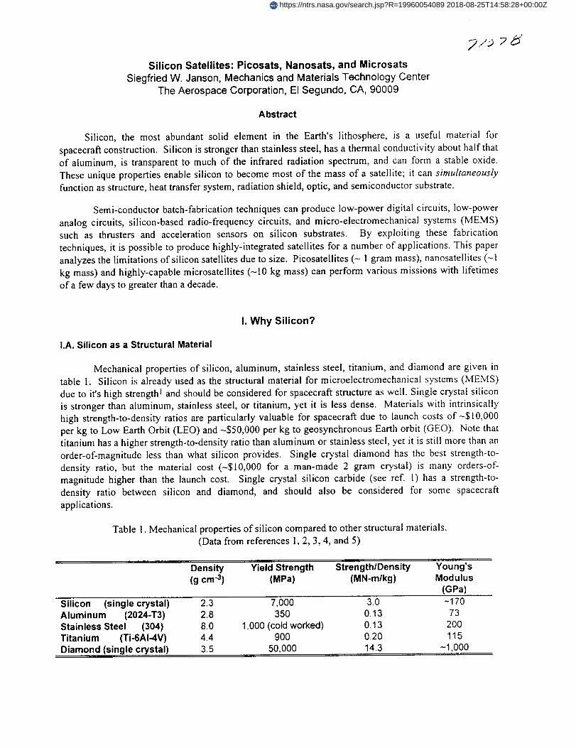
Silicon Satellites: Picosats, Nanosats, and Microsats
Siegfried W. Janson, Mechanics and Materials Technology CenterThe Aerospace Corporation, El Segundo, CA, 90009
Abstract
Silicon, the most abundant solid element in the Earth's lithosphere, is a useful material for
spacecraft construction. Silicon is stronger than stainless steel, has a thermal conductivity about half that
of aluminum, is transparent to much of the infrared radiation spectrum, and can form a stable oxide.
These unique properties enable silicon to become most of the mass of a satellite; it can simultaneouslyfunction as structure, heat transfer system, radiation shield, optic, and semiconductor substrate.
Semi-conductor batch-fabrication techniques can produce low-power digital circuits, low-power
analog circuits, silicon-based radio-frequency circuits, and micro-electromechanical systems (MEMS)such as thrusters and acceleration sensors on silicon substrates. By exploiting these fabrication
techniques, it is possible to produce highly-integrated satellites for a number of applications. This paper
analyzes the limitations of silicon satellites due to size. Picosatellites (- 1 gram mass), nanosatellites (-1
kg mass) and highly-capable microsatellites (-10 kg mass) can perform various missions with lifetimes
of a few days to greater than a decade.
I. Why Silicon?
I.A. Silicon as a Structural Material
Mechanical properties of silicon, aluminum, stainless steel, titanium, and diamond are given in
table 1. Silicon is already used as the structural material for microelectromechanical systems (MEMS)
due to it's high strength I and should be considered for spacecraft structure as well. Single crystal silicon
is stronger than aluminum, stainless steel, or titanium, yet it is less dense. Materials with intrinsically
high strength-to-density ratios are particularly valuable for spacecraft due to launch costs of-$10,000
per kg to Low Earth Orbit (LEO) and -$50,000 per kg to geosynchronous Earth orbit (GEO). Note that
titanium has a higher strength-to-density ratio than aluminum or stainless steel, yet it is still more than an
order-of-magnitude less than what silicon provides. Single crystal diamond has the best strength-to-
density ratio, but the material cost (-$10,000 for a man-made 2 gram crystal) is many orders-of-
magnitude higher than the launch cost. Single crystal silicon carbide (see ref. I) has a strength-to-
density ratio between silicon and diamond, and should also be considered for some spacecraft
applications.
Table 1. Mechanical properties of silicon compared to other structural materials.
(Data from references 1, 2, 3, 4, and 5)
Density Yield Strength Strength/Density(g cm -3) (MPa) (MN-mlkg)
Young'sModulus
(GPa)
Silicon (single crystal)Aluminum (2024-T3)Stainless Steel (304)Titanium (Ti-6AI-4V)Diamond (single crystal)
2.3 7,000 3.02.8 350 O.138.0 1,000 (cold worked) 0.134.4 900 0.203.5 50,000 14.3
-17073
2OO115
~1,000
https://ntrs.nasa.gov/search.jsp?R=19960054089 2018-08-25T14:58:28+00:00Z

While metals are available in a variety of shapes and sizes, single crystal silicon is available in
10, 12.5, 15, and 20 cm diameter cylinders up to 2 meters long. Present manufacturing costs are about
$185 per kg which could drop to -$50 per kg by adopting new refinement techniques. 6 Even though the
material cost (per kg) of single crystal silicon is much more expensive than typical spacecraft structural
materials, it is still more than an order-of-magnitude less than the launch cost. Silicon is a viable
structural material, especially for small satellites.
Thermal properties of silicon, aluminum, stainless steel, titanium, and diamond are given in table
2. Silicon has a high specific heat and a much higher melting point than aluminum. Silicon is a very
good heat conductor; it has a higher thermal conductivity than stainless steel and titanium, and about
50% that of aluminum. Silicon also has a thermal expansion coefficient that is -4 times lower than
titanium and about an order-of-magnitude lower than aluminum and stainless steel. Once again,
diamond has superior properties, but it must be used sparingly due to its high cost.
Table 2. Thermal properties of silicon compared to other structural materials. Specific heat, thermal
conductivity, and thermal expansion coefficient at 300 K.
Thermal Thermal Expansion MeltingConductivity Coefficient Temperature
(Wire OK) (cm/cm OK) (K)Silicon (single crys.) 150 2.5 x 10⁻⁶ 1700Aluminum (2024-T3) 240 2.2 x 10⁻⁵ -850Stainless Steel (304) 16 1.7 x 10⁻⁵ -1700Titanium (Ti-6AI-4V) 8 9 x 10⁻⁶ -2100Diamond (single crys.) 2,100 1.0 x 10⁻⁶ 4200
I.B. Silicon as an Optical Material
Silicon can be used as an optical material throughout most of the infrared spectrum. As shown
in figure 1, it is transparent between 1.4 and 7 microns (wavelength) and from 25 to beyond 100 microns.
The maximum transmission of 54% results from the index-of-refraction of-3.5 over this wavelength
range. Index-matching coatings or surface texturing can be used to bring transmission efficiencies close
to 100% over selected ranges of interest.
,00 iiso ] i
! i it]ITransmission 60 I II.- _1 II j I1Jl
(percent) 40 , _1I I /, I._1 /
IIII20 : ]l_lr\ tl/ IIII: IIW ,
0 tit _.ju !111]1 2 5 10 20 50 100
Wavelength (microns)
Figure 1. Optical transmission of silicon in the infrared.

I.C. Silicon as a Substrate for Electronics
Microprocessors, microcontrollers, memory, and other digital integrated circuits (ICs) are batch-
fabricated primarily on silicon wafers. These wafers are cut from larger single crystals which have been
ground into a cylindrical shape. Hundreds of identical devices are fabricated on a single side of a 0.5 to1 mm thick, 10 to 20 cm diameter, silicon wafer which is cut apart to release the individual rectangular
silicon dice. These dice are then mounted in plastic or ceramic carriers which provide hermetic sealing
against the environment, mechanical rigidity, improved heat dissipation, and electrical connections
which can be soldered or plugged into a circuit board.
Almost the entire mass and volume of spacecraft electronic systems is determined by packaging;
i.e. enclosures ("boxes"), connectors, circuit boards, and chip carriers. Multi-chip modules (MCMs)
place multiple electrically-connected die in a single carrier to reduce wasted space and increase active
device area density. MCMs can achieve 10 to 15 times greater IC packaging densities on circuit boards
than conventional single-die packages with greater system performance and reliability at lower cost. 7
The next step in reducing packaging size and mass is to produce wafers with interconnected dice. This
wafer-scale integration eliminates unnecessary dicing, wiring, and packaging.
How much silicon "real estate" (area) is required for typical functions? Silicon die areas
currently range from -0.2 cm 2 for microcontrollers to -2 cm 2 for high end microprocessors. APIC16C71 microcontroller dice is 0.4 cm x 0.5 cm in size s while a PowerPC 604 dice is 1.24 cmx 1.58
cm. 9 Dynamic random access memory (DRAM) die, suitable for use with microcontrollers and
microprocessors, require -0.03 cm 2 of silicon per million bits of storage capacity. Feature sizes are
steadily decreasing with time and high-end integrated circuits are becoming more complex. Projections
of dice size for DRAMs and high-end microprocessors over the next 15 years, given in table 3, show the
interesting result that dice size for these products is expected to increase with time. By the year 2010,
high-end microprocessor and DRAM dice could be several cm on a side. To support efficient packing of
rectangular dice on circular silicon wafers during fabrication, 30 cm diameter and larger silicon waferswill become common.
Table 3. Roadmap projections for semiconductor technology. (From reference 10)
Year
Smallest Dynamic RAM: Dynamic RAM: Microprocessors: Microprocessors:Feature Dice Size Billions of Bits Dice Size Millions of
(_tm) (cm2) per Dice (cm2) Transistors per cm21995 0.35 1.9 0.064 2.5 41998 0.25 2.8 0.256 3.0 72001 0.18 4.2 1 3.6 132004 0.13 6.4 4 4.3 252007 0.10 9.6 16 5.2 502010 0.07 14.0 64 6.2 90
A single -4 cm x 4cm DRAM dice in the year 2010 could hold 8 gigabytes of information; more
capacity than is currently available on CD-ROMs and most personal computer hard disk drives. A single
DRAM could hold an uncompressed I000 km x 400 km image with 10-meter spatial resolution and 16
bits of intensity resolution. The command and data handling (C&DH) system for a future satellite couldreside in I or 2 dice and fit on a 10 cm diameter wafer with extra silicon area for communications
systems, power controllers, etc.. If circuit complexity remains fixed, circa 2010 dice could be much
smaller than today's versions due to a factor of 5 reduction in feature size. A future microcontroller

equivalentto thePIC16C71,for example,wouldfit onadicesmallerthan 1 mm on a side. The total
silicon area required for the C&DH system in a current generation microsatellite would shrink from - 2cm z to - 0.1 cm 2.
Microprocessors and microcontrollers have been steadily increasing in performance due to
increases in operating speed, partially enabled by smaller feature sizes, and improvements in processing
architectures. Microprocessor clock speeds were a few MHz during the early 1970's, are in the low 100
MHz range today, and are expected to reach the GHz range by 2010. The INTEL 8086 microprocessor,
introduced in 1978, had a 0.33 million-instructions-per-second (MIPS) performance with a 5 MHz clock
speed while the INTEL Pentium, introduced in 1993, had a 112 MIPS performance with a 66 MHz clock
speed. II By extrapolating the exponential performance increases in microprocessors over the last 15
years (about a 1.5 times increase in performance per year), the predicted performance by 2010 is 100,000
MIPS. This is quite staggering when one realizes that NASA's Galileo probe uses a mere 0.5 MIPS
processor for C&DH.
While silicon has been the substrate of choice for commercial digital circuits, operating
frequencies of-1 GHz and higher will require special wafers or another substrate such as gallium-
arsenide. Currently, silicon offers lower cost and simplified power requirements while gallium arsenide
offers higher frequency operation and higher efficiency. A comparison of silicon and gallium-arsenide
transistor circuits is given in table 4. The gallium arsenide cost in table 4 is based on a total
manufacturing cost of $1500 per 10 cm diameter wafer with a 75% yield, t2
Table 4. Basic comparison between gallium-arsenide and silicon transistor integrated circuits. Datafrom reference 12.
ParameterCost per mm 2
Cutoff frequencyBreakdown VoltageSubstrate
Noise figure @ 5 GHzBias requirementsPower added efficiency
Gallium-Arsenide MESFET
$0.25 (10 cm diameter wafer)18 to 25 GHz15 to 20 V
Insulating1.5 dB
positive and negative6O%
Silicon Bipolar$0.10 (20 cm diameter wafer)12 to 18 GHz5to9VConductive6.0 dB
positive4O%
While data processing circuits may not yet run at GHz clock speeds, satellite communications
circuits routinely operate from -100 MHz to greater than 20 GHz. Below -1 GHz, conventional CMOS
technologies on conventional silicon wafers can provide inexpensive radio-frequency integrated circuits.
One group at UCLA is investigating 2-chip and single-chip fully-integrated (rf, analog, and digital)CMOS transceivers for operation in the 900 MHz industrial, scientific, and medical (ISM) band. 13 Their
goal is to produce a frequency-hopped spread-spectrum transceiver with up to 160 kilobit/sec data
transfer rates at 20 mW power output and 100 milliampere, 3 Volt DC input, t4
Above 1 GHz, gallium arsenide offers increased DC-to-RF conversion efficiency for power
amplifiers and decreased noise for preamplifiers (low noise amplifiers at the receive antenna) used in
communications systems. Standard silicon microwave monolithic integrated circuits (MMICs) usually
perform poorly above a few GHz because commercial wafers have a resistivity on the order of 10 f'2-cm,
whichis too lowtoactasagooddielectric.15Betterperformancecanbeachievedusinghigh-resistivitysiliconsubstrates(10,000f2-cmandhigherfor up to 40GHzoperation)or silicon-on-insulator(SOl)construction.A morerecentdevelopmentis silicon-germanium(SiGe)technologythatoffershigherthan70GHzoperationonsiliconsubstrates.16,17Today'ssilicontechnologycanbeusedfor satellitecommunicationsbandsfromVHF(veryhighfrequency;-140 MHz)to S-band(2.5to 2.7GHz). Futureadvancementsinsilicontechnologywill pushtheoperatingfrequencyrangehigher.
I.D. Silicon as a Radiation Shield
The near-Earth space environment is much harder on electronics than the surface environment
due to the presence of high-energy electrons, protons, and heavier ions. Elastic scattering of high energy
protons and ions results in displacements of stationary target atoms while inelastic scattering results insecondary particle "showers" of lower-energy target atoms or fission daughter products. High-energy
electrons, protons, and ions all leave ionizing tracks behind them. Anomalous effects in semiconductor
circuits due to these interactions range from a temporary change in logic state, due to the sudden
appearance of charge, to permanent substrate atom and charge dislocations which produce altered
current-voltage characteristics and possible device failure, t8 Single-event upsets (SEUs) are particle-
induced "bit-flips" while latchups are more serious high-current flow conditions generated by new low-
resistance paths created by particle-induced ionization trails. Both SEUs and latchups can be controlled
by appropriate choice of semiconductor technology, "watchdog" and error-correction circuits, and error-correction software. Continual accumulation of radiation damage, however, ultimately results in device
failure.
Table 5, adapted from reference 19, gives rough radiation hardness levels for different types ofsemiconductor devices. A rad is the amount of particle radiation that deposits 100 ergs of energy per
gram of target material and the radiation hardness level represents total dose required for device failure.
Typical low-power consumer electronic components (CMOS) are designed to operate in our low-
radiation biosphere (roughly 0.3 rad/year) but can tolerate 1 to 10 kilorad integrated radiation doses.
Unfortunately, the radiation tolerance varies widely from design to design so radiation testing should be
performed on selected components. Transistor-transistor logic (TTL) and emitter-coupled logic (ECL)
circuits are inherently more radiation hard than CMOS, but they require more power. NMOS, PMOS,
I2L, and silicon-on-sapphire MOS circuits can be fully immune to latchup. Radiation hardening requiresa balance between power and circuit availability for choice of technology, mass requirements for
shielding, and circuit complexity for latchup and SEU control.
How much silicon radiation shielding is required for a given mission? Dose rates for a silicon
target are usually given as a function of grams/cm 2 or thickness of spherical aluminum shielding for a
given orbit and given solar conditions (i.e. minimum or maximum solar activity). Silicon and aluminum
are next to each other on the periodic table; their nuclei and average atomic masses differ by only one
proton, and they have similar densities. Both materials have similar ability to slow down incident
energetic electron and protons while silicon generates a slightly higher level of bremsstrahlung X-rays
because bremsstrahlung is proportional to the square of the atomic number (142 for Si vs. 132 for AI).
Aluminum and silicon shielding thicknesses in grams/cm 2 are equivalent within the uncertainties of
radiation environment estimates.

Table5.Radiationhardnesslevelsfor semiconductordevices
Technology Total Dose in rads (silicon)CMOS (soft) 103 - 104
CMOS (hardened) 5 x 10⁴ - 106CMOS (silicon-on-sapphire: soft) 103 - 104
CMOS (silicon-on-sapphire: hardened) > 105ECL 10712L 105 - 4 x 10⁶
Linear integrated circuits 5 x 10³ - 107MNOS 103 - 105
MNOS (hardened) 5 x 10⁵ - 106NMOS 7 x 10² - 7 x 10³PMOS 4 x 10³ - 105TTL/STTL > 106
Figure 2 shows the yearly dose rate due as a function of aluminum shielding thickness (full
sphere shielding) for 700 km altitude orbits with inclinations of 28.50 and 98.2 °. CMOS circuits with an
assumed total radiation dose tolerance of-3000 rads will require at least 0.3 g/cm 2 aluminum (or 1.3 mm
of silicon thickness) shielding for a 1 year on-orbit lifetime in a 700 km, 28.5 ° inclination orbit. For themore interesting sun-synchronous (98.2 ° inclination) orbit, about 0.8 g/cm 2 (or 4 mm silicon thickness)
is required for a 1 year lifetime and about 3 g/cm 2 (1.3 cm silicon) for a 10 year lifetime. At lower
altitudes, significantly less shielding is required, while at higher altitudes, significantly more shielding
may be required. Use of more radiation-resistant technologies is the only solution for some orbits.
Figure 3 shows the dose rate dependence as a function of circular equatorial orbit altitude inside
spherical aluminum shields with densities of 0.5 g/cm 2 (0.18 cm thick aluminum or 0.21 cm thick
silicon) and 3.0 g/cm 2 (1.1 cm thick aluminum or 1.3 cm thick silicon). Note the rapid rise in dose rate
with altitude below 1000 nmi (1850 km), the existence of a hard-to-shield proton belt at -2000 nmi
(3700 km), and the existence of an easier-to-shield electron belt at -10,000 nmi (18,500 km). At
geosynchronous Earth orbit (GEO; 35,786 km or 19,320 nmi altitude and 0 ° inclination) with a
maximum dose of 3,000 rads, 0.5 gm/cm 2 (0.22 cm silicon) and 3.0 gm/cm 2 (1.3 cm silicon) shielding
give lifetimes of roughly 11 days and 3 years, respectively.

10e
10s
Total Dose10'
(Rads/year Si)
103 -
10z0.01
1 I
\
nclination
28.5 ° inclination _
I I "
0.10 1 10
Shielding Thickness (gm I cm 2 Aluminum)
Figure 2: Total yearly dose, under solar maximum conditions, in silicon as a function of aluminum
shielding thickness for 700 km circular orbits. Data adapted from reference 20.
10 e
10 s
Dose Rate
(radslyear [Si])
10 4
10 2
1 i i
Mostly 112g/cm2protons shielding (AI)
Mostlyelectrons
3 g/cm2shielding (AI)
10 2 I I =10 2 10 3 10 4 10 s 10 s
Altitude (nautical miles)
Figure 3. Radiation environment for circular equatorial orbits. (Adapted from ref. 19)

I.E. Silicon as a Substrate for Spacecraft Systems
Microelectro-mechanical systems (MEMS) such as micron-scale silicon diaphragm pressure
sensors, acceleration sensors, chemical sensors, and valves have already been demonstrated.21,22,23, 24
Concepts for silicon-based, batch-fabricated chemical and electric propulsion systems suitable for small
satellites have also been presented. 2s Integration of MEMS with microelectronics for data processing,
memory, signal conditioning, power conditioning, and communications results in a stand-alone
"application-specific integrated microinstrument" (ASIM). Examples of MEMS and ASIM applications
for spacecraft can be found in reference 26 and in other papers from this conference.
II. Silicon Satellites
II.A. Introduction
The silicon satellite, as introduced in references 27 and 28, presented a new paradigm for space
system design, construction, testing, architecture, and deployment. Integrated spacecraft complete with
some degree of attitude and orbit control can be designed for mass-production using batch-fabrication
techniques. Integrated circuits for C&DH, communications, power conversion and control, on-board
sensors, attitude sensors, and attitude control devices can be manufactured on thick silicon substrates that
provide structure, radiation shielding, and thermal control. Some conventional components such as
batteries and individual solar cells will still be required, but the total number of parts and assembly time
will be drastically reduced. The spacecraft, as shown in figure 4, is essentially a muiti-ASIM module.
Solar Cell Wafer
Battery HousingWafer (non-silicon
Solar Cells
Primary MirrorWafer "_
Antenna
Solar Cell Wafer
10 to 15 cm91 ="v
Attitude Determinationand Control Modules
Main Wafer:Computer, ImageSensor, Memory,
Power Conditioning,Internal Sensors,Radio Modems,
Receivers,& Transmitters
Figure 4. A hypothetical silicon satellite.
Silicon wafers are routinely produced with diameters up to 20 cm which will increase to 30 cm
within a decade. Low-volume (10 to 1000 wafers) production of custom circuits and MEMS uses wafers
with diameters less than 15 cm. Simple ASIM-based integrated satellites will have dimensions of 10 to

20 cm while more complex configurations using additional non-silicon mechanical structure (i.e. truss
beams, honeycomb panels and inflatable structures) will be much larger.
The benefits of batch-fabricated silicon satellites are:
1. Reduced parts count due to integrated electronics, sensors, and actuators on a single substrate,
2. The ability to add redundancy and integrated diagnostics without significantly impacting production
cost,
3. Decreased material variability and increased reliability due to rigid process control,
4. Rapid prototype production capability using electronic circuit, sensor, and MEMS design librarieswith existing (and future) CAD/CAM tools and semiconductor foundries,
5. Elimination of labor-intensive assembly steps (welding, wiring cable harnesses, etc.)
6. Automated testing of systems and subsystems, and
7. Paper less documentation of designs, fabrication processes, and testing.
Low cost per function is a direct result of the fabrication process; semiconductor batch
fabrication techniques evolved within the constraints of consumer-driven market economics. Low mass
and volume are simply byproducts of the fabrication process that can be exploited for space applications.
ll.B. Satellite Classification
The term "microsateilite" has traditionally been used for satellites with masses between about
100 kg and 10 kg. Recently, the terms "nanosatellite" and "picosatellite" have been used almost
interchangeably for 1 kg class vehicles. In an attempt to standardize these names and still keep within
the spirit of the prefixes "micro", "nano", etc., I propose a new classification scheme given in table 6.
Table 6. Satellite classification by mass
Classification
Microsatellite
Nanosatellite
Picosatellite
Femtosatellite
Mass Range
1 kg to 100 kg
1 gram to 1 kg
1 milligram to 1 gram
1 microgram to 1 milligram
II.C. Power Considerations
How much solar power can small satellites produce? Assuming that all of the available surface
area is covered by solar cells, the extremes occur for a cubic satellite and for a satellite spread out into a
-10 micron-thick sheet; i.e. a fiat all-solar-array satellite. Figure 5 shows the power extremes for 20%
solar conversion efficiency, random pointing for a cubic satellite, and optimum pointing for a thin sheet
satellite with average density equal to silicon. Picosatellites through microsatellites can produce power
levels in the 1 to 100 Watt range while femtosatellites are in the microwatt to milliwatt range.

v
O(3.
m
Ott}
1E8
1E6
1E4
100
1
0.01
1E-4
1E-61E-6
femto- pico- nano- micro-u_'- _,ql iw..'- _-ql
10 micron-thick sheet
• .
I J I i i
1E-4 0.01 1 100 1E4
Satellite Mass (grams)
1E6
Figure 5. Solar power output ranges, in full on-orbit sunlight, for satellites with an average density equal
to silicon and 20% power conversion efficiency over all exterior surfaces.
ll.D. Thermal Considerations
The overall thermal balance of a spacecraft is determined by its orbit, its geometry, its surface
properties, and its internal design. Solar flux (-1370 W/m 2) has an effective blackbody temperature of5800 K. The Earth reflects -30% of this incoming solar radiation back to space; the average reflectance
or albedo ranges from 23% at the equator to 74% over Antarctica. 29 Over 95% of direct and reflected
solar energy is carried by photons with wavelengths between 0.2 and 2.5 microns. Thermal radiation
from the Earth has an effective blackbody temperature of-300 K which has 98% of the energy carried
by photons with wavelengths greater than 5 microns. The primary energy input to a satellite, averaged
over an orbit, is direct and reflected solar radiation while the primary energy outflow is infrared emission
from the spacecraft at wavelengths greater than 5 microns. The average emissivity (or absorptivity) ct in
the visible and near infrared wavelength range (0.4 to 2 microns) controls the major heat input to
spacecraft surfaces while emissivity e in the medium to long infrared wavelength range (5 to 50 microns)
controls the heat rejection capability of spacecraft surfaces.
At thermal equilibrium, the heat radiated by a satellite to space is just the sum of the energy
absorbed plus heat generated internally:
aA, G, + etA,G_ + eA_G, + Q = e_T4 A, (l)
where A s is the surface area for absorption of solar energy, A e is the surface area for absorption of solar
energy reflected by the Earth, G r is the local flux of sunlight reflected from the Earth, G e is the local flux
of thermal energy radiated by the Earth, Q is the internal heat generation rate, _ is the Stefan-Boltzmannconstant (5.67 x 10"16 W/(m2*T4), T is temperature, and A r is the surface area for heat radiation. As
spacecraft shrink in size, surface-area-to-volume ratios and hence surface-area-to-mass ratios increase.
Small satellites with body-mounted solar arrays can have power-to-mass ratios equivalent to large
satellites with deployable solar arrays, yet still be power-limited. High fractional surface coverage for

solarcellsisgenerallytherule,whichresultsinspacecraftwhosethermalbalanceisdeterminedbysolarcellabsorptivityandemissivity.Thisdoesnotallowmuchlatitudein controllingspacecrafttemperaturerangesfor smallsatellites.
Considerthermalcontrolof a l0 cm diameter,1.2-kgmasssphericalsiliconmicrosatelliteatanaltitudeof 700km. TheIR flux fromtheEarthGe is -200 W/m 2 over the entire orbit and the reflected
solar flux G r is -260 W/m 2 over about half the orbit. If we assume that the surface is completely
covered by 20% efficient solar cells, the orbit average electric power is -1.5 Watts. With an absorptivity
of 0.8 and an emissivity of 0.83, the maximum equilibrium temperature (full sunlight + reflected sunlight
+ Earth IR + internal heat generation) from eq. (1) is 306 K while the minimum equilibrium temperature
(Earth IR + internal heat generation) is 209 K. Conventional spacecraft electronics and batteries cannot
tolerate these temperature extremes. Fortunately, the satellite's thermal mass and appropriate insulation
techniques can be used to control temperature fluctuations for key spacecraft systems.
Figure 6 shows spacecraft temperature, as a function of time, for 4-cm-diameter, 10-cm-
diameter, and 20-cm-diameter solid silicon spheres (nanosatellites and microsatellites) fully covered by
solar cells. Their masses are 80 grams, 1.2 kg, and 9.8 kg, respectively. The orbit is a 700 km altitude
circular equatorial orbit (0 ° inclination) and the solar cells have the same efficiency, emissivity, and
absorptivity used in the previous equilibrium temperature calculations. The dynamic spacecraft
temperature is calculated in one-minute time intervals by numerically integrating a lumped-heat-capacity
energy equation:
(_AsGs+ c_AeGr+ _AeGe + Q-_T4 Ar= d (mc pT) (2)
where d/dt is the first time derivative, m is the spacecraft mass, and cp is the constant-pressure heat
capacity of silicon (736 joules/kg*K). As diameter increases, mass and thermal capacity increase, which
results in reduced temperature swings over an orbit.
305
._. 295
,- 285
275Q.
E
° \_ 265
255
0
Sunlight Eclipse
L I
/"q["-'_ 2 cm radius
A
50 1O0 150
Time (minutes)
200
Figure 6: Spacecraft temperature as a function of time for a solid spherical silicon spacecraft covered
completely by solar cells with absorptivity of 0.8 and emissivity of 0.83. These temperatures were
calculated using a lumped heat-capacity model assuming a circular orbit at an altitude of 700 km.
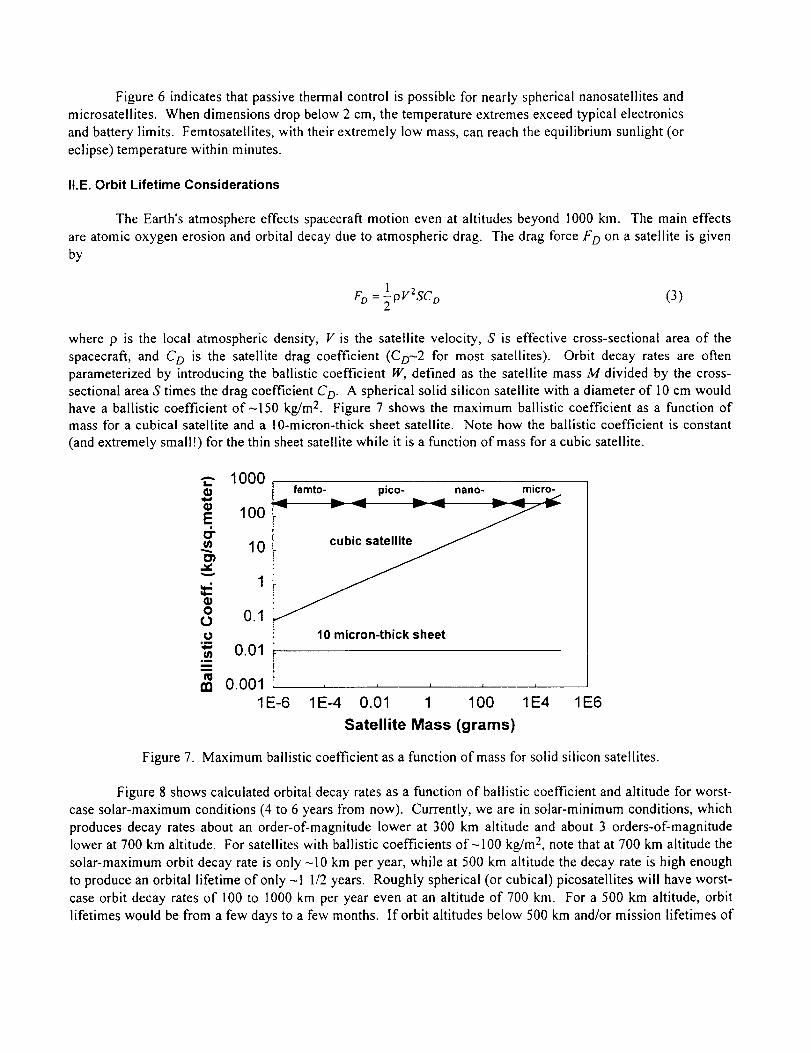
Figure6 indicatesthatpassivethermalcontrolis possiblefor nearlysphericalnanosatellitesandmicrosatellites.Whendimensionsdropbelow2cm,thetemperatureextremesexceedtypicalelectronicsandbatterylimits. Femtosatellites,withtheirextremelylowmass,canreachtheequilibriumsunlight(oreclipse)temperaturewithinminutes.
II.E. Orbit Lifetime Considerations
The Earth's atmosphere effects spacecraft motion even at altitudes beyond 1000 km. The main effects
are atomic oxygen erosion and orbital decay due to atmospheric drag. The drag force F D on a satellite is given
by
Fo = ½0Z2SCo (3)
where p is the local atmospheric density, V is the satellite velocity, S is effective cross-sectional area of the
spacecraft, and CD is the satellite drag coefficient (CD-2 for most satellites). Orbit decay rates are often
parameterized by introducing the ballistic coefficient IV, defined as the satellite mass M divided by the cross-
sectional area S times the drag coefficient CD. A spherical solid silicon satellite with a diameter of 10 cm would
have a ballistic coefficient of-150 kg/m 2. Figure 7 shows the maximum ballistic coefficient as a function ofmass for a cubical satellite and a 10-micron-thick sheet satellite. Note how the ballistic coefficient is constant
(and extremely small!) for the thin sheet satellite while it is a function of mass for a cubic satellite.
--- 1000
Ecr
o00
m
100
10
1
0.1
0.01
0.0011E-6
femto- pico- nano- micro-
10 micron-thick sheet
i i I l
1E-4 0.01 1 100 1E4 1E6
Satellite Mass (grams)
Figure 7. Maximum ballistic coefficient as a function of mass for solid silicon satellites.
Figure 8 shows calculated orbital decay rates as a function of ballistic coefficient and altitude for worst-case solar-maximum conditions (4 to 6 years from now). Currently, we are in solar-minimum conditions, which
produces decay rates about an order-of-magnitude lower at 300 km altitude and about 3 orders-of-magnitude
lower at 700 km altitude. For satellites with ballistic coefficients of-100 kg/m 2, note that at 700 km altitude the
solar-maximum orbit decay rate is only -10 km per year, while at 500 km altitude the decay rate is high enough
to produce an orbital lifetime of only _1 1/2 years. Roughly spherical (or cubical) picosatellites will have worst-
case orbit decay rates of 100 to 1000 km per year even at an altitude of 700 km. For a 500 km altitude, orbit
lifetimes would be from a few days to a few months. If orbit altitudes below 500 km and/or mission lifetimes of

greaterthana few yearsarerequired,dragmake-uppropulsionfor femtosatellitesandpicosatelliteswill bemandatory.
A
t_
E
tY
t3,m
e_L_
O
1000
100
10
I _ 300 kT50 km
400 k50 k
.......0:10 1O0 1000 1 E4
Ballistic Coefficient (kg/m^2)
Fig. 8. Orbit decay rates as a function of ballistic coefficient and altitude for circular orbits under very activesolar conditions.
III. Conclusions
III.A. Femtosatellites and Picosatellites
Femtosatellites don't have enough radiation shielding or a high enough ballistic coefficient to
survive more than a week on-orbit. At altitudes below 500 km where radiation shielding (0.38 mm
maximum for a 1 milligram cubic femtosatellite) may be adequate for radiation-hardened electronics, the
high ballistic coefficient limits lifetimes to a few days. At higher altitudes, rapidly increasing radiation
levels also limit lifetime to a few days. Femtosatellites should be nearly spherical in shape to minimize
air drag and maximize radiation shielding. Maximum power generation levels will therefore be in the
sub-milliwatt range. Active femtosatellites are an extremely difficult challenge due to their low thermalmass and wild temperature swings.
Picosatellites are the smallest useful satellites, but active thermal control will be required. A
thermally passive picosatellite will have temperature swings of 90 K between sunlight and eclipse in low
Earth orbit. Cubic picosatellites can have as much as 0.18 cm silicon radiation shielding and a ballisticcoefficient of-9 kg/m 2. Orbit lifetimes can be several years at 700 km altitude under solar-maximum
conditions and several years at 500 km under solar-minimum conditions. Nearly spherical satellites are
needed to provide radiation shielding, and if low-inclination orbits are used (below 700 km altitude),
radiation-soft CMOS electronics may be feasible. Power outputs will be in the 10's of milliwatts range.Picosatellites may be good for disposable or short-duration (i.e. 1-week) missions.

III.B. Nanosatellites
Nanosatellites are the smallest satellites that don't require active thermal control. Silicon
radiation shielding thicknesses greater than 1 cm are possible with power outputs in the Watt range.
Nearly spherical nanosatellites can operate for several years at altitudes below 500 km in LEO due to
their modest ballistic coefficients, and in GEO due to increased radiation shielding. Flattened
nanosatellites, i.e. 2 cm thick disks, can produce several Watts of solar power and still retain good
thermal control, radiation shielding, and modest ballistic coefficient.
III.B. Microsatellites
Microsatellites have the best power, radiation shielding, orbit lifetime, and thermal
characteristics. Flattened silicon microsatellites offer mission lifetimes of years or decades with power
levels of 10 to 100 Watts.
Acknowledgments
This work was supported by the Technology Development and Applications Directorate of the
Aerospace Corporation. I gratefully acknowledge their support and for previous support provided by the
Aerospace Sponsored Research Program.
References:
I. Kurt E. Petersen, "Silicon as a Mechanical Material," Proceedings of the IEEE, 70 #5, p.420-427, May 1982.
2. ASM Specialty Handbook: Aluminum and Aluminum Alloys, edited by J.R. Davis and Associates, p. 68 - 73,ASM International, Materials Park, Ohio, May 1994.
3. ASM Specialty Handbook: Stainless Steels, edited by J.R. Davis and Associates, p. 7-10, ASM International,
Materials Park, Ohio, Dec. 1994.
4. Metals Handbook Volume 2: Nonferrous Alloys and Special-Purpose Materials, p. 620-622, ASM International,
Materials Park, Ohio, Oct. 1990.
5. ASM Engineering Materials Reference Book; Second Edition, edited by Michael Bauccio, p. 281-282, ASMInternational, Materials Park, Ohio, March 1995.
6. L.C. Rogers, "Chapter 2: Polysilicon Preparation" in Handbook of Semiconductor Silicon Technology, edited by
W.C. O'Mara et al., Noyes Publications, Park Ridge, N J, 1990.
7. Ron Schneiderman, "Multichip Modules Gain Ground at Higher Frequencies," Microwaves and RF, p.49-50,
May 1993.
8. Direct measurement on UV-erasable unit (quartz window shows dice size)
9. Peter H. Singer, "PowerPC 604 in Production," Semiconductor International, p. 17, 17, #11, October 1994.
I0. Linda Geppert, "Technology 1996: Solid State", IEEE Spectrum, 33 #1, p. 51 - 55, January 1996.
1 I. Michael Feibus and Michael Slater, "Pentium Power," PC Magazine, p. 108-120, 12 #8, April 1993.
12. Charles Huang, "GaAs MMIC Power Amplifiers Drive Cellular Systems," Microwaves and RF, p. 85-86,
October 1994.
13. Asad A. Abidi, "Low-Power Radio-Frequency IC's for Portable Communications," Proceedings of the IEEE, 83,
#4, p. 544-569, April 1995.

14.JonathanMinet al.,"AnAII-CMOSArchitecturefor a Low-PowerFrequency-Hopped900MHzSpread-SpectrumTransceiver,"Proceedingsof theIEEECustomIntegratedCircuitsConference,p. 379-382,SanDiego,CA,May1-4,1994.
15.SusanReineckeTaubandSamuelA.Alterovitz,"SiliconTechnologiesAdjustto RFApplications,"p.60-74,MicrowavesandRF,33,#10,October1994.
16.Johann-FriedrichLuyetal.,"Si/SiGeMMICs,"p. 705-714,IEEETransactionsonMicrowaveTheoryandTechniques,43,#4,Aprl1995.
17.G.Daweetal.,"SiGeTechnology:ApplicationtoWirelessDigitalCommunications,"p.14-23,AppliedMicrowaveandWireless,Summer1994.
18.RobertD.Rasmussen,"SpacecraftElectronicsDesignforRadiationTolerance,"ProceedingsoftheIEEE,76#11,p.1527-1537,November1988.
19.MichaelD.GriffinandJamesR.French,Space Vehicle Design, p. 70, American Institute of Aeronautics and
Astronautics, Washington D.C, 1991.
20. Michele M. Gates, Mark J. Lewis, and William Atwell, "Rapid Method of Calculating the Orbital Radiation
Environment," Journal of Spacecraft and Rockets, 29 #5, p. 646-652, Sept.-Oct. 1992.
21. J.B. Angell et al., "Silicon Micromechanical Devices," Scientific American, p.44-55,248, #4, April 1983.
22. R.T. Howe et al., "Silicon Micromechanics: Sensors and Actuators on a Chip," IEEESpectrum, p.29-35, 27,
July 1990.
23. K. Wise and K. Najafi, "Microfabrication Techniques for Integrated Sensors and Microsystems," Science, p.1335-1342, 254, 29 Nov. 1991.
24. M. Mehregany, "Microelectromechanical Systems," IEEE Circuits & Devices, p. 14-22, 9, July 1993.
25. S.W. Janson, "Chemical and Electric Micropropulsion Concepts for Nanosatellites," AIAA Paper 94-2998, 30th
AIAA/ASME/SAE/ASEE Joint Propulsion Conference, Indianapolis, IN, June 1994.
26. S.W. Janson, "Spacecraft As an Assembly of ASIMs," p. 181-258 in Microengineering Technology for Space
Systems, edited by H. Helvajian, Aerospace Technical Report ATR-95(8168)-2, The Aerospace
Corporation, El Segundo, CA, Sept. 1995.
27. S.W. Janson, "Mini-, Micro-, and Nanosatellite Concepts," p. 67 - 75, in Micro- and Nanotechnologyfor
Space Systems. An In#ial Evaluation, edited by H. Helvajian and E. Robinson, Aerospace TechnicalReport ATR-93(8349)-1, The Aerospace Corporation, El Segundo, CA, March 1993.
28. S.W. Janson, H. Helvajian, and E.Y. Robinson, "The Concept of Nanosatellite for Revolutionary Low-Cost
Space Systems," Paper IAF-93-U.5.573, 44th Congress of the International Astronautics Federation, Graz
Austria, October 1993.
29. David G. Galimore, "Satellite Thermal Environments," Chapter 2 in Satellite Thermal Control Handbook, edited
by D.G. Gilmore, The Aerospace Corporation Press, E! Segundo, CA, 1994.
