r8c/36c group datasheet - media.digikey.com sheets/renesas/r8c,36c group.pdf · r8c/36c group 1....
TRANSCRIPT
REJ03B0296-0100 Rev.1.00 Page 1 of 56Apr 14, 2010
R8C/36C GroupRENESAS MCU
Datasheet
1. Overview
1.1 FeaturesThe R8C/36C Group of single-chip MCUs incorporates the R8C CPU core, employing sophisticated instructionsfor a high level of efficiency. With 1 Mbyte of address space, and it is capable of executing instructions at highspeed. In addition, the CPU core boasts a multiplier for high-speed operation processing.Power consumption is low, and the supported operating modes allow additional power control. These MCUs aredesigned to maximize EMI/EMS performance.Integration of many peripheral functions, including multifunction timer and serial interface, reduces the number ofsystem components.The R8C/36C Group has data flash (1 KB × 4 blocks) with the background operation (BGO) function.
1.1.1 ApplicationsElectronic household appliances, office equipment, audio equipment, consumer equipment, etc.
REJ03B0296-0100Rev.1.00
Apr 14, 2010
R8C/36C Group 1. Overview
REJ03B0296-0100 Rev.1.00 Page 2 of 56Apr 14, 2010
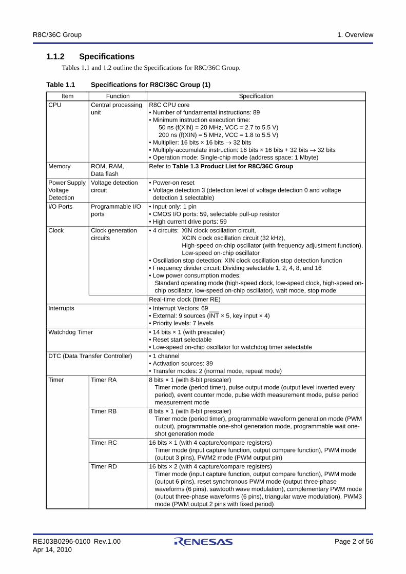
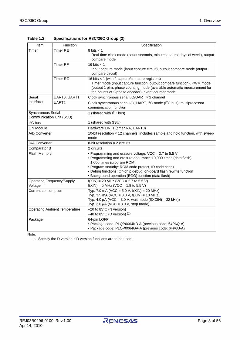
1.1.2 SpecificationsTables 1.1 and 1.2 outline the Specifications for R8C/36C Group.
Table 1.1 Specifications for R8C/36C Group (1)Item Function Specification
CPU Central processing unit
R8C CPU core• Number of fundamental instructions: 89• Minimum instruction execution time:
50 ns (f(XIN) = 20 MHz, VCC = 2.7 to 5.5 V)200 ns (f(XIN) = 5 MHz, VCC = 1.8 to 5.5 V)
• Multiplier: 16 bits × 16 bits → 32 bits• Multiply-accumulate instruction: 16 bits × 16 bits + 32 bits → 32 bits• Operation mode: Single-chip mode (address space: 1 Mbyte)
Memory ROM, RAM, Data flash
Refer to Table 1.3 Product List for R8C/36C Group
Power Supply Voltage Detection
Voltage detection circuit
• Power-on reset• Voltage detection 3 (detection level of voltage detection 0 and voltage
detection 1 selectable)I/O Ports Programmable I/O
ports• Input-only: 1 pin• CMOS I/O ports: 59, selectable pull-up resistor• High current drive ports: 59
Clock Clock generation circuits
• 4 circuits: XIN clock oscillation circuit, XCIN clock oscillation circuit (32 kHz), High-speed on-chip oscillator (with frequency adjustment function),Low-speed on-chip oscillator
• Oscillation stop detection: XIN clock oscillation stop detection function• Frequency divider circuit: Dividing selectable 1, 2, 4, 8, and 16• Low power consumption modes:
Standard operating mode (high-speed clock, low-speed clock, high-speed on-chip oscillator, low-speed on-chip oscillator), wait mode, stop mode
Real-time clock (timer RE)Interrupts • Interrupt Vectors: 69
• External: 9 sources (INT × 5, key input × 4)• Priority levels: 7 levels
Watchdog Timer • 14 bits × 1 (with prescaler)• Reset start selectable• Low-speed on-chip oscillator for watchdog timer selectable
DTC (Data Transfer Controller) • 1 channel• Activation sources: 39• Transfer modes: 2 (normal mode, repeat mode)
Timer Timer RA 8 bits × 1 (with 8-bit prescaler)Timer mode (period timer), pulse output mode (output level inverted every period), event counter mode, pulse width measurement mode, pulse period measurement mode
Timer RB 8 bits × 1 (with 8-bit prescaler)Timer mode (period timer), programmable waveform generation mode (PWM output), programmable one-shot generation mode, programmable wait one-shot generation mode
Timer RC 16 bits × 1 (with 4 capture/compare registers)Timer mode (input capture function, output compare function), PWM mode (output 3 pins), PWM2 mode (PWM output pin)
Timer RD 16 bits × 2 (with 4 capture/compare registers)Timer mode (input capture function, output compare function), PWM mode (output 6 pins), reset synchronous PWM mode (output three-phase waveforms (6 pins), sawtooth wave modulation), complementary PWM mode (output three-phase waveforms (6 pins), triangular wave modulation), PWM3 mode (PWM output 2 pins with fixed period)
R8C/36C Group 1. Overview
REJ03B0296-0100 Rev.1.00 Page 3 of 56Apr 14, 2010
Note:1. Specify the D version if D version functions are to be used.
Table 1.2 Specifications for R8C/36C Group (2)Item Function Specification
Timer Timer RE 8 bits × 1Real-time clock mode (count seconds, minutes, hours, days of week), output compare mode
Timer RF 16 bits × 1Input capture mode (input capture circuit), output compare mode (output compare circuit)
Timer RG 16 bits × 1 (with 2 capture/compare registers)Timer mode (input capture function, output compare function), PWM mode (output 1 pin), phase counting mode (available automatic measurement for the counts of 2-phase encoder), event counter mode
Serial Interface
UART0, UART1 Clock synchronous serial I/O/UART × 2 channelUART2 Clock synchronous serial I/O, UART, I2C mode (I2C bus), multiprocessor
communication functionSynchronous Serial Communication Unit (SSU)
1 (shared with I2C bus)
I2C bus 1 (shared with SSU)LIN Module Hardware LIN: 1 (timer RA, UART0)A/D Converter 10-bit resolution × 12 channels, includes sample and hold function, with sweep
modeD/A Converter 8-bit resolution × 2 circuitsComparator B 2 circuitsFlash Memory • Programming and erasure voltage: VCC = 2.7 to 5.5 V
• Programming and erasure endurance:10,000 times (data flash)1,000 times (program ROM)
• Program security: ROM code protect, ID code check• Debug functions: On-chip debug, on-board flash rewrite function• Background operation (BGO) function (data flash)
Operating Frequency/Supply Voltage
f(XIN) = 20 MHz (VCC = 2.7 to 5.5 V)f(XIN) = 5 MHz (VCC = 1.8 to 5.5 V)
Current consumption Typ. 7.0 mA (VCC = 5.0 V, f(XIN) = 20 MHz)Typ. 3.5 mA (VCC = 3.0 V, f(XIN) = 10 MHz)Typ. 4.0 µA (VCC = 3.0 V, wait mode (f(XCIN) = 32 kHz))Typ. 2.0 µA (VCC = 3.0 V, stop mode)
Operating Ambient Temperature −20 to 85°C (N version)−40 to 85°C (D version) (1)
Package 64-pin LQFP• Package code: PLQP0064KB-A (previous code: 64P6Q-A)• Package code: PLQP0064GA-A (previous code: 64P6U-A)
R8C/36C Group 1. Overview
REJ03B0296-0100 Rev.1.00 Page 4 of 56Apr 14, 2010
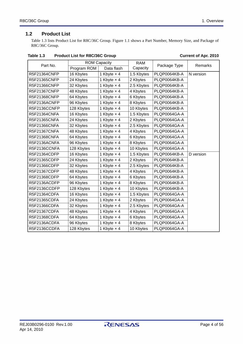
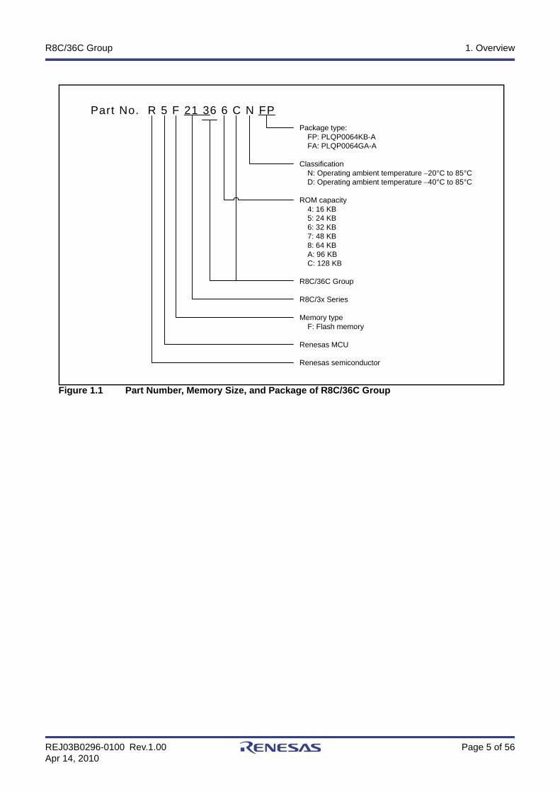
1.2 Product ListTable 1.3 lists Product List for R8C/36C Group. Figure 1.1 shows a Part Number, Memory Size, and Package ofR8C/36C Group.
Table 1.3 Product List for R8C/36C Group Current of Apr. 2010
Part No.ROM Capacity RAM
Capacity Package Type RemarksProgram ROM Data flash
R5F21364CNFP 16 Kbytes 1 Kbyte × 4 1.5 Kbytes PLQP0064KB-A N versionR5F21365CNFP 24 Kbytes 1 Kbyte × 4 2 Kbytes PLQP0064KB-AR5F21366CNFP 32 Kbytes 1 Kbyte × 4 2.5 Kbytes PLQP0064KB-AR5F21367CNFP 48 Kbytes 1 Kbyte × 4 4 Kbytes PLQP0064KB-AR5F21368CNFP 64 Kbytes 1 Kbyte × 4 6 Kbytes PLQP0064KB-AR5F2136ACNFP 96 Kbytes 1 Kbyte × 4 8 Kbytes PLQP0064KB-AR5F2136CCNFP 128 Kbytes 1 Kbyte × 4 10 Kbytes PLQP0064KB-AR5F21364CNFA 16 Kbytes 1 Kbyte × 4 1.5 Kbytes PLQP0064GA-AR5F21365CNFA 24 Kbytes 1 Kbyte × 4 2 Kbytes PLQP0064GA-AR5F21366CNFA 32 Kbytes 1 Kbyte × 4 2.5 Kbytes PLQP0064GA-AR5F21367CNFA 48 Kbytes 1 Kbyte × 4 4 Kbytes PLQP0064GA-AR5F21368CNFA 64 Kbytes 1 Kbyte × 4 6 Kbytes PLQP0064GA-AR5F2136ACNFA 96 Kbytes 1 Kbyte × 4 8 Kbytes PLQP0064GA-AR5F2136CCNFA 128 Kbytes 1 Kbyte × 4 10 Kbytes PLQP0064GA-AR5F21364CDFP 16 Kbytes 1 Kbyte × 4 1.5 Kbytes PLQP0064KB-A D versionR5F21365CDFP 24 Kbytes 1 Kbyte × 4 2 Kbytes PLQP0064KB-AR5F21366CDFP 32 Kbytes 1 Kbyte × 4 2.5 Kbytes PLQP0064KB-AR5F21367CDFP 48 Kbytes 1 Kbyte × 4 4 Kbytes PLQP0064KB-AR5F21368CDFP 64 Kbytes 1 Kbyte × 4 6 Kbytes PLQP0064KB-AR5F2136ACDFP 96 Kbytes 1 Kbyte × 4 8 Kbytes PLQP0064KB-AR5F2136CCDFP 128 Kbytes 1 Kbyte × 4 10 Kbytes PLQP0064KB-AR5F21364CDFA 16 Kbytes 1 Kbyte × 4 1.5 Kbytes PLQP0064GA-AR5F21365CDFA 24 Kbytes 1 Kbyte × 4 2 Kbytes PLQP0064GA-AR5F21366CDFA 32 Kbytes 1 Kbyte × 4 2.5 Kbytes PLQP0064GA-AR5F21367CDFA 48 Kbytes 1 Kbyte × 4 4 Kbytes PLQP0064GA-AR5F21368CDFA 64 Kbytes 1 Kbyte × 4 6 Kbytes PLQP0064GA-AR5F2136ACDFA 96 Kbytes 1 Kbyte × 4 8 Kbytes PLQP0064GA-AR5F2136CCDFA 128 Kbytes 1 Kbyte × 4 10 Kbytes PLQP0064GA-A
R8C/36C Group 1. Overview
REJ03B0296-0100 Rev.1.00 Page 5 of 56Apr 14, 2010
Figure 1.1 Part Number, Memory Size, and Package of R8C/36C Group
Part No. R 5 F 21 36 6 C N FPPackage type:
FP: PLQP0064KB-AFA: PLQP0064GA-A
ClassificationN: Operating ambient temperature −20°C to 85°CD: Operating ambient temperature −40°C to 85°C
ROM capacity4: 16 KB5: 24 KB6: 32 KB7: 48 KB8: 64 KBA: 96 KBC: 128 KB
R8C/36C Group
R8C/3x Series
Memory typeF: Flash memory
Renesas MCU
Renesas semiconductor
R8C/36C Group 1. Overview
REJ03B0296-0100 Rev.1.00 Page 6 of 56Apr 14, 2010
1.3 Block DiagramFigure 1.2 shows a Block Diagram.
Figure 1.2 Block Diagram
D/A converter(8 bits × 2)
R8C CPU core
System clock generationcircuit
XIN-XOUTHigh-speed on-chip oscillatorLow-speed on-chip oscillator
XCIN-XCOUT
Memory
ROM (1)
RAM (2)
Multiplier
R0H R0LR1H
R2R3
R1L
A0A1FB
SBUSPISP
INTBPC
FLG
I/O ports
Notes:1. ROM size varies with MCU type.2. RAM size varies with MCU type.
Timers
Timer RA (8 bits × 1)Timer RB (8 bits × 1)
Timer RC (16 bits × 1)Timer RD (16 bits × 2)Timer RE (8 bits × 1)Timer RF (16 bits × 1)Timer RG (16 bits × 1)
UART orclock synchronous serial I/O
(8 bits × 3)
I2C bus or SSU(8 bits × 1)
Peripheral functions
Watchdog timer(14 bits)
A/D converter(10 bits × 12 channels)
LIN module
Comparator B
Voltage detection circuit
DTC
Low-speed on-chip oscillatorfor watchdog timer
7
Port P5
5 1
Port P4
8
Port P3
8
Port P0
8
Port P1
8
Port P2
8
Port P6
7
Port P8
R8C/36C Group 1. Overview
REJ03B0296-0100 Rev.1.00 Page 7 of 56Apr 14, 2010
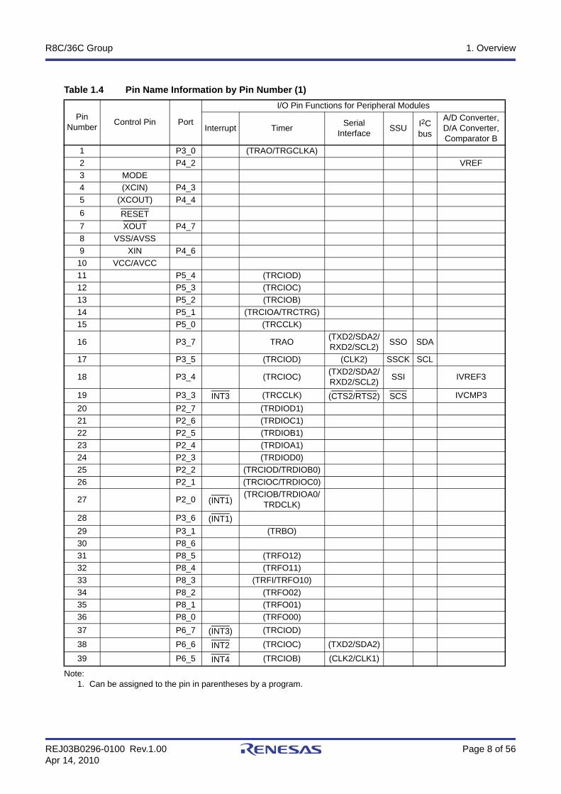
1.4 Pin AssignmentFigure 1.3 shows Pin Assignment (Top View). Tables 1.4 and 1.5 outline the Pin Name Information by Pin Number.
Figure 1.3 Pin Assignment (Top View)
43 42 41 40 39 38 37 36
24
17
18
19
20
21
22
23
1 3 4 5 6 7 8 9 10 11 122
35 34 33
13 14 15 16
25
26
27
28
29
30
31
32
4445464748
R8C/36C Group
PLQP0064KB-A (64P6Q-A)PLQP0064GA-A (64P6U-A)
(Top view)
P0_7/AN0/DA1(/TRCIOC)P0_6/AN1/DA0(/TRCIOD)
P0_5/AN2(/TRCIOB)P0_4/AN3/TREO(/TRCIOB)P0_3/AN4(/CLK1/TRCIOB)
P0_2/AN5(/RXD1/TRCIOA/TRCTRG)P0_1/AN6(/TXD1/TRCIOA/TRCTRG)
P0_0/AN7(/TRCIOA/TRCTRG)P6_4(/RXD1)P6_3(/TXD1)P6_2(/CLK1)
P6_1P6_0(/TREO)
P5_7(/TRGIOB)P5_6(/TRAO/TRGIOA)
P3_2(/INT1/INT2/TRAIO/TRGCLKB)
P8_4(/TRFO11)P8_5(/TRFO12)P8_6P3_1(/TRBO)P3_6(/INT1)P2_0(/INT1/TRCIOB/TRDIOA0/TRDCLK)P2_1(/TRCIOC/TRDIOC0)P2_2(/TRCIOD/TRDIOB0)P2_3(/TRDIOD0)P2_4(/TRDIOA1)P2_5(/TRDIOB1)P2_6(/TRDIOC1)P2_7(/TRDIOD1)P3_3/IVCMP3/INT3/SCS(/CTS2/RTS2/TRCCLK)P3_4/IVREF3/SSI(/RXD2/SCL2/TXD2/SDA2/TRCIOC)P3_5/SCL/SSCK(/CLK2/TRCIOD)
P3_0
(/TR
AO/T
RG
CLK
A)
P4_2
/VR
EFM
OD
EP
4_3(
/XC
IN)
P4_4
(/XC
OU
T)R
ESET
P4_
7/X
OU
TV
SS/
AVS
SP
4_6/
XIN
VC
C/A
VCC
P5_4
(/TR
CIO
D)
P5_3
(/TR
CIO
C)
P5_
2(/T
RC
IOB
)P5
_1(/T
RC
IOA
/TR
CTR
G)
P5_0
(/TR
CC
LK)
P3_
7/S
DA
/SS
O/T
RAO
(/RX
D2/
SCL2
/TX
D2/
SD
A2)
P1_0
/AN
8/KI
0(/T
RC
IOD
)P1
_1/A
N9/
KI1(
/TR
CIO
A/TR
CTR
G)
P1_2
/AN
10/K
I2(/T
RC
IOB
)P1
_3/A
N11
/KI3
/TR
BO(/T
RC
IOC
)P1
_4(/T
XD0/
TRC
CLK
)P1
_5(/I
NT1
/RX
D0/
TRAI
O)
P1_6
/IVR
EF1
(/CLK
0)P1
_7/IV
CM
P1/
INT1
(/TR
AIO
)P4
_5/A
DTR
G/IN
T0(/R
XD
2/SC
L2)
P6_5
/INT4
(/CLK
1/C
LK2/
TRC
IOB
)P6
_6/IN
T2(/T
XD
2/SD
A2/
TRC
IOC
)P6
_7(/I
NT3
/TR
CIO
D)
P8_0
(/TR
FO00
)P8
_1(/T
RFO
01)
P8_2
(/TR
FO02
)P8
_3(/T
RFI
/TR
FO10
)
Notes:1. Can be assigned to the pin in parentheses by a program.2. P4_2 is an input-only pin.3. Confirm the pin 1 position on the package by referring to the package dimensions.
60
59
58
57
56
55
54
53
52
51
50
49
61
62
63
64
R8C/36C Group 1. Overview
REJ03B0296-0100 Rev.1.00 Page 8 of 56Apr 14, 2010
Note:1. Can be assigned to the pin in parentheses by a program.
Table 1.4 Pin Name Information by Pin Number (1)
Pin Number Control Pin Port
I/O Pin Functions for Peripheral Modules
Interrupt Timer Serial Interface SSU I2C
bus
A/D Converter, D/A Converter, Comparator B
1 P3_0 (TRAO/TRGCLKA)2 P4_2 VREF3 MODE4 (XCIN) P4_35 (XCOUT) P4_46 RESET7 XOUT P4_78 VSS/AVSS9 XIN P4_6
10 VCC/AVCC11 P5_4 (TRCIOD)12 P5_3 (TRCIOC)13 P5_2 (TRCIOB)14 P5_1 (TRCIOA/TRCTRG)15 P5_0 (TRCCLK)
16 P3_7 TRAO (TXD2/SDA2/RXD2/SCL2) SSO SDA
17 P3_5 (TRCIOD) (CLK2) SSCK SCL
18 P3_4 (TRCIOC) (TXD2/SDA2/RXD2/SCL2) SSI IVREF3
19 P3_3 INT3 (TRCCLK) (CTS2/RTS2) SCS IVCMP320 P2_7 (TRDIOD1)21 P2_6 (TRDIOC1)22 P2_5 (TRDIOB1)23 P2_4 (TRDIOA1)24 P2_3 (TRDIOD0)25 P2_2 (TRCIOD/TRDIOB0)26 P2_1 (TRCIOC/TRDIOC0)
27 P2_0 (INT1)(TRCIOB/TRDIOA0/
TRDCLK)28 P3_6 (INT1)29 P3_1 (TRBO)30 P8_631 P8_5 (TRFO12)32 P8_4 (TRFO11)33 P8_3 (TRFI/TRFO10)34 P8_2 (TRFO02)35 P8_1 (TRFO01)36 P8_0 (TRFO00)37 P6_7 (INT3) (TRCIOD)
38 P6_6 INT2 (TRCIOC) (TXD2/SDA2)
39 P6_5 INT4 (TRCIOB) (CLK2/CLK1)
R8C/36C Group 1. Overview
REJ03B0296-0100 Rev.1.00 Page 9 of 56Apr 14, 2010
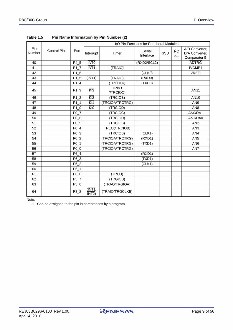
Note:1. Can be assigned to the pin in parentheses by a program.
Table 1.5 Pin Name Information by Pin Number (2)
Pin Number Control Pin Port
I/O Pin Functions for Peripheral Modules
Interrupt Timer Serial Interface SSU I2C
bus
A/D Converter, D/A Converter, Comparator B
40 P4_5 INT0 (RXD2/SCL2) ADTRG41 P1_7 INT1 (TRAIO) IVCMP142 P1_6 (CLK0) IVREF143 P1_5 (INT1) (TRAIO) (RXD0)44 P1_4 (TRCCLK) (TXD0)
45 P1_3 KI3 TRBO(/TRCIOC) AN11
46 P1_2 KI2 (TRCIOB) AN1047 P1_1 KI1 (TRCIOA/TRCTRG) AN948 P1_0 KI0 (TRCIOD) AN849 P0_7 (TRCIOC) AN0/DA150 P0_6 (TRCIOD) AN1/DA051 P0_5 (TRCIOB) AN252 P0_4 TREO(/TRCIOB) AN353 P0_3 (TRCIOB) (CLK1) AN454 P0_2 (TRCIOA/TRCTRG) (RXD1) AN555 P0_1 (TRCIOA/TRCTRG) (TXD1) AN656 P0_0 (TRCIOA/TRCTRG) AN757 P6_4 (RXD1)58 P6_3 (TXD1)59 P6_2 (CLK1)60 P6_161 P6_0 (TREO)62 P5_7 (TRGIOB)63 P5_6 (TRAO/TRGIOA)
64 P3_2 (INT1/INT2) (TRAIO/TRGCLKB)
R8C/36C Group 1. Overview
REJ03B0296-0100 Rev.1.00 Page 10 of 56Apr 14, 2010
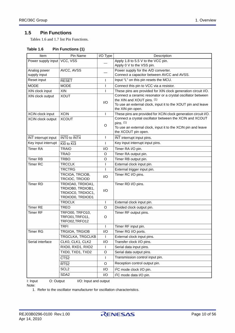
1.5 Pin FunctionsTables 1.6 and 1.7 list Pin Functions.
I: Input O: Output I/O: Input and outputNote:
1. Refer to the oscillator manufacturer for oscillation characteristics.
Table 1.6 Pin Functions (1)Item Pin Name I/O Type Description
Power supply input VCC, VSS — Apply 1.8 to 5.5 V to the VCC pin.Apply 0 V to the VSS pin.
Analog power supply input
AVCC, AVSS — Power supply for the A/D converter.Connect a capacitor between AVCC and AVSS.
Reset input RESET I Input “L” on this pin resets the MCU.
MODE MODE I Connect this pin to VCC via a resistor.XIN clock input XIN I These pins are provided for XIN clock generation circuit I/O.
Connect a ceramic resonator or a crystal oscillator between the XIN and XOUT pins. (1)
To use an external clock, input it to the XOUT pin and leave the XIN pin open.
XIN clock output XOUT
I/O
XCIN clock input XCIN I These pins are provided for XCIN clock generation circuit I/O. Connect a crystal oscillator between the XCIN and XCOUT pins. (1)
To use an external clock, input it to the XCIN pin and leave the XCOUT pin open.
XCIN clock output XCOUT
O
INT interrupt input INT0 to INT4 I INT interrupt input pins.Key input interrupt KI0 to KI3 I Key input interrupt input pins.
Timer RA TRAIO I/O Timer RA I/O pin.TRAO O Timer RA output pin.
Timer RB TRBO O Timer RB output pin.Timer RC TRCCLK I External clock input pin.
TRCTRG I External trigger input pin.TRCIOA, TRCIOB,TRCIOC, TRCIOD I/O Timer RC I/O pins.
Timer RD TRDIOA0, TRDIOA1, TRDIOB0, TRDIOB1, TRDIOC0, TRDIOC1, TRDIOD0, TRDIOD1
I/O
Timer RD I/O pins.
TRDCLK I External clock input pin.Timer RE TREO O Divided clock output pin.Timer RF TRFO00, TRFO10,
TRFO01,TRFO11,TRFO02,TRFO12
OTimer RF output pins.
TRFI I Timer RF input pin.Timer RG TRGIOA, TRGIOB I/O Timer RG I/O ports.
TRGCLKA, TRGCLKB I External clock input pins.Serial interface CLK0, CLK1, CLK2 I/O Transfer clock I/O pins.
RXD0, RXD1, RXD2 I Serial data input pins.TXD0, TXD1, TXD2 O Serial data output pins.
CTS2 I Transmission control input pin.
RTS2 O Reception control output pin.
SCL2 I/O I2C mode clock I/O pin.SDA2 I/O I2C mode data I/O pin.
R8C/36C Group 1. Overview
REJ03B0296-0100 Rev.1.00 Page 11 of 56Apr 14, 2010
I: Input O: Output I/O: Input and output
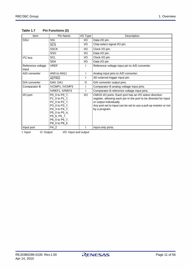
Table 1.7 Pin Functions (2)Item Pin Name I/O Type Description
SSU SSI I/O Data I/O pin.
SCS I/O Chip-select signal I/O pin.
SSCK I/O Clock I/O pin.SSO I/O Data I/O pin.
I2C bus SCL I/O Clock I/O pinSDA I/O Data I/O pin
Reference voltage input
VREF I Reference voltage input pin to A/D converter.
A/D converter AN0 to AN11 I Analog input pins to A/D converter.
ADTRG I AD external trigger input pin.
D/A converter DA0, DA1 O D/A converter output pins.Comparator B IVCMP1, IVCMP3 I Comparator B analog voltage input pins.
IVREF1, IVREF3 I Comparator B reference voltage input pins.I/O port P0_0 to P0_7,
P1_0 to P1_7, P2_0 to P2_7, P3_0 to P3_7, P4_3 to P4_7, P5_0 to P5_4, P5_6, P5_7, P6_0 to P6_7, P8_0 to P8_6
I/O CMOS I/O ports. Each port has an I/O select direction register, allowing each pin in the port to be directed for input or output individually.Any port set to input can be set to use a pull-up resistor or not by a program.
Input port P4_2 I Input-only ports.
R8C/36C Group 2. Central Processing Unit (CPU)
REJ03B0296-0100 Rev.1.00 Page 12 of 56Apr 14, 2010
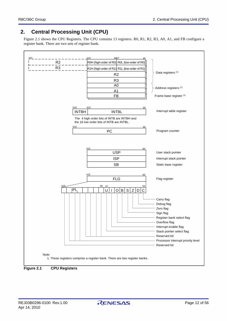
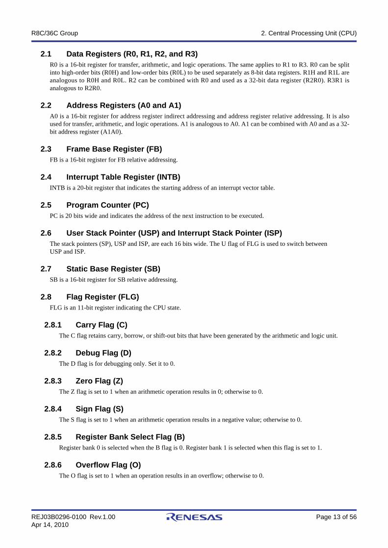
2. Central Processing Unit (CPU)Figure 2.1 shows the CPU Registers. The CPU contains 13 registers. R0, R1, R2, R3, A0, A1, and FB configure aregister bank. There are two sets of register bank.
Figure 2.1 CPU Registers
R2b31 b15 b8b7 b0
Data registers (1)
Address registers (1)
R3R0H (high-order of R0)
R2R3A0A1
INTBHb15b19 b0
INTBL
FB Frame base register (1)
The 4 high order bits of INTB are INTBH andthe 16 low order bits of INTB are INTBL.
Interrupt table register
b19 b0
USP
Program counter
ISPSB
User stack pointer
Interrupt stack pointer
Static base register
PC
FLG Flag register
Carry flagDebug flagZero flagSign flagRegister bank select flagOverflow flagInterrupt enable flagStack pointer select flagReserved bitProcessor interrupt priority levelReserved bit
CIPL DZSBOIU
b15 b0
b15 b0
b15 b0b8 b7
Note:1. These registers comprise a register bank. There are two register banks.
R1H (high-order of R1)
R0L (low-order of R0)
R1L (low-order of R1)
R8C/36C Group 2. Central Processing Unit (CPU)
REJ03B0296-0100 Rev.1.00 Page 13 of 56Apr 14, 2010
2.1 Data Registers (R0, R1, R2, and R3)R0 is a 16-bit register for transfer, arithmetic, and logic operations. The same applies to R1 to R3. R0 can be splitinto high-order bits (R0H) and low-order bits (R0L) to be used separately as 8-bit data registers. R1H and R1L areanalogous to R0H and R0L. R2 can be combined with R0 and used as a 32-bit data register (R2R0). R3R1 isanalogous to R2R0.
2.2 Address Registers (A0 and A1)A0 is a 16-bit register for address register indirect addressing and address register relative addressing. It is alsoused for transfer, arithmetic, and logic operations. A1 is analogous to A0. A1 can be combined with A0 and as a 32-bit address register (A1A0).
2.3 Frame Base Register (FB)FB is a 16-bit register for FB relative addressing.
2.4 Interrupt Table Register (INTB)INTB is a 20-bit register that indicates the starting address of an interrupt vector table.
2.5 Program Counter (PC)PC is 20 bits wide and indicates the address of the next instruction to be executed.
2.6 User Stack Pointer (USP) and Interrupt Stack Pointer (ISP)The stack pointers (SP), USP and ISP, are each 16 bits wide. The U flag of FLG is used to switch betweenUSP and ISP.
2.7 Static Base Register (SB)SB is a 16-bit register for SB relative addressing.
2.8 Flag Register (FLG)FLG is an 11-bit register indicating the CPU state.
2.8.1 Carry Flag (C)The C flag retains carry, borrow, or shift-out bits that have been generated by the arithmetic and logic unit.
2.8.2 Debug Flag (D)The D flag is for debugging only. Set it to 0.
2.8.3 Zero Flag (Z)The Z flag is set to 1 when an arithmetic operation results in 0; otherwise to 0.
2.8.4 Sign Flag (S)The S flag is set to 1 when an arithmetic operation results in a negative value; otherwise to 0.
2.8.5 Register Bank Select Flag (B)Register bank 0 is selected when the B flag is 0. Register bank 1 is selected when this flag is set to 1.
2.8.6 Overflow Flag (O)The O flag is set to 1 when an operation results in an overflow; otherwise to 0.
R8C/36C Group 2. Central Processing Unit (CPU)
REJ03B0296-0100 Rev.1.00 Page 14 of 56Apr 14, 2010
2.8.7 Interrupt Enable Flag (I)The I flag enables maskable interrupts.Interrupts are disabled when the I flag is set to 0, and are enabled when the I flag is set to 1. The I flag is set to 0when an interrupt request is acknowledged.
2.8.8 Stack Pointer Select Flag (U)ISP is selected when the U flag is set to 0; USP is selected when the U flag is set to 1.The U flag is set to 0 when a hardware interrupt request is acknowledged or the INT instruction of softwareinterrupt numbers 0 to 31 is executed.
2.8.9 Processor Interrupt Priority Level (IPL)IPL is 3 bits wide and assigns processor interrupt priority levels from level 0 to level 7.If a requested interrupt has higher priority than IPL, the interrupt is enabled.
2.8.10 Reserved BitIf necessary, set to 0. When read, the content is undefined.
R8C/36C Group 3. Memory
REJ03B0296-0100 Rev.1.00 Page 15 of 56Apr 14, 2010
3. Memory
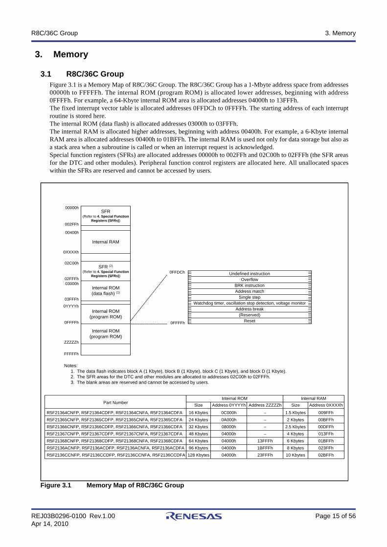
3.1 R8C/36C GroupFigure 3.1 is a Memory Map of R8C/36C Group. The R8C/36C Group has a 1-Mbyte address space from addresses00000h to FFFFFh. The internal ROM (program ROM) is allocated lower addresses, beginning with address0FFFFh. For example, a 64-Kbyte internal ROM area is allocated addresses 04000h to 13FFFh.The fixed interrupt vector table is allocated addresses 0FFDCh to 0FFFFh. The starting address of each interruptroutine is stored here. The internal ROM (data flash) is allocated addresses 03000h to 03FFFh. The internal RAM is allocated higher addresses, beginning with address 00400h. For example, a 6-Kbyte internalRAM area is allocated addresses 00400h to 01BFFh. The internal RAM is used not only for data storage but also asa stack area when a subroutine is called or when an interrupt request is acknowledged.Special function registers (SFRs) are allocated addresses 00000h to 002FFh and 02C00h to 02FFFh (the SFR areasfor the DTC and other modules). Peripheral function control registers are allocated here. All unallocated spaceswithin the SFRs are reserved and cannot be accessed by users.
Figure 3.1 Memory Map of R8C/36C Group
0FFFFh
0FFDCh
Notes:1. The data flash indicates block A (1 Kbyte), block B (1 Kbyte), block C (1 Kbyte), and block D (1 Kbyte).2. The SFR areas for the DTC and other modules are allocated to addresses 02C00h to 02FFFh.3. The blank areas are reserved and cannot be accessed by users.
Internal RAMSize Address 0XXXXh
1.5 Kbytes2 Kbytes
2.5 Kbytes4 Kbytes6 Kbytes8 Kbytes10 Kbytes
009FFh00BFFh00DFFh013FFh01BFFh023FFh02BFFh
Part NumberInternal ROM
Size Address 0YYYYh
R5F21364CNFP, R5F21364CDFP, R5F21364CNFA, R5F21364CDFAR5F21365CNFP, R5F21365CDFP, R5F21365CNFA, R5F21365CDFAR5F21366CNFP, R5F21366CDFP, R5F21366CNFA, R5F21366CDFAR5F21367CNFP, R5F21367CDFP, R5F21367CNFA, R5F21367CDFAR5F21368CNFP, R5F21368CDFP, R5F21368CNFA, R5F21368CDFAR5F2136ACNFP, R5F2136ACDFP, R5F2136ACNFA, R5F2136ACDFAR5F2136CCNFP, R5F2136CCDFP, R5F2136CCNFA, R5F2136CCDFA
16 Kbytes24 Kbytes32 Kbytes48 Kbytes64 Kbytes96 Kbytes
128 Kbytes
0C000h0A000h08000h04000h04000h04000h04000h
Address ZZZZZh
––––
13FFFh1BFFFh23FFFh
FFFFFh
0FFFFh
0YYYYh
0XXXXh
00400h
002FFh
00000h
Internal ROM(program ROM)
Internal RAM
SFR(Refer to 4. Special Function
Registers (SFRs))
02FFFh
02C00hSFR (2)
(Refer to 4. Special FunctionRegisters (SFRs))
ZZZZZh
03FFFh
03000hInternal ROM(data flash) (1)
Internal ROM(program ROM)
Undefined instructionOverflow
BRK instructionAddress match
Single stepWatchdog timer, oscillation stop detection, voltage monitor
Address break(Reserved)
Reset
R8C/36C Group 4. Special Function Registers (SFRs)
REJ03B0296-0100 Rev.1.00 Page 16 of 56Apr 14, 2010
4. Special Function Registers (SFRs)An SFR (special function register) is a control register for a peripheral function. Tables 4.1 to 4.12 list the specialfunction registers. Table 4.13 lists the ID Code Areas and Option Function Select Area.
Table 4.1 SFR Information (1) (1)
X: UndefinedNotes:
1. The blank areas are reserved and cannot be accessed by users.2. The CWR bit in the RSTFR register is set to 0 after power-on and voltage monitor 0 reset. Hardware reset, software reset, or watchdog timer
reset does not affect this bit. 3. The CSPROINI bit in the OFS register is set to 0.4. The LVDAS bit in the OFS register is set to 1.5. The LVDAS bit in the OFS register is set to 0.
Address Register Symbol After Reset0000h0001h0002h0003h0004h Processor Mode Register 0 PM0 00h0005h Processor Mode Register 1 PM1 00h0006h System Clock Control Register 0 CM0 00101000b0007h System Clock Control Register 1 CM1 00100000b0008h Module Standby Control Register MSTCR 00h0009h System Clock Control Register 3 CM3 00h000Ah Protect Register PRCR 00h000Bh Reset Source Determination Register RSTFR 0XXXXXXXb (2)
000Ch Oscillation Stop Detection Register OCD 00000100b000Dh Watchdog Timer Reset Register WDTR XXh000Eh Watchdog Timer Start Register WDTS XXh000Fh Watchdog Timer Control Register WDTC 00111111b0010h0011h0012h0013h0014h0015h High-Speed On-Chip Oscillator Control Register 7 FRA7 When shipping0016h0017h0018h0019h001Ah001Bh001Ch Count Source Protection Mode Register CSPR 00h
10000000b (3)
001Dh001Eh001Fh0020h0021h0022h0023h High-Speed On-Chip Oscillator Control Register 0 FRA0 00h0024h High-Speed On-Chip Oscillator Control Register 1 FRA1 When shipping0025h High-Speed On-Chip Oscillator Control Register 2 FRA2 00h0026h On-Chip Reference Voltage Control Register OCVREFCR 00h0027h0028h Clock Prescaler Reset Flag CPSRF 00h0029h High-Speed On-Chip Oscillator Control Register 4 FRA4 When shipping002Ah High-Speed On-Chip Oscillator Control Register 5 FRA5 When shipping002Bh High-Speed On-Chip Oscillator Control Register 6 FRA6 When shipping002Ch002Dh002Eh002Fh High-Speed On-Chip Oscillator Control Register 3 FRA3 When shipping0030h Voltage Monitor Circuit Control Register CMPA 00h0031h Voltage Monitor Circuit Edge Select Register VCAC 00h0032h0033h Voltage Detect Register 1 VCA1 00001000b0034h Voltage Detect Register 2 VCA2 00h (4)
00100000b (5)
0035h0036h Voltage Detection 1 Level Select Register VD1LS 00000111b0037h0038h Voltage Monitor 0 Circuit Control Register VW0C 1100X010b (4)
1100X011b (5)
0039h Voltage Monitor 1 Circuit Control Register VW1C 10001010b
R8C/36C Group 4. Special Function Registers (SFRs)
REJ03B0296-0100 Rev.1.00 Page 17 of 56Apr 14, 2010
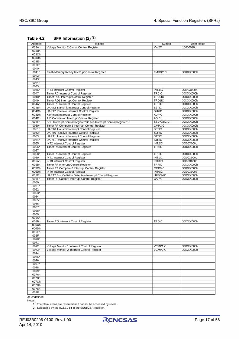
Table 4.2 SFR Information (2) (1)
X: UndefinedNotes:
1. The blank areas are reserved and cannot be accessed by users.2. Selectable by the IICSEL bit in the SSUIICSR register.
Address Register Symbol After Reset003Ah Voltage Monitor 2 Circuit Control Register VW2C 10000010b003Bh003Ch003Dh003Eh003Fh0040h0041h Flash Memory Ready Interrupt Control Register FMRDYIC XXXXX000b0042h0043h0044h0045h0046h INT4 Interrupt Control Register INT4IC XX00X000b0047h Timer RC Interrupt Control Register TRCIC XXXXX000b0048h Timer RD0 Interrupt Control Register TRD0IC XXXXX000b0049h Timer RD1 Interrupt Control Register TRD1IC XXXXX000b004Ah Timer RE Interrupt Control Register TREIC XXXXX000b004Bh UART2 Transmit Interrupt Control Register S2TIC XXXXX000b004Ch UART2 Receive Interrupt Control Register S2RIC XXXXX000b004Dh Key Input Interrupt Control Register KUPIC XXXXX000b004Eh A/D Conversion Interrupt Control Register ADIC XXXXX000b004Fh SSU Interrupt Control Register/IIC bus Interrupt Control Register (2) SSUIC/IICIC XXXXX000b0050h Timer RF Compare 1 Interrupt Control Register CMP1IC XXXXX000b0051h UART0 Transmit Interrupt Control Register S0TIC XXXXX000b0052h UART0 Receive Interrupt Control Register S0RIC XXXXX000b0053h UART1 Transmit Interrupt Control Register S1TIC XXXXX000b0054h UART1 Receive Interrupt Control Register S1RIC XXXXX000b0055h INT2 Interrupt Control Register INT2IC XX00X000b0056h Timer RA Interrupt Control Register TRAIC XXXXX000b0057h0058h Timer RB Interrupt Control Register TRBIC XXXXX000b0059h INT1 Interrupt Control Register INT1IC XX00X000b005Ah INT3 Interrupt Control Register INT3IC XX00X000b005Bh Timer RF Interrupt Control Register TRFIC XXXXX000b005Ch Timer RF Compare 0 Interrupt Control Register CMP0IC XXXXX000b005Dh INT0 Interrupt Control Register INT0IC XX00X000b005Eh UART2 Bus Collision Detection Interrupt Control Register U2BCNIC XXXXX000b005Fh Timer RF Capture Interrupt Control Register CAPIC XXXXX000b0060h0061h0062h0063h0064h0065h0066h0067h0068h0069h006Ah006Bh Timer RG Interrupt Control Register TRGIC XXXXX000b006Ch006Dh006Eh006Fh0070h0071h0072h Voltage Monitor 1 Interrupt Control Register VCMP1IC XXXXX000b0073h Voltage Monitor 2 Interrupt Control Register VCMP2IC XXXXX000b0074h0075h0076h0077h0078h0079h007Ah007Bh007Ch007Dh007Eh007Fh
R8C/36C Group 4. Special Function Registers (SFRs)
REJ03B0296-0100 Rev.1.00 Page 18 of 56Apr 14, 2010
Table 4.3 SFR Information (3) (1)
X: UndefinedNote:
1. The blank areas are reserved and cannot be accessed by users.
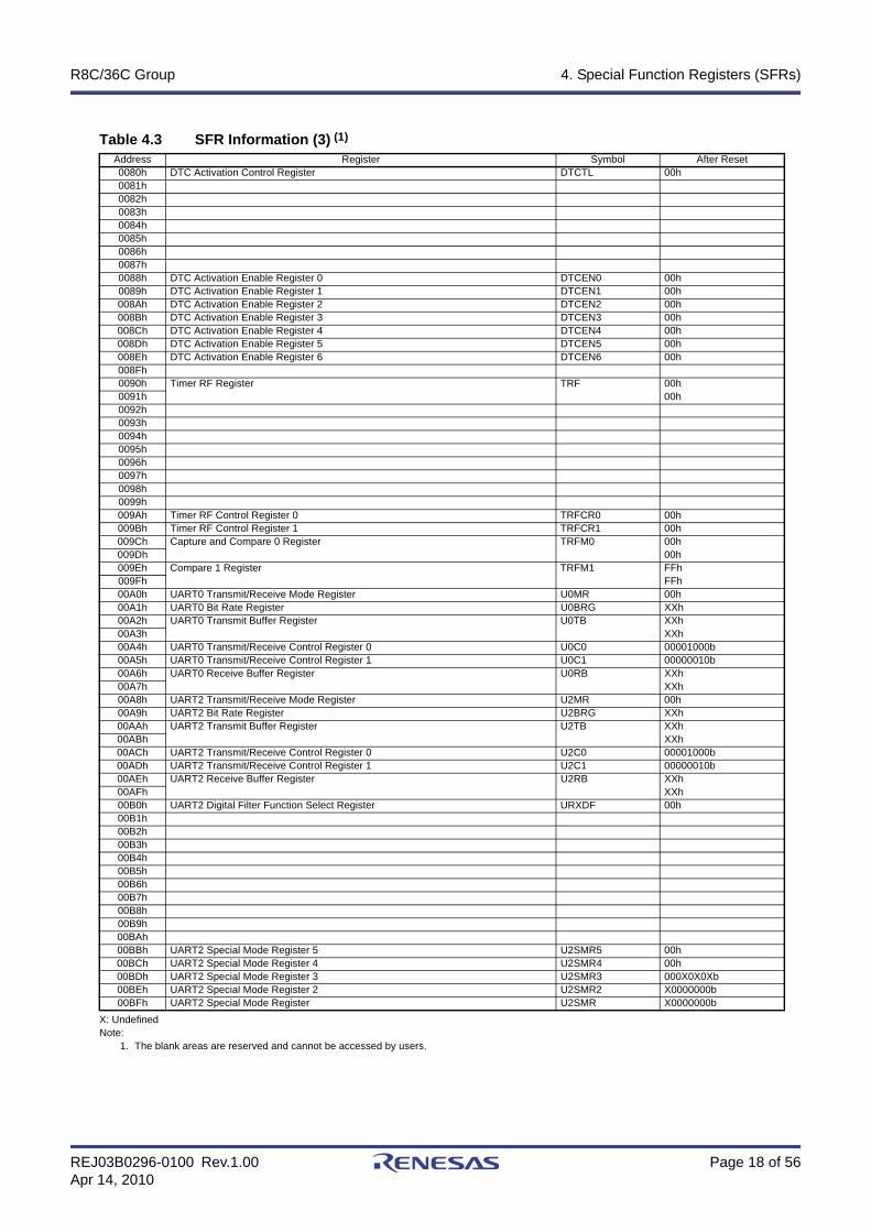
Address Register Symbol After Reset0080h DTC Activation Control Register DTCTL 00h0081h0082h0083h0084h0085h0086h0087h0088h DTC Activation Enable Register 0 DTCEN0 00h0089h DTC Activation Enable Register 1 DTCEN1 00h008Ah DTC Activation Enable Register 2 DTCEN2 00h008Bh DTC Activation Enable Register 3 DTCEN3 00h008Ch DTC Activation Enable Register 4 DTCEN4 00h008Dh DTC Activation Enable Register 5 DTCEN5 00h008Eh DTC Activation Enable Register 6 DTCEN6 00h008Fh0090h Timer RF Register TRF 00h
00h0091h0092h0093h0094h0095h0096h0097h0098h0099h009Ah Timer RF Control Register 0 TRFCR0 00h009Bh Timer RF Control Register 1 TRFCR1 00h009Ch Capture and Compare 0 Register TRFM0 00h
00h009Dh009Eh Compare 1 Register TRFM1 FFh
FFh009Fh00A0h UART0 Transmit/Receive Mode Register U0MR 00h00A1h UART0 Bit Rate Register U0BRG XXh00A2h UART0 Transmit Buffer Register U0TB XXh
XXh00A3h00A4h UART0 Transmit/Receive Control Register 0 U0C0 00001000b00A5h UART0 Transmit/Receive Control Register 1 U0C1 00000010b00A6h UART0 Receive Buffer Register U0RB XXh
XXh00A7h00A8h UART2 Transmit/Receive Mode Register U2MR 00h00A9h UART2 Bit Rate Register U2BRG XXh00AAh UART2 Transmit Buffer Register U2TB XXh
XXh00ABh00ACh UART2 Transmit/Receive Control Register 0 U2C0 00001000b00ADh UART2 Transmit/Receive Control Register 1 U2C1 00000010b00AEh UART2 Receive Buffer Register U2RB XXh
XXh00AFh00B0h UART2 Digital Filter Function Select Register URXDF 00h00B1h00B2h00B3h00B4h00B5h00B6h00B7h00B8h00B9h00BAh00BBh UART2 Special Mode Register 5 U2SMR5 00h00BCh UART2 Special Mode Register 4 U2SMR4 00h00BDh UART2 Special Mode Register 3 U2SMR3 000X0X0Xb00BEh UART2 Special Mode Register 2 U2SMR2 X0000000b00BFh UART2 Special Mode Register U2SMR X0000000b
R8C/36C Group 4. Special Function Registers (SFRs)
REJ03B0296-0100 Rev.1.00 Page 19 of 56Apr 14, 2010
Table 4.4 SFR Information (4) (1)
X: UndefinedNote:
1. The blank areas are reserved and cannot be accessed by users.
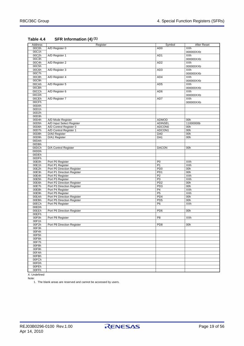
Address Register Symbol After Reset00C0h A/D Register 0 AD0 XXh
000000XXb00C1h00C2h A/D Register 1 AD1 XXh
000000XXb00C3h00C4h A/D Register 2 AD2 XXh
000000XXb00C5h00C6h A/D Register 3 AD3 XXh
000000XXb00C7h00C8h A/D Register 4 AD4 XXh
000000XXb00C9h00CAh A/D Register 5 AD5 XXh
000000XXb00CBh00CCh A/D Register 6 AD6 XXh
000000XXb00CDh00CEh A/D Register 7 AD7 XXh
000000XXb00CFh00D0h00D1h00D2h00D3h00D4h A/D Mode Register ADMOD 00h00D5h A/D Input Select Register ADINSEL 11000000b00D6h A/D Control Register 0 ADCON0 00h00D7h A/D Control Register 1 ADCON1 00h00D8h D/A0 Register DA0 00h00D9h D/A1 Register DA1 00h00DAh00DBh00DCh D/A Control Register DACON 00h00DDh00DEh00DFh00E0h Port P0 Register P0 XXh00E1h Port P1 Register P1 XXh00E2h Port P0 Direction Register PD0 00h00E3h Port P1 Direction Register PD1 00h00E4h Port P2 Register P2 XXh00E5h Port P3 Register P3 XXh00E6h Port P2 Direction Register PD2 00h00E7h Port P3 Direction Register PD3 00h00E8h Port P4 Register P4 XXh00E9h Port P5 Register P5 XXh00EAh Port P4 Direction Register PD4 00h00EBh Port P5 Direction Register PD5 00h00ECh Port P6 Register P6 XXh00EDh00EEh Port P6 Direction Register PD6 00h00EFh00F0h Port P8 Register P8 XXh00F1h00F2h Port P8 Direction Register PD8 00h00F3h00F4h00F5h00F6h00F7h00F8h00F9h00FAh00FBh00FCh00FDh00FEh00FFh
R8C/36C Group 4. Special Function Registers (SFRs)
REJ03B0296-0100 Rev.1.00 Page 20 of 56Apr 14, 2010
Table 4.5 SFR Information (5) (1)
Note:1. The blank areas are reserved and cannot be accessed by users.
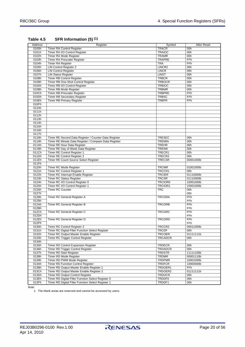
Address Register Symbol After Reset0100h Timer RA Control Register TRACR 00h0101h Timer RA I/O Control Register TRAIOC 00h0102h Timer RA Mode Register TRAMR 00h0103h Timer RA Prescaler Register TRAPRE FFh0104h Timer RA Register TRA FFh0105h LIN Control Register 2 LINCR2 00h0106h LIN Control Register LINCR 00h0107h LIN Status Register LINST 00h0108h Timer RB Control Register TRBCR 00h0109h Timer RB One-Shot Control Register TRBOCR 00h010Ah Timer RB I/O Control Register TRBIOC 00h010Bh Timer RB Mode Register TRBMR 00h010Ch Timer RB Prescaler Register TRBPRE FFh010Dh Timer RB Secondary Register TRBSC FFh010Eh Timer RB Primary Register TRBPR FFh010Fh0110h0111h0112h0113h0114h0115h0116h0117h0118h Timer RE Second Data Register / Counter Data Register TRESEC 00h0119h Timer RE Minute Data Register / Compare Data Register TREMIN 00h011Ah Timer RE Hour Data Register TREHR 00h011Bh Timer RE Day of Week Data Register TREWK 00h011Ch Timer RE Control Register 1 TRECR1 00h011Dh Timer RE Control Register 2 TRECR2 00h011Eh Timer RE Count Source Select Register TRECSR 00001000b011Fh0120h Timer RC Mode Register TRCMR 01001000b0121h Timer RC Control Register 1 TRCCR1 00h0122h Timer RC Interrupt Enable Register TRCIER 01110000b0123h Timer RC Status Register TRCSR 01110000b0124h Timer RC I/O Control Register 0 TRCIOR0 10001000b0125h Timer RC I/O Control Register 1 TRCIOR1 10001000b0126h Timer RC Counter TRC 00h
00h0127h0128h Timer RC General Register A TRCGRA FFh
FFh0129h012Ah Timer RC General Register B TRCGRB FFh
FFh012Bh012Ch Timer RC General Register C TRCGRC FFh
FFh012Dh012Eh Timer RC General Register D TRCGRD FFh
FFh012Fh0130h Timer RC Control Register 2 TRCCR2 00011000b0131h Timer RC Digital Filter Function Select Register TRCDF 00h0132h Timer RC Output Master Enable Register TRCOER 01111111b0133h Timer RC Trigger Control Register TRCADCR 00h0134h0135h Timer RD Control Expansion Register TRDECR 00h0136h Timer RD Trigger Control Register TRDADCR 00h0137h Timer RD Start Register TRDSTR 11111100b0138h Timer RD Mode Register TRDMR 00001110b0139h Timer RD PWM Mode Register TRDPMR 10001000b013Ah Timer RD Function Control Register TRDFCR 10000000b013Bh Timer RD Output Master Enable Register 1 TRDOER1 FFh013Ch Timer RD Output Master Enable Register 2 TRDOER2 01111111b013Dh Timer RD Output Control Register TRDOCR 00h013Eh Timer RD Digital Filter Function Select Register 0 TRDDF0 00h013Fh Timer RD Digital Filter Function Select Register 1 TRDDF1 00h
R8C/36C Group 4. Special Function Registers (SFRs)
REJ03B0296-0100 Rev.1.00 Page 21 of 56Apr 14, 2010
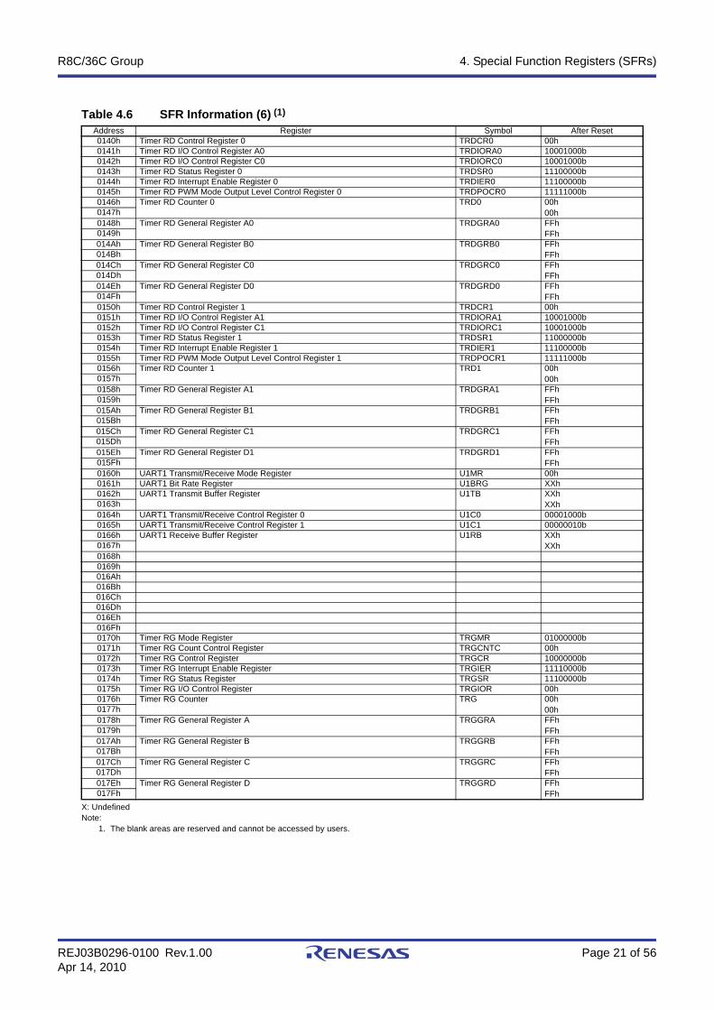
Table 4.6 SFR Information (6) (1)
X: UndefinedNote:
1. The blank areas are reserved and cannot be accessed by users.
Address Register Symbol After Reset0140h Timer RD Control Register 0 TRDCR0 00h0141h Timer RD I/O Control Register A0 TRDIORA0 10001000b0142h Timer RD I/O Control Register C0 TRDIORC0 10001000b0143h Timer RD Status Register 0 TRDSR0 11100000b0144h Timer RD Interrupt Enable Register 0 TRDIER0 11100000b0145h Timer RD PWM Mode Output Level Control Register 0 TRDPOCR0 11111000b0146h Timer RD Counter 0 TRD0 00h
00h0147h0148h Timer RD General Register A0 TRDGRA0 FFh
FFh0149h014Ah Timer RD General Register B0 TRDGRB0 FFh
FFh014Bh014Ch Timer RD General Register C0 TRDGRC0 FFh
FFh014Dh014Eh Timer RD General Register D0 TRDGRD0 FFh
FFh014Fh0150h Timer RD Control Register 1 TRDCR1 00h0151h Timer RD I/O Control Register A1 TRDIORA1 10001000b0152h Timer RD I/O Control Register C1 TRDIORC1 10001000b0153h Timer RD Status Register 1 TRDSR1 11000000b0154h Timer RD Interrupt Enable Register 1 TRDIER1 11100000b0155h Timer RD PWM Mode Output Level Control Register 1 TRDPOCR1 11111000b0156h Timer RD Counter 1 TRD1 00h
00h0157h0158h Timer RD General Register A1 TRDGRA1 FFh
FFh0159h015Ah Timer RD General Register B1 TRDGRB1 FFh
FFh015Bh015Ch Timer RD General Register C1 TRDGRC1 FFh
FFh015Dh015Eh Timer RD General Register D1 TRDGRD1 FFh
FFh015Fh0160h UART1 Transmit/Receive Mode Register U1MR 00h0161h UART1 Bit Rate Register U1BRG XXh0162h UART1 Transmit Buffer Register U1TB XXh
XXh0163h0164h UART1 Transmit/Receive Control Register 0 U1C0 00001000b0165h UART1 Transmit/Receive Control Register 1 U1C1 00000010b0166h UART1 Receive Buffer Register U1RB XXh
XXh0167h0168h0169h016Ah016Bh016Ch016Dh016Eh016Fh0170h Timer RG Mode Register TRGMR 01000000b0171h Timer RG Count Control Register TRGCNTC 00h0172h Timer RG Control Register TRGCR 10000000b0173h Timer RG Interrupt Enable Register TRGIER 11110000b0174h Timer RG Status Register TRGSR 11100000b0175h Timer RG I/O Control Register TRGIOR 00h0176h Timer RG Counter TRG 00h
00h0177h0178h Timer RG General Register A TRGGRA FFh
FFh0179h017Ah Timer RG General Register B TRGGRB FFh
FFh017Bh017Ch Timer RG General Register C TRGGRC FFh
FFh017Dh017Eh Timer RG General Register D TRGGRD FFh
FFh017Fh
R8C/36C Group 4. Special Function Registers (SFRs)
REJ03B0296-0100 Rev.1.00 Page 22 of 56Apr 14, 2010
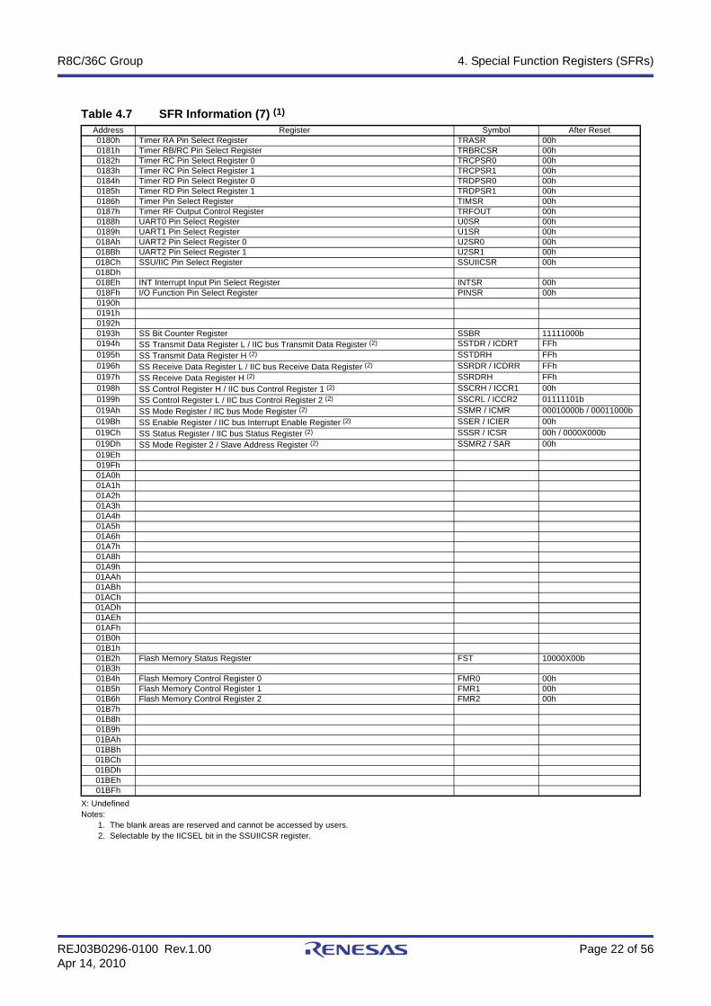
Table 4.7 SFR Information (7) (1)
X: UndefinedNotes:
1. The blank areas are reserved and cannot be accessed by users.2. Selectable by the IICSEL bit in the SSUIICSR register.
Address Register Symbol After Reset0180h Timer RA Pin Select Register TRASR 00h0181h Timer RB/RC Pin Select Register TRBRCSR 00h0182h Timer RC Pin Select Register 0 TRCPSR0 00h0183h Timer RC Pin Select Register 1 TRCPSR1 00h0184h Timer RD Pin Select Register 0 TRDPSR0 00h0185h Timer RD Pin Select Register 1 TRDPSR1 00h0186h Timer Pin Select Register TIMSR 00h0187h Timer RF Output Control Register TRFOUT 00h0188h UART0 Pin Select Register U0SR 00h0189h UART1 Pin Select Register U1SR 00h018Ah UART2 Pin Select Register 0 U2SR0 00h018Bh UART2 Pin Select Register 1 U2SR1 00h018Ch SSU/IIC Pin Select Register SSUIICSR 00h018Dh018Eh INT Interrupt Input Pin Select Register INTSR 00h018Fh I/O Function Pin Select Register PINSR 00h0190h0191h0192h0193h SS Bit Counter Register SSBR 11111000b0194h SS Transmit Data Register L / IIC bus Transmit Data Register (2) SSTDR / ICDRT FFh0195h SS Transmit Data Register H (2) SSTDRH FFh0196h SS Receive Data Register L / IIC bus Receive Data Register (2) SSRDR / ICDRR FFh0197h SS Receive Data Register H (2) SSRDRH FFh0198h SS Control Register H / IIC bus Control Register 1 (2) SSCRH / ICCR1 00h0199h SS Control Register L / IIC bus Control Register 2 (2) SSCRL / ICCR2 01111101b019Ah SS Mode Register / IIC bus Mode Register (2) SSMR / ICMR 00010000b / 00011000b019Bh SS Enable Register / IIC bus Interrupt Enable Register (2) SSER / ICIER 00h019Ch SS Status Register / IIC bus Status Register (2) SSSR / ICSR 00h / 0000X000b019Dh SS Mode Register 2 / Slave Address Register (2) SSMR2 / SAR 00h019Eh019Fh01A0h01A1h01A2h01A3h01A4h01A5h01A6h01A7h01A8h01A9h01AAh01ABh01ACh01ADh01AEh01AFh01B0h01B1h01B2h Flash Memory Status Register FST 10000X00b01B3h01B4h Flash Memory Control Register 0 FMR0 00h01B5h Flash Memory Control Register 1 FMR1 00h01B6h Flash Memory Control Register 2 FMR2 00h01B7h01B8h01B9h01BAh01BBh01BCh01BDh01BEh01BFh
R8C/36C Group 4. Special Function Registers (SFRs)
REJ03B0296-0100 Rev.1.00 Page 23 of 56Apr 14, 2010
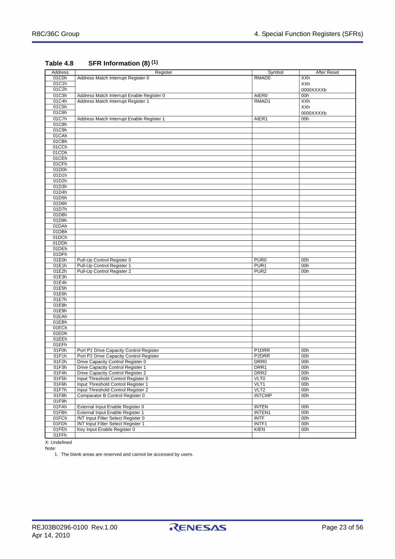
Table 4.8 SFR Information (8) (1)
X: UndefinedNote:
1. The blank areas are reserved and cannot be accessed by users.
Address Register Symbol After Reset01C0h Address Match Interrupt Register 0 RMAD0 XXh
XXh0000XXXXb
01C1h01C2h01C3h Address Match Interrupt Enable Register 0 AIER0 00h01C4h Address Match Interrupt Register 1 RMAD1 XXh
XXh0000XXXXb
01C5h01C6h01C7h Address Match Interrupt Enable Register 1 AIER1 00h01C8h01C9h01CAh01CBh01CCh01CDh01CEh01CFh01D0h01D1h01D2h01D3h01D4h01D5h01D6h01D7h01D8h01D9h01DAh01DBh01DCh01DDh01DEh01DFh01E0h Pull-Up Control Register 0 PUR0 00h01E1h Pull-Up Control Register 1 PUR1 00h01E2h Pull-Up Control Register 2 PUR2 00h01E3h01E4h01E5h01E6h01E7h01E8h01E9h01EAh01EBh01ECh01EDh01EEh01EFh01F0h Port P1 Drive Capacity Control Register P1DRR 00h01F1h Port P2 Drive Capacity Control Register P2DRR 00h01F2h Drive Capacity Control Register 0 DRR0 00h01F3h Drive Capacity Control Register 1 DRR1 00h01F4h Drive Capacity Control Register 2 DRR2 00h01F5h Input Threshold Control Register 0 VLT0 00h01F6h Input Threshold Control Register 1 VLT1 00h01F7h Input Threshold Control Register 2 VLT2 00h01F8h Comparator B Control Register 0 INTCMP 00h01F9h01FAh External Input Enable Register 0 INTEN 00h01FBh External Input Enable Register 1 INTEN1 00h01FCh INT Input Filter Select Register 0 INTF 00h01FDh INT Input Filter Select Register 1 INTF1 00h01FEh Key Input Enable Register 0 KIEN 00h01FFh
R8C/36C Group 4. Special Function Registers (SFRs)
REJ03B0296-0100 Rev.1.00 Page 24 of 56Apr 14, 2010
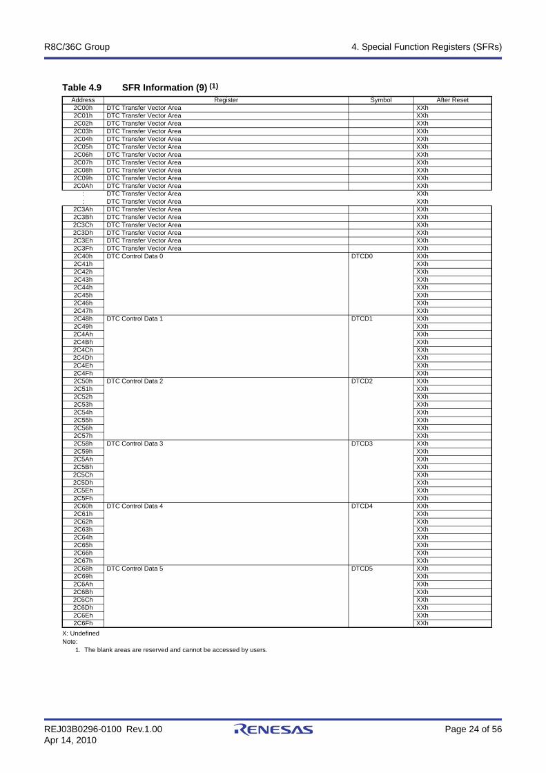
Table 4.9 SFR Information (9) (1)
X: UndefinedNote:
1. The blank areas are reserved and cannot be accessed by users.
Address Register Symbol After Reset2C00h DTC Transfer Vector Area XXh2C01h DTC Transfer Vector Area XXh2C02h DTC Transfer Vector Area XXh2C03h DTC Transfer Vector Area XXh2C04h DTC Transfer Vector Area XXh2C05h DTC Transfer Vector Area XXh2C06h DTC Transfer Vector Area XXh2C07h DTC Transfer Vector Area XXh2C08h DTC Transfer Vector Area XXh2C09h DTC Transfer Vector Area XXh2C0Ah DTC Transfer Vector Area XXh
: DTC Transfer Vector Area XXh: DTC Transfer Vector Area XXh
2C3Ah DTC Transfer Vector Area XXh2C3Bh DTC Transfer Vector Area XXh2C3Ch DTC Transfer Vector Area XXh2C3Dh DTC Transfer Vector Area XXh2C3Eh DTC Transfer Vector Area XXh2C3Fh DTC Transfer Vector Area XXh2C40h DTC Control Data 0 DTCD0 XXh2C41h XXh2C42h XXh2C43h XXh2C44h XXh2C45h XXh2C46h XXh2C47h XXh2C48h DTC Control Data 1 DTCD1 XXh2C49h XXh2C4Ah XXh2C4Bh XXh2C4Ch XXh2C4Dh XXh2C4Eh XXh2C4Fh XXh2C50h DTC Control Data 2 DTCD2 XXh2C51h XXh2C52h XXh2C53h XXh2C54h XXh2C55h XXh2C56h XXh2C57h XXh2C58h DTC Control Data 3 DTCD3 XXh2C59h XXh2C5Ah XXh2C5Bh XXh2C5Ch XXh2C5Dh XXh2C5Eh XXh2C5Fh XXh2C60h DTC Control Data 4 DTCD4 XXh2C61h XXh2C62h XXh2C63h XXh2C64h XXh2C65h XXh2C66h XXh2C67h XXh2C68h DTC Control Data 5 DTCD5 XXh2C69h XXh2C6Ah XXh2C6Bh XXh2C6Ch XXh2C6Dh XXh2C6Eh XXh2C6Fh XXh
R8C/36C Group 4. Special Function Registers (SFRs)
REJ03B0296-0100 Rev.1.00 Page 25 of 56Apr 14, 2010
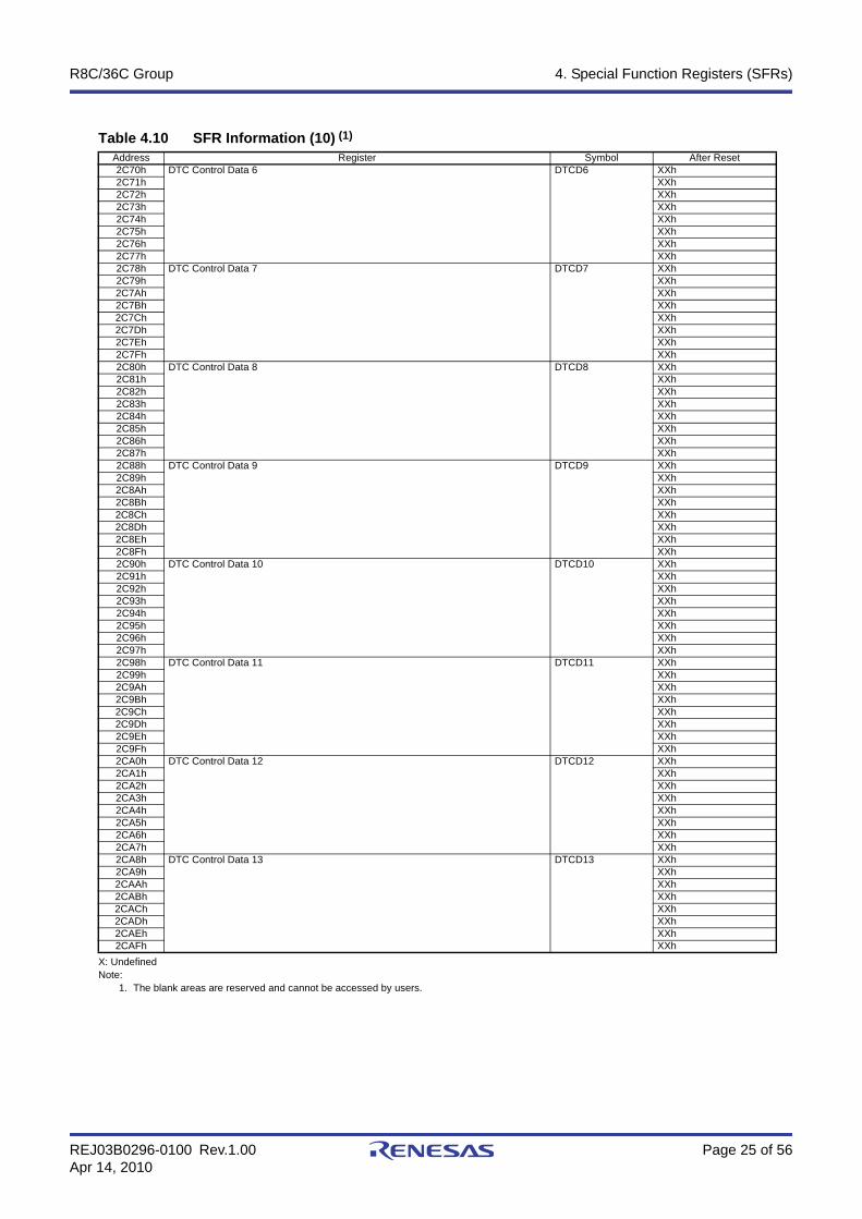
Table 4.10 SFR Information (10) (1)
X: UndefinedNote:
1. The blank areas are reserved and cannot be accessed by users.
Address Register Symbol After Reset2C70h DTC Control Data 6 DTCD6 XXh2C71h XXh2C72h XXh2C73h XXh2C74h XXh2C75h XXh2C76h XXh2C77h XXh2C78h DTC Control Data 7 DTCD7 XXh2C79h XXh2C7Ah XXh2C7Bh XXh2C7Ch XXh2C7Dh XXh2C7Eh XXh2C7Fh XXh2C80h DTC Control Data 8 DTCD8 XXh2C81h XXh2C82h XXh2C83h XXh2C84h XXh2C85h XXh2C86h XXh2C87h XXh2C88h DTC Control Data 9 DTCD9 XXh2C89h XXh2C8Ah XXh2C8Bh XXh2C8Ch XXh2C8Dh XXh2C8Eh XXh2C8Fh XXh2C90h DTC Control Data 10 DTCD10 XXh2C91h XXh2C92h XXh2C93h XXh2C94h XXh2C95h XXh2C96h XXh2C97h XXh2C98h DTC Control Data 11 DTCD11 XXh2C99h XXh2C9Ah XXh2C9Bh XXh2C9Ch XXh2C9Dh XXh2C9Eh XXh2C9Fh XXh2CA0h DTC Control Data 12 DTCD12 XXh2CA1h XXh2CA2h XXh2CA3h XXh2CA4h XXh2CA5h XXh2CA6h XXh2CA7h XXh2CA8h DTC Control Data 13 DTCD13 XXh2CA9h XXh2CAAh XXh2CABh XXh2CACh XXh2CADh XXh2CAEh XXh2CAFh XXh
R8C/36C Group 4. Special Function Registers (SFRs)
REJ03B0296-0100 Rev.1.00 Page 26 of 56Apr 14, 2010
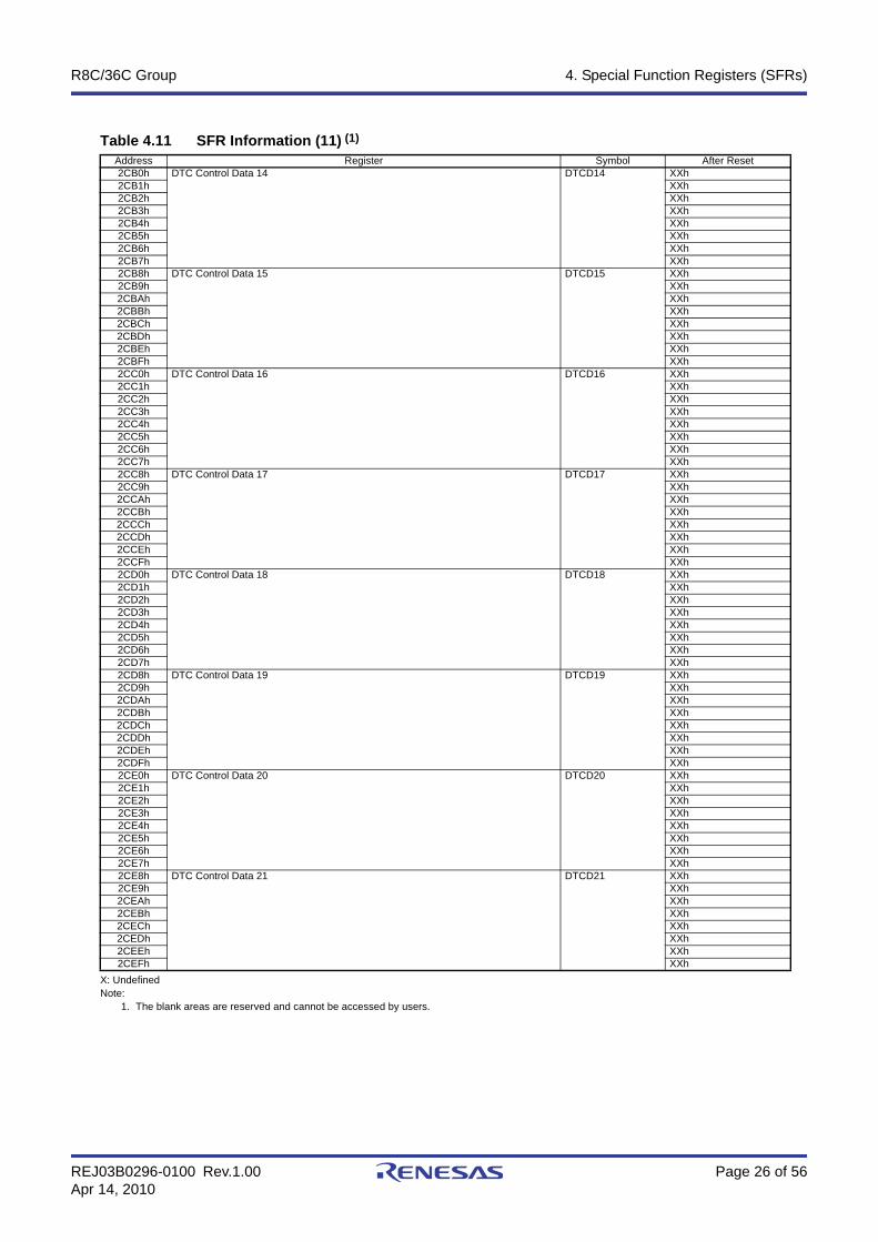
Table 4.11 SFR Information (11) (1)
X: UndefinedNote:
1. The blank areas are reserved and cannot be accessed by users.
Address Register Symbol After Reset2CB0h DTC Control Data 14 DTCD14 XXh2CB1h XXh2CB2h XXh2CB3h XXh2CB4h XXh2CB5h XXh2CB6h XXh2CB7h XXh2CB8h DTC Control Data 15 DTCD15 XXh2CB9h XXh2CBAh XXh2CBBh XXh2CBCh XXh2CBDh XXh2CBEh XXh2CBFh XXh2CC0h DTC Control Data 16 DTCD16 XXh2CC1h XXh2CC2h XXh2CC3h XXh2CC4h XXh2CC5h XXh2CC6h XXh2CC7h XXh2CC8h DTC Control Data 17 DTCD17 XXh2CC9h XXh2CCAh XXh2CCBh XXh2CCCh XXh2CCDh XXh2CCEh XXh2CCFh XXh2CD0h DTC Control Data 18 DTCD18 XXh2CD1h XXh2CD2h XXh2CD3h XXh2CD4h XXh2CD5h XXh2CD6h XXh2CD7h XXh2CD8h DTC Control Data 19 DTCD19 XXh2CD9h XXh2CDAh XXh2CDBh XXh2CDCh XXh2CDDh XXh2CDEh XXh2CDFh XXh2CE0h DTC Control Data 20 DTCD20 XXh2CE1h XXh2CE2h XXh2CE3h XXh2CE4h XXh2CE5h XXh2CE6h XXh2CE7h XXh2CE8h DTC Control Data 21 DTCD21 XXh2CE9h XXh2CEAh XXh2CEBh XXh2CECh XXh2CEDh XXh2CEEh XXh2CEFh XXh
R8C/36C Group 4. Special Function Registers (SFRs)
REJ03B0296-0100 Rev.1.00 Page 27 of 56Apr 14, 2010
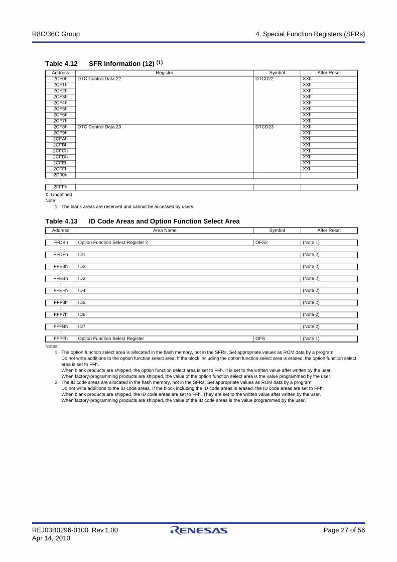
Table 4.12 SFR Information (12) (1)
X: UndefinedNote:
1. The blank areas are reserved and cannot be accessed by users.
Table 4.13 ID Code Areas and Option Function Select Area
Notes:1. The option function select area is allocated in the flash memory, not in the SFRs. Set appropriate values as ROM data by a program.
Do not write additions to the option function select area. If the block including the option function select area is erased, the option function select area is set to FFh.When blank products are shipped, the option function select area is set to FFh. It is set to the written value after written by the user.When factory-programming products are shipped, the value of the option function select area is the value programmed by the user.
2. The ID code areas are allocated in the flash memory, not in the SFRs. Set appropriate values as ROM data by a program.Do not write additions to the ID code areas. If the block including the ID code areas is erased, the ID code areas are set to FFh.When blank products are shipped, the ID code areas are set to FFh. They are set to the written value after written by the user.When factory-programming products are shipped, the value of the ID code areas is the value programmed by the user.
Address Register Symbol After Reset2CF0h DTC Control Data 22 DTCD22 XXh2CF1h XXh2CF2h XXh2CF3h XXh2CF4h XXh2CF5h XXh2CF6h XXh2CF7h XXh2CF8h DTC Control Data 23 DTCD23 XXh2CF9h XXh2CFAh XXh2CFBh XXh2CFCh XXh2CFDh XXh2CFEh XXh2CFFh XXh2D00h
:2FFFh
Address Area Name Symbol After Reset:
FFDBh Option Function Select Register 2 OFS2 (Note 1):
FFDFh ID1 (Note 2):
FFE3h ID2 (Note 2):
FFEBh ID3 (Note 2):
FFEFh ID4 (Note 2):
FFF3h ID5 (Note 2):
FFF7h ID6 (Note 2):
FFFBh ID7 (Note 2):
FFFFh Option Function Select Register OFS (Note 1)
R8C/36C Group 5. Electrical Characteristics
REJ03B0296-0100 Rev.1.00 Page 28 of 56Apr 14, 2010
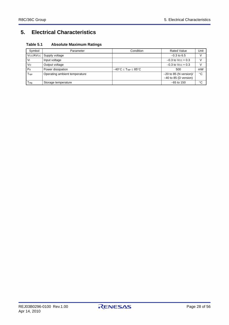
5. Electrical Characteristics
Table 5.1 Absolute Maximum RatingsSymbol Parameter Condition Rated Value Unit
VCC/AVCC Supply voltage −0.3 to 6.5 VVI Input voltage −0.3 to VCC + 0.3 VVO Output voltage −0.3 to VCC + 0.3 VPd Power dissipation −40°C ≤ Topr ≤ 85°C 500 mWTopr Operating ambient temperature −20 to 85 (N version)/
−40 to 85 (D version)°C
Tstg Storage temperature −65 to 150 °C
R8C/36C Group 5. Electrical Characteristics
REJ03B0296-0100 Rev.1.00 Page 29 of 56Apr 14, 2010
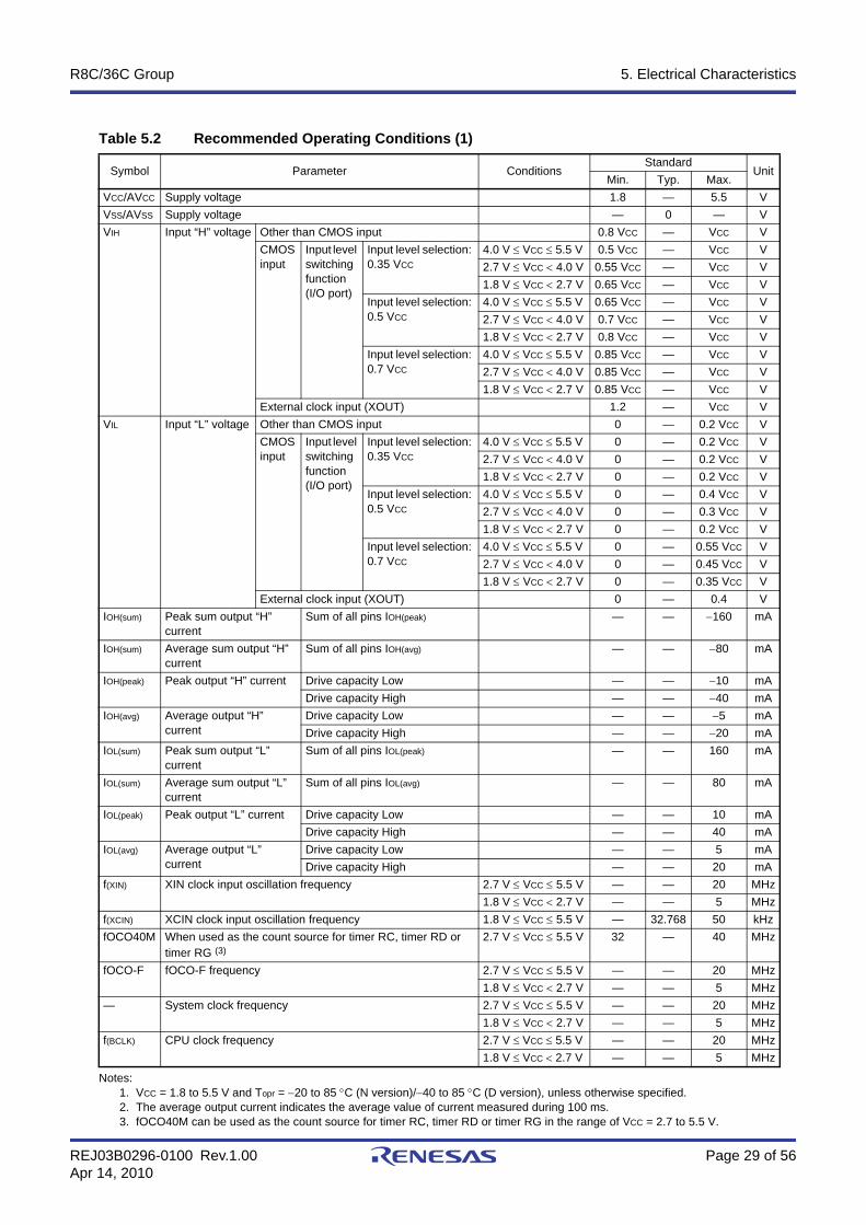
Notes:1. VCC = 1.8 to 5.5 V and Topr = −20 to 85 °C (N version)/−40 to 85 °C (D version), unless otherwise specified.2. The average output current indicates the average value of current measured during 100 ms.3. fOCO40M can be used as the count source for timer RC, timer RD or timer RG in the range of VCC = 2.7 to 5.5 V.
Table 5.2 Recommended Operating Conditions (1)
Symbol Parameter ConditionsStandard
UnitMin. Typ. Max.
VCC/AVCC Supply voltage 1.8 — 5.5 VVSS/AVSS Supply voltage — 0 — VVIH Input “H” voltage Other than CMOS input 0.8 VCC — VCC V
CMOS input
Input level switching function (I/O port)
Input level selection: 0.35 VCC
4.0 V ≤ VCC ≤ 5.5 V 0.5 VCC — VCC V2.7 V ≤ VCC < 4.0 V 0.55 VCC — VCC V1.8 V ≤ VCC < 2.7 V 0.65 VCC — VCC V
Input level selection: 0.5 VCC
4.0 V ≤ VCC ≤ 5.5 V 0.65 VCC — VCC V2.7 V ≤ VCC < 4.0 V 0.7 VCC — VCC V1.8 V ≤ VCC < 2.7 V 0.8 VCC — VCC V
Input level selection: 0.7 VCC
4.0 V ≤ VCC ≤ 5.5 V 0.85 VCC — VCC V2.7 V ≤ VCC < 4.0 V 0.85 VCC — VCC V1.8 V ≤ VCC < 2.7 V 0.85 VCC — VCC V
External clock input (XOUT) 1.2 — VCC VVIL Input “L” voltage Other than CMOS input 0 — 0.2 VCC V
CMOS input
Input level switching function (I/O port)
Input level selection: 0.35 VCC
4.0 V ≤ VCC ≤ 5.5 V 0 — 0.2 VCC V2.7 V ≤ VCC < 4.0 V 0 — 0.2 VCC V1.8 V ≤ VCC < 2.7 V 0 — 0.2 VCC V
Input level selection: 0.5 VCC
4.0 V ≤ VCC ≤ 5.5 V 0 — 0.4 VCC V2.7 V ≤ VCC < 4.0 V 0 — 0.3 VCC V1.8 V ≤ VCC < 2.7 V 0 — 0.2 VCC V
Input level selection: 0.7 VCC
4.0 V ≤ VCC ≤ 5.5 V 0 — 0.55 VCC V2.7 V ≤ VCC < 4.0 V 0 — 0.45 VCC V1.8 V ≤ VCC < 2.7 V 0 — 0.35 VCC V
External clock input (XOUT) 0 — 0.4 VIOH(sum) Peak sum output “H”
currentSum of all pins IOH(peak) — — −160 mA
IOH(sum) Average sum output “H” current
Sum of all pins IOH(avg) — — −80 mA
IOH(peak) Peak output “H” current Drive capacity Low — — −10 mADrive capacity High — — −40 mA
IOH(avg) Average output “H” current
Drive capacity Low — — −5 mADrive capacity High — — −20 mA
IOL(sum) Peak sum output “L” current
Sum of all pins IOL(peak) — — 160 mA
IOL(sum) Average sum output “L” current
Sum of all pins IOL(avg) — — 80 mA
IOL(peak) Peak output “L” current Drive capacity Low — — 10 mADrive capacity High — — 40 mA
IOL(avg) Average output “L” current
Drive capacity Low — — 5 mADrive capacity High — — 20 mA
f(XIN) XIN clock input oscillation frequency 2.7 V ≤ VCC ≤ 5.5 V — — 20 MHz1.8 V ≤ VCC < 2.7 V — — 5 MHz
f(XCIN) XCIN clock input oscillation frequency 1.8 V ≤ VCC ≤ 5.5 V — 32.768 50 kHzfOCO40M When used as the count source for timer RC, timer RD or
timer RG (3)2.7 V ≤ VCC ≤ 5.5 V 32 — 40 MHz
fOCO-F fOCO-F frequency 2.7 V ≤ VCC ≤ 5.5 V — — 20 MHz1.8 V ≤ VCC < 2.7 V — — 5 MHz
— System clock frequency 2.7 V ≤ VCC ≤ 5.5 V — — 20 MHz1.8 V ≤ VCC < 2.7 V — — 5 MHz
f(BCLK) CPU clock frequency 2.7 V ≤ VCC ≤ 5.5 V — — 20 MHz1.8 V ≤ VCC < 2.7 V — — 5 MHz
R8C/36C Group 5. Electrical Characteristics
REJ03B0296-0100 Rev.1.00 Page 30 of 56Apr 14, 2010
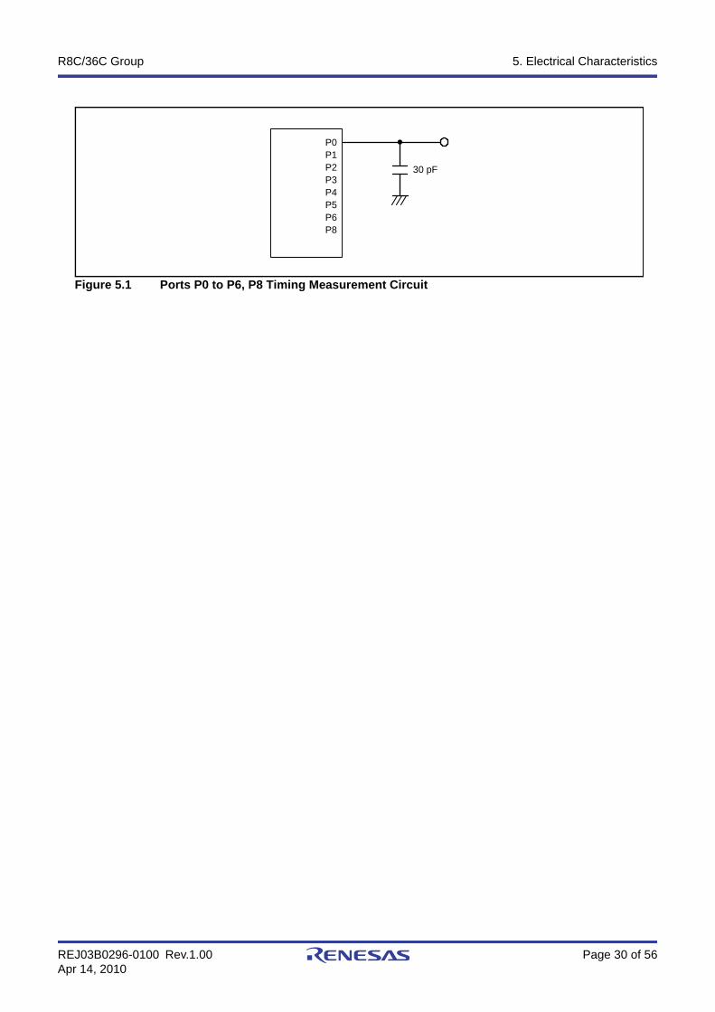
Figure 5.1 Ports P0 to P6, P8 Timing Measurement Circuit
P0P1P2P3P4P5P6P8
30 pF
R8C/36C Group 5. Electrical Characteristics
REJ03B0296-0100 Rev.1.00 Page 31 of 56Apr 14, 2010
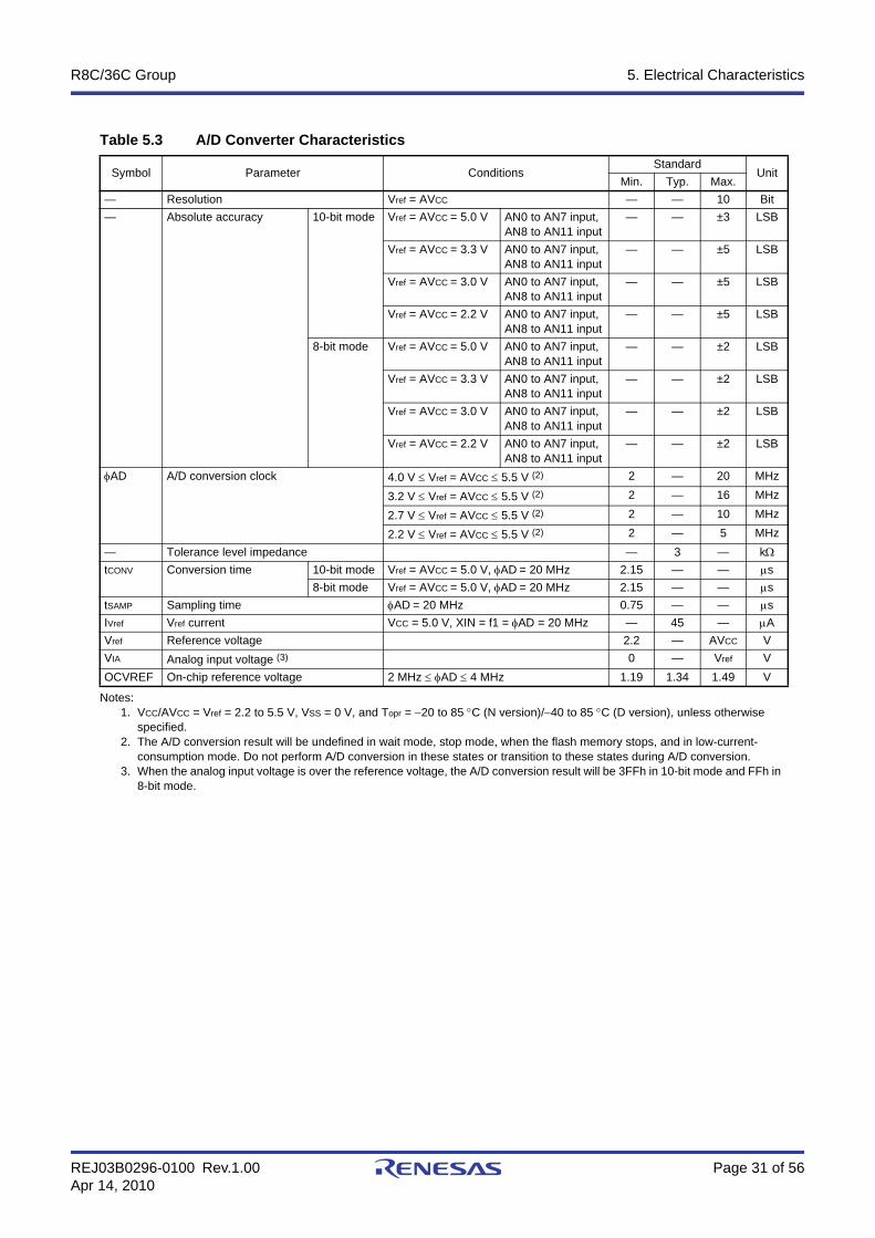
Notes:1. VCC/AVCC = Vref = 2.2 to 5.5 V, VSS = 0 V, and Topr = −20 to 85 °C (N version)/−40 to 85 °C (D version), unless otherwise
specified.2. The A/D conversion result will be undefined in wait mode, stop mode, when the flash memory stops, and in low-current-
consumption mode. Do not perform A/D conversion in these states or transition to these states during A/D conversion.3. When the analog input voltage is over the reference voltage, the A/D conversion result will be 3FFh in 10-bit mode and FFh in
8-bit mode.
Table 5.3 A/D Converter Characteristics
Symbol Parameter ConditionsStandard
UnitMin. Typ. Max.
— Resolution Vref = AVCC — — 10 Bit— Absolute accuracy 10-bit mode Vref = AVCC = 5.0 V AN0 to AN7 input,
AN8 to AN11 input— — ±3 LSB
Vref = AVCC = 3.3 V AN0 to AN7 input, AN8 to AN11 input
— — ±5 LSB
Vref = AVCC = 3.0 V AN0 to AN7 input, AN8 to AN11 input
— — ±5 LSB
Vref = AVCC = 2.2 V AN0 to AN7 input, AN8 to AN11 input
— — ±5 LSB
8-bit mode Vref = AVCC = 5.0 V AN0 to AN7 input, AN8 to AN11 input
— — ±2 LSB
Vref = AVCC = 3.3 V AN0 to AN7 input, AN8 to AN11 input
— — ±2 LSB
Vref = AVCC = 3.0 V AN0 to AN7 input, AN8 to AN11 input
— — ±2 LSB
Vref = AVCC = 2.2 V AN0 to AN7 input, AN8 to AN11 input
— — ±2 LSB
φAD A/D conversion clock 4.0 V ≤ Vref = AVCC ≤ 5.5 V (2) 2 — 20 MHz
3.2 V ≤ Vref = AVCC ≤ 5.5 V (2) 2 — 16 MHz
2.7 V ≤ Vref = AVCC ≤ 5.5 V (2) 2 — 10 MHz
2.2 V ≤ Vref = AVCC ≤ 5.5 V (2) 2 — 5 MHz— Tolerance level impedance — 3 — kΩtCONV Conversion time 10-bit mode Vref = AVCC = 5.0 V, φAD = 20 MHz 2.15 — — µs
8-bit mode Vref = AVCC = 5.0 V, φAD = 20 MHz 2.15 — — µstSAMP Sampling time φAD = 20 MHz 0.75 — — µsIVref Vref current VCC = 5.0 V, XIN = f1 = φAD = 20 MHz — 45 — µAVref Reference voltage 2.2 — AVCC VVIA Analog input voltage (3) 0 — Vref VOCVREF On-chip reference voltage 2 MHz ≤ φAD ≤ 4 MHz 1.19 1.34 1.49 V
R8C/36C Group 5. Electrical Characteristics
REJ03B0296-0100 Rev.1.00 Page 32 of 56Apr 14, 2010
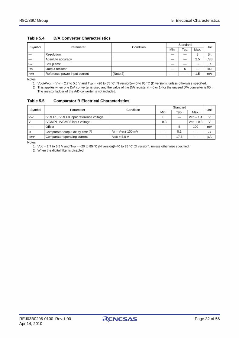
Notes:1. VCC/AVCC = Vref = 2.7 to 5.5 V and Topr = −20 to 85 °C (N version)/−40 to 85 °C (D version), unless otherwise specified.2. This applies when one D/A converter is used and the value of the DAi register (i = 0 or 1) for the unused D/A converter is 00h.
The resistor ladder of the A/D converter is not included.
Notes:1. VCC = 2.7 to 5.5 V and Topr = −20 to 85 °C (N version)/−40 to 85 °C (D version), unless otherwise specified.2. When the digital filter is disabled.
Table 5.4 D/A Converter Characteristics
Symbol Parameter ConditionStandard
UnitMin. Typ. Max.
— Resolution — — 8 Bit— Absolute accuracy — — 2.5 LSBtsu Setup time — — 3 µsRO Output resistor — 6 — kΩIVref Reference power input current (Note 2) — — 1.5 mA
Table 5.5 Comparator B Electrical Characteristics
Symbol Parameter ConditionStandard
UnitMin. Typ. Max.
Vref IVREF1, IVREF3 input reference voltage 0 — VCC − 1.4 VVI IVCMP1, IVCMP3 input voltage −0.3 — VCC + 0.3 V— Offset — 5 100 mVtd Comparator output delay time (2) VI = Vref ± 100 mV — 0.1 — µsICMP Comparator operating current VCC = 5.0 V — 17.5 — µA
R8C/36C Group 5. Electrical Characteristics
REJ03B0296-0100 Rev.1.00 Page 33 of 56Apr 14, 2010
Notes:1. VCC = 2.7 to 5.5 V and Topr = 0 to 60 °C, unless otherwise specified.2. Definition of programming/erasure endurance
The programming and erasure endurance is defined on a per-block basis. If the programming and erasure endurance is n (n = 1,000), each block can be erased n times. For example, if 1,024 1-byte writes are performed to different addresses in block A, a 1 Kbyte block, and then the block is erased, the programming/erasure endurance still stands at one. However, the same address must not be programmed more than once per erase operation (overwriting prohibited).
3. Endurance to guarantee all electrical characteristics after program and erase. (1 to Min. value can be guaranteed.)4. In a system that executes multiple programming operations, the actual erasure count can be reduced by writing to sequential
addresses in turn so that as much of the block as possible is used up before performing an erase operation. For example, when programming groups of 16 bytes, the effective number of rewrites can be minimized by programming up to 128 groups before erasing them all in one operation. It is also advisable to retain data on the erasure endurance of each block and limit the number of erase operations to a certain number.
5. If an error occurs during block erase, attempt to execute the clear status register command, then execute the block erase command at least three times until the erase error does not occur.
6. Customers desiring program/erase failure rate information should contact their Renesas technical support representative.7. The data hold time includes time that the power supply is off or the clock is not supplied.
Table 5.6 Flash Memory (Program ROM) Electrical Characteristics
Symbol Parameter ConditionsStandard
UnitMin. Typ. Max.
— Program/erase endurance (2) 1,000 (3) — — times— Byte program time — 80 500 µs— Block erase time — 0.3 — std(SR-SUS) Time delay from suspend request until
suspend— — 5 + CPU clock
× 3 cyclesms
— Interval from erase start/restart until following suspend request
0 — — µs
— Time from suspend until erase restart — — 30 + CPU clock × 1 cycle
µs
td(CMDRST-READY)
Time from when command is forcibly stopped until reading is enabled
— — 30 + CPU clock × 1 cycle
µs
— Program, erase voltage 2.7 — 5.5 V— Read voltage 1.8 — 5.5 V— Program, erase temperature 0 — 60 °C— Data hold time (7) Ambient temperature = 55 °C 20 — — year
R8C/36C Group 5. Electrical Characteristics
REJ03B0296-0100 Rev.1.00 Page 34 of 56Apr 14, 2010
Notes:1. VCC = 2.7 to 5.5 V and Topr = −20 to 85 °C (N version)/−40 to 85 °C (D version), unless otherwise specified.2. Definition of programming/erasure endurance
The programming and erasure endurance is defined on a per-block basis. If the programming and erasure endurance is n (n = 10,000), each block can be erased n times. For example, if 1,024 1-byte writes are performed to different addresses in block A, a 1 Kbyte block, and then the block is erased, the programming/erasure endurance still stands at one. However, the same address must not be programmed more than once per erase operation (overwriting prohibited).
3. Endurance to guarantee all electrical characteristics after program and erase. (1 to Min. value can be guaranteed.)4. In a system that executes multiple programming operations, the actual erasure count can be reduced by writing to sequential
addresses in turn so that as much of the block as possible is used up before performing an erase operation. For example, when programming groups of 16 bytes, the effective number of rewrites can be minimized by programming up to 128 groups before erasing them all in one operation. In addition, averaging the erasure endurance between blocks A to D can further reduce the actual erasure endurance. It is also advisable to retain data on the erasure endurance of each block and limit the number of erase operations to a certain number.
5. If an error occurs during block erase, attempt to execute the clear status register command, then execute the block erase command at least three times until the erase error does not occur.
6. Customers desiring program/erase failure rate information should contact their Renesas technical support representative.7. −40 °C for D version.8. The data hold time includes time that the power supply is off or the clock is not supplied.
Figure 5.2 Time delay until Suspend
Table 5.7 Flash Memory (Data flash Block A to Block D) Electrical Characteristics
Symbol Parameter ConditionsStandard
UnitMin. Typ. Max.
— Program/erase endurance (2) 10,000 (3) — — times— Byte program time
(program/erase endurance ≤ 1,000 times)— 160 1500 µs
— Byte program time(program/erase endurance > 1,000 times)
— 300 1500 µs
— Block erase time(program/erase endurance ≤ 1,000 times)
— 0.2 1 s
— Block erase time(program/erase endurance > 1,000 times)
— 0.3 1 s
td(SR-SUS) Time delay from suspend request until suspend
— — 5 + CPU clock × 3 cycles
ms
— Interval from erase start/restart until following suspend request
0 — — µs
— Time from suspend until erase restart — — 30 + CPU clock × 1 cycle
µs
td(CMDRST-READY)
Time from when command is forcibly stopped until reading is enabled
— — 30 + CPU clock × 1 cycle
µs
— Program, erase voltage 2.7 — 5.5 V— Read voltage 1.8 — 5.5 V— Program, erase temperature −20 (7) — 85 °C— Data hold time (8) Ambient temperature = 55 °C 20 — — year
FST6 bit
Suspend request(FMR21 bit)
Fixed time
td(SR-SUS)
Clock-dependenttime
Access restart
FST6, FST7: Bit in FST registerFMR21: Bit in FMR2 register
FST7 bit
R8C/36C Group 5. Electrical Characteristics
REJ03B0296-0100 Rev.1.00 Page 35 of 56Apr 14, 2010
Notes:1. The measurement condition is VCC = 1.8 to 5.5 V and Topr = −20 to 85 °C (N version)/−40 to 85 °C (D version).2. Select the voltage detection level with bits VDSEL0 and VDSEL1 in the OFS register. 3. Necessary time until the voltage detection circuit operates when setting to 1 again after setting the VCA25 bit in the VCA2
register to 0.4. Time until the voltage monitor 0 reset is generated after the voltage passes Vdet0.
Notes:1. The measurement condition is VCC = 1.8 to 5.5 V and Topr = −20 to 85 °C (N version)/−40 to 85 °C (D version).2. Select the voltage detection level with bits VD1S0 to VD1S3 in the VD1LS register.3. Time until the voltage monitor 1 interrupt request is generated after the voltage passes Vdet1.4. Necessary time until the voltage detection circuit operates when setting to 1 again after setting the VCA26 bit in the VCA2
register to 0.
Table 5.8 Voltage Detection 0 Circuit Electrical Characteristics
Symbol Parameter ConditionStandard
UnitMin. Typ. Max.
Vdet0 Voltage detection level Vdet0_0 (2) 1.80 1.90 2.05 V
Voltage detection level Vdet0_1 (2) 2.15 2.35 2.50 V
Voltage detection level Vdet0_2 (2) 2.70 2.85 3.05 V
Voltage detection level Vdet0_3 (2) 3.55 3.80 4.05 V— Voltage detection 0 circuit response time (4) At the falling of VCC from
5.0 V to (Vdet0_0 − 0.1) V— 6 150 µs
— Voltage detection circuit self power consumption VCA25 = 1, VCC = 5.0 V — 1.5 — µAtd(E-A) Waiting time until voltage detection circuit operation
starts (3)— — 100 µs
Table 5.9 Voltage Detection 1 Circuit Electrical Characteristics
Symbol Parameter ConditionStandard
UnitMin. Typ. Max.
Vdet1 Voltage detection level Vdet1_0 (2) At the falling of VCC 2.00 2.20 2.40 V
Voltage detection level Vdet1_1 (2) At the falling of VCC 2.15 2.35 2.55 V
Voltage detection level Vdet1_2 (2) At the falling of VCC 2.30 2.50 2.70 V
Voltage detection level Vdet1_3 (2) At the falling of VCC 2.45 2.65 2.85 V
Voltage detection level Vdet1_4 (2) At the falling of VCC 2.60 2.80 3.00 V
Voltage detection level Vdet1_5 (2) At the falling of VCC 2.75 2.95 3.15 V
Voltage detection level Vdet1_6 (2) At the falling of VCC 2.85 3.10 3.40 V
Voltage detection level Vdet1_7 (2) At the falling of VCC 3.00 3.25 3.55 V
Voltage detection level Vdet1_8 (2) At the falling of VCC 3.15 3.40 3.70 V
Voltage detection level Vdet1_9 (2) At the falling of VCC 3.30 3.55 3.85 V
Voltage detection level Vdet1_A (2) At the falling of VCC 3.45 3.70 4.00 V
Voltage detection level Vdet1_B (2) At the falling of VCC 3.60 3.85 4.15 V
Voltage detection level Vdet1_C (2) At the falling of VCC 3.75 4.00 4.30 V
Voltage detection level Vdet1_D (2) At the falling of VCC 3.90 4.15 4.45 V
Voltage detection level Vdet1_E (2) At the falling of VCC 4.05 4.30 4.60 V
Voltage detection level Vdet1_F (2) At the falling of VCC 4.20 4.45 4.75 V— Hysteresis width at the rising of VCC in voltage
detection 1 circuitVdet1_0 to Vdet1_5 selected
— 0.07 — V
Vdet1_6 to Vdet1_F selected
— 0.10 — V
— Voltage detection 1 circuit response time (3) At the falling of VCC from 5.0 V to (Vdet1_0 − 0.1) V
— 60 150 µs
— Voltage detection circuit self power consumption VCA26 = 1, VCC = 5.0 V — 1.7 — µAtd(E-A) Waiting time until voltage detection circuit operation
starts (4)— — 100 µs
R8C/36C Group 5. Electrical Characteristics
REJ03B0296-0100 Rev.1.00 Page 36 of 56Apr 14, 2010
Notes:1. The measurement condition is VCC = 1.8 to 5.5 V and Topr = −20 to 85 °C (N version)/−40 to 85 °C (D version).2. Time until the voltage monitor 2 interrupt request is generated after the voltage passes Vdet2.3. Necessary time until the voltage detection circuit operates after setting to 1 again after setting the VCA27 bit in the VCA2
register to 0.
Notes:1. The measurement condition is Topr = −20 to 85 °C (N version)/−40 to 85 °C (D version), unless otherwise specified.2. To use the power-on reset function, enable voltage monitor 0 reset by setting the LVDAS bit in the OFS register to 0.
Figure 5.3 Power-on Reset Circuit Electrical Characteristics
Table 5.10 Voltage Detection 2 Circuit Electrical Characteristics
Symbol Parameter ConditionStandard
UnitMin. Typ. Max.
Vdet2 Voltage detection level Vdet2_0 At the falling of VCC 3.70 4.00 4.30 V— Hysteresis width at the rising of VCC in voltage
detection 2 circuit— 0.10 — V
— Voltage detection 2 circuit response time (2) At the falling of VCC from 5.0 V to (Vdet2_0 − 0.1) V
— 20 150 µs
— Voltage detection circuit self power consumption VCA27 = 1, VCC = 5.0 V — 1.7 — µAtd(E-A) Waiting time until voltage detection circuit operation
starts (3)— — 100 µs
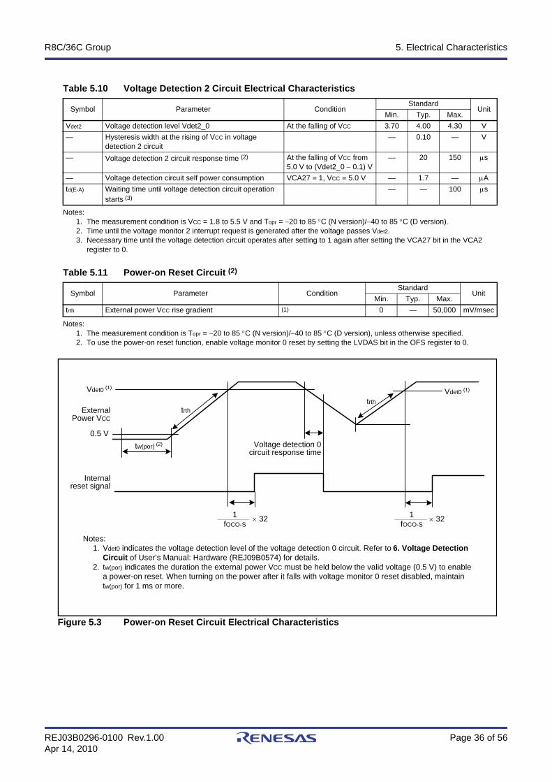
Table 5.11 Power-on Reset Circuit (2)
Symbol Parameter ConditionStandard
UnitMin. Typ. Max.
trth External power VCC rise gradient (1) 0 — 50,000 mV/msec
Notes:1. Vdet0 indicates the voltage detection level of the voltage detection 0 circuit. Refer to 6. Voltage Detection
Circuit of User’s Manual: Hardware (REJ09B0574) for details.2. tw(por) indicates the duration the external power VCC must be held below the valid voltage (0.5 V) to enable
a power-on reset. When turning on the power after it falls with voltage monitor 0 reset disabled, maintaintw(por) for 1 ms or more.
Vdet0 (1)
0.5 V
Internalreset signal
tw(por) (2) Voltage detection 0circuit response time
Vdet0 (1)
ExternalPower VCC
trthtrth
1fOCO-S
× 32 1fOCO-S
× 32
R8C/36C Group 5. Electrical Characteristics
REJ03B0296-0100 Rev.1.00 Page 37 of 56Apr 14, 2010
Notes:1. VCC = 1.8 to 5.5 V and Topr = −20 to 85 °C (N version)/−40 to 85 °C (D version), unless otherwise specified.2. This enables the setting errors of bit rates such as 9600 bps and 38400 bps to be 0% when the serial interface is used in
UART mode.
Note:1. VCC = 1.8 to 5.5 V and Topr = −20 to 85 °C (N version)/−40 to 85 °C (D version), unless otherwise specified.
Notes:1. The measurement condition is VCC = 1.8 to 5.5 V and Topr = 25 °C.2. Waiting time until the internal power supply generation circuit stabilizes during power-on.
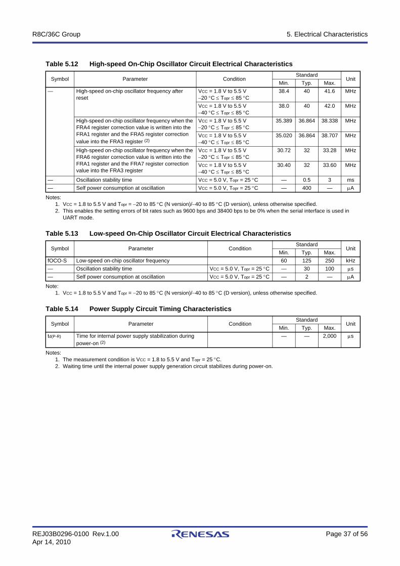
Table 5.12 High-speed On-Chip Oscillator Circuit Electrical Characteristics
Symbol Parameter ConditionStandard
UnitMin. Typ. Max.
— High-speed on-chip oscillator frequency after reset
VCC = 1.8 V to 5.5 V−20 °C ≤ Topr ≤ 85 °C
38.4 40 41.6 MHz
VCC = 1.8 V to 5.5 V−40 °C ≤ Topr ≤ 85 °C
38.0 40 42.0 MHz
High-speed on-chip oscillator frequency when the FRA4 register correction value is written into the FRA1 register and the FRA5 register correction value into the FRA3 register (2)
VCC = 1.8 V to 5.5 V−20 °C ≤ Topr ≤ 85 °C
35.389 36.864 38.338 MHz
VCC = 1.8 V to 5.5 V−40 °C ≤ Topr ≤ 85 °C
35.020 36.864 38.707 MHz
High-speed on-chip oscillator frequency when the FRA6 register correction value is written into the FRA1 register and the FRA7 register correction value into the FRA3 register
VCC = 1.8 V to 5.5 V−20 °C ≤ Topr ≤ 85 °C
30.72 32 33.28 MHz
VCC = 1.8 V to 5.5 V−40 °C ≤ Topr ≤ 85 °C
30.40 32 33.60 MHz
— Oscillation stability time VCC = 5.0 V, Topr = 25 °C — 0.5 3 ms— Self power consumption at oscillation VCC = 5.0 V, Topr = 25 °C — 400 — µA
Table 5.13 Low-speed On-Chip Oscillator Circuit Electrical Characteristics
Symbol Parameter ConditionStandard
UnitMin. Typ. Max.
fOCO-S Low-speed on-chip oscillator frequency 60 125 250 kHz— Oscillation stability time VCC = 5.0 V, Topr = 25 °C — 30 100 µs— Self power consumption at oscillation VCC = 5.0 V, Topr = 25 °C — 2 — µA
Table 5.14 Power Supply Circuit Timing Characteristics
Symbol Parameter ConditionStandard
UnitMin. Typ. Max.
td(P-R) Time for internal power supply stabilization during power-on (2)
— — 2,000 µs
R8C/36C Group 5. Electrical Characteristics
REJ03B0296-0100 Rev.1.00 Page 38 of 56Apr 14, 2010
Notes:1. VCC = 1.8 to 5.5 V, VSS = 0 V, and Topr = −20 to 85 °C (N version)/−40 to 85 °C (D version), unless otherwise specified.2. 1tCYC = 1/f1(s)
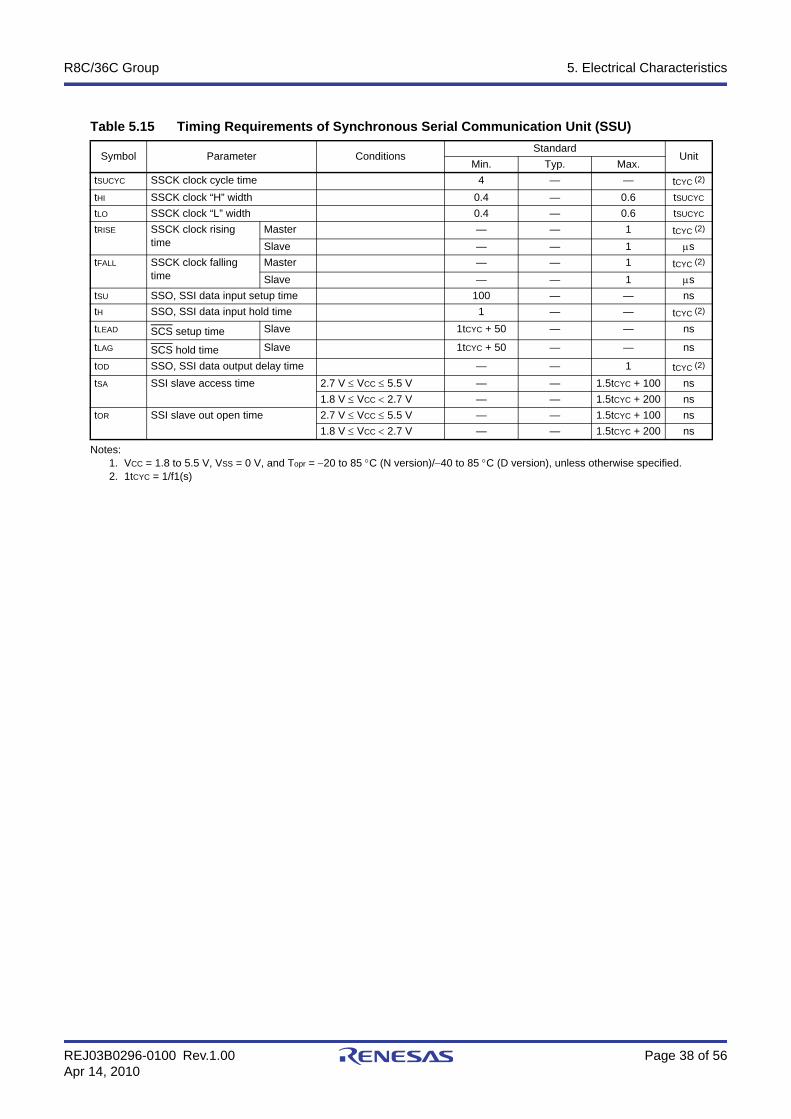
Table 5.15 Timing Requirements of Synchronous Serial Communication Unit (SSU)
Symbol Parameter ConditionsStandard
UnitMin. Typ. Max.
tSUCYC SSCK clock cycle time 4 — — tCYC (2)
tHI SSCK clock “H” width 0.4 — 0.6 tSUCYC
tLO SSCK clock “L” width 0.4 — 0.6 tSUCYC
tRISE SSCK clock rising time
Master — — 1 tCYC (2)
Slave — — 1 µstFALL SSCK clock falling
time Master — — 1 tCYC (2)
Slave — — 1 µstSU SSO, SSI data input setup time 100 — — nstH SSO, SSI data input hold time 1 — — tCYC (2)
tLEAD SCS setup time Slave 1tCYC + 50 — — ns
tLAG SCS hold time Slave 1tCYC + 50 — — ns
tOD SSO, SSI data output delay time — — 1 tCYC (2)
tSA SSI slave access time 2.7 V ≤ VCC ≤ 5.5 V — — 1.5tCYC + 100 ns1.8 V ≤ VCC < 2.7 V — — 1.5tCYC + 200 ns
tOR SSI slave out open time 2.7 V ≤ VCC ≤ 5.5 V — — 1.5tCYC + 100 ns1.8 V ≤ VCC < 2.7 V — — 1.5tCYC + 200 ns
R8C/36C Group 5. Electrical Characteristics
REJ03B0296-0100 Rev.1.00 Page 39 of 56Apr 14, 2010
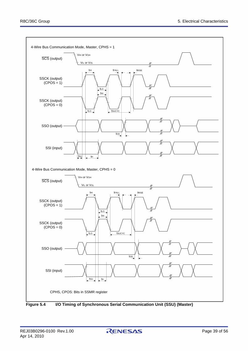
Figure 5.4 I/O Timing of Synchronous Serial Communication Unit (SSU) (Master)
VIH or VOH
VIL or VOL
tHI
tLO
tHI
tFALL tRISE
tLO tSUCYC
tOD
tHtSU
SCS (output)
SSCK (output)(CPOS = 1)
SSCK (output)(CPOS = 0)
SSO (output)
SSI (input)
4-Wire Bus Communication Mode, Master, CPHS = 1
VIH or VOH
VIL or VOL
tHI
tLO
tHI
tFALL tRISE
tLO tSUCYC
tOD
tHtSU
SCS (output)
SSCK (output)(CPOS = 1)
SSCK (output)(CPOS = 0)
SSO (output)
SSI (input)
4-Wire Bus Communication Mode, Master, CPHS = 0
CPHS, CPOS: Bits in SSMR register
R8C/36C Group 5. Electrical Characteristics
REJ03B0296-0100 Rev.1.00 Page 40 of 56Apr 14, 2010
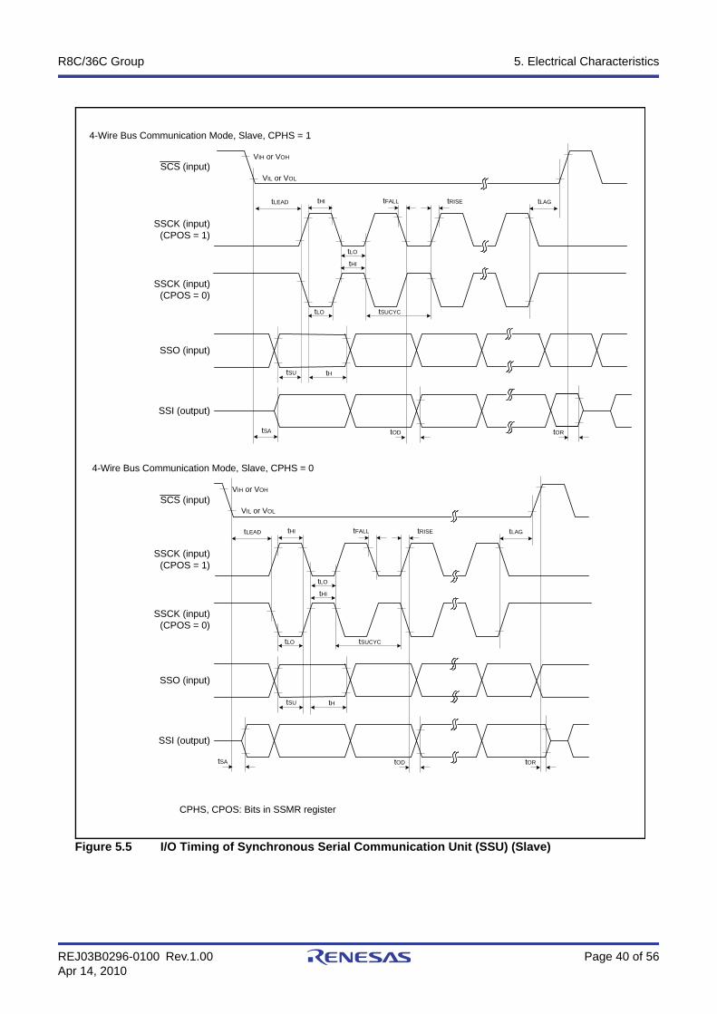
Figure 5.5 I/O Timing of Synchronous Serial Communication Unit (SSU) (Slave)
VIH or VOH
VIL or VOL
SCS (input)
SSCK (input)(CPOS = 1)
SSCK (input)(CPOS = 0)
SSO (input)
SSI (output)
4-Wire Bus Communication Mode, Slave, CPHS = 1
VIH or VOH
VIL or VOL
tHI
tLO
tHI
tFALL tRISE
tLO tSUCYC
tHtSU
SCS (input)
SSCK (input)(CPOS = 1)
SSCK (input)(CPOS = 0)
SSO (input)
SSI (output)
4-Wire Bus Communication Mode, Slave, CPHS = 0
tOD
tLEAD
tSA
tLAG
tOR
tHI
tLO
tHI
tFALL tRISE
tLO tSUCYC
tHtSU
tOD
tLEAD
tSA
tLAG
tOR
CPHS, CPOS: Bits in SSMR register
R8C/36C Group 5. Electrical Characteristics
REJ03B0296-0100 Rev.1.00 Page 41 of 56Apr 14, 2010
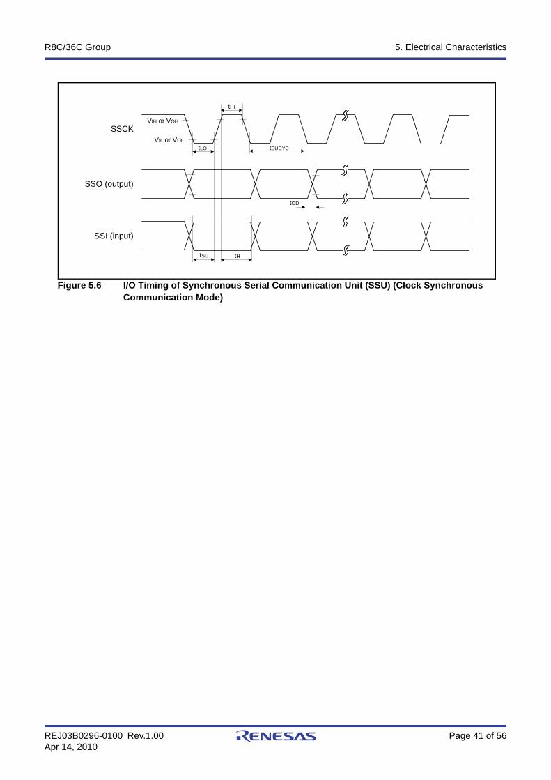
Figure 5.6 I/O Timing of Synchronous Serial Communication Unit (SSU) (Clock Synchronous Communication Mode)
VIH or VOH
tHI
tLO tSUCYC
tOD
tHtSU
SSCK
SSO (output)
SSI (input)
VIL or VOL
R8C/36C Group 5. Electrical Characteristics
REJ03B0296-0100 Rev.1.00 Page 42 of 56Apr 14, 2010
Notes:1. VCC = 1.8 to 5.5 V, VSS = 0 V, and Topr = −20 to 85 °C (N version)/−40 to 85 °C (D version), unless otherwise specified.2. 1tCYC = 1/f1(s)
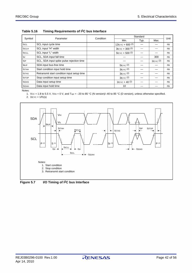
Figure 5.7 I/O Timing of I2C bus Interface
Table 5.16 Timing Requirements of I2C bus Interface
Symbol Parameter ConditionStandard
UnitMin. Typ. Max.
tSCL SCL input cycle time 12tCYC + 600 (2) — — nstSCLH SCL input “H” width 3tCYC + 300 (2) — — nstSCLL SCL input “L” width 5tCYC + 500 (2) — — nstsf SCL, SDA input fall time — — 300 nstSP SCL, SDA input spike pulse rejection time — — 1tCYC (2) nstBUF SDA input bus-free time 5tCYC (2) — — nstSTAH Start condition input hold time 3tCYC (2) — — nstSTAS Retransmit start condition input setup time 3tCYC (2) — — nstSTOP Stop condition input setup time 3tCYC (2) — — nstSDAS Data input setup time 1tCYC + 40 (2) — — nstSDAH Data input hold time 10 — — ns
SDA
SCL
Notes:1. Start condition2. Stop condition3. Retransmit start condition
tBUF
VIH
VIL
P (2) S (1)
tSTAH tSCLH
tSCLLtSf tSr
tSCL tSDAH
Sr (3) P (2)
tSDAS
tSTAStSP tSTOP
R8C/36C Group 5. Electrical Characteristics
REJ03B0296-0100 Rev.1.00 Page 43 of 56Apr 14, 2010
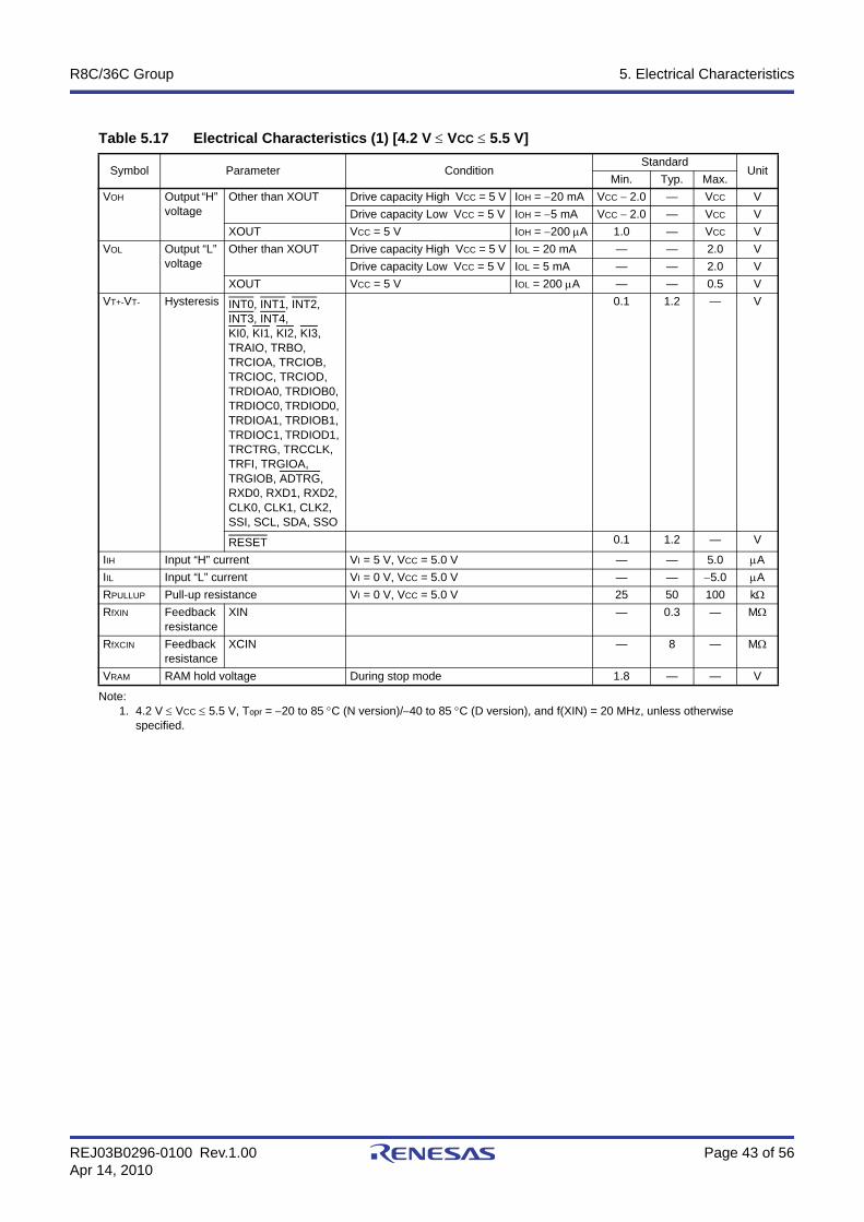
Note:1. 4.2 V ≤ VCC ≤ 5.5 V, Topr = −20 to 85 °C (N version)/−40 to 85 °C (D version), and f(XIN) = 20 MHz, unless otherwise
specified.
Table 5.17 Electrical Characteristics (1) [4.2 V ≤ VCC ≤ 5.5 V]
Symbol Parameter ConditionStandard
UnitMin. Typ. Max.
VOH Output “H” voltage
Other than XOUT Drive capacity High VCC = 5 V IOH = −20 mA VCC − 2.0 — VCC VDrive capacity Low VCC = 5 V IOH = −5 mA VCC − 2.0 — VCC V
XOUT VCC = 5 V IOH = −200 µA 1.0 — VCC VVOL Output “L”
voltageOther than XOUT Drive capacity High VCC = 5 V IOL = 20 mA — — 2.0 V
Drive capacity Low VCC = 5 V IOL = 5 mA — — 2.0 VXOUT VCC = 5 V IOL = 200 µA — — 0.5 V
VT+-VT- Hysteresis INT0, INT1, INT2, INT3, INT4, KI0, KI1, KI2, KI3, TRAIO, TRBO, TRCIOA, TRCIOB, TRCIOC, TRCIOD, TRDIOA0, TRDIOB0, TRDIOC0, TRDIOD0, TRDIOA1, TRDIOB1, TRDIOC1, TRDIOD1, TRCTRG, TRCCLK, TRFI, TRGIOA, TRGIOB, ADTRG, RXD0, RXD1, RXD2, CLK0, CLK1, CLK2, SSI, SCL, SDA, SSO
0.1 1.2 — V
RESET 0.1 1.2 — V
IIH Input “H” current VI = 5 V, VCC = 5.0 V — — 5.0 µAIIL Input “L” current VI = 0 V, VCC = 5.0 V — — −5.0 µARPULLUP Pull-up resistance VI = 0 V, VCC = 5.0 V 25 50 100 kΩRfXIN Feedback
resistanceXIN — 0.3 — MΩ
RfXCIN Feedback resistance
XCIN — 8 — MΩ
VRAM RAM hold voltage During stop mode 1.8 — — V
R8C/36C Group 5. Electrical Characteristics
REJ03B0296-0100 Rev.1.00 Page 44 of 56Apr 14, 2010
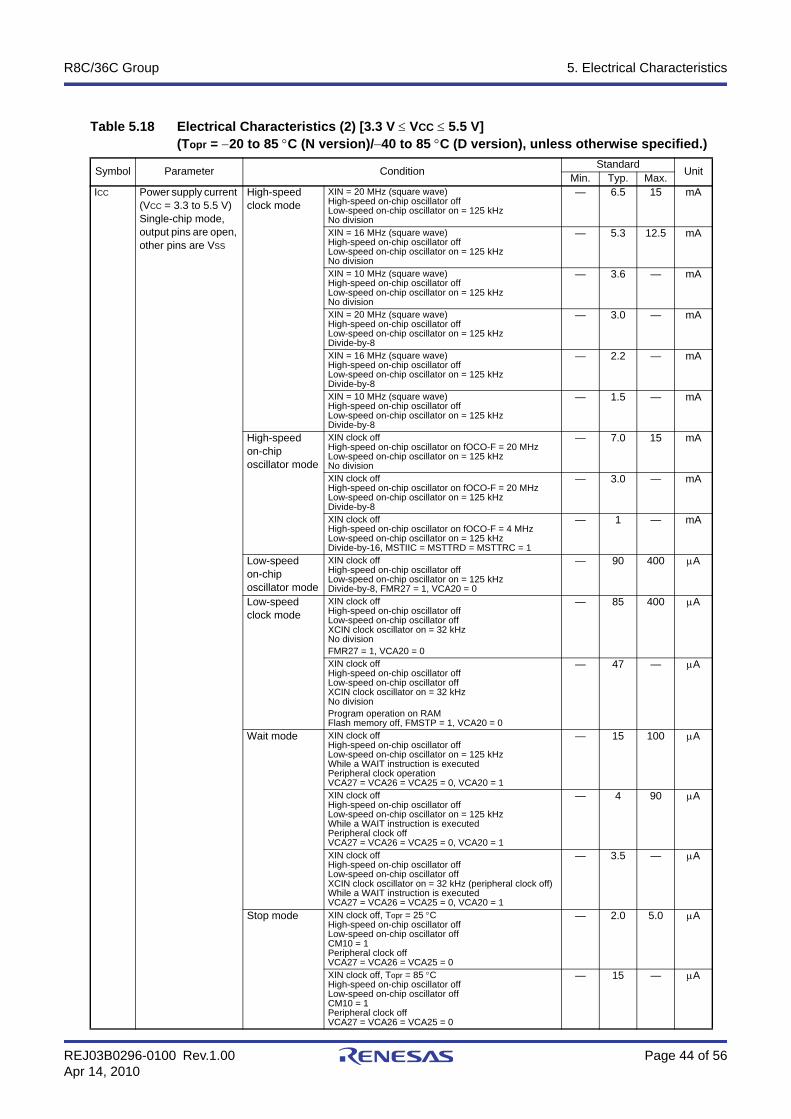
Table 5.18 Electrical Characteristics (2) [3.3 V ≤ VCC ≤ 5.5 V](Topr = −20 to 85 °C (N version)/−40 to 85 °C (D version), unless otherwise specified.)
Symbol Parameter Condition Standard UnitMin. Typ. Max.ICC Power supply current
(VCC = 3.3 to 5.5 V)Single-chip mode, output pins are open, other pins are VSS
High-speed clock mode
XIN = 20 MHz (square wave)High-speed on-chip oscillator offLow-speed on-chip oscillator on = 125 kHzNo division
— 6.5 15 mA
XIN = 16 MHz (square wave)High-speed on-chip oscillator offLow-speed on-chip oscillator on = 125 kHzNo division
— 5.3 12.5 mA
XIN = 10 MHz (square wave)High-speed on-chip oscillator offLow-speed on-chip oscillator on = 125 kHzNo division
— 3.6 — mA
XIN = 20 MHz (square wave)High-speed on-chip oscillator offLow-speed on-chip oscillator on = 125 kHzDivide-by-8
— 3.0 — mA
XIN = 16 MHz (square wave)High-speed on-chip oscillator offLow-speed on-chip oscillator on = 125 kHzDivide-by-8
— 2.2 — mA
XIN = 10 MHz (square wave)High-speed on-chip oscillator offLow-speed on-chip oscillator on = 125 kHzDivide-by-8
— 1.5 — mA
High-speed on-chip oscillator mode
XIN clock offHigh-speed on-chip oscillator on fOCO-F = 20 MHzLow-speed on-chip oscillator on = 125 kHzNo division
— 7.0 15 mA
XIN clock offHigh-speed on-chip oscillator on fOCO-F = 20 MHzLow-speed on-chip oscillator on = 125 kHzDivide-by-8
— 3.0 — mA
XIN clock offHigh-speed on-chip oscillator on fOCO-F = 4 MHzLow-speed on-chip oscillator on = 125 kHzDivide-by-16, MSTIIC = MSTTRD = MSTTRC = 1
— 1 — mA
Low-speed on-chip oscillator mode
XIN clock offHigh-speed on-chip oscillator offLow-speed on-chip oscillator on = 125 kHzDivide-by-8, FMR27 = 1, VCA20 = 0
— 90 400 µA
Low-speed clock mode
XIN clock offHigh-speed on-chip oscillator offLow-speed on-chip oscillator offXCIN clock oscillator on = 32 kHzNo divisionFMR27 = 1, VCA20 = 0
— 85 400 µA
XIN clock offHigh-speed on-chip oscillator offLow-speed on-chip oscillator offXCIN clock oscillator on = 32 kHzNo divisionProgram operation on RAMFlash memory off, FMSTP = 1, VCA20 = 0
— 47 — µA
Wait mode XIN clock offHigh-speed on-chip oscillator offLow-speed on-chip oscillator on = 125 kHzWhile a WAIT instruction is executedPeripheral clock operationVCA27 = VCA26 = VCA25 = 0, VCA20 = 1
— 15 100 µA
XIN clock offHigh-speed on-chip oscillator offLow-speed on-chip oscillator on = 125 kHzWhile a WAIT instruction is executedPeripheral clock offVCA27 = VCA26 = VCA25 = 0, VCA20 = 1
— 4 90 µA
XIN clock offHigh-speed on-chip oscillator offLow-speed on-chip oscillator offXCIN clock oscillator on = 32 kHz (peripheral clock off)While a WAIT instruction is executedVCA27 = VCA26 = VCA25 = 0, VCA20 = 1
— 3.5 — µA
Stop mode XIN clock off, Topr = 25 °CHigh-speed on-chip oscillator offLow-speed on-chip oscillator offCM10 = 1Peripheral clock offVCA27 = VCA26 = VCA25 = 0
— 2.0 5.0 µA
XIN clock off, Topr = 85 °CHigh-speed on-chip oscillator offLow-speed on-chip oscillator offCM10 = 1Peripheral clock offVCA27 = VCA26 = VCA25 = 0
— 15 — µA
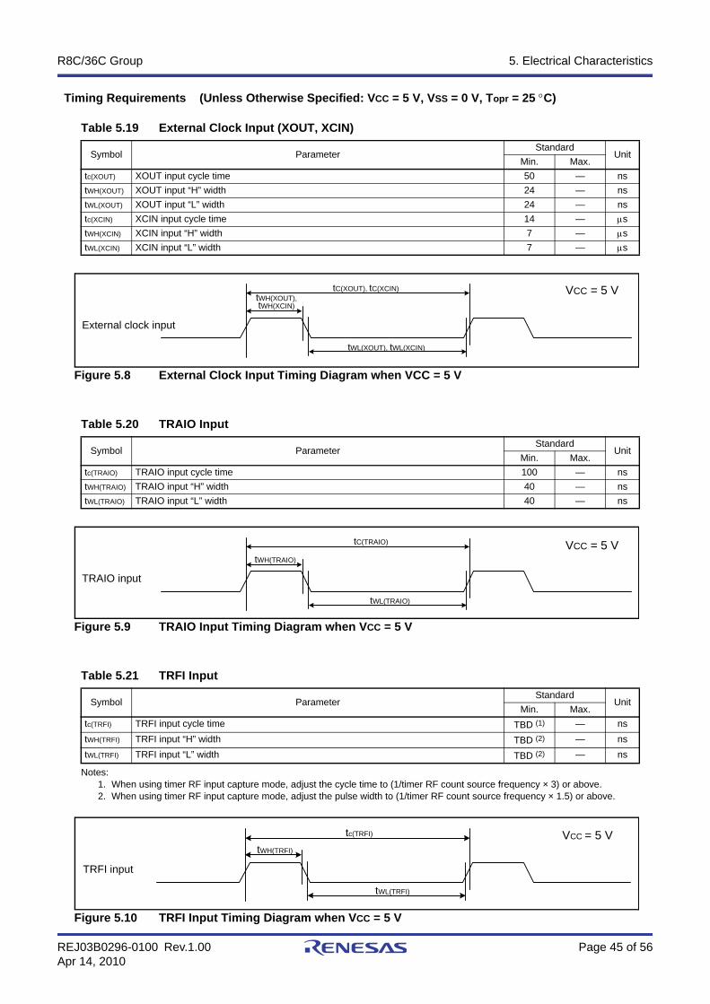
R8C/36C Group 5. Electrical Characteristics
REJ03B0296-0100 Rev.1.00 Page 45 of 56Apr 14, 2010
Timing Requirements (Unless Otherwise Specified: VCC = 5 V, VSS = 0 V, Topr = 25 °C)
Figure 5.8 External Clock Input Timing Diagram when VCC = 5 V
Figure 5.9 TRAIO Input Timing Diagram when VCC = 5 V
Notes:1. When using timer RF input capture mode, adjust the cycle time to (1/timer RF count source frequency × 3) or above.2. When using timer RF input capture mode, adjust the pulse width to (1/timer RF count source frequency × 1.5) or above.
Figure 5.10 TRFI Input Timing Diagram when VCC = 5 V
Table 5.19 External Clock Input (XOUT, XCIN)
Symbol ParameterStandard
UnitMin. Max.
tc(XOUT) XOUT input cycle time 50 — nstWH(XOUT) XOUT input “H” width 24 — nstWL(XOUT) XOUT input “L” width 24 — nstc(XCIN) XCIN input cycle time 14 — µstWH(XCIN) XCIN input “H” width 7 — µstWL(XCIN) XCIN input “L” width 7 — µs
Table 5.20 TRAIO Input
Symbol ParameterStandard
UnitMin. Max.
tc(TRAIO) TRAIO input cycle time 100 — nstWH(TRAIO) TRAIO input “H” width 40 — nstWL(TRAIO) TRAIO input “L” width 40 — ns
Table 5.21 TRFI Input
Symbol ParameterStandard
UnitMin. Max.
tc(TRFI) TRFI input cycle time TBD (1) — nstWH(TRFI) TRFI input “H” width TBD (2) — nstWL(TRFI) TRFI input “L” width TBD (2) — ns
External clock input
tWH(XOUT),tWH(XCIN)
tC(XOUT), tC(XCIN)
tWL(XOUT), tWL(XCIN)
VCC = 5 V
TRAIO input
VCC = 5 VtC(TRAIO)
tWL(TRAIO)
tWH(TRAIO)
tWH(TRFI)
tc(TRFI)
tWL(TRFI)
TRFI input
VCC = 5 V
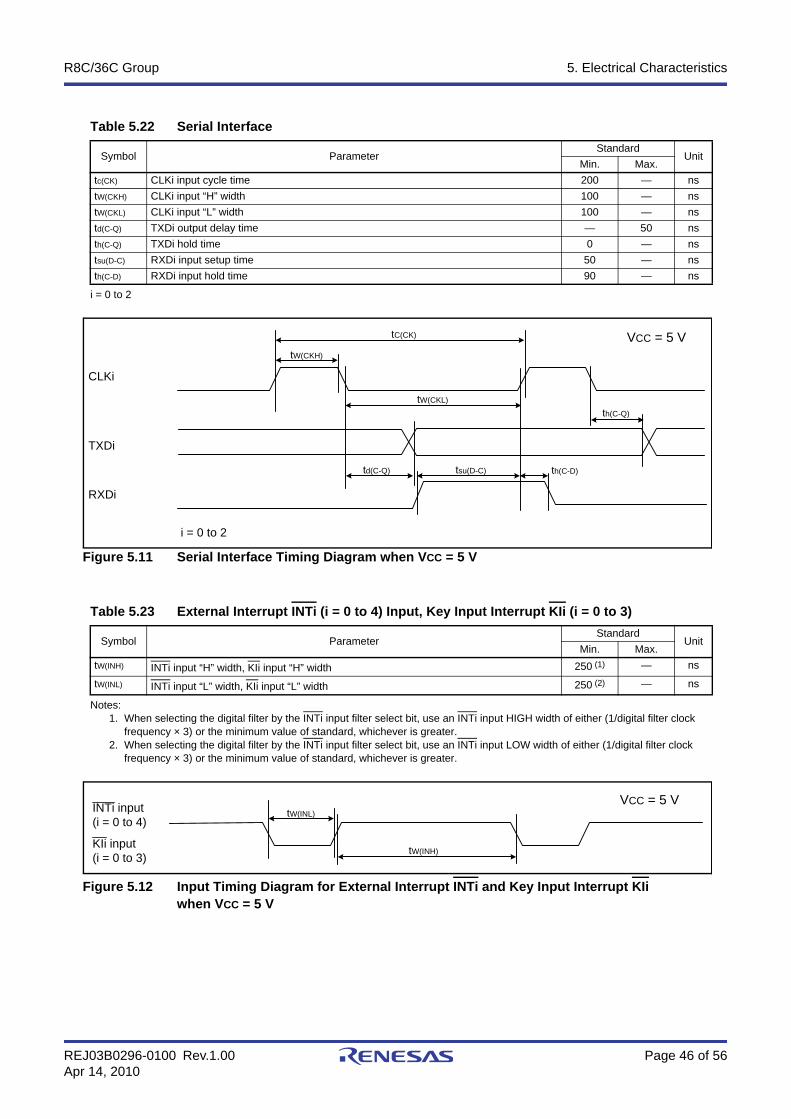
R8C/36C Group 5. Electrical Characteristics
REJ03B0296-0100 Rev.1.00 Page 46 of 56Apr 14, 2010
i = 0 to 2
Figure 5.11 Serial Interface Timing Diagram when VCC = 5 V
Notes:1. When selecting the digital filter by the INTi input filter select bit, use an INTi input HIGH width of either (1/digital filter clock
frequency × 3) or the minimum value of standard, whichever is greater.2. When selecting the digital filter by the INTi input filter select bit, use an INTi input LOW width of either (1/digital filter clock
frequency × 3) or the minimum value of standard, whichever is greater.
Figure 5.12 Input Timing Diagram for External Interrupt INTi and Key Input Interrupt KIi when VCC = 5 V
Table 5.22 Serial Interface
Symbol ParameterStandard
UnitMin. Max.
tc(CK) CLKi input cycle time 200 — nstW(CKH) CLKi input “H” width 100 — nstW(CKL) CLKi input “L” width 100 — nstd(C-Q) TXDi output delay time — 50 nsth(C-Q) TXDi hold time 0 — nstsu(D-C) RXDi input setup time 50 — nsth(C-D) RXDi input hold time 90 — ns
Table 5.23 External Interrupt INTi (i = 0 to 4) Input, Key Input Interrupt KIi (i = 0 to 3)
Symbol ParameterStandard
UnitMin. Max.
tW(INH) INTi input “H” width, KIi input “H” width 250 (1) — ns
tW(INL) INTi input “L” width, KIi input “L” width 250 (2) — ns
tW(CKH)
tC(CK)
tW(CKL)
th(C-Q)
th(C-D)tsu(D-C)td(C-Q)
CLKi
TXDi
RXDi
i = 0 to 2
VCC = 5 V
INTi input(i = 0 to 4)
tW(INL)
tW(INH)
VCC = 5 V
KIi input(i = 0 to 3)
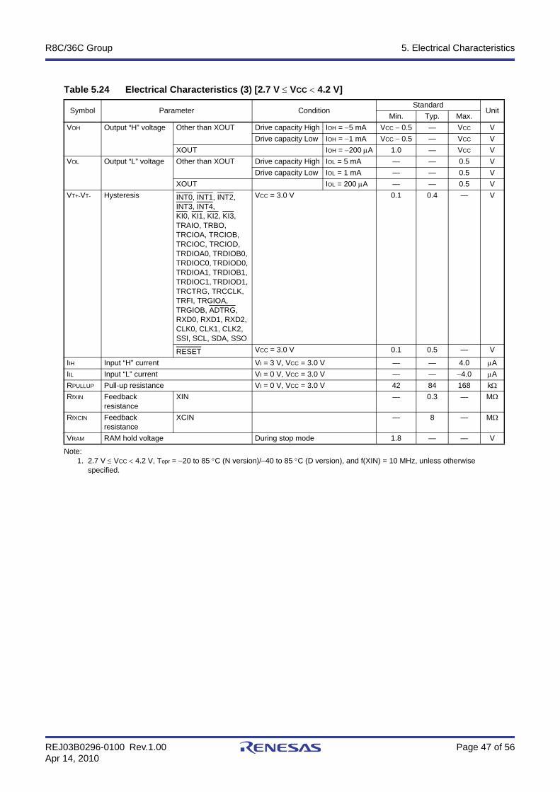
R8C/36C Group 5. Electrical Characteristics
REJ03B0296-0100 Rev.1.00 Page 47 of 56Apr 14, 2010
Note:1. 2.7 V ≤ VCC < 4.2 V, Topr = −20 to 85 °C (N version)/−40 to 85 °C (D version), and f(XIN) = 10 MHz, unless otherwise
specified.
Table 5.24 Electrical Characteristics (3) [2.7 V ≤ VCC < 4.2 V]
Symbol Parameter ConditionStandard
UnitMin. Typ. Max.
VOH Output “H” voltage Other than XOUT Drive capacity High IOH = −5 mA VCC − 0.5 — VCC VDrive capacity Low IOH = −1 mA VCC − 0.5 — VCC V
XOUT IOH = −200 µA 1.0 — VCC VVOL Output “L” voltage Other than XOUT Drive capacity High IOL = 5 mA — — 0.5 V
Drive capacity Low IOL = 1 mA — — 0.5 VXOUT IOL = 200 µA — — 0.5 V
VT+-VT- Hysteresis INT0, INT1, INT2, INT3, INT4, KI0, KI1, KI2, KI3, TRAIO, TRBO, TRCIOA, TRCIOB, TRCIOC, TRCIOD, TRDIOA0, TRDIOB0, TRDIOC0, TRDIOD0, TRDIOA1, TRDIOB1, TRDIOC1, TRDIOD1, TRCTRG, TRCCLK, TRFI, TRGIOA, TRGIOB, ADTRG, RXD0, RXD1, RXD2, CLK0, CLK1, CLK2, SSI, SCL, SDA, SSO
VCC = 3.0 V 0.1 0.4 — V
RESET VCC = 3.0 V 0.1 0.5 — V
IIH Input “H” current VI = 3 V, VCC = 3.0 V — — 4.0 µAIIL Input “L” current VI = 0 V, VCC = 3.0 V — — −4.0 µARPULLUP Pull-up resistance VI = 0 V, VCC = 3.0 V 42 84 168 kΩRfXIN Feedback
resistanceXIN — 0.3 — MΩ
RfXCIN Feedback resistance
XCIN — 8 — MΩ
VRAM RAM hold voltage During stop mode 1.8 — — V
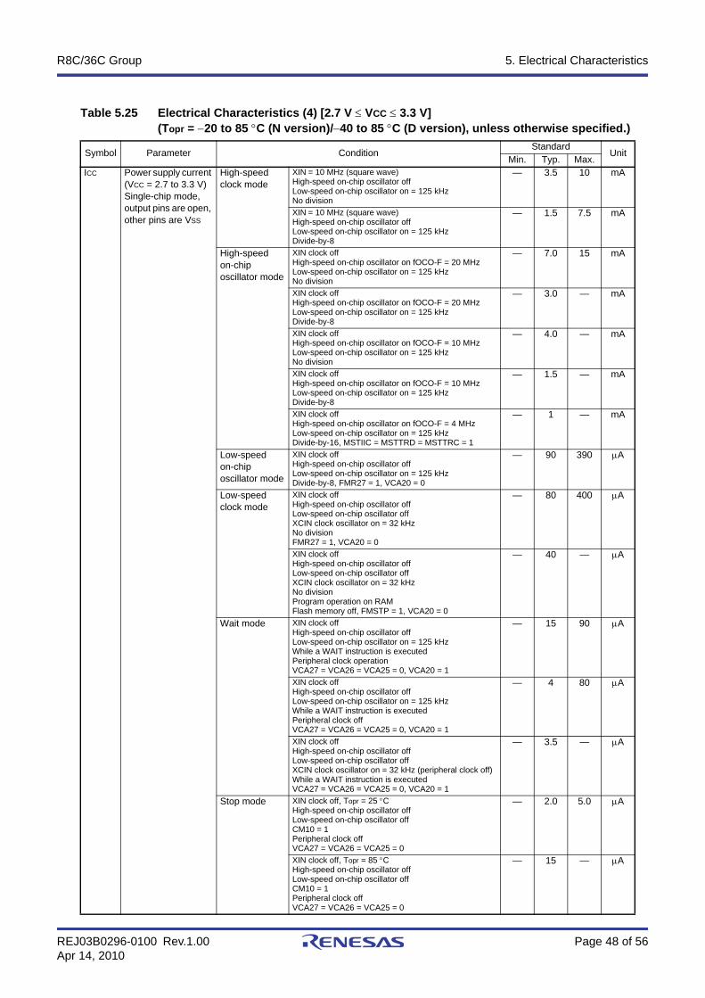
R8C/36C Group 5. Electrical Characteristics
REJ03B0296-0100 Rev.1.00 Page 48 of 56Apr 14, 2010
Table 5.25 Electrical Characteristics (4) [2.7 V ≤ VCC ≤ 3.3 V](Topr = −20 to 85 °C (N version)/−40 to 85 °C (D version), unless otherwise specified.)
Symbol Parameter ConditionStandard
UnitMin. Typ. Max.
ICC Power supply current (VCC = 2.7 to 3.3 V)Single-chip mode, output pins are open, other pins are VSS
High-speed clock mode
XIN = 10 MHz (square wave)High-speed on-chip oscillator offLow-speed on-chip oscillator on = 125 kHzNo division
— 3.5 10 mA
XIN = 10 MHz (square wave)High-speed on-chip oscillator offLow-speed on-chip oscillator on = 125 kHzDivide-by-8
— 1.5 7.5 mA
High-speed on-chip oscillator mode
XIN clock offHigh-speed on-chip oscillator on fOCO-F = 20 MHzLow-speed on-chip oscillator on = 125 kHzNo division
— 7.0 15 mA
XIN clock offHigh-speed on-chip oscillator on fOCO-F = 20 MHzLow-speed on-chip oscillator on = 125 kHzDivide-by-8
— 3.0 — mA
XIN clock offHigh-speed on-chip oscillator on fOCO-F = 10 MHzLow-speed on-chip oscillator on = 125 kHzNo division
— 4.0 — mA
XIN clock offHigh-speed on-chip oscillator on fOCO-F = 10 MHzLow-speed on-chip oscillator on = 125 kHzDivide-by-8
— 1.5 — mA
XIN clock offHigh-speed on-chip oscillator on fOCO-F = 4 MHzLow-speed on-chip oscillator on = 125 kHzDivide-by-16, MSTIIC = MSTTRD = MSTTRC = 1
— 1 — mA
Low-speed on-chip oscillator mode
XIN clock offHigh-speed on-chip oscillator offLow-speed on-chip oscillator on = 125 kHzDivide-by-8, FMR27 = 1, VCA20 = 0
— 90 390 µA
Low-speed clock mode
XIN clock offHigh-speed on-chip oscillator offLow-speed on-chip oscillator offXCIN clock oscillator on = 32 kHz No divisionFMR27 = 1, VCA20 = 0
— 80 400 µA
XIN clock offHigh-speed on-chip oscillator offLow-speed on-chip oscillator offXCIN clock oscillator on = 32 kHz No divisionProgram operation on RAMFlash memory off, FMSTP = 1, VCA20 = 0
— 40 — µA
Wait mode XIN clock offHigh-speed on-chip oscillator offLow-speed on-chip oscillator on = 125 kHzWhile a WAIT instruction is executedPeripheral clock operationVCA27 = VCA26 = VCA25 = 0, VCA20 = 1
— 15 90 µA
XIN clock offHigh-speed on-chip oscillator offLow-speed on-chip oscillator on = 125 kHzWhile a WAIT instruction is executedPeripheral clock offVCA27 = VCA26 = VCA25 = 0, VCA20 = 1
— 4 80 µA
XIN clock offHigh-speed on-chip oscillator offLow-speed on-chip oscillator offXCIN clock oscillator on = 32 kHz (peripheral clock off)While a WAIT instruction is executedVCA27 = VCA26 = VCA25 = 0, VCA20 = 1
— 3.5 — µA
Stop mode XIN clock off, Topr = 25 °CHigh-speed on-chip oscillator offLow-speed on-chip oscillator offCM10 = 1Peripheral clock offVCA27 = VCA26 = VCA25 = 0
— 2.0 5.0 µA
XIN clock off, Topr = 85 °CHigh-speed on-chip oscillator offLow-speed on-chip oscillator offCM10 = 1Peripheral clock offVCA27 = VCA26 = VCA25 = 0
— 15 — µA
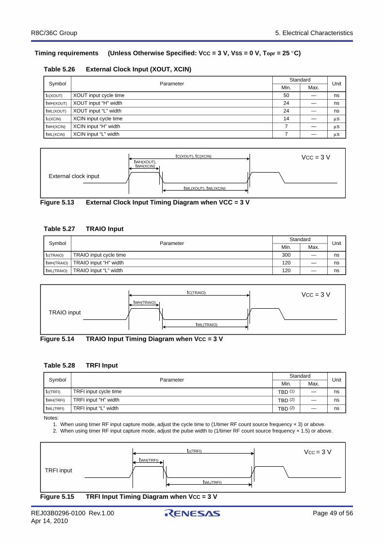
R8C/36C Group 5. Electrical Characteristics
REJ03B0296-0100 Rev.1.00 Page 49 of 56Apr 14, 2010
Timing requirements (Unless Otherwise Specified: VCC = 3 V, VSS = 0 V, Topr = 25 °C)
Figure 5.13 External Clock Input Timing Diagram when VCC = 3 V
Figure 5.14 TRAIO Input Timing Diagram when VCC = 3 V
Notes:1. When using timer RF input capture mode, adjust the cycle time to (1/timer RF count source frequency × 3) or above.2. When using timer RF input capture mode, adjust the pulse width to (1/timer RF count source frequency × 1.5) or above.
Figure 5.15 TRFI Input Timing Diagram when VCC = 3 V
Table 5.26 External Clock Input (XOUT, XCIN)
Symbol ParameterStandard
UnitMin. Max.
tc(XOUT) XOUT input cycle time 50 — nstWH(XOUT) XOUT input “H” width 24 — nstWL(XOUT) XOUT input “L” width 24 — nstc(XCIN) XCIN input cycle time 14 — µstWH(XCIN) XCIN input “H” width 7 — µstWL(XCIN) XCIN input “L” width 7 — µs
Table 5.27 TRAIO Input
Symbol ParameterStandard
UnitMin. Max.
tc(TRAIO) TRAIO input cycle time 300 — nstWH(TRAIO) TRAIO input “H” width 120 — nstWL(TRAIO) TRAIO input “L” width 120 — ns
Table 5.28 TRFI Input
Symbol ParameterStandard
UnitMin. Max.
tc(TRFI) TRFI input cycle time TBD (1) — nstWH(TRFI) TRFI input “H” width TBD (2) — nstWL(TRFI) TRFI input “L” width TBD (2) — ns
External clock input
tWH(XOUT),tWH(XCIN)
tC(XOUT), tC(XCIN)
tWL(XOUT), tWL(XCIN)
VCC = 3 V
TRAIO input
VCC = 3 VtC(TRAIO)
tWL(TRAIO)
tWH(TRAIO)
tWH(TRFI)
tc(TRFI)
tWL(TRFI)
TRFI input
VCC = 3 V
R8C/36C Group 5. Electrical Characteristics
REJ03B0296-0100 Rev.1.00 Page 50 of 56Apr 14, 2010
i = 0 to 2
Figure 5.16 Serial Interface Timing Diagram when VCC = 3 V
Notes:1. When selecting the digital filter by the INTi input filter select bit, use an INTi input HIGH width of either (1/digital filter clock
frequency × 3) or the minimum value of standard, whichever is greater.2. When selecting the digital filter by the INTi input filter select bit, use an INTi input LOW width of either (1/digital filter clock
frequency × 3) or the minimum value of standard, whichever is greater.
Figure 5.17 Input Timing Diagram for External Interrupt INTi and Key Input Interrupt KIi when VCC = 3 V
Table 5.29 Serial Interface
Symbol ParameterStandard
UnitMin. Max.
tc(CK) CLKi input cycle time 300 — nstW(CKH) CLKi input “H” width 150 — nstW(CKL) CLKi Input “L” width 150 — nstd(C-Q) TXDi output delay time — 80 nsth(C-Q) TXDi hold time 0 — nstsu(D-C) RXDi input setup time 70 — nsth(C-D) RXDi input hold time 90 — ns
Table 5.30 External Interrupt INTi (i = 0 to 4) Input, Key Input Interrupt KIi (i = 0 to 3)
Symbol ParameterStandard
UnitMin. Max.
tW(INH) INTi input “H” width, KIi input “H” width 380 (1) — ns
tW(INL) INTi input “L” width, KIi input “L” width 380 (2) — ns
tW(CKH)
tC(CK)
tW(CKL)
th(C-Q)
th(C-D)tsu(D-C)td(C-Q)
CLKi
TXDi
RXDi
VCC = 3 V
i = 0 to 2
tW(INL)
tW(INH)
VCC = 3 VINTi input(i = 0 to 4)
KIi input(i = 0 to 3)

R8C/36C Group 5. Electrical Characteristics
REJ03B0296-0100 Rev.1.00 Page 51 of 56Apr 14, 2010
Note:1. 1.8 V ≤ VCC < 2.7 V, Topr = −20 to 85 °C (N version)/−40 to 85 °C (D version), and f(XIN) = 5 MHz, unless otherwise specified.
Table 5.31 Electrical Characteristics (5) [1.8 V ≤ VCC < 2.7 V]
Symbol Parameter ConditionStandard
UnitMin. Typ. Max.
VOH Output “H” voltage Other than XOUT Drive capacity High IOH = −2 mA VCC − 0.5 — VCC VDrive capacity Low IOH = −1 mA VCC − 0.5 — VCC V
XOUT IOH = −200 µA 1.0 — VCC VVOL Output “L” voltage Other than XOUT Drive capacity High IOL = 2 mA — — 0.5 V
Drive capacity Low IOL = 1 mA — — 0.5 VXOUT IOL = 200 µA — — 0.5 V
VT+-VT- Hysteresis NT0, INT1, INT2, INT3, INT4, KI0, KI1, KI2, KI3, TRAIO, TRBO, TRCIOA, TRCIOB, TRCIOC, TRCIOD, TRDIOA0, TRDIOB0, TRDIOC0, TRDIOD0, TRDIOA1, TRDIOB1, TRDIOC1, TRDIOD1, TRCTRG, TRCCLK, TRFI, TRGIOA, TRGIOB, ADTRG, RXD0, RXD1, RXD2, CLK0, CLK1, CLK2, SSI, SCL, SDA, SSO
0.05 0.20 — V
RESET 0.05 0.20 — V
IIH Input “H” current VI = 2.2 V, VCC = 2.2 V — — 4.0 µAIIL Input “L” current VI = 0 V, VCC = 2.2 V — — −4.0 µARPULLUP Pull-up resistance VI = 0 V, VCC = 2.2 V 70 140 300 kΩRfXIN Feedback
resistanceXIN — 0.3 — MΩ
RfXCIN Feedback resistance
XCIN — 8 — MΩ
VRAM RAM hold voltage During stop mode 1.8 — — V
R8C/36C Group 5. Electrical Characteristics
REJ03B0296-0100 Rev.1.00 Page 52 of 56Apr 14, 2010
Table 5.32 Electrical Characteristics (6) [1.8 V ≤ VCC < 2.7 V](Topr = −20 to 85 °C (N version)/−40 to 85 °C (D version), unless otherwise specified.)
Symbol Parameter ConditionStandard
UnitMin. Typ. Max.
ICC Power supply current (VCC = 1.8 to 2.7 V)Single-chip mode, output pins are open, other pins are VSS
High-speed clock mode
XIN = 5 MHz (square wave)High-speed on-chip oscillator offLow-speed on-chip oscillator on = 125 kHzNo division
— 2.2 — mA
XIN = 5 MHz (square wave)High-speed on-chip oscillator offLow-speed on-chip oscillator on = 125 kHzDivide-by-8
— 0.8 — mA
High-speed on-chip oscillator mode
XIN clock offHigh-speed on-chip oscillator on fOCO-F = 5 MHzLow-speed on-chip oscillator on = 125 kHzNo division
— 2.5 10 mA
XIN clock offHigh-speed on-chip oscillator on fOCO-F = 5 MHzLow-speed on-chip oscillator on = 125 kHzDivide-by-8
— 1.7 — mA
XIN clock offHigh-speed on-chip oscillator on fOCO-F = 4 MHzLow-speed on-chip oscillator on = 125 kHzDivide-by-16, MSTIIC = MSTTRD = MSTTRC = 1
— 1 — mA
Low-speed on-chip oscillator mode
XIN clock offHigh-speed on-chip oscillator offLow-speed on-chip oscillator on = 125 kHzDivide-by-8, FMR27 = 1, VCA20 = 0
— 90 300 µA
Low-speed clock mode
XIN clock offHigh-speed on-chip oscillator offLow-speed on-chip oscillator offXCIN clock oscillator on = 32 kHz No divisionFMR27 = 1, VCA20 = 0
— 80 350 µA
XIN clock offHigh-speed on-chip oscillator offLow-speed on-chip oscillator offXCIN clock oscillator on = 32 kHz No divisionProgram operation on RAMFlash memory off, FMSTP = 1, VCA20 = 0
— 40 — µA
Wait mode XIN clock offHigh-speed on-chip oscillator offLow-speed on-chip oscillator on = 125 kHzWhile a WAIT instruction is executedPeripheral clock operationVCA27 = VCA26 = VCA25 = 0, VCA20 = 1
— 15 90 µA
XIN clock offHigh-speed on-chip oscillator offLow-speed on-chip oscillator on = 125 kHzWhile a WAIT instruction is executedPeripheral clock offVCA27 = VCA26 = VCA25 = 0, VCA20 = 1
— 4 80 µA
XIN clock offHigh-speed on-chip oscillator offLow-speed on-chip oscillator offXCIN clock oscillator on = 32 kHz (peripheral clock off)While a WAIT instruction is executedVCA27 = VCA26 = VCA25 = 0, VCA20 = 1
— 3.5 — µA
Stop mode XIN clock off, Topr = 25 °CHigh-speed on-chip oscillator offLow-speed on-chip oscillator offCM10 = 1Peripheral clock offVCA27 = VCA26 = VCA25 = 0
— 2.0 5 µA
XIN clock off, Topr = 85 °CHigh-speed on-chip oscillator offLow-speed on-chip oscillator offCM10 = 1Peripheral clock offVCA27 = VCA26 = VCA25 = 0
— 15 — µA
R8C/36C Group 5. Electrical Characteristics
REJ03B0296-0100 Rev.1.00 Page 53 of 56Apr 14, 2010
Timing requirements (Unless Otherwise Specified: VCC = 2.2 V, VSS = 0 V, Topr = 25 °C)
Figure 5.18 External Clock Input Timing Diagram when VCC = 2.2 V
Figure 5.19 TRAIO Input Timing Diagram when VCC = 2.2 V
Notes:1. When using timer RF input capture mode, adjust the cycle time to (1/timer RF count source frequency × 3) or above.2. When using timer RF input capture mode, adjust the pulse width to (1/timer RF count source frequency × 1.5) or above.
Figure 5.20 TRFI Input Timing Diagram when VCC = 2.2 V
Table 5.33 External Clock Input (XOUT, XCIN)
Symbol ParameterStandard
UnitMin. Max.
tc(XOUT) XOUT input cycle time 200 — nstWH(XOUT) XOUT input “H” width 90 — nstWL(XOUT) XOUT input “L” width 90 — nstc(XCIN) XCIN input cycle time 14 — µstWH(XCIN) XCIN input “H” width 7 — µstWL(XCIN) XCIN input “L” width 7 — µs
Table 5.34 TRAIO Input
Symbol ParameterStandard
UnitMin. Max.
tc(TRAIO) TRAIO input cycle time 500 — nstWH(TRAIO) TRAIO input “H” width 200 — nstWL(TRAIO) TRAIO input “L” width 200 — ns
Table 5.35 TRFI Input
Symbol ParameterStandard
UnitMin. Max.
tc(TRFI) TRFI input cycle time TBD (1) — nstWH(TRFI) TRFI input “H” width TBD (2) — nstWL(TRFI) TRFI input “L” width TBD (2) — ns
External clock input
tWH(XOUT),tWH(XCIN)
tC(XOUT), tC(XCIN)
tWL(XOUT), tWL(XCIN)
VCC = 2.2 V
TRAIO input
tC(TRAIO)
tWL(TRAIO)
tWH(TRAIO)
VCC = 2.2 V
tWH(TRFI)
tc(TRFI)
tWL(TRFI)
TRFI input
VCC = 2.2 V
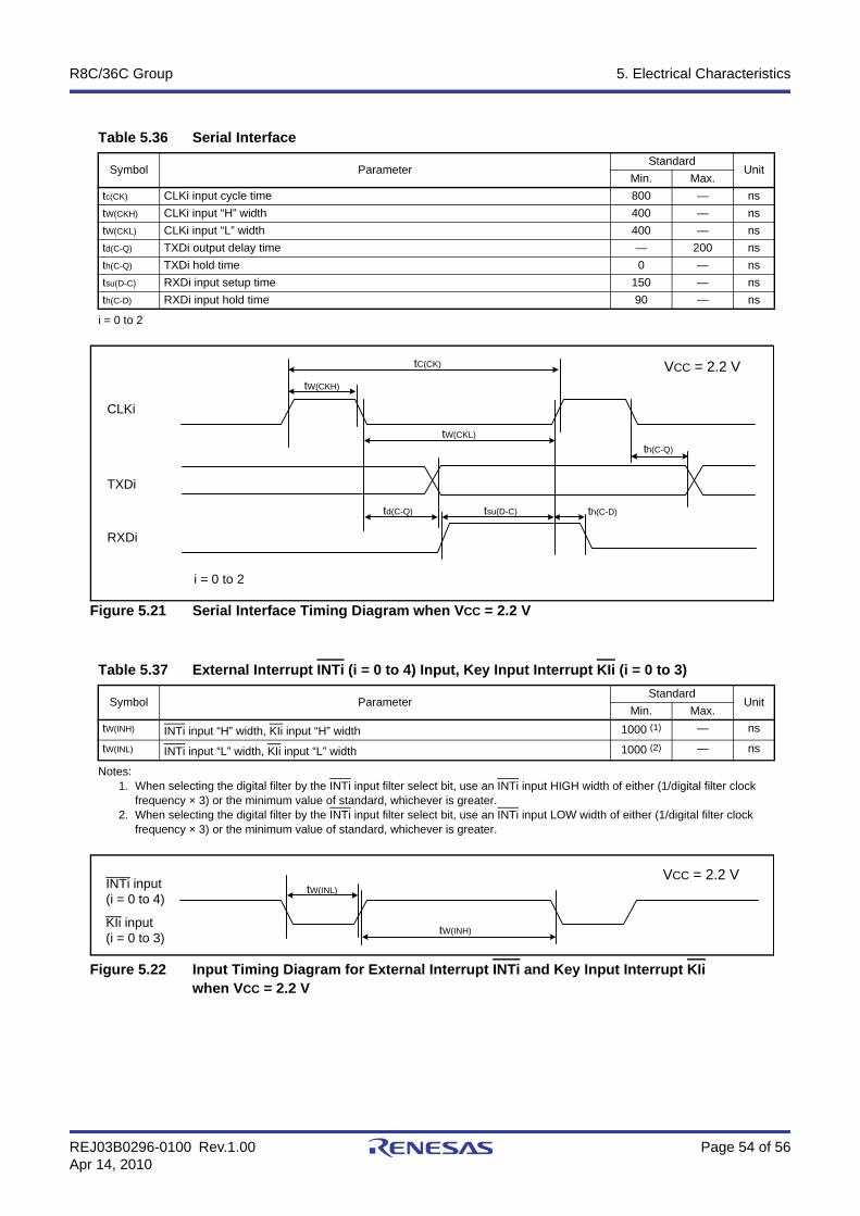
R8C/36C Group 5. Electrical Characteristics
REJ03B0296-0100 Rev.1.00 Page 54 of 56Apr 14, 2010
i = 0 to 2
Figure 5.21 Serial Interface Timing Diagram when VCC = 2.2 V
Notes:1. When selecting the digital filter by the INTi input filter select bit, use an INTi input HIGH width of either (1/digital filter clock
frequency × 3) or the minimum value of standard, whichever is greater.2. When selecting the digital filter by the INTi input filter select bit, use an INTi input LOW width of either (1/digital filter clock
frequency × 3) or the minimum value of standard, whichever is greater.
Figure 5.22 Input Timing Diagram for External Interrupt INTi and Key Input Interrupt KIi when VCC = 2.2 V
Table 5.36 Serial Interface
Symbol ParameterStandard
UnitMin. Max.
tc(CK) CLKi input cycle time 800 — nstW(CKH) CLKi input “H” width 400 — nstW(CKL) CLKi input “L” width 400 — nstd(C-Q) TXDi output delay time — 200 nsth(C-Q) TXDi hold time 0 — nstsu(D-C) RXDi input setup time 150 — nsth(C-D) RXDi input hold time 90 — ns
Table 5.37 External Interrupt INTi (i = 0 to 4) Input, Key Input Interrupt KIi (i = 0 to 3)
Symbol ParameterStandard
UnitMin. Max.
tW(INH) INTi input “H” width, KIi input “H” width 1000 (1) — ns
tW(INL) INTi input “L” width, KIi input “L” width 1000 (2) — ns
tW(CKH)
tC(CK)
tW(CKL)
th(C-Q)
th(C-D)tsu(D-C)td(C-Q)
CLKi
TXDi
RXDi
VCC = 2.2 V
i = 0 to 2
tW(INL)
tW(INH)
VCC = 2.2 VINTi input(i = 0 to 4)
KIi input(i = 0 to 3)
R8C/36C Group Package Dimensions
REJ03B0296-0100 Rev.1.00 Page 55 of 56Apr 14, 2010
Package DimensionsDiagrams showing the latest package dimensions and mounting information are available in the “Packages” section ofthe Renesas Electronics website.
Terminal cross section
b1
c 1
bp
c
2.
1. DIMENSIONS "*1" AND "*2"DO NOT INCLUDE MOLD FLASH.
NOTE)
DIMENSION "*3" DOES NOTINCLUDE TRIM OFFSET.
Index mark
*3
17
32
64
49
1 16
3348
F
*1*2
xbp
HEE
HD
D
ZD
ZE
Detail F
A cA2
A1
L1
L
P-LQFP64-10x10-0.50 0.3g
MASS[Typ.]
64P6Q-A / FP-64K / FP-64KVPLQP0064KB-A
RENESAS CodeJEITA Package Code Previous Code
1.0
0.125
0.18
1.25
1.25
0.08
0.200.1450.09
0.250.200.15
MaxNomMin
Dimension in MillimetersSymbol
Reference
10.110.09.9D
10.110.09.9E
1.4A2
12.212.011.8
12.212.011.8
1.7A
0.150.10.05
0.650.50.35L
x
8°0°
c
0.5e
0.08y
HD
HE
A1
bp
b1
c1
ZD
ZE
L1
e
y S
S
R8C/36C Group Package Dimensions
REJ03B0296-0100 Rev.1.00 Page 56 of 56Apr 14, 2010
Terminal cross section
b1
c1
bp
c
2.
1. DIMENSIONS "*1" AND "*2"DO NOT INCLUDE MOLD FLASH.
NOTE)
DIMENSION "*3" DOES NOTINCLUDE TRIM OFFSET.
*3
1 16
17
32
3348
49
64
F
*1
*2
x
Index mark
D
HD
E HE
e bp
ZD
ZE
Detail F
c
A A2
A1
L
L1
Previous CodeJEITA Package Code RENESAS Code
PLQP0064GA-A 64P6U-A/
MASS[Typ.]
0.7gP-LQFP64-14x14-0.80
1.0
0.125
0.35
1.0
1.0
0.20
0.200.1450.09
0.420.370.32
MaxNomMin
Dimension in MillimetersSymbol
Reference
14.114.013.9D
14.114.013.9E
1.4A2
16.216.015.8
16.216.015.8
1.7A
0.20.10
0.70.50.3L
x
8°0°
c
0.8e
0.10y
HD
HE
A1
bp
b1
c1
ZD
ZE
L1
y S
S
R8C/36C Group Datasheet
C - 1
Rev. DateDescription
Page Summary0.01 Oct 30, 2009 — First Edition issued1.00 Apr 14, 2010 All pages “Preliminary”, “Under development” deleted
4 Table 1.3 revised28 to 54 “5. Electrical Characteristics” added
All trademarks and registered trademarks are the property of their respective owners.
REVISION HISTORY
General Precautions in the Handling of MPU/MCU Products
The following usage notes are applicable to all MPU/MCU products from Renesas. For detailed usage notes on the products covered by this manual, refer to the relevant sections of the manual. If the descriptions under General Precautions in the Handling of MPU/MCU Products and in the body of the manual differ from each other, the description in the body of the manual takes precedence.
1. Handling of Unused Pins Handle unused pins in accord with the directions given under Handling of Unused Pins in the manual. The input pins of CMOS products are generally in the high-impedance state. In operation
with an unused pin in the open-circuit state, extra electromagnetic noise is induced in the vicinity of LSI, an associated shoot-through current flows internally, and malfunctions occur due to the false recognition of the pin state as an input signal become possible. Unused pins should be handled as described under Handling of Unused Pins in the manual.
2. Processing at Power-on The state of the product is undefined at the moment when power is supplied. The states of internal circuits in the LSI are indeterminate and the states of register
settings and pins are undefined at the moment when power is supplied. In a finished product where the reset signal is applied to the external reset pin, the states of pins are not guaranteed from the moment when power is supplied until the reset process is completed. In a similar way, the states of pins in a product that is reset by an on-chip power-on reset function are not guaranteed from the moment when power is supplied until the power reaches the level at which resetting has been specified.
3. Prohibition of Access to Reserved Addresses Access to reserved addresses is prohibited. The reserved addresses are provided for the possible future expansion of functions. Do
not access these addresses; the correct operation of LSI is not guaranteed if they are accessed.
4. Clock Signals After applying a reset, only release the reset line after the operating clock signal has become stable. When switching the clock signal during program execution, wait until the target clock signal has stabilized. When the clock signal is generated with an external resonator (or from an external
oscillator) during a reset, ensure that the reset line is only released after full stabilization of the clock signal. Moreover, when switching to a clock signal produced with an external resonator (or by an external oscillator) while program execution is in progress, wait until the target clock signal is stable.
5. Differences between Products Before changing from one product to another, i.e. to one with a different part number, confirm that the change will not lead to problems. The characteristics of MPU/MCU in the same group but having different part numbers may
differ because of the differences in internal memory capacity and layout pattern. When changing to products of different part numbers, implement a system-evaluation test for each of the products.
Notice1. All information included in this document is current as of the date this document is issued. Such information, however, is subject to change without any prior notice. Before purchasing or using any Renesas
Electronics products listed herein, please confirm the latest product information with a Renesas Electronics sales office. Also, please pay regular and careful attention to additional and different information to
be disclosed by Renesas Electronics such as that disclosed through our website.
2. Renesas Electronics does not assume any liability for infringement of patents, copyrights, or other intellectual property rights of third parties by or arising from the use of Renesas Electronics products or
technical information described in this document. No license, express, implied or otherwise, is granted hereby under any patents, copyrights or other intellectual property rights of Renesas Electronics or
others.
3. You should not alter, modify, copy, or otherwise misappropriate any Renesas Electronics product, whether in whole or in part.
4. Descriptions of circuits, software and other related information in this document are provided only to illustrate the operation of semiconductor products and application examples. You are fully responsible for
the incorporation of these circuits, software, and information in the design of your equipment. Renesas Electronics assumes no responsibility for any losses incurred by you or third parties arising from the
use of these circuits, software, or information.
5. When exporting the products or technology described in this document, you should comply with the applicable export control laws and regulations and follow the procedures required by such laws and
regulations. You should not use Renesas Electronics products or the technology described in this document for any purpose relating to military applications or use by the military, including but not limited to
the development of weapons of mass destruction. Renesas Electronics products and technology may not be used for or incorporated into any products or systems whose manufacture, use, or sale is
prohibited under any applicable domestic or foreign laws or regulations.
6. Renesas Electronics has used reasonable care in preparing the information included in this document, but Renesas Electronics does not warrant that such information is error free. Renesas Electronics
assumes no liability whatsoever for any damages incurred by you resulting from errors in or omissions from the information included herein.
7. Renesas Electronics products are classified according to the following three quality grades: "Standard", "High Quality", and "Specific". The recommended applications for each Renesas Electronics product
depends on the product's quality grade, as indicated below. You must check the quality grade of each Renesas Electronics product before using it in a particular application. You may not use any Renesas
Electronics product for any application categorized as "Specific" without the prior written consent of Renesas Electronics. Further, you may not use any Renesas Electronics product for any application for
which it is not intended without the prior written consent of Renesas Electronics. Renesas Electronics shall not be in any way liable for any damages or losses incurred by you or third parties arising from the
use of any Renesas Electronics product for an application categorized as "Specific" or for which the product is not intended where you have failed to obtain the prior written consent of Renesas Electronics.
The quality grade of each Renesas Electronics product is "Standard" unless otherwise expressly specified in a Renesas Electronics data sheets or data books, etc.
"Standard": Computers; office equipment; communications equipment; test and measurement equipment; audio and visual equipment; home electronic appliances; machine tools;
personal electronic equipment; and industrial robots.
"High Quality": Transportation equipment (automobiles, trains, ships, etc.); traffic control systems; anti-disaster systems; anti-crime systems; safety equipment; and medical equipment not specifically
designed for life support.
"Specific": Aircraft; aerospace equipment; submersible repeaters; nuclear reactor control systems; medical equipment or systems for life support (e.g. artificial life support devices or systems), surgical
implantations, or healthcare intervention (e.g. excision, etc.), and any other applications or purposes that pose a direct threat to human life.
8. You should use the Renesas Electronics products described in this document within the range specified by Renesas Electronics, especially with respect to the maximum rating, operating supply voltage
range, movement power voltage range, heat radiation characteristics, installation and other product characteristics. Renesas Electronics shall have no liability for malfunctions or damages arising out of the
use of Renesas Electronics products beyond such specified ranges.
9. Although Renesas Electronics endeavors to improve the quality and reliability of its products, semiconductor products have specific characteristics such as the occurrence of failure at a certain rate and
malfunctions under certain use conditions. Further, Renesas Electronics products are not subject to radiation resistance design. Please be sure to implement safety measures to guard them against the
possibility of physical injury, and injury or damage caused by fire in the event of the failure of a Renesas Electronics product, such as safety design for hardware and software including but not limited to
redundancy, fire control and malfunction prevention, appropriate treatment for aging degradation or any other appropriate measures. Because the evaluation of microcomputer software alone is very difficult,
please evaluate the safety of the final products or system manufactured by you.
10. Please contact a Renesas Electronics sales office for details as to environmental matters such as the environmental compatibility of each Renesas Electronics product. Please use Renesas Electronics
products in compliance with all applicable laws and regulations that regulate the inclusion or use of controlled substances, including without limitation, the EU RoHS Directive. Renesas Electronics assumes
no liability for damages or losses occurring as a result of your noncompliance with applicable laws and regulations.
11. This document may not be reproduced or duplicated, in any form, in whole or in part, without prior written consent of Renesas Electronics.
12. Please contact a Renesas Electronics sales office if you have any questions regarding the information contained in this document or Renesas Electronics products, or if you have any other inquiries.
(Note 1) "Renesas Electronics" as used in this document means Renesas Electronics Corporation and also includes its majority-owned subsidiaries.
(Note 2) "Renesas Electronics product(s)" means any product developed or manufactured by or for Renesas Electronics.
http://www.renesas.comRefer to "http://www.renesas.com/" for the latest and detailed information.
Renesas Electronics America Inc. 2880 Scott Boulevard Santa Clara, CA 95050-2554, U.S.A.Tel: +1-408-588-6000, Fax: +1-408-588-6130Renesas Electronics Canada Limited1101 Nicholson Road, Newmarket, Ontario L3Y 9C3, CanadaTel: +1-905-898-5441, Fax: +1-905-898-3220Renesas Electronics Europe LimitedDukes Meadow, Millboard Road, Bourne End, Buckinghamshire, SL8 5FH, U.KTel: +44-1628-585-100, Fax: +44-1628-585-900Renesas Electronics Europe GmbHArcadiastrasse 10, 40472 Düsseldorf, Germany Tel: +49-211-65030, Fax: +49-211-6503-1327 Renesas Electronics (China) Co., Ltd.7th Floor, Quantum Plaza, No.27 ZhiChunLu Haidian District, Beijing 100083, P.R.China Tel: +86-10-8235-1155, Fax: +86-10-8235-7679Renesas Electronics (Shanghai) Co., Ltd.Unit 204, 205, AZIA Center, No.1233 Lujiazui Ring Rd., Pudong District, Shanghai 200120, China Tel: +86-21-5877-1818, Fax: +86-21-6887-7858 / -7898 Renesas Electronics Hong Kong LimitedUnit 1601-1613, 16/F., Tower 2, Grand Century Place, 193 Prince Edward Road West, Mongkok, Kowloon, Hong KongTel: +852-2886-9318, Fax: +852 2886-9022/9044Renesas Electronics Taiwan Co., Ltd.7F, No. 363 Fu Shing North Road Taipei, TaiwanTel: +886-2-8175-9600, Fax: +886 2-8175-9670Renesas Electronics Singapore Pte. Ltd. 1 harbourFront Avenue, #06-10, keppel Bay Tower, Singapore 098632Tel: +65-6213-0200, Fax: +65-6278-8001Renesas Electronics Malaysia Sdn.Bhd. Unit 906, Block B, Menara Amcorp, Amcorp Trade Centre, No. 18, Jln Persiaran Barat, 46050 Petaling Jaya, Selangor Darul Ehsan, MalaysiaTel: +60-3-7955-9390, Fax: +60-3-7955-9510Renesas Electronics Korea Co., Ltd.11F., Samik Lavied' or Bldg., 720-2 Yeoksam-Dong, Kangnam-Ku, Seoul 135-080, KoreaTel: +82-2-558-3737, Fax: +82-2-558-5141
SALES OFFICES
© 2010 Renesas Electronics Corporation. All rights reserved.
Colophon 1.0