radio- frequency circuits - welcome to csit laboratory web site
TRANSCRIPT

DEEP SUBMICRON CMOS DESIGN 12. Radio-frequency circuits
1 E.Sicard, S. Delmas-Bendhia 21/03/03
12 Radio-Frequency
Circuits
Wireless communication systems require specific radio-frequency integrated circuits, which often require optimum
performances. The radio-frequency integrated circuits have to deal with traditional requirements such as low power
consumption or high speed , but also with low process variation influence, power efficiency, linearity, low
temperature influence, and low noise sensitivity.
12.1 Target Radio-Frequencies Application GSM DECT UMTS Bluetooth IEEE 820.11a IEEE
820.11b
Frequency
(MHz)
890-915 1880-1900 1910-2200 2450 5200 2450
Data rate 12Kb/s 100Kb/s 0.1-2Mb/s Xx 6-18Mb/s 1-5Mb/s
Output Power 1-2 Watts 100mW 1 watt 100mW 0.1-1 Watt 0.1-1Watt
Table 12-xxx : Main applications using radio-frequency Ics
In reality, the common name “High frequencies” covers frequency ranges officially called ultra-high frequencies
(UHF) ranging from 300MHz to 3GHz, and super high frequencies (SHF) ranging from 3GHz to 30GHz. The “HF”
bandwidth designates the bandwidth 3-30MHz, which is no more the target of most so-called HF circuits. Mobiles
phones and wireless networking have been the driving applications of RF Ics, as described in the figure 12-xxx.

DEEP SUBMICRON CMOS DESIGN 12. Radio-frequency circuits
2 E.Sicard, S. Delmas-Bendhia 21/03/03
Frequency300 MHz 3 GHz 30 GHz1 GHz 10 GHz
Application Ultra-High Freq Super High Freg
Band of interest forradio-frequency ICs
Mobilephones
Wireless localarea networks
Fig. 12-xxx. The inductor impedance versus frequency
12.2 Inductor Inductors are commonly used for filtering, amplifying, or for creating resonant circuits used in radio-frequency
applications. At frequencies lower than 100Hz, discrete off-chip as used because of the high inductor values (From
1to 100µH) which cannot be integrated in a reasonable silicon area. On-chip inductance have typical values ranging
from 1 to 100nH, which give attractive impedance values within the radio-frequency range 300MHz-3GHz. Around
1GHz, a 10nH on-chip inductor matches the standard 50Ω impedance of most input and output stages in very high
frequency applications.
100K
Impedance (Ohm)
10K
1K
100
10
1
1K Frequency (Hz)10K 100K 1M 10M 100M 1G 10G
1µH 100n10n 1n 0.1n
Low impedance
50 Ω standardimpedance
High impedance
fLZ L π2=
100µH 10µH
Frequency range of interest forRF integrated circuits
On-chipinductors
Off-chipinductors
Fig. 12-xxx. The inductor impedance versus frequency

DEEP SUBMICRON CMOS DESIGN 12. Radio-frequency circuits
3 E.Sicard, S. Delmas-Bendhia 21/03/03
The layout of a 10nH inductor is typically a square spiral, since most IC processes constrain all angles to be 90°
(Figure 12-xxx). When possible, a polygon spiral using 45° tracks is used to increase the inductor quality. We
investigate here the design of a rectangular on-chip inductor, the layout options and the consequences on the inductor
quality. The inductor can be generated automatically by Microwind using the command “Edit -> Generate ->
Inductor” . The menu is reported in figure 12-xxx. The inductance value appears on the bottom of the window, as
well as the parasitic resistance and the resulting quality factor Q.
Fig. 12-xxx. The inductor generator menu
There exist a huge number of inductance calculation techniques, as detailed in the review from Thompson [xxx]. A
very interesting discussion about square planar spiral inductor may be found in [Lee p48]. The inductance formula
used in Microwind is one of the most widely known approximation proposed as early as 1928 by Wheeler [xxx],
which is said to be still accurate for the evaluation of the on-chip inductor:
)a.r.(a.n..L1422
53722
0 −= µ (12-xxx)
with ).( swnr +=
µ0=4π.10-7
n=number of turns
w= conductor width (m)
s=conductor spacing (m)
r=radius of the the coil (m)
a=square spiral’s mean radius (m)

DEEP SUBMICRON CMOS DESIGN 12. Radio-frequency circuits
4 E.Sicard, S. Delmas-Bendhia 21/03/03
The quality factor Q is a very important metric to quantify the resonance effect. A high quality factor Q means low
parasitic effects compared to the inductance. The formulation of the quality factor is not as easy as it could appear.
An extensive discussion about the formulation of Q depending on the coil model is given in [Lee, chapter 4]. We
consider the coil as a serial inductor L1, a parasitic serial resistor R1, and two parasitic capacitor C1 and C2 to the
ground, as shown in figure 12-xxx. Consequently, the Q factor is approximately given by equation 12-xxx.
1)21(
1
RCC
L
Q+
= (12-xxx)
A
B
C
Fig. 12-xxx. The equivalent model of the 12nH default coil and the approximation of the quality factor Q
Using the default parameters, the coil inductance approaches 12nH, with a quality factor of 1.15. The corresponding
layout is shown in figure 12-xxx.
Handling of inductor in Microwind The simulation of the inductor in Microwind is conducted by a “virtual symbol” as shown in figure 12-xxx. The
inductor symbol is placed on the layout and splits the conductors into three separate regions A,B and C, according to
the schematic diagram of figure 12-xxx. When sending the design to fabrication, the virtual symbols are removed and
the layout is redrawn to achieve a continuous layer.
High Quality Inductor A high quality factor Q is attractive because is permits high voltage gain, and high selectivity in frequency domain.
The usual value Q is between 3 and 30. The main limiting factors for Q are the serial resistance of the wire R1 and
the substrate coupling capacitor C1 and C2. From equation 12-xxx, it clearly appears that R1,C1 and C2 should be
kept as low as possible to increased Q. There are several ways to improve the coil quality factor. The first one
consists in using the upper metal layer (metal 6 in 0.12µm), which features a smaller sheet resistance together with a
smaller capacitance. Unfortunately, the quality factor is only increased to 2.

DEEP SUBMICRON CMOS DESIGN 12. Radio-frequency circuits
5 E.Sicard, S. Delmas-Bendhia 21/03/03
Near end of the coil
Far end of the coil
Virtual symbol forthe serial resistor
Virtual symbol forthe serial inductor
A
B
C
Fig. 12-xxx. The inductor generated by default (inductor12nH.MSK)
A significant improvement consists in using metal layers in parallel. The selection of metal2,metal3..metal6 reduces
the parasitic resistance of R1 by a significant factor, while the capacitance of C1 and C2 is not changed significantly.
The result is a quality factor near 6. Even when the conductor width is increased to further reduce R1, or if the
number of turns and the coil shape is changed, the maximum Q is almost invariably below 10.
Fig. 12-xxx. Design of a high Q inductor using metal layers in parallel to decrease the serial resistance
(Inductor3nHighQ.MSK)

DEEP SUBMICRON CMOS DESIGN 12. Radio-frequency circuits
6 E.Sicard, S. Delmas-Bendhia 21/03/03
Fig. 12-xxx. A 3D view of a high Q inductor using metal layers in parallel (Inductor3nHighQ.MSK)
Resonance The coil can be considered as a RLC resonant circuit. A very low frequencies, the inductor is a short circuit, and the
capacitor open circuits. This means that the voltage at node C is equal to A if no load is connected to node C. At very
high frequencies, the inductor is an open circuit, the capacitor a short circuit (Figure 12-xxx). Consequenlty, the link
between C and A tends to an open circuit.
Fig. 12-xxx. The behavior of a RLC circuit at low and high frequencies (Inductor.SCH)
At a very specific frequency the LC circuit features a resonance effect. The theoretical formulation of this frequency
is given by equation 12-xxx.
)21(121
CCLfr
+=
π (12-xxx)

DEEP SUBMICRON CMOS DESIGN 12. Radio-frequency circuits
7 E.Sicard, S. Delmas-Bendhia 21/03/03
100GHz
Resonancefrequency (Hz)
10GHz
1GHz
100M
10MHz
1MHz
10f Capacitance C(Farad)
100f 1p 10p 100p 1n 10n 100n
Usual on-chip coilinductance
LCfres π2
1=
Usual coil capacitance
1nH
0.1nH
100nH 10nH1µ
(6pF,3nH)
Fig. 12-xxx. The resonance frequency corresponding to a LC circuit
The variation of the resonant frequency with the capacitor and inductor is proposed in figure 12. On-chip coil
inductance are within the range of 1 to 100nH. As the capacitance may vary from 1pF to 1nF, the range of the
resonant frequency is around 100MHz to 10GHz, which includes most of the radio-frequency designs.
Fig. 12-xxx. Microwind can computes the resonance frequency corresponding to user-defined L and C values
In the Analysis menu, the command "Resonance Frequency" computes the resonant frequency for a given value of
inductor and capacitor, as shown in figure 12-xxx. For a target frequency of 2.45GHz, and a given inductor value of
3nH, we must choose a capacitor close to 1.4pF.
Simulation of the Coil
In the case of L1=3nH (Design corresponding to figure 12-xxx), the total capacitor is around 7pF. From the table
shown in figure 12-xxx, we obtain a resonant frequency around 1GHz. We may see the resonance effect of the coil

DEEP SUBMICRON CMOS DESIGN 12. Radio-frequency circuits
8 E.Sicard, S. Delmas-Bendhia 21/03/03
and an illustration of the quality factor using the following procedure. The node A is controlled by a sinusoidal
waveform with increased frequency (Also called “chirp” signal). We specify a very small amplitude (0.1V), and a
zero offset .The resonance can be observed when the voltage at nodes B and C is higher than the input voltage A. The
ratio between B and A is equal to the quality factor Q.
Fig. 12-xxx. Using a sinusoidal waveform with increased frequency (Inductor3nHighQ.MSK)
The sinusoidal input startsat 200MHz
The coil output follows
The coil resonance multiplies theoutput voltage by more than 10
The sinusoidal inputreaches 3GHz
Fig. 12-xxx. The behavior of a RLC circuit near resonance (Inductor3nHighQ.MSK)
The frequency corresponding to the resonance is higher than predicted by the theoretical formulation. There are two
main reasons for this mismatch. First of all, the sinusoidal generator forces node A to a given voltage, which inhibits
the role of capacitor C1. The resonance is only based on L1, R1 and C2, which shifts the frequency to higher

DEEP SUBMICRON CMOS DESIGN 12. Radio-frequency circuits
9 E.Sicard, S. Delmas-Bendhia 21/03/03
frequencies. Secondly, the simulation of the inductor effect requires a significant amount of computation, with a high
precision, otherwise the simulation becomes unstable. In 0.12µm, the simulation step is fixed to 0.3ps, which is a
good compromise between accuracy and speed. However, when dealing with inductor, this step should be reduced.
Some parasitic instability effects are remove, but the simulation is slowed down.
(a) Simulation step 1ps – too large (b) Simulation step 0.1ps - correct
Fig. 12-xxx. The numerical instability appears in the inductor simulation when using a large integration interval
(1ps), which is removed when lowering this interval to 0.1ps.
12.3 Power Amplifier The power amplifier is part of the radio-frequency transmitter, and is used to amplify the signal being transmitted to
an antenna so that it can be received at the desired distance.

DEEP SUBMICRON CMOS DESIGN 12. Radio-frequency circuits
10 E.Sicard, S. Delmas-Bendhia 21/03/03
X10
1mV 10mV
Processing
ReceiverEmitter
X100
10mV 1V
Input amplifier Power amplifier
Figure 11-xxx: The power amplifier in a typical radio-frequency system
Antenna Model
We can consider an antenna as a load that, in the ideal case, will be a pure resistance. The antenna resistance Ra
accounts for the power absorbed by the antenna and appearing at the termination point of the power amplifier. This
power is mainly radiated by the antenna. Most mobile phone antennas are resonant monopole [ref handbook EMC] for
which the antenna resistance varies from 20 Ω (Ground plane width w=0) to 36 Ω (Infinite ground plane width). The
monopole radiates mainly on X and Y directions. The length of the antenna is often chosen close from λ/4, where λ is
the wavelength of the emitted signal. From an electrical point of view, we shall modelize the antenna as a pure resistive
load, with Ra=30 ohm.
H=λ/4
Ground plane
w
x
y
z
Energy radiates mainly in x and y
R=20-36Ω
Fig. 12-xxx. In first approximation, the antenna can be approximated as a load resistance around 30Ω.
Specific power unit The level of output power in mobile phones ranges approximately from 10mW to 1 Watt. The usual unit for
qualifying the power is the dBm, meaning “dB milliwatt”. The correspondence between the Watts and the dBm is
given below. A 1Watt amplifier has an output power Pout of 30dBm.

DEEP SUBMICRON CMOS DESIGN 12. Radio-frequency circuits
11 E.Sicard, S. Delmas-Bendhia 21/03/03
(P) )mWP (. PdBmW 30log10
1log10 +== (Equ 12-xxx)
1W
1KW
Power(Watt)
1mW
Power(dBm)
1µW
60
30
0
-30
Bluetooth : 100mW (20dBm)
UMTS,GSM : 1W (30dBm)
DECT : 10mW (10dBm)
Fig. 12-xxx. Correspondence between watts and dBm
Power Amplifier Principles
Most CMOS power amplifiers are based on a single MOS device, loaded with a “Radio-Frequency Choke” inductor
LRFC, as shown in figure 12-xxx. The power is delivered to the load RL, which is often fixed to 50Ohm. This load is
for example the antenna monopole, which can be assimilated to a radiation resistance, as described in the previous
section. The resonance effect is obtained between LRFC and CL. The formulation for resonance is given below.
LRFCresonance CL
fπ2
1= (Eq. 12-xxx)
Fig. 12-xxx. The basic diagram of a power amplifier (PowerAmp.SCH)
For example, a power amplifier designed for Bluetooth operation should resonate around 2.4GHz. If we assume that
the inductance has a value of 3nH, the corresponding capacitor is around 1.5pF.
DEEP SUBMICRON CMOS DESIGN 12. Radio-frequency circuits
12 E.Sicard, S. Delmas-Bendhia 21/03/03
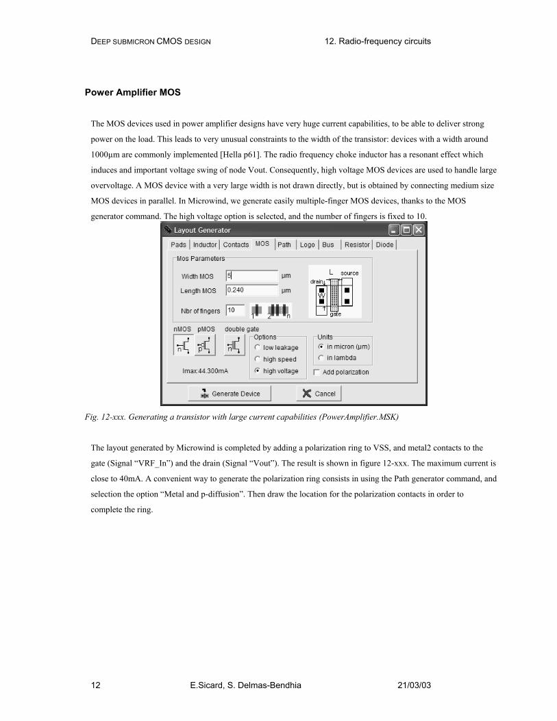
Power Amplifier MOS
The MOS devices used in power amplifier designs have very huge current capabilities, to be able to deliver strong
power on the load. This leads to very unusual constraints to the width of the transistor: devices with a width around
1000µm are commonly implemented [Hella p61]. The radio frequency choke inductor has a resonant effect which
induces and important voltage swing of node Vout. Consequently, high voltage MOS devices are used to handle large
overvoltage. A MOS device with a very large width is not drawn directly, but is obtained by connecting medium size
MOS devices in parallel. In Microwind, we generate easily multiple-finger MOS devices, thanks to the MOS
generator command. The high voltage option is selected, and the number of fingers is fixed to 10.
Fig. 12-xxx. Generating a transistor with large current capabilities (PowerAmplifier.MSK)
The layout generated by Microwind is completed by adding a polarization ring to VSS, and metal2 contacts to the
gate (Signal “VRF_In”) and the drain (Signal “Vout”). The result is shown in figure 12-xxx. The maximum current is
close to 40mA. A convenient way to generate the polarization ring consists in using the Path generator command, and
selection the option “Metal and p-diffusion”. Then draw the location for the polarization contacts in order to
complete the ring.

DEEP SUBMICRON CMOS DESIGN 12. Radio-frequency circuits
13 E.Sicard, S. Delmas-Bendhia 21/03/03
Fig. 12-xxx. The layout of the power MOS also includes a polarization ring, and the contacts to metal2 connections to
VRF_in and VOut (PowerAmplifier.MSK)
Fig. 12-xxx. The layout of a 160mA power MOS using four large MOS in parallel (PowerAmplifierBig.MSK)

DEEP SUBMICRON CMOS DESIGN 12. Radio-frequency circuits
14 E.Sicard, S. Delmas-Bendhia 21/03/03
Fig. 12-xxx. The static characteristics of the 160mA power MOS (PowerAmplifierBig.MSK)
An example of 160mA power device is shown in figure 12-xxx. Four devices are connected in parallel. The output
node drives a large current and must be designed as wide as possible, with a short connection to the output pad, to
limit the serial resistance and parasitic capacitor to ground. The ESD protection is removed in some cases, to enhance
the power amplifier performances [Hella p62]. The ground connection also drives a strong current and must be
carefully connected to the ground supply.
Power Amplifier Efficiency
One of the most important characteristic of the power amplifier is the power efficiency, also called "drain efficiency"
[Lee p348]. The definition of drain efficiency is given by equation 12-xxx. The power efficiency is a ratio, usually
given in %. Typical PE range from 25 to 50%.
P
P PE
DC
outRF _==η (Equ 12-xxx)
Where
PRF_out is the RF output power (in watt)
PDC is the total power delivered from the supply (in watt)

DEEP SUBMICRON CMOS DESIGN 12. Radio-frequency circuits
15 E.Sicard, S. Delmas-Bendhia 21/03/03
We may evaluate the power efficiency of the power amplifier with Microwind, using the following simulation
procedure. The power amplifier is designed with a virtual load (RL=50 ohm in the case of figure 12-xxx). Notice that
the connection of the RL virtual load is unusual: one end of the resistor is connected to VDD rather than VSS.
Connecting RL to ground would add a very important standby DC current, flowing through RL even without RF
input. In reality, the RL resistor represents the antenna radiation resistance which has no direct path to ground.
Fig. 12-xxx. The evaluation of the power amplifier efficiency (PowerAmp.SCH)
By default, the power PDC is computed at each simulation and appears at the right lower corner of the simulation
window of Microwind. In the "Current And Voltage vs. time", we select the current flowing in R(50ohm). At the end
of the simulation, the evaluation of the power efficiency is also displayed.
Fig. 12-xxx. The evaluation of the power amplifier efficiency (PowerAmplifierEfficiency.MSK)

DEEP SUBMICRON CMOS DESIGN 12. Radio-frequency circuits
16 E.Sicard, S. Delmas-Bendhia 21/03/03
Select the current flowing within R(50ohm)
Peff is around 2.5%
Fig. 12-xxx. The evaluation of the power amplifier efficiency is accessible in the " Voltage and Current vs. Time "
mode, by selecting the virtual load (PowerAmplifierEfficiency.MSK)
From the simulation of the simple power amplifier, we obtain a power efficiency of 2.5%, which is very low. In other
words, 97.5% of the supply energy is dissipated and lost in the circuit, with only 2.5% delivered to the load. There
are several techniques to improve the power efficiency: increase the MOS size, modify the amplitude of the input
sinusoidal wave, and modify the DC offset of the input sinusoidal wave.
An other metric for the power amplifier efficiency is the power added efficiency or PAE [Hella p17]. The PAE is
very similar to equation 12-xxx. It includes the input power PRF_in as given in equation 12-xxx. Microwind do not
evaluate directly this parameter.
) P
PP ( PAE
DC
inRFoutRF __ −= (Equ 12-xxx)
Where
PRF_out is the RF output power (in watt)
PRF_in is the RF input power (in watt)
PDC is the total power delivered from the supply (in watt)
Class A Power Amplifier

DEEP SUBMICRON CMOS DESIGN 12. Radio-frequency circuits
17 E.Sicard, S. Delmas-Bendhia 21/03/03
The distinction between class A,B,AB, etc.. amplifiers is mainly given with the polarization of the input signal. A
Class A amplifier is polarized in such a way that the transistor is always conducting. The MOS device operates
almost linearly. An example of power amplifier polarized in class A is shown in figure 12-xxx. The power MOS is
designed very big to improve the power efficiency.
Fig. 12-xxx. The class A amplifier design with a very large MOS device (PowerAmplifierClassA.MSK)
The sinusoidal input offset is 1.3V, the amplitude is 0.4V. The power MOS functional point trajectory is plotted in
figure 12-xxx, using the command "Simulate on Layout". We clearly see the Vgs central point around 1.3V, varying
from 0.9V to 1.7V. The IDS fluctuation is between 20mA to 70mA. The MOS device is also conducting, which
corresponds to class A amplifiers.

DEEP SUBMICRON CMOS DESIGN 12. Radio-frequency circuits
18 E.Sicard, S. Delmas-Bendhia 21/03/03
Fig. 12-xxx. The class A amplifier has a sinusoidal input (PowerAmplifierClassA.MSK)
The main drawback of Class A amplifiers is the high bias current, leading to a poor efficiency. In other words, most
of the power P0 delivered by the supply is dissipated inefficiently. The power efficiency is around 11% in this layout.
The main advantage is the amplifier linearity, which is illustrated by a quasi-sinusoidal output Vout, as seen in figure
12-xxx.
Fig. 12-xxx. The Class A Amplifier simulation (PowerAmplifierClassA.MSK)

DEEP SUBMICRON CMOS DESIGN 12. Radio-frequency circuits
19 E.Sicard, S. Delmas-Bendhia 21/03/03
Class B Amplifier In class B, the MOS device only conducts for half a cycle. The monitoring of the current flowing in the power MOS
shows a peak of current during half the input period. During the other half, the power MOS is off, and the LC
resonator transmits the power to the 50 ohm load. The power efficiency rises to 20%. The main drawback is the
severe distortion of the output voltage, which was much less visible on the class A polarization. The intermediate
class, called AB, corresponds to a conduction between half and the full cycle.
Fig. 12-xxx. The class distinction for the power amplifier is linked to the DC value of the input signal
An evaluation of the spectral contents of the output node may be performed by the Fourier transform, with a plot in
logarithmic scale. A noticeable energy is found on the second harmonic (2.f0=4900MHz) and third harmonic (3.f0),
as shown in figure 12-xxx.

DEEP SUBMICRON CMOS DESIGN 12. Radio-frequency circuits
20 E.Sicard, S. Delmas-Bendhia 21/03/03
Fig. 12-xxx. The class B amplifier is less linear than class A amplifier (PowerAmplifierClassB.MSK)
Other classes In class C, the conduction occurs during less than half the cycle. The increase of efficiency obtained by reducing the
conduction period is achieved at the expense of a reduced output power delivered to the load. The class E amplifier
schematic diagram is shown in figure 12-xxx. A band pass filter (LHF, CHF) is added to the output stage, fitted to the
VRFin input frequency. The power stage is coupled to the resonator through a coupling capacitor Cc. The role of Cc
is to transfer the energy to the load, without any DC path between the supply and the load. The MOS drain can reach
very high values when the switch is OFF. Consequently, a high breakdown voltage transistor is required. The
theoretical efficiency of class E amplifier is higher than 50%.
Fig. 12-xxx. A Class E amplifier (PowerAmpl.SCH)
Self Heating

DEEP SUBMICRON CMOS DESIGN 12. Radio-frequency circuits
21 E.Sicard, S. Delmas-Bendhia 21/03/03
Self heating refers to the temperature rise that can occur in power devices, due to excessive heat energy accumulated
before being dissipated through the substrate, the package and ultimately through the air. The thermal time constant
is the order of one micro-second. Simulations usually consider a typical temperature of 25°C. This is realistic in the
case of low power dissipation (Some milli-watts). In the case of hundreds of milliwatts, the simulation show take in
account a significant temperature rise near the device. For example, a temperature of 80°C is commonly considered in
medium power devices (Below 1W). In some cases, the IC may operate up to 250°C. In Microwind, the operating
temperature may be changed in the menu "Simulator Parameters" of the "Simulate" menu. In the window shown in
figure 12-xxx, the temperature is fixed to 85°C.
Fig. 12-xxx. Setting up a high temperature for analog simulation
12.4 Oscillators
Oscillators create a stable c frequency
Ring Oscillator
The ring oscillator is a very simple oscillator circuit, based on the switching delay existing between the input and
output of an inverter. If we connect a odd chain of inverters, we obtain a natural oscillation, with a performance
which corresponds roughly to the invert of the number of delays. The fastest oscillation is obtained with 3 inverters
(One single inverter connected to itself do not oscillate). The usual implementation consists in 5 to one hundred
chained inverters, with one inverter replaced by a NAND gate to control the oscillation (Figure 12-xxx).

DEEP SUBMICRON CMOS DESIGN 12. Radio-frequency circuits
22 E.Sicard, S. Delmas-Bendhia 21/03/03
Fig. 12-xxx: A ring oscillator is based on an odd number of inverters (Inv3.SCH)
Fig. 12-xxx: The implementation of a 3-inverter oscillator (Inv3.MSK)

DEEP SUBMICRON CMOS DESIGN 12. Radio-frequency circuits
23 E.Sicard, S. Delmas-Bendhia 21/03/03
Fig. 12-xxx: The simulation of the 3-inverter ring oscillator (Inv3.MSK)
The 3-inverter ring-oscillator layout is shown in figure 12-xxx. The right-most inverter output is connect the left-most
inverter input to create the feedback. Notice that no clock is assigned in this layout as the oscillation appears
naturally. The simulation of figure 12-xxx shows the "warm-up" of the inverter circuit followed by a stable frequency
oscillation.
The main problem of this type of oscillator is the very strong dependence of the output frequency with virtually all
process parameters and operating conditions . As an example, power supply voltage VDD has a very significant
importance on the oscillating frequency. This dependency can be analyzed using the parametric analysis in the
Analysis menu. Several simulations are performed with VDD varying from 0.8V to 1.4V with a 50mV step. We
clearly observe a very important increase of the output frequency with VDD (Almost a factor of 2 between the lower
and upper bounds). This means that any supply fluctuation has a significant impact on the oscillator frequency.
Fig. 12-xxx: The oscillator frequency variation with the power supply (Inv3.MSK)

DEEP SUBMICRON CMOS DESIGN 12. Radio-frequency circuits
24 E.Sicard, S. Delmas-Bendhia 21/03/03
Fig. 12-xxx: The process variations also have a direct impact on the switching frequency (Inv3.MSK)
The oscillation frequency of the ring oscillator is not stable, not controllable, and somehow not precisely predictable,
as it is based on the switching characteristics of logic gates, which may fluctuate +/-20%. A Monte Carlo analysis is
performed in figure 12-xxx, again using the parametric analysis. The basic principles of this analysis is to sort in a
random way a set of technological parameters, and conduct the simulation. Each point in the X axis corresponds to
one simulation, with a specific set of parameters. In Microwind, the threshold and mobility parameters are varying
with a Normal distribution, with a typical variation of 10%. We observe again, in figure 12-xxx, the significant
fluctuation of the oscillator frequency. As a conclusion, ring oscillators have poor performances, and may only be
used in low performance clocking systems.
LC oscillator
The LC oscillator proposed in this paragraph is not based on the logic delay, as for the ring oscillator, but on the
resonant effect of a passive inductor and capacitor circuit. In the schematic diagram of figure 12-xxx, the inductor L1
resonates with the capacitor C1 connected to S1 and C2 connected to S2.

DEEP SUBMICRON CMOS DESIGN 12. Radio-frequency circuits
25 E.Sicard, S. Delmas-Bendhia 21/03/03
Fig. 12-xxx. A differential oscillator using an inductor and companion capacitor (OscillatorDiff.SCH)
The layout implementation is performed using virtual inductor and capacitor. This technique is recommended to tune
the passive element values to achieve the correct behavior, before attempting to implement physically theses
components. The time-domain simulation shows a warm-up period where the DC supply rises to its nominal value,
and the oscillator effect which reaches a permanent state after some nano-seconds. The measured frequency is
approaching 3.75GHz.

DEEP SUBMICRON CMOS DESIGN 12. Radio-frequency circuits
26 E.Sicard, S. Delmas-Bendhia 21/03/03
Fig. 12-xxx. A differential oscillator using an on-chip inductor of 3nH (OscillatorDiff.MSK)
DC current isestablished
Oscillationstarts
Permanentregime
Fig. 12-xxx. A differential oscillator using an on-chip inductor of 3nH (OscillatorDiff.MSK)
0.9V, 100°C
1.2V, 27°C
2.f0f0 3.f0
Fig. 12-xxx. The frequency spectrum of the oscillator reveals a main contribution at f0=3.725GHz and some harmonic
contains at 2.f0 and 3f0 (OscillatorDiff.MSK)
We investigate the effect of VDD on the resonating frequency by lowering manually VDD from 1.2V down to 0.9V in
the menu "Simulate"->"Simulation parameters". The result is a significant increase of the warm-up phase, while the
final oscillation frequency remains unchanged. A parametric analysis on VDD, from 0.7 to 1.4V, confirms that the LC
oscillator performs much better than the ring-inverter oscillator, as it reveals to be almost immune to supply voltage
fluctuations.

DEEP SUBMICRON CMOS DESIGN 12. Radio-frequency circuits
27 E.Sicard, S. Delmas-Bendhia 21/03/03
Fig. 12-xxx. The frequency of the LC oscillator is not influenced by the supply voltage VDD (OscillatorDiff.MSK)
The inductance of an on-chip coil is not perfectly predictable, as the material resistance, conductor width and oxide
thickness may vary several %. The capacitance of a poly/poly2 structure, used for implementing the passive capacitor,
may also vary due to the process fluctuation impact on the inter-layer oxide. In Microwind, the Monte-carlo simulation
mode also impacts the value of all virtual elements in a similar way as for the threshold voltage and the mobility:
before the simulation starts, the L and C values are assigned a value that fluctuates with a normal distribution around
the user-defined impedance. The result is a significant variation of the oscillator frequency with the process parameters
(Figure 12-xxx).
Fig. 12-xxx. The frequency of the LC oscillator varies with the process parameters, mainly due to the capacitor and
inductor process dependence (OscillatorDiff.MSK)
Voltage Controlled Oscillator

DEEP SUBMICRON CMOS DESIGN 12. Radio-frequency circuits
28 E.Sicard, S. Delmas-Bendhia 21/03/03
The voltage controlled oscillator (VCO) generates a clock with a controllable frequency. The clock may vary
typically +/-30% of its central frequency. The VCO is commonly used for clock generation in phase lock loop
circuits, as described in paragraph 12-xxx. A typical voltage controlled oscillator is shown in figure 12-xxx [Weste
p336] . The "current-started inverter" chain uses a voltage control "Vcontrol" to modify the current that flows in the
N1,P1 branch. The current through N1 is mirrored by N2,N3 and N4. The same current flows in P1. The current
through P1 is mirrored by P2, P2, and P4. Consequently, the change in Vcontrol induces a global change in the
inverter currents, and directly acts on the delay. Usually not only 3 inverters are in the loop. A higher odd number of
stages is commonly implemented, depending on the target oscillating frequency and consumption constraints.
Fig. 12-xxx. Schematic diagram of a voltage controlled oscillator (VCOMos.SCH)
The implementation of the VCO is given in figure 12-xxx. The current mirror is situated on the left. Five inverters
have been designed to create the basic ring oscillator. Then a buffer inverter is situated on the right side of the layout.

DEEP SUBMICRON CMOS DESIGN 12. Radio-frequency circuits
29 E.Sicard, S. Delmas-Bendhia 21/03/03
Fig. 12-xxx. A VCO implementation using 5 chained inverters (VCO.MSK)
Fig. 12-xxx. The access to Frequency vs. time simulation mode
The VCO circuit frequency variation with "Vcontrol" is investigated in figure 12-xxx. A convenient simulation mode
is directly accessible, as illustrated in figure 12-xxx, to display the frequency variations versus time (Upper window),
and all voltage variations on the lower window. The frequency is evaluated on the selected node, which is the output
node "Vhigh" in this case. We observe no oscillation for an input voltage "Vcontrol" lower than 0.5V. Then the VCO
starts to oscillate, but the frequency variation is clearly not linear. The maximum frequency is obtained for the highest
value of "Vcontrol", around 8.4GHz. By increasing the number of inverters and altering the Ion current of the MOS
devices, we may reduce easily the oscillating frequency.

DEEP SUBMICRON CMOS DESIGN 12. Radio-frequency circuits
30 E.Sicard, S. Delmas-Bendhia 21/03/03
Controlvoltage
increased
Oscillationstarts here
Non-lineardependence
Fig. 12-xxx. The frequency variations versus the control voltage show a non-linear dependence (VCO.MSK)
High Performance VCO
A voltage controlled oscillator with good linearity is shown in figure 12-xxx. This circuit has been implemented in
several test-chips with successful results in 0.8, 0.35 down to 0.18µm technologies. The principles of this VCO is a
delay cell with linear delay dependence with the control voltage [Bendhia]. The delay cell consists of a p-channel
MOS in series, controlled by "Vcontrol" and a pull-down n-channel MOS, controlled by "Vplage". The delay
dependence with "Vcontrol" is almost linear for the fall edge. The key point is to design an inverter just after the
delay cell with a very low commutation point Vc. The rise edge is almost unchanged. To delay both the rise and fall
edge of the oscillator, two delay cells are connected, as shown in the circuit of figure 12-xxx.

DEEP SUBMICRON CMOS DESIGN 12. Radio-frequency circuits
31 E.Sicard, S. Delmas-Bendhia 21/03/03
Delay cellLow Vcinverter Buffering
Delay circuit forfall edge
Delay circuit forrise edge
Fig. 12-xxx. The layout implementation of a high performance VCO circuit (VCOLinear.MSK)
Fig. 12-xxx. The layout implementation of a high performance VCO circuit (VCOLinear.MSK)
The layout of the VCO is a little usual due to needs for a very low commutation point for the inverter situated
immediately after the delay cells. This is done by implementing a large n-channel MOS with high drive capabilities
and a tiny p-channel MOS with low drive capabilities (Figure 12-xxx).

DEEP SUBMICRON CMOS DESIGN 12. Radio-frequency circuits
32 E.Sicard, S. Delmas-Bendhia 21/03/03
Fig. 12-xxx. The low commutation point of the delay cell inverter (InvLowVc.MSK)
Fig. 12-xxx. The simulation of a high performance VCO circuit showing a quasi-linear dependence of the oscillating
frequencyt with the input voltage control (VCOLinear.MSK)
The simulation of a high performance VCO circuit is given in figure 12-xxx. A quasi-linear dependence of the
oscillating frequency with the input voltage control is observed within the range 0..0.6V. The value of the second

DEEP SUBMICRON CMOS DESIGN 12. Radio-frequency circuits
33 E.Sicard, S. Delmas-Bendhia 21/03/03
voltage "Vplage" has a strong influence on the oscillating frequency range. A high value of "Vplage" (Close to VDD)
corresponds to high frequency oscillation, while a low value (Close to the threshold voltage VT) corresponds to a low
frequency oscillation.
The main drawback of this type of oscillator is the great influence of temperature and VDD supply on the stability of
the oscillation. If we change the temperature, the device current changes, and consequently the oscillation frequency
is modified. Such oscillators are rarely used for high stability frequency generator. Other oscillator circuits are
preferred (See section 12.5).
12.5 Phase-Lock Loop
The phase-lock-loop (PLL) is commonly used in microprocessors to generate a clock at high frequency
(Fout=2GHzMHz for example) from an external clock at low frequency (Fref = 100MHz for example). The PLL uses a
counter, which divides a high input frequency Fout into a low output frequency (divide by 32 in the example), which
is tuned to fit exactly with the reference frequency Fref. The basic schematic diagram of this function is reported
below.
Phase detector Filter
High frequencyVoltage controled
oscillator
Highfrequency
Fout = N Fref
Vc
Counterdivide by N
Lowfrequency
signal
Lowfrequency
Fref
pulseclkIn
divIn
clkOut
Fig. 12-xxx. Principles of phase lock loops
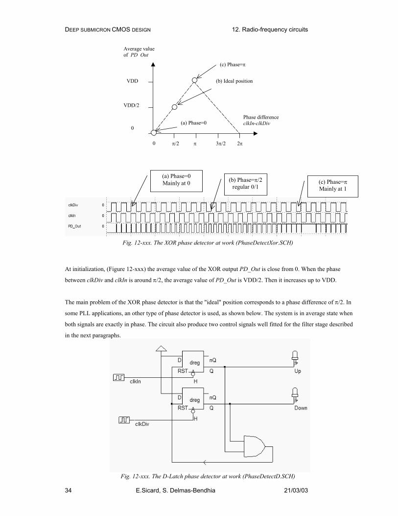
PHASE DETECTOR
The most simple phase detector is the XOR gate. The XOR gate output produces a regular square oscillation PD_Out
when the input clkIn and the signal divIn have one quarter of period shift (or 90° or π/2). For other angles, the output
is no more regular. In figure 12-xxx, two clocks with slightly different periods are used in Dsch2 to illustrate the
phase detection.
DEEP SUBMICRON CMOS DESIGN 12. Radio-frequency circuits
34 E.Sicard, S. Delmas-Bendhia 21/03/03
0
VDD/2
VDD
Average value of PD Out
0 π/2 π 3π/2 2π
Phase difference clkIn-clkDiv
(b) Ideal position
(a) Phase=0
(c) Phase=π
(b) Phase=π/2 regular 0/1
(a) Phase=0Mainly at 0 (c) Phase=π
Mainly at 1
Fig. 12-xxx. The XOR phase detector at work (PhaseDetectXor.SCH)
At initialization, (Figure 12-xxx) the average value of the XOR output PD_Out is close from 0. When the phase
between clkDiv and clkIn is around π/2, the average value of PD_Out is VDD/2. Then it increases up to VDD.
The main problem of the XOR phase detector is that the "ideal" position corresponds to a phase difference of π/2. In
some PLL applications, an other type of phase detector is used, as shown below. The system is in average state when
both signals are exactly in phase. The circuit also produce two control signals well fitted for the filter stage described
in the next paragraphs.
Fig. 12-xxx. The D-Latch phase detector at work (PhaseDetectD.SCH)

DEEP SUBMICRON CMOS DESIGN 12. Radio-frequency circuits
35 E.Sicard, S. Delmas-Bendhia 21/03/03
FILTER
The filter may simply be a large capacitance C, charged and discharged through the Ron resistance of the switch. The
Ron.C delay creates a low-pass filter. Figure 12-xxx shows an XOR gate with output charged with a large poly/poly2
capacitor.
Fig. 12-xxx. Large load capacitance and weak XOR output stage to act as a filter (phaseDetect.MSK)
Fig. 12-xxx. Response of the phase detector to slightly different input clocks (phaseDetect.MSK)

DEEP SUBMICRON CMOS DESIGN 12. Radio-frequency circuits
36 E.Sicard, S. Delmas-Bendhia 21/03/03
In the figure above, the filtered version of the XOR gate output is shown. Although some further filtering are required,
it can be seen that Vc is around VDD/2 when the phase difference is π/2 or -π/2.
Complete Phase Lock Loop
<Text to be added>
<Simulation to be added>
12.6 Frequency Converter
Principles
In many situations for radio frequency emitters and receivers, there is a need for shifting a input waveform into a
lower or higher frequency waveform. From an emission point of view, most of the signal processing is done within
the range 10-100MHz. However, the emission bandwidth may be significantly higher (900MHz, 1.8GHz for mobile,
2.4, 5GHz for wireless local area network). A direct generation of the desired signal at such a high frequency would
consume too much power. A low power frequency translator circuit is preferred. In the case of figure 12-xxx, the
frequency converter shifts the original signal (Say 100MHz) to the desired emission frequency 900MHz.
fin
frequency
amplitude
Fhigh
Up converter
Signal processing at100MHz
Emission at900MHz
Figure 12-xxx: the principles for frequency conversion
The operation which translates a high frequency signal into a low frequency signal is called down conversion. In
frequency domain, it consists in shifting a high frequency information contained in frequency fin to a lower frequency
flow, as illustrated in figure 12-xxx. The information contained in the original signal fin (Which may include an
amplitude, frequency or phase variation) is preserved in the resulting signal fout.

DEEP SUBMICRON CMOS DESIGN 12. Radio-frequency circuits
37 E.Sicard, S. Delmas-Bendhia 21/03/03
time
time
Downconverter
Input signal fin
Low frequency flow
finFlow
Downconverter
frequency
amplitudeamplitude
amplitude
Fhigh
Up converter
time
amplitude
High frequency fhigh
Up converter
Figure 12-xxx: the principles for frequency conversion
Adding sinusoidal waves
Adding sinusoidal waves is very easy. A simple circuit containing 3 resistor produces the addition of two sinusoidal
waves, as shown in figure 12-xxx. The formulation is easily demonstrated using the superposition theorem.
[ ]ttVout 21 coscos31 ωω += (Equ. 12-xxx)
Figure 12-xxx: Adding sinusoidal waves is easy, a set of 3 resistors is sufficient to build the sum (AddSinus.MSK)

DEEP SUBMICRON CMOS DESIGN 12. Radio-frequency circuits
38 E.Sicard, S. Delmas-Bendhia 21/03/03
Figure 12-xxx: The simulation of the sinusoidal wave adder (AddSinus.MSK)
The Fourier transform of the signal s1+s2 reveals two harmonics, one at the frequency of signal 1, the other at the
frequency of signal 2, as the formulation 12-xxx suggested. Clearly, no frequency shift may be obtained using
sinusoidal addition.
Figure 12-xxx: The Fourier transform of s1+s2 reveals two harmonics, one at 100MHz the other at 1GHz
(AddSinus.MSK)
Multiplying sinusoidal waves
At the core of up/down frequency conversion is the multiplication of two sinusoidal waves in the time domain [Lee
Chapter 12]. The result of that multiplication is the generation of two new frequencies: one at the sum of frequency,
one for the difference.

DEEP SUBMICRON CMOS DESIGN 12. Radio-frequency circuits
39 E.Sicard, S. Delmas-Bendhia 21/03/03
[ ]tttt )sin()sin(21)sin().sin( 212121 ωωωωωω +−−= (Equ. 12-xxx)
where
ω1=2π.f1
ω2=2π.f2
f1 = frequency of signal 1 (Hz)
f2 = frequency of signal 2 (Hz)
If we consider a low frequency fin, and a high frequency fOsc and only consider absolute values, the multiplication
of these two sinusoidal signals creates two new sinusoidal contributions: one at fOsc-fin, one at fOsc+fin (Figure 12-
xxx). Using an LC resonant circuit, we only keep the desired frequency contribution. In the case of figure 12-xxx,
the L and C values are tuned to highlight the fOsc+fin contribution, which fits with the emission bandwidth. The LC
resonator also serves as a filter of undesired harmonics, such as fOsc-fin and fOsc.
fin fOsc
frequency
amplitude
Up converter
fin
fOSC
fOsc+ fin, fOsc -fin
fOsc -finfOsc +fin
fin
amplitude
Resonator
fOsc +fin
frequency
Only keep fOsc +fin
LC resonnance
Attenuation ofundesired
frequencies
Emissionbandwidth
Figure 12-xxx: The multiplication of two frequencies create new frequency components
Using a MOS for Sinus Multiplication
The process for multiplying signals with CMOS devices is far from being simple. The nMOS and pMOS are non-
linear devices. The best example is the long channel nMOS which gives approximately a square law dependence
between Vgs-Vt and Ids (See chapter 3 for more details about device modeling). A linear device would give a linear
dependence between Ids and Vgs, which is almost the case for short-channel devices.

DEEP SUBMICRON CMOS DESIGN 12. Radio-frequency circuits
40 E.Sicard, S. Delmas-Bendhia 21/03/03
Linear Vgsincrease (200mV)
Non-linear Ids increase(square law)
Figure 12-xxx: The long-channel MOS characteristics exhibit a square dependence of Ids vs. Vgs (MixerMos.MSK)
The idea is as follows (Figure 12-xxx): the two sinusoidal inputs fIn and fOsc are added on the gate Vgs. The current
Ids is a non linear function of Vgs. The static characteristics of the device (W=50µm, L=0.5µm) show a "quadratic"
dependence: each Vgs step induces a non-linear increase of Ids. This can be simply written as:
2).( VtVkI GSDS −≈ (Equ. 12-xxx)
where
k depends on the design and technology
Vt is the threshold voltage (Around 0.35V)
fin fOsc
frequency
Ids
fin
fOSC
fOsc -finfOsc +fin
2.fOsc
Harmonics of fin
Harmonic ofinterestIds
Figure 12-xxx: The Ids current exhibits several harmoniccs, including the desired high frequency fOsc+fin
(MixerMos.MSK)
If Vgs is a sum of sinusoidal waveforms, as we did in the previous section, the current may be written as:

DEEP SUBMICRON CMOS DESIGN 12. Radio-frequency circuits
41 E.Sicard, S. Delmas-Bendhia 21/03/03
[ ]2)sin()sin(.. VttvtvVkI oscoscininbiasDS −++≈ ωω (Equ. 12-xx)
[ ])sin.(sin..10 ttvvkII inoscoscinDSDS ωω+≈ (Equ. 12-xx)
[ ]ttvvk
II inoscinoscoscinDSDS )sin()sin(..21
0 ωωωω −−++≈ (Equ. 12-xx)
The most important result beyond this approximation is that the input signal and the oscillator signal are effectively
multiplied and create the desired harmonics. In other words, passing a sum of sinusoidal waveforms into a non-linear
device create several harmonics, including the multiplication of the sinusoidal waveforms. The desired harmonic is
underlined in equation 12-xxx, and corresponds the the harmonic of interest of figure 12-xxx. The term Ids0 also
contains the original input signal, the oscillator signal and all their respective harmonics too, which lead to a quite
complex output. A band-pass filter is mandatory to eliminate undesired harmonics and amplify the desired signal.
The circuit is called a single-balanced mixer.
Layout Implementation
The n-channel MOS implemented in the mixer layout must have a large length to eliminate short channel effects and
exhibit a square law dependence between Vgs and Ids. This is the case of MOS devices with a length larger than
0.5µm. A resistance load is mandatory to perform amplification. The resistor is matched to the Ron resistance of the
nMOS device. The input is the sum of two sinusoidal components, through a resistor bridge.
Figure 12-xxx: Building a single-balanced mixer with a n-channel MOS device (MixerMos.SCH)

DEEP SUBMICRON CMOS DESIGN 12. Radio-frequency circuits
42 E.Sicard, S. Delmas-Bendhia 21/03/03
Figure 12-xxx: Design of a mixer using a large width, large length nMOS device, with a sum of sinusoidal waves at the
input (MixerMos.MSK)
According to the theory, the time-domain simulation of the mixer reveals that the Vout signal has a very complex
aspect.

DEEP SUBMICRON CMOS DESIGN 12. Radio-frequency circuits
43 E.Sicard, S. Delmas-Bendhia 21/03/03
Figure 12-xxx: Simulation of the mixer with a 450Mhz and 2Ghz added inputs (MixerMos.MSK)
The Fourier Transform is obtained by a click on "FFT" in the simulation window. The 450MHz input signal, the
2GHz oscillator signal, as well as the harmonics and products are present in the spectrum. The only desired harmonic
is the 2.45GHz contribution, corresponding to fin+fosc.
fin at 450MHz
foscat 2000MHz
2.fin
Desired signal at fin+fosc (2450MHz)

DEEP SUBMICRON CMOS DESIGN 12. Radio-frequency circuits
44 E.Sicard, S. Delmas-Bendhia 21/03/03
Figure 12-xxx: The output voltage includes fin, fosc and their corresponding harmonics. The desired signal is at
fosc+fin (MixerMos.MSK)
Mixer with LC resonator
The mixer shown in figure 12-xxx has two important features: the serial resistor is replaced by an inductor LHF of
3nH, and a capacitor CHF=1.2pF is added to the output. The LC resonator formed by the inductor LHF and the
capacitor CHF matches the target frequency 2.45GHz (Use the resonant frequency evaluator in the Analysis menu to
confirm). The serial resistor RL accounts for the finite quality of the inductor, and corresponds to the long metal wire
resistance of the physical inductor. Removing this serial resistor would create overestimated oscillations, possibly
numerical instability, and the results could not be exploited.
Figure 12-xxx: The schematic diagram of a mixer with a LC resonator tuned to 2.45GHz
The mixer implementation was not completely performed in the layout of figure 12-xxx. For simplicity, we used
virtual L and C rather than a physical inductor. The 3nH inductor is placed in series with a parasitic resistance, to
limit the LC resonance effect. The capacitor 1.2pF is also virtual, and is placed near "Vout".
The Fourier transform of the time-domain simulation is proposed in figure 12-xxx, and corresponds to the output
node "Vout". The desired signal at 2.45GHz appears much more clearly than in figure 12-xxx, which validates the
pass-band effect of the LC resonator. Unfortunately, the selectivity of the LC circuit is not enough to erase the
oscillator frequency at 2GHz. Residues of other harmonics also appear in the Fourier transform: 1.6GHz, 4GHz.

DEEP SUBMICRON CMOS DESIGN 12. Radio-frequency circuits
45 E.Sicard, S. Delmas-Bendhia 21/03/03
Figure 12-xxx: The mixer with a tuned LC resonator targeted to 2.45GHz (MixerLC.MSK)
Figure 12-xxx: The Fourier transform of Vout shows a main contribution at the desired frequency and residues of
other harmonics (MixerLC.MSK)
An increase of the input frequency fin is translated into a corresponding increase of the output frequency. For
example, a slow increase in fin shifts the main peak to the right in a proportional way. Also, an increase of the
amplitude of fin induces a corresponding increase of the 2.45GHz harmonic.

DEEP SUBMICRON CMOS DESIGN 12. Radio-frequency circuits
46 E.Sicard, S. Delmas-Bendhia 21/03/03
The little increase of f isprovoked by a non-nullvalue at this location
The sinusIn signal starts at alower frequency (400instead of 450MHz)
Figure 12-xxx: The input SinusIn starts from 400MHz and slowly rises to 500MHz (MixerLC.MSK)
Figure 12-xxx: A little increase of the input frequency is translated into an increase of the main harmonic
(MixerLC.MSK)
Double-balanced Mixer
The main drawback of the mixer output provided by the LC mixer is the important amount of parasitic signals added
to the desired signal. The undesired signals 2.55GHz (fosc-fin), 2GHz (fosc), 2.9GHz (fosc+2.fin), 4GHz (2.fosc),
also clearly appear in the spectrum. A very brilliant idea would consist in creating two signals where all harmonics
would be in opposite phase except the desired harmonics which would be in phase. Adding these two signals would
create a miraculous signal with fosc+fin and fosc-fin.

DEEP SUBMICRON CMOS DESIGN 12. Radio-frequency circuits
47 E.Sicard, S. Delmas-Bendhia 21/03/03
Figure 12-xxx: Implementation of the double-balanced mixer (MixerDoubleLC.SCH)
A circuit that realizes this function is proposed in figure 12-xxx. The "vin" signal and "Vosc" signal are combined as
seen previously, in the left branch of the mixer, on the gate of the n-MOS device. The output produces several
harmonics. The LC resonator highlights the contributions near 2.45GHz.
[ ]21 )sin()sin(.. VttvtvVkI oscoscininbiasDS −++≈ ωω (Equ. 12-xx)
ids2=k[Vbias-vinsin(t)-voscsin(wosct)-Vt]2
Ids1+Ids2=k[Ids0+2vin.sin(wosc+win)t+2vin.vosc.sin(wosc-win)t
The remarkable point that can be seen in equation 12-xxx is that the sum of currents Ids1+Ids2 that flows in the
50ohm load resistor RL mainly includes the mixer products at frequencies wosc+win and wosc-win, which was
exactly the goal of the mixer.

DEEP SUBMICRON CMOS DESIGN 12. Radio-frequency circuits
48 E.Sicard, S. Delmas-Bendhia 21/03/03
Figure 12-xxx: Layout of the double-balanced mixer (MixerDoubleLC.MSK)
The layout implementation makes an extensive use of virtual R,L,C elements. This technique is recommended for the
tuning of the circuit, but one should remember that the final goal is a complete layout implementation. The simulation
performed in figure 12-xxx confirms the theoretical assumption: the Fourier transform clearly includes the two main
contributions near 1500MHz and 2500Mhz, without wosc in between. Removing the undesired harmonics is quite
easy, in order to keep the desired 2500MHz contribution. When the fin frequency is increased, the output harmonic at
fin+fosc is increased, and the fin-fosc harmonic is decreased.
Figure 12-xxx: Fourier transform of the double-balanced mixer output (MixerDoubleLC.MSK)
Gilbert Mixer

DEEP SUBMICRON CMOS DESIGN 12. Radio-frequency circuits
49 E.Sicard, S. Delmas-Bendhia 21/03/03
Figure 12-xxx: The Gilbert mixer (MixerGilbert.SCH)
The double-balanced mixer shown in figure 12-xxx is not implemented as it. In reality, mixers use the Gilbert cell
(Invented by Barry Gilbert [Reference]), which consists of only six transistors, and performs a high quality
multiplication of the sinusoidal waves [Lee p323]. The schematic diagram shown in figure 12-xxx uses the tuned
inductor as loads, so that Vout and ~Vout oscillate around the supply VDD.
Figure 12-xxx: The Gilbert mixer implementation with virtual R,L and C (MixerGilbert.MSK)

DEEP SUBMICRON CMOS DESIGN 12. Radio-frequency circuits
50 E.Sicard, S. Delmas-Bendhia 21/03/03
Figure 12-xxx: Time-domain simulation of the Gilbert mixer (MixerGilbert.MSK)
The implementation shown in figure 12-xxx makes again an extensive use of virtual R,L and C elements. The 3nH
inductor is in series with a parasitic 5 ohm resistance, on both branches. The time domain simulation reveals a
transient period from 0.0 to 8ns during which the inductor and capacitor warm-up. This initialization period is not of
key interest. The most interesting part starts from 8ns, where the output Vout and Vout2 are stable, and oscillate in
opposite phase around 2.5V.
Figure 12-xxx: Fourier transform of the Gilbert mixer output (MixerGilbert.MSK)

DEEP SUBMICRON CMOS DESIGN 12. Radio-frequency circuits
51 E.Sicard, S. Delmas-Bendhia 21/03/03
The Fourier transform of nodes Vout and Vout2 are almost identical. We present the Fourier transform in logarithm
scale to reveal the small harmonic contributions. As expected, the 2GHz Fosc signal and 450MHz fin signals have
disappeared, thanks to the cancellation of contributions. The two major contributors are fosc+fin and fosc-fin.
Notice that the simulation time has an influence on the Fourier Transform result: a short simulation (5ns) would a
poor precision in our frequency range of interest, but a high precision on very high frequencies (Above 10GHz). In
our case, il is preferable to peform the time domain simulation over a large time (50ns) which will give a high
precision at low frequencies (From DC to 5GHz), but limit the Fourier spectrum to around 10GHz. As the target
frequency is around 2.5GHz, a long simulation gives the best results, as shown in figure 12-xxx. 3nH coils
6 ohm serial resistance
On-chip capa for tuning Mixer devices
Figure 12-xxx: The complete implementation of a Gilbert mixer circuit (MixerGilbert2.MSK)
In figure 12-xxx, a complete implementation of the Gilbert mixer has been realized, so that virtual R,L and C
components are replaced by physical elements. The coils have a target 3nH inductance, and their associated parasitic
resistance is approaching 6 ohm when the combination of metal6,metal5 and metal4 are used. The tuning capacitor is
added to the parasitic coil capacitor to perform the best resonance at the desired 2.5GHz frequency. The design relies
on good models for the inductor and capacitor, which is not the case in the Microwind software, which uses first
order approximations of parasitic resistance, capacitance and coil inductance. In a real case implementation, we may
expect significant differences between measurements and simulations. Having accurate predictions of such circuits is
quite challenging.
12.7 Sub-sampling Frequency Converter

DEEP SUBMICRON CMOS DESIGN 12. Radio-frequency circuits
52 E.Sicard, S. Delmas-Bendhia 21/03/03
time
time
Downconverter
High frequency fin
Low frequency fout
finfout
Downconverter
frequency
amplitudeamplitude
amplitude
Fig. 12-xxx: Principles for down conversion
One very simple solution consists in using a transmission gate with a very accurate tuning of the gate clock. As an
illustration, we use a 1.900 GHz sinusoidal wave, and a 1.818 Ghz sampling signal (550 ps period). The expected
output frequency is therefore 1.900-1.818=0.082 GHz, that is 82MHz. The layout of the sample circuit is a simple
transmission gate with an RC filter (Figure 12-xxx).
Fig. 12-xxx. Layout of the transmission gate and RC filter used for down conversion (DownConverter.MSK)

DEEP SUBMICRON CMOS DESIGN 12. Radio-frequency circuits
53 E.Sicard, S. Delmas-Bendhia 21/03/03
Fig. 12-xxx. Down conversion of the 1.9GHz input sinusoidal wave to a low frequency
The sampling at a frequency slightly slower than the input frequency leads to a signal at low frequency at the
output of the transmission gate. (Figure 12-xxx). With a simple RC filtering, the output signal becomes a
sinusoidal wave with a frequency equal to the difference of the initial waveform and the gate control
frequency. When simulating at a large time scale (Figure 12-xxxx), and asking for the evaluation of the
frequency of the resulting waveform, we find 83MHz, very close from the expected 82MHz resulting from
the subtraction 1900 MHz-1818MHz.
In figure 12-xxx, the effect of filtering is clearly seen. The spikes have disappeared, and a clean sinusoidal
waveform remains.
Fig. 12-xxx. Down conversion of the 1.9GHz input sinusoidal wave to 83MHz

DEEP SUBMICRON CMOS DESIGN 12. Radio-frequency circuits
54 E.Sicard, S. Delmas-Bendhia 21/03/03
12.8 Noise in RF Circuits
<Goyal p185>
-1xxx
-170
Hz/dBV
Frequency ( Hz)102108
White noisedominates
1/f noisedominates
104 1061010
Figure 11-xxx: Noise power spectral desnity versus frequency for a MOS device
12.9 Conclusion
References
[Macnamara] Macnamara T. "Handbook of Antennas for EMC", Artech House Publishers, ISBN 0-89006-549-7
[Weste] Neil H. E. Weste, Kamran Eschraghian "Principles of CMOS VLSI Design", Addison-Wesley, 1993, ISBN
0-201-53376-6
[xxx] Niknejad Ali M., Meyer, robert G. "Design, simulation and applications of Inductors and Transfromers for Si
RF Ics", Kluwer, 2000, Isbn 0-7923-7986-1
[Lee] T.H.Lee "The Design of Radio-frequency Integrated Circuits”, Cambridge University Press, 1998, ISBN 0-
521-63061-4
[xxx] H. A. Wheeler "Simple Inductance Formulas for Radio Coils”, Proceedings of the IRE, Oct. 1928, pp 1398-
1400
[xxx] M. Thompson “Inductance Calculation Techniques – Part II: Approximations and Handbook Methods”, Power
Control & Intelligent Motion, Dec 1999
[Hella] Mona M. Hella, Mohammed Ismail “RF CMOS power Amplifiers, theory, Design and Iomplementation”,
Kluwer academic publishers, 2002, ISBN 0-7923-7628-5

DEEP SUBMICRON CMOS DESIGN 12. Radio-frequency circuits
55 E.Sicard, S. Delmas-Bendhia 21/03/03
[Bendhia] Sonia Bendhia "xxx" Delay cell reference
Exercises