radio science advances in towards a generic operational ... · scopic operational amplifier. the...
TRANSCRIPT
Adv. Radio Sci., 4, 259–262, 2006www.adv-radio-sci.net/4/259/2006/© Author(s) 2006. This work is licensedunder a Creative Commons License.
Advances inRadio Science
Towards a generic operational amplifier with dynamicreconfiguration capability
S. K. Lakshmanan and A. Koenig
Institute of Integrated Sensor Systems, TU-Kaiserslautern, Germany
Abstract. Analog and analog-digital mixed signal electron-ics needed for sensor systems are indispensable componentswhich tend to drifts from the normal phase of operation dueto the impact of manufacturing conditions and environmentalinfluences like etching, aging etc. Precise design methodol-ogy, trimming / calibration are essential to restore function-ality of the system. Recent block level granular approachesusing Field Programmable Analog Array and the more recentapproaches from evolutionary electronics providing transis-tor level granularity using Field Programmable TransistorArrays offers considerable extensions. In our work, westarted on a new medium granular level approach calledField Programmable medium-granular Mixed-signal Array(FPMA) providing basic building blocks of heterogeneousarray of active and passive devices to configure establishedcircuit structures which are adaptive, biologically inspiredand dynamically re-configurable. Our design objective is tocreate components of clear compatibility to that of the in-dustrial standards having predictable behavior along with theincorporation of existing design knowledge. The cells can beused in as a single instance or multiple instances. Further, wewill focus on a generic dynamic reconfigurable amplifier cellwith flexible topology and dimension called Generic Opera-tional Amplifier (GOPA). The incentive of our work comesfrom recent development in the field of measurement and in-strumentation. The digital programming of analog devices iscarried out using range of algorithms from simple to evolu-tionary. Physical realization of the basic cells is carried outin 0.35µm CMOS technology.
1 Introduction
Primary sensor and mixed signal electronics are indispens-able components, which are subjected to strong manufac-
Correspondence to:S. K. Lakshmanan([email protected])
turing conditions and environmental influences like etching,doping concentration, ageing etc. Subsequently the systemtends to drift from its normal functionality. In order to reducethe substantial impact of the undesirable conditions or influ-ences, usual approaches employ trimming / calibration andcareful matched layouts during production time (Analog De-vices, 2004). The counter measures adapted helps to restorethe functionality of the system. The so adapted conservativeprocedures are slow, static, expensive, and have to be per-formed repeatedly, if dynamic. More improved approachesadapt these established procedures by compensation tech-niques during actual working phase in the name of self di-agnosis / self-calibration. Block level granular approach en-titled Field Programmable Analog Array (FPAA) uses digi-tally programmable resistors for compensation which are in-terconnected to the whole amplifier blocks (Fruehauf et al.,2002). The field programmable array structures of the com-mercially available Anadigm chip best suites the category.The chip allows interconnection of passive elements withthe amplifier blocks to application specific in time-discretedomain (Anadigm Inc., 2003). More recent approachescomes from the field of evolutionary electronics (Zebulumet al., 2002), where the circuit synthesis are carried outthrough learning procedures by a suitable flexible transistorlevel granular hardware structure called Field ProgrammableTransistor Arrays (FPTA) (Langeheine et al., 2003). Sub-stantial drawbacks here are the fact that optimisation algo-rithm should invent the knowledge of an experienced de-signer, e.g, designing a sensor signal amplifier, uses exces-sive switching resources resulting in large internal memoryconfiguration. These structures also exhibit characteristics ofa black box, where the underlying behaviour remains unfore-seeable. Here the point of preservation is that the quality pa-rameters essential for automatic control comes from a specialflexible structure of hardware, especially dynamic reconfigu-ration. Our research work, focuses on developing a suitable,flexible and dynamically re-configurable hardware structurecalled Field Programmable medium-granular Mixed-signal
Published by Copernicus GmbH on behalf of the URSI Landesausschuss in der Bundesrepublik Deutschland e.V.

260 S. K. Lakshmanan and A. Koenig: Towards a generic operational amplifier with dynamic reconfiguration capability
M1
M2
M3
M4
M13
Gnd
RL
Vdd
Vin -
Vin +
M5 M6
Gnd
Iss
M14
M9
M7
Gnd
M8
M10
M11
M12
s s
s
Transistor
D
FF
D
FF
D
FF
D FF
Shift Register
1 2 4 128
128 s
ss s
s
s
1 2G
D
Digital Device Selection
Scalable S
Fig. 1. Folded Cascode amplifier and the replacement scheme ofordinary by the heterogeneous array / scalable transistors (Laksh-manan and Koenig, 2004).
Array (FPMA) providing a platform for the implementa-tion of algorithms ranging from a simple to the more re-cent organic computing, paving the way in realising thefavourable behaviour or characteristics of living organisms.The favourable characteristics for our interest include self-monitoring, self-testing, self-healing, self-repair, which aregenerally referred to as Self x characteristics. The implemen-tation of the work is carried out in 0.35µm CMOS technol-ogy of Austriamicrosystems provided by EUROPRACTICE.
2 Re-configurable operational amplifier
The approach pursued by our work combines the conceptspresented in the previous section with the objective of build-ing flexible hardware structure suitable for sensor elec-tronics. In our work, we focused on the design and im-plementation of sensor signal amplifier reducing the finegrained homogenous FPTA structure to a suitable mediumgrained heterogeneous structure thereby reducing the switch-ing resources and consequently the parasitic effects of theswitches. The approach also reduces the on chip storage re-quirement and decreases the reconfiguration time comparedto that of its counterpart namely FPTA. The choice of the di-mensions of the basic active and passive elements of the het-erogeneous array are determined by simulations for the cho-sen technology (Lakshmanan and Koenig, 2004) and fromthe inspiration taken from A/D – D/A converters.
The dimensions of the transistors vary in the powers oftwo that are interconnected through switches. The selectionof the appropriate dimension for the switches plays a vitalrole as it has subsequent impact on the overall system per-formance. The selection of active or passive device from thearray are carried out by turning on the switches connectedto their corresponding terminals. The switching patternsare fed sequentially through shift registers. Figure 1 shows
Digital Device Selection
1281 2 4
D
FF
D
FF
Shift Register
D
FF
D
FF
G
s s
s
s
s
ss
s
s
Transistor
1 128 2
Scalable S
Vin+Vin-
Vdd
vo Miller OPA
GOP A
D
Fig. 2. Schematic representation of GOPA realizing miller opera-tional amplifier.
the schematic of the time-continuous sensor signal amplifierwith folded cascode topology using ordinary transistors andtheir corresponding replacement scheme by the scalable tran-sistors / heterogeneous array.
3 Generic operational amplifier - GOPA
In the previous section, realisation of a time continuous sen-sor signal amplifier was carried out. In this section we focuson building a generic amplifier block which is flexible to bothdimensions and topology. GOPA consists of array of scalableactive and passive devices.
The next level hierarchical switches called TopologySwitches (TS) interconnect the heterogeneous arrays. Byswitching ON and OFF these topology switches intercon-necting the scalable array, various established amplifiertopologies are realized ranging from a simple Miller to Tele-scopic operational amplifier. The flexibility is not only re-stricted to two stages but are also extended to three stage am-plifier structures with programmable compensation capaci-tors and nullifying resistors. Some possible building struc-tures of any operational amplifier topology that are realizedby GOPA are simple and cascoded current mirrors, Wilsoncurrent mirror in the tail current region. Diode or currentmirror loaded differential pairs and cascoded output stages.Realization of single ended and differentially ended outputis also realized. The GOPA structure is capable of realiz-ing more than 15 established simulation verified amplifierstructures providing complete flexibility both in the choiceof the structure and in dimensioning the devices constitutingthe structures. Figure 2 represents GOPA structure realizingMiller operational amplifier.
Adv. Radio Sci., 4, 259–262, 2006 www.adv-radio-sci.net/4/259/2006/

S. K. Lakshmanan and A. Koenig: Towards a generic operational amplifier with dynamic reconfiguration capability 261
The next level hierarchical switches called Topology Switches (TS) interconnect the
heterogeneous arrays. By switching ON and OFF these topology switches interconnecting the
scalable array, various established amplifier topologies are realized ranging from a simple
Miller to Telescopic operational amplifier. The flexibility is not only restricted to two stages
but are also extended to three stage amplifier structures with programmable compensation
capacitors and nullifying resistors. Some possible building structures of any operational
amplifier topology that are realized by GOPA are simple and cascoded current mirrors,
Wilson current mirror in the tail current region. Diode or current mirror loaded differential
pairs and cascoded output stages. Realization of single ended and differentially ended output
is also realized. The GOPA structure is capable of realizing more than 15 established
simulation verified amplifier structures providing complete flexibility both in the choice of
the structure and in dimensioning the devices constituting the structures.
4 Implementation
After promising results from the schematic level simulations of the pursued concepts in the
previous sections, are thereafter implemented for a sensor signal amplifier. Fig.3 shows the
layout of the NMOS scalable transistor array along with the digital interface surrounding the.
Figure 3. Layout of NMOS scalable transistors
5
Fig. 3. Layout of NMOS scalable transistors.
4 Implementation
After promising results from the schematic level simula-tions of the pursued concepts in the previous sections, arethereafter implemented for a sensor signal amplifier. Fig.3shows the layout of the NMOS scalable transistor array alongwith the digital interface surrounding the. heterogeneousarray. The layout area of the NMOS scalable transistor is60µm · 64µm. The flexibility does not come for free. Acompromising additional layout area is consumed. The scal-able transistors form the basic building blocks of FPMA. Thearray consists of 11 transistors interconnected by transmis-sion switches. The minimum sized transistors are replicated4 times in order to avoid the effects of mismatching. Theremaining 7 transistors vary in the powers of two. There-fore, a total of 11 switch signal are needed for each scalabletransistor array. The selection of the appropriate transistorsfrom the array is performed by feeding in the bit patterns tothe shift registers, which is a sequential process. The con-cept of dimensioning or programming is not refrained to ac-tive devices but also extended to passive devices like resistorsand capacitors.
The passive element array plays a vital role in compensa-tion and in feedback circuitry. Unlike the active devices, thepassive array consists of 8 re-configurable bits ranging from125 fF to 16 pF for the compensation capacitance and from125 to 16 K for the scalable resistors. The heterogeneousarray of passive elements, both resistors and capacitors arebuilt in similar fashion like the transistor array through in-terconnection of the switches. The selection process of thedevices remains identical. Combination of all scalable active
heterogeneous array. The layout area of the NMOS scalable transistor is 60µm * 64µm. The
flexibility does not come for free. A compromising additional layout area is consumed. The
scalable transistors form the basic building blocks of FPMA. The array consists of 11
transistors interconnected by transmission switches. The minimum sized transistors are
replicated 4 times in order to avoid the effects of mismatching. The remaining 7 transistors
vary in the powers of two. Therefore, a total of 11 switch signal are needed for each scalable
transistor array. The selection of the appropriate transistors from the array is performed by
feeding in the bit patterns to the shift registers, which is a sequential process. The concept of
dimensioning or programming is not refrained to active devices but also extended to passive
devices like resistors and capacitors.
Figure 4. Layout of complete GOPA realizing one possible OpAmp topology namely
folded cascode..
The passive element array plays a vital role in compensation and in feedback circuitry. Unlike
the active devices, the passive array consists of 8 re-configurable bits ranging from 125fF to
16pF for the compensation capacitance and from 125Ω to 16KΩ for the scalable resistors.
The heterogeneous array of passive elements, both resistors and capacitors are built in similar
fashion like the transistor array through interconnection of the switches. The selection process
of the devices remains identical. Combination of all scalable active and passive devices
constitutes GOPA. Fig. 4 shows the physical implementation of the sensor signal amplifier
realized from GOPA constructed with the scalable devices.
6
Fig. 4. Layout of complete GOPA realizing one possible OpAmptopology namely folded cascode.
and passive devices constitutes GOPA. Figure 4 shows thephysical implementation of the sensor signal amplifier real-ized from GOPA constructed with the scalable devices.
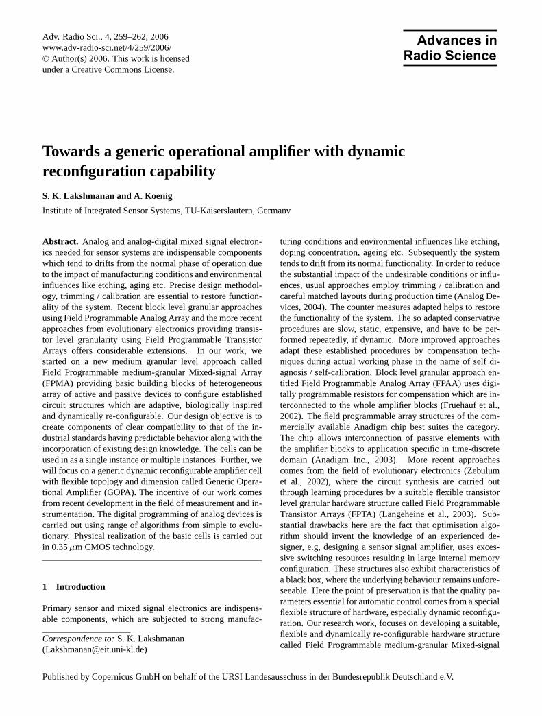
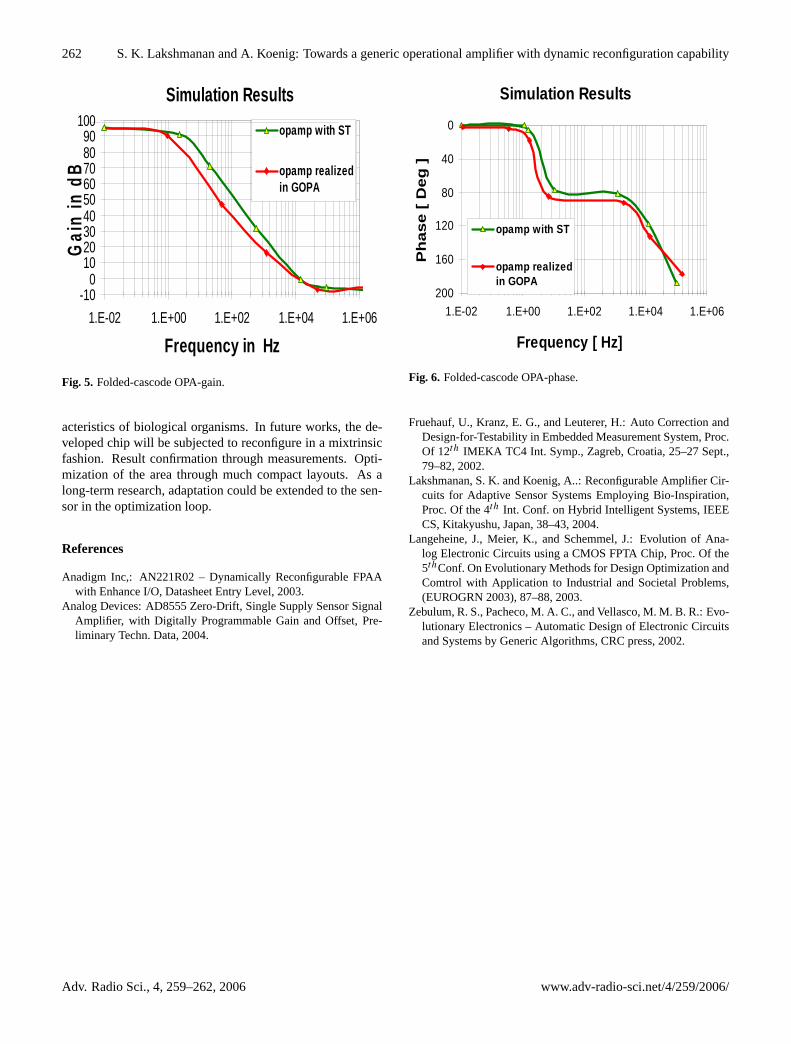
The layout consists a total of 45 scalable devices and59 topological switches. The performance curve of thefolded cascode operational amplifier is shown in Figs. 5 and 6for its gain and phase margin respectively. Different curvesin the graph shown in Figs. 5 and 6 refers to simulation re-sults obtained initially with ordinary transistors and later byreplacing with the scalable version. In this work, simulationswere carried out in the so called extrinsic fashion. A con-siderable degree of behavior comparability is to be expectedwith the manufactured chip of the dynamic re-configurablefolded cascode operational amplifier performed later with in-trinsic simulations. With regard to practical applications, inaddition to normal pins of the OpAmp, data (D) pin, enable(EN) pin, clock (clk) pin are essential. The enable signalensures that the digital section does not interact with opera-tion phase of the amplifier after suitable device selections areperformed. This ensures additional separation between thedifferent domains of analog and digital is not necessary. Theobjective of this chip comes after studying the need and ad-vancement in the field of measurement and instrumentation.Our design objective is to create cells of clear compatibilityto that of the industrial standards with expectable behavioralong with incorporation of existing design knowledge. Thechip can be used in as a single or multiple instances. Theprototype of the chip is under preparation.
5 Conclusion
In this paper, we have realized the implementation of the timecontinuous dynamically re-configurable sensor signal ampli-fier that is flexible in both topology and in sizing of the ac-tive and passive devices with drift compensation capabilities,compatible to that of the industrial standards. The flexibil-ity does not come for free. A compromising additional lay-out area is consumed. The chip under preparation will al-low implementation of algorithms ranging from a simple toOrganic / Evolutionary, exhibiting the desirable self-x char-
www.adv-radio-sci.net/4/259/2006/ Adv. Radio Sci., 4, 259–262, 2006
262 S. K. Lakshmanan and A. Koenig: Towards a generic operational amplifier with dynamic reconfiguration capability
Simulation Results
-100
102030405060708090
100
1.E-02 1.E+00 1.E+02 1.E+04 1.E+06
Frequency in Hz
Gai
n in
dB
opamp with ST
opamp realizedin GOPA
Simulation Results
0
40
80
120
160
2001.E-02 1.E+00 1.E+02 1.E+04 1.E+06
Frequency [ Hz]
Ph
ase
[ D
eg ]
opamp with ST
opamp realizedin GOPA
Figure 5. Folded-cascode OPA-gain Figure 6. Folded-cascode OPA-phase
The layout consists a total of 45 scalable devices and 59 topological switches. The
performance curve of the folded cascode operational amplifier is shown in Fig. 5 and Fig. 6
for its gain and phase margin respectively. Different curves in the graph shown in Fig .5 and
Fig. 6 refers to simulation results obtained initially with ordinary transistors and later by
replacing with the scalable version. In this work, simulations were carried out in the so called
extrinsic fashion. A considerable degree of behavior comparability is to be expected with the
manufactured chip of the dynamic re-configurable folded cascode operational amplifier
performed later with intrinsic simulations. With regard to practical applications, in addition to
normal pins of the OpAmp, data (D) pin, enable (EN) pin, clock (clk) pin are essential. The
enable signal ensures that the digital section does not interact with operation phase of the
amplifier after suitable device selections are performed. This ensures additional separation
between the different domains of analog and digital is not necessary. The objective of this
chip comes after studying the need and advancement in the field of measurement and
instrumentation. Our design objective is to create cells of clear compatibility to that of the
industrial standards with expectable behavior along with incorporation of existing design
knowledge. The chip can be used in as a single or multiple instances. The prototype of the
chip is under preparation.
7
Fig. 5. Folded-cascode OPA-gain.
acteristics of biological organisms. In future works, the de-veloped chip will be subjected to reconfigure in a mixtrinsicfashion. Result confirmation through measurements. Opti-mization of the area through much compact layouts. As along-term research, adaptation could be extended to the sen-sor in the optimization loop.
References
Anadigm Inc,: AN221R02 – Dynamically Reconfigurable FPAAwith Enhance I/O, Datasheet Entry Level, 2003.
Analog Devices: AD8555 Zero-Drift, Single Supply Sensor SignalAmplifier, with Digitally Programmable Gain and Offset, Pre-liminary Techn. Data, 2004.
Simulation Results
-100
102030405060708090
100
1.E-02 1.E+00 1.E+02 1.E+04 1.E+06
Frequency in Hz
Gai
n in
dB
opamp with ST
opamp realizedin GOPA
Simulation Results
0
40
80
120
160
2001.E-02 1.E+00 1.E+02 1.E+04 1.E+06
Frequency [ Hz]
Ph
ase
[ D
eg ]
opamp with ST
opamp realizedin GOPA
Figure 5. Folded-cascode OPA-gain Figure 6. Folded-cascode OPA-phase
The layout consists a total of 45 scalable devices and 59 topological switches. The
performance curve of the folded cascode operational amplifier is shown in Fig. 5 and Fig. 6
for its gain and phase margin respectively. Different curves in the graph shown in Fig .5 and
Fig. 6 refers to simulation results obtained initially with ordinary transistors and later by
replacing with the scalable version. In this work, simulations were carried out in the so called
extrinsic fashion. A considerable degree of behavior comparability is to be expected with the
manufactured chip of the dynamic re-configurable folded cascode operational amplifier
performed later with intrinsic simulations. With regard to practical applications, in addition to
normal pins of the OpAmp, data (D) pin, enable (EN) pin, clock (clk) pin are essential. The
enable signal ensures that the digital section does not interact with operation phase of the
amplifier after suitable device selections are performed. This ensures additional separation
between the different domains of analog and digital is not necessary. The objective of this
chip comes after studying the need and advancement in the field of measurement and
instrumentation. Our design objective is to create cells of clear compatibility to that of the
industrial standards with expectable behavior along with incorporation of existing design
knowledge. The chip can be used in as a single or multiple instances. The prototype of the
chip is under preparation.
7
Fig. 6. Folded-cascode OPA-phase.
Fruehauf, U., Kranz, E. G., and Leuterer, H.: Auto Correction andDesign-for-Testability in Embedded Measurement System, Proc.Of 12th IMEKA TC4 Int. Symp., Zagreb, Croatia, 25–27 Sept.,79–82, 2002.
Lakshmanan, S. K. and Koenig, A..: Reconfigurable Amplifier Cir-cuits for Adaptive Sensor Systems Employing Bio-Inspiration,Proc. Of the 4th Int. Conf. on Hybrid Intelligent Systems, IEEECS, Kitakyushu, Japan, 38–43, 2004.
Langeheine, J., Meier, K., and Schemmel, J.: Evolution of Ana-log Electronic Circuits using a CMOS FPTA Chip, Proc. Of the5thConf. On Evolutionary Methods for Design Optimization andComtrol with Application to Industrial and Societal Problems,(EUROGRN 2003), 87–88, 2003.
Zebulum, R. S., Pacheco, M. A. C., and Vellasco, M. M. B. R.: Evo-lutionary Electronics – Automatic Design of Electronic Circuitsand Systems by Generic Algorithms, CRC press, 2002.
Adv. Radio Sci., 4, 259–262, 2006 www.adv-radio-sci.net/4/259/2006/