rambus™ xdr™ clock generator - ti.com
TRANSCRIPT

www.ti.com
FEATURES
1
2
3
4
5
6
7
11
8
12
9
13
10
14
28
27
26
25
24
23
22
18
21
17
20
16
19
15
VDDP
VSSP
ISET
VSS
REFCLK
REFCLKB
VDDC
EN
VSSC
ID0
SCL
ID1
SDA
BYPASS
VDD
CLK0
CLK0B
VSS
CLK1
CLK1B
VDD
VSS
VSS
CLK3
CLK2
CLK3B
CLK2B
VDD
PW PACKAGE(TOP VIEW)
P0043-01
APPLICATIONS
DESCRIPTION
CDCD5704
SCAS823–DECEMBER 2006
Rambus™ XDR™ CLOCK GENERATOR
• High-Speed Clock Support: 300-MHz–667-MHzClock Source for XDR Memory Subsystemsand Redwood Logic Interface
• Quad (Open-Drain) Differential Output Drivers• Spread-Spectrum Compatible Clock Input Can
Be Distributed to Minimize EMI• Differential or Single-Ended Reference Clock
Input of 100 MHz or 133 MHz• Serial Interface Features: Programmable
Frequency Multiplier, Select Any One to FourOutputs and Mode of Operation
• Supports Frequency Multiplication Factors of:×3, ×4, ×5, ×6, ×8, ×9/2, ×15/2, ×15/4
• All PLL Loop Filter Components AreIntegrated
• Low |Cycle-to-Cycle| of 1–6 Cycle Jitter:– 40 ps: 300–635 MHz– 30 ps: 636–667 MHz
• PLLs Are Powered Down if No Valid REFClock (<10 MHz) Is Detected or VDD Is Below1.6 V
• Operates From Single 2.5-V Supply (±0.125 V)• Packaged in TSSOP-28• Commercial Temperature Range 0°C to 70°C
• XDR Memory Subsystem and Redwood LogicInterface
The CDCD5704 clock generator provides the necessary clock signals to support an XDR memory subsystemand Redwood logic interface using a reference clock input with or without spread-spectrum modulation.Contained in a 28-pin TSSOP package that includes four differential clock outputs, the CDCD5704 provides anoff-the-shelf solution for a broad range of high-performance interface applications.
The block diagram shows the major components of the CDCD5704, which include a phase-locked loop, abypass multiplexer, and four differential output buffers (CLK0 to CLK3). All four outputs can be disabled by alogical low at the input of the EN pin. An output is enabled when EN is high and a value of 1 is in its serialinterface register (RegA–RegD).
The PLL receives a reference clock input signal, REFCLK, and outputs a clock signal at a frequency equal to theinput frequency times the multiplication factor. The PLL output clock signal is fed to the differential output buffersto drive the enabled clocks. Disabled outputs are set to high impedance.
Please be aware that an important notice concerning availability, standard warranty, and use in critical applications of TexasInstruments semiconductor products and disclaimers thereto appears at the end of this data sheet.
Rambus, XDR are trademarks of Rambus Inc.All other trademarks are the property of their respective owners.
PRODUCTION DATA information is current as of publication date. Copyright © 2006, Texas Instruments IncorporatedProducts conform to specifications per the terms of the TexasInstruments standard warranty. Production processing does notnecessarily include testing of all parameters.

www.ti.com
B0137-01
REFCLK
BYPASS
CLK0
VSSP
VDDP VDDC VDD
VSSC VSS
VDD
VDDC
VDDP
CLK0B
CLK1
CLK1B
CLK2
CLK2B
CLK3
CLK3B
REFCLKB
MUX
CLK0
SDA
SCL
ID0
ID1
CLk1
CLK2
CLK3
EN
CLK0
Current and VoltageReference
ISET
RSET
PLL 1300 MHz to 667 MHz
PowerDownLogic
Serial InterfaceControl Logic
CDCD5704
SCAS823–DECEMBER 2006
The bypass mode routes the input clock REFCLK to the differential output buffers, bypassing the PLL.
To ensure that the CDCD5704 clock generator always performs correctly, the device switches off the PLL andthe outputs are in the high-impedance state, once the clock input is below 10 MHz. If the supply voltage VDD isless than VPUC, all logic gates are reset, the PLL is powered down, and the outputs are in the high-impedancestate. Therefore, the device only starts its operation if these minimum requirements are met.
Because the CDCD5704 is based on PLL circuitry, it requires a stabilization time to achieve phase-lock of thePLL. With use of an external reference clock, this signal must be fixed-frequency and fixed-phase prior to thestart of stabilization time.
The device operates from a single 2.5-V supply voltage. The CDCD5704 device is characterized for operationfrom 0°C to 70°C.
FUNCTIONAL BLOCK DIAGRAM
2 Submit Documentation Feedback

www.ti.com
SERIAL INTERFACE
Serial Interface Operation Requirement
Serial Interface Device Address
CDCD5704
SCAS823–DECEMBER 2006
Table 1. TERMINAL FUNCTIONS
TERMINALTYPE DESCRIPTION
NAME NO.
BYPASS 14 Input If 0, the PLL is bypassed and the PLL is switched off.
CLK0 27 Output Output for Clock0
CLK0B 26 Output Complementary output for Clock0
CLK1 24 Output Output for Clock1
CLK1B 23 Output Complementary output for Clock1
CLK2 20 Output Output for Clock2
CLK2B 19 Output Complementary output for Clock2
CLK3 17 Output Output for Clock3
CLK3B 16 Output Complementary output for Clock3
EN 11 Input Output enable; if 0, all outputs are disabled.
ID0 12 Input Device ID, bit 0
ID1 13 Input Device ID, bit 1
ISET 3 Output Set clock driver current with external resistor
REFCLK 5 Input Reference clock input
REFCLKB 6 Input Complementary reference clock input
SCL 9 Input Serial interface clock, 3.3-V compatible
SDA 10 Input Serial interface data, 3.3-V compatible
VDD 15, 22, 28 Power 2.5-V power supply for outputs
VDDC 7 Power 2.5-V power supply for core
VDDP 1 Power 2.5-V power supply for PLL
VSS 4, 18, 21, 25 Ground Ground
VSSC 8 Ground Ground for core
VSSP 2 Ground Ground for PLL
The following section describes the serial interface programming. In general, the serial interface slave supportsbyte-write/-read and word-write/-read protocol as defined in the SMBus or I2C specification.
The internal timing of the serial interface logic block in the CDCD5704 requires a timing reference derived fromthe input clock (REFCLK). A reference clock must be present at the REFCLK pin for the serial interface to beoperational.
A6 A5 A4 A3 A2 A1 A0 W/R
1 1 0 1 1 ID1 ID0 0/1
The device-ID is determined by the external pins ID0 and ID1. They are part of the device 8-bit address.Therefore, four different devices (00, 01, 10, and 11) can be addressed via the same serial interface. The leastsignificant bit of the address designates a write or read operation.
R/W Bit:0 = write to CDCD5704 device1 = read from CDCD5704 device
3Submit Documentation Feedback
www.ti.com
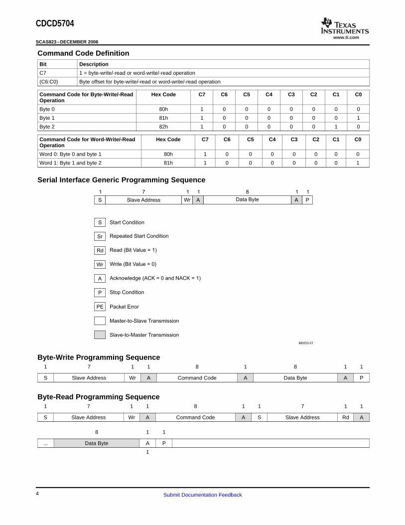
Command Code Definition
Serial Interface Generic Programming Sequence
M0053-01
1 7 1 1 8 1 1
S
S
Slave Address Wr A Data Byte A P
Start Condition
Sr Repeated Start Condition
Rd Read (Bit Value = 1)
Wr Write (Bit Value = 0)
A Acknowledge (ACK = 0 and NACK = 1)
P Stop Condition
PE Packet Error
Master-to-Slave Transmission
Slave-to-Master Transmission
Byte-Write Programming Sequence
Byte-Read Programming Sequence
CDCD5704
SCAS823–DECEMBER 2006
Bit Description
C7 1 = byte-write/-read or word-write/-read operation
(C6:C0) Byte offset for byte-write/-read or word-write/-read operation
Command Code for Byte-Write/-Read Hex Code C7 C6 C5 C4 C3 C2 C1 C0Operation
Byte 0 80h 1 0 0 0 0 0 0 0
Byte 1 81h 1 0 0 0 0 0 0 1
Byte 2 82h 1 0 0 0 0 0 1 0
Command Code for Word-Write/-Read Hex Code C7 C6 C5 C4 C3 C2 C1 C0Operation
Word 0: Byte 0 and byte 1 80h 1 0 0 0 0 0 0 0
Word 1: Byte 1 and byte 2 81h 1 0 0 0 0 0 0 1
1 7 1 1 8 1 8 1 1
S Slave Address Wr A Command Code A Data Byte A P
1 7 1 1 8 1 1 7 1 1
S Slave Address Wr A Command Code A S Slave Address Rd A
8 1 1
... Data Byte A P
1
4 Submit Documentation Feedback

www.ti.com
Word-Write Programming Sequence
Word-Read Programming Sequence
T0131-01
P S P
t(BUS)
tw(SCLL) tw(SCLH)
tr(SM) tf(SM)
th(START)
tsu(SDATA)
th(SDATA)
tsu(STOP)tsu(START)
tr(SDATA)tf(SDATA)
SCLK
SDATA
VIH(SM)
VIH(SM)
VIL(SM)
VIL(SM)
ABit 7 (MSB) Bit 6 Bit 0 (LSB)
CDCD5704
SCAS823–DECEMBER 2006
1 7 1 1 8 1 8 1
S Slave Address Wr A Command Code A Data Byte Low A
8 1 1
... Data Byte High A P
1 7 1 1 8 1 1 7 1 1
S Slave Address Wr A Command Code A S Slave Address Rd A
8 1 8 1 1
... Data Byte A Data Byte A P
1
Figure 1. Timing Diagram, Serial Control Interface
5Submit Documentation Feedback

www.ti.com
Serial Interface Configuration Command Bitmap
Byte 0
Byte 1
Byte 2
CDCD5704
SCAS823–DECEMBER 2006
Bit Bit Name Description/Function Type Power-Up Condition
7 RES Reserved R/W 0
6 MULT2 Multiplication factor, bit 2 R/W 0
5 MULT1 Multiplication factor, bit 1 R/W 0
4 MULT0 Multiplication factor, bit 0 R/W 1
3 RegA Enable CLK0 R/W 1
2 RegB Enable CLK1 R/W 1
1 RegC Enable CLK2 R/W 1
0 RegD Enable CLK3 R/W 1
Bit Bit Name Description/Function Type Power-Up Condition
7 RES Reserved R/W 0
6 RES Reserved R/W 0
5 RES Reserved R/W 0
4 RES Reserved R/W 0
3 RES Reserved for vendor option R/W 0
2 RES Reserved for vendor option R/W 0
1 RES Reserved for vendor option R/W 0
0 RegTest Vendor test register. If high, then Vendor Test R/W 0
Bit Bit Name Description/Function Type Power-Up Condition
7 REV0 Device revision, bit 4 R 0
6 REV0 Device revision, bit 3 R 0
5 REV0 Device revision, bit 2 R 0
4 REV0 Device revision, bit 1 R 0
3 REV0 Device revision, bit 0 R 0
2 VID2 Vendor ID bit 2 R 0
1 VID1 Vendor ID bit 1 R 1
0 VID0 Vendor ID bit 0 R 1
6 Submit Documentation Feedback

www.ti.com
FUNCTIONAL DESCRIPTION OF THE LOGIC
PLL Multiplication Factor Selection
Modes of Operation
CDCD5704
SCAS823–DECEMBER 2006
Output Frequency (MHz)MultiplicationMult2 Mult1 Mult0 Factor REFCLK = 100 MHz REFCLK = 133 MHz
0 0 0 3 300 400
0 (1) 0 (1) 1 (1) 4 (1) 400 533
0 1 0 5 500 667
0 1 1 6 600 800 (2)
1 0 0 8 800 (2) – (2)
1 0 1 9/2 450 600
1 1 0 15/2 750 (2) – (2)
1 1 1 15/4 375 500
(1) Default settings after power up(2) Output at this frequency does not conform to all the ac device characteristics in the Device Characteristics table, or ouput frequency is
not supported.
EN BYPASS Reg-Test RegA RegB RegC RegD CLK0 CLK1 CLK2 CLK3
L X X X X X X HI-Z HI-Z HI-Z HI-Z
H X 1 X X X X RESERVED FOR VENDOR TEST
H L 0 X X X X REFCLK REFCLK REFCLK REFCLK
H H 0 0 0 0 0 HI-Z HI-Z HI-Z HI-Z
H H 0 1 0 0 0 PLL CLK HI-Z HI-Z HI-Z
H H 0 0 1 0 0 HI-Z PLL CLK HI-Z HI-Z
H H 0 1 1 0 0 PLL CLK PLL CLK HI-Z HI-Z
H H 0 0 0 1 0 HI-Z HI-Z PLL CLK HI-Z
H H 0 1 0 1 0 PLL CLK HI-Z PLL CLK HI-Z
H H 0 0 1 1 0 HI-Z PLL CLK PLL CLK HI-Z
H H 0 1 1 1 0 PLL CLK PLL CLK PLL CLK HI-Z
H H 0 0 0 0 1 HI-Z HI-Z HI-Z PLL CLK
H H 0 1 0 0 1 PLL CLK HI-Z HI-Z PLL CLK
H H 0 0 1 0 1 HI-Z PLL CLK HI-Z PLL CLK
H H 0 1 1 0 1 PLL CLK PLL CLK HI-Z PLL CLK
H H 0 0 0 1 1 HI-Z HI-Z PLL CLK PLL CLK
H H 0 1 0 1 1 PLL CLK HI-Z PLL CLK PLL CLK
H H 0 0 1 1 1 HI-Z PLL CLK PLL CLK PLL CLK
H H 0 (1) 1 (1) 1 (1) 1 (1) 1 (1) PLL CLK PLL CLK PLL CLK PLL CLK
(1) Default settings after power up
7Submit Documentation Feedback

www.ti.com
ABSOLUTE MAXIMUM RATINGS
RECOMMENDED DC OPERATING CONDITIONS
CDCD5704
SCAS823–DECEMBER 2006
over operating free-air temperature range (unless otherwise noted) (1)
VALUE UNIT
VDD Supply voltage range –0.3 to 2.8 V
For SCL and SDA –0.3 to 3.6VI Input voltage range (2) V
For all other inputs –0.3 to VDD + 0.25
VO Output voltage range (2) –0.5 to VDD + 0.5 V
IIK Input clamp current, (VI < 0, VI > VDD) ±20 mA
IO Continuous output current ±50 mA
No airflow 94.4
Airflow 150 ft/min 82.8RθJA Thermal resistance, junction-to-ambient (3) K/W
Airflow 250 ft/min 79.1
Airflow 500 ft/min 74
RθJC Thermal resistance, junction-to-case (3) No airflow 31.8 K/W
RθJB Thermal resistance, junction-to-board (3) No airflow 68.9 K/W
TJ Maximum junction temperature 125 °C
Tstg Storage temperature range –65 to 150 °C
(1) Stresses beyond those listed under absolute maximum ratings may cause permanent damage to the device. These are stress ratingsonly, and functional operation of the device at these or any other conditions beyond those indicated under recommended operatingconditions is not implied. Exposure to absolute-maximum-rated conditions for extended periods may affect device reliability.
(2) The input and output negative voltage ratings may be exceeded if the input and output clamp-current ratings are observed.(3) The package thermal impedance is calculated in accordance with JESD 51 and JEDEC2S1P (high-k board).
MIN NOM MAX UNIT
VDDP Supply voltage for PLL 2.375 2.5 2.625 V
VDDC Supply voltage for core 2.375 2.5 2.625 V
VDD Supply voltage for clock buffers 2.375 2.5 2.625 V
TA Operating free-air temperature 0 70 °C
VIL,CLK Low-level input voltage, REFCLK/REFCLKB –0.15 0.15 V
VIX,CLK Crossing-point voltage, input voltage threshold, REFCLK/REFCLKB 0.2 0.55 V
VIH,CLKD High-level input voltage, REFCLK/REFCLKB 0.6 0.95 V
∆VIX,CLK Difference in crossing-point voltage 0.15 V
VIL SE Low-level, single-ended input voltage, REFCLK –0.15 Vth SE – 0.3 V
Vth SE Single-ended input-voltage threshold, REFCLK (1) 0.35 0.5 VDD V
VIH SE High-level, single-ended input voltage, REFCLK Vth SE + 0.3 2.625 V
VIL L Low-level input voltage, ID0, ID1, EN, BYPASS –0.15 0.8 V
VIH L High-level input voltage, ID0, ID1, EN, BYPASS 1.4 2.625 V
VIL SM Low-level input voltage, SCL, SDA (2) –0.15 0.8 V
VIH SM High-level input voltage, SCL, SDA (2) 1.4 3.465 V
(1) When using a single-ended clock input, Vth is supplied to the REFCLKB pin. Duty cycle of single-ended REFCLK input is measured atVth.
(2) This range of SCL and SDA input high voltage allows the CDCD5704 to co-exist with 3.3 V, 2.5 V, and 1.8 V devices on the sameserial-interface bus system.
8 Submit Documentation Feedback
www.ti.com
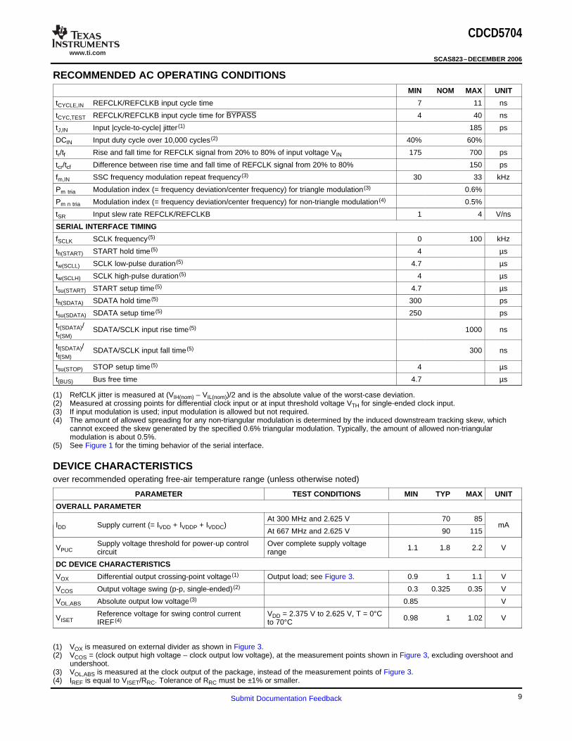
RECOMMENDED AC OPERATING CONDITIONS
DEVICE CHARACTERISTICS
CDCD5704
SCAS823–DECEMBER 2006
MIN NOM MAX UNIT
tCYCLE,IN REFCLK/REFCLKB input cycle time 7 11 ns
tCYC,TEST REFCLK/REFCLKB input cycle time for BYPASS 4 40 ns
tJ,IN Input |cycle-to-cycle| jitter (1) 185 ps
DCIN Input duty cycle over 10,000 cycles (2) 40% 60%
tr/tf Rise and fall time for REFCLK signal from 20% to 80% of input voltage VIN 175 700 ps
tcr/tcf Difference between rise time and fall time of REFCLK signal from 20% to 80% 150 ps
fm,IN SSC frequency modulation repeat frequency (3) 30 33 kHz
Pm tria Modulation index (= frequency deviation/center frequency) for triangle modulation (3) 0.6%
Pm n tria Modulation index (= frequency deviation/center frequency) for non-triangle modulation (4) 0.5%
tSR Input slew rate REFCLK/REFCLKB 1 4 V/ns
SERIAL INTERFACE TIMING
fSCLK SCLK frequency (5) 0 100 kHz
th(START) START hold time (5) 4 µs
tw(SCLL) SCLK low-pulse duration (5) 4.7 µs
tw(SCLH) SCLK high-pulse duration (5) 4 µs
tsu(START) START setup time (5) 4.7 µs
th(SDATA) SDATA hold time (5) 300 ps
tsu(SDATA) SDATA setup time (5) 250 ps
tr(SDATA)/ SDATA/SCLK input rise time (5) 1000 nstr(SM)
tf(SDATA)/ SDATA/SCLK input fall time (5) 300 nstf(SM)
tsu(STOP) STOP setup time (5) 4 µs
t(BUS) Bus free time 4.7 µs
(1) RefCLK jitter is measured at (VIH(nom) – VIL(nom))/2 and is the absolute value of the worst-case deviation.(2) Measured at crossing points for differential clock input or at input threshold voltage VTH for single-ended clock input.(3) If input modulation is used; input modulation is allowed but not required.(4) The amount of allowed spreading for any non-triangular modulation is determined by the induced downstream tracking skew, which
cannot exceed the skew generated by the specified 0.6% triangular modulation. Typically, the amount of allowed non-triangularmodulation is about 0.5%.
(5) See Figure 1 for the timing behavior of the serial interface.
over recommended operating free-air temperature range (unless otherwise noted)
PARAMETER TEST CONDITIONS MIN TYP MAX UNIT
OVERALL PARAMETER
At 300 MHz and 2.625 V 70 85IDD Supply current (= IVDD + IVDDP + IVDDC) mA
At 667 MHz and 2.625 V 90 115
Supply voltage threshold for power-up control Over complete supply voltageVPUC 1.1 1.8 2.2 Vcircuit range
DC DEVICE CHARACTERISTICS
VOX Differential output crossing-point voltage (1) Output load; see Figure 3. 0.9 1 1.1 V
VCOS Output voltage swing (p-p, single-ended) (2) 0.3 0.325 0.35 V
VOL,ABS Absolute output low voltage (3) 0.85 V
Reference voltage for swing control current VDD = 2.375 V to 2.625 V, T = 0°CVISET 0.98 1 1.02 VIREF (4) to 70°C
(1) VOX is measured on external divider as shown in Figure 3.(2) VCOS = (clock output high voltage – clock output low voltage), at the measurement points shown in Figure 3, excluding overshoot and
undershoot.(3) VOL,ABS is measured at the clock output of the package, instead of the measurement points of Figure 3.(4) IREF is equal to VISET/RRC. Tolerance of RRC must be ±1% or smaller.
9Submit Documentation Feedback
www.ti.com
CDCD5704
SCAS823–DECEMBER 2006
DEVICE CHARACTERISTICS (continued)over recommended operating free-air temperature range (unless otherwise noted)
PARAMETER TEST CONDITIONS MIN TYP MAX UNIT
IOL/IREF Ratio of output low current to reference current 6.8 7 7.2
IOL,ABS Minimum current at VOL,ABS(5) VOL,ABS = 0.85 V 45 mA
VDD = 2.375 V to 2.625 V,VOL,SDA SDA output low voltage 0.4 VIOH = 4 mA
VDD = 2.375 V to 2.625 V,IOL,SDA SDA output low current 6 mAVO = 0.8 V
IOZ Output 3-state current CLK0 to CLK4 ±50 µA
IIR REFCLK input current VI = 0 V or VDD ±5 µA
IIL Logic input current VI = 0 V or VDD ±10 µA
AC DEVICE CHARACTERISTICS
Input capacitance, REFCLK,CIR 2 7 pFREFCLKB (6)
CIL Input capacitance logic pins (7) 2 10 pF
300 MHz to 667 MHz, possibletCYCLE Clock cycle time (8) 1.5 3.33 nsSSC is not taken into account
10,000 cycles, 300 MHz 40to 635 MHz (9)
tjit(per) |Cycle-to-cycle jitter| of 1–6 clock cycles ps10,000 cycles, 636 MHz 30to 667 MHz (9)
L1 SSB phase noise at 1 MHz 300-MHz–667-MHz output (10) –115 –97 dBc/Hz
L20 SSB phase noise at 20 MHz 300-MHz–667-MHz output (10) –150 –128 dBc/Hz
VDD = 2.375 V to 2.625 V,∆tskew(o) Drift in tskew(o)(11) 15 psT = 0 to 70°C
odc Output duty cycle 45% 50% 55%
300 MHz to 635 MHz 40tODC,ERR |Cycle-to-cycle| duty-cycle error ps
636 MHz to 667 MHz 30
tERR,SSC PLL output phase error when tracking SSC –100 100 ps
tr/tf Output rise and fall time VOUT = 20%–80% 100 300 ps
VOUT = 20%–80%, fout = 300 MHztcr/tcf Difference between output rise and fall times 100 psto 667 MHz
ZOUT Output dynamic impedance (12) VOL = 0.9 V 750 Ω
Time from VDD, VDDP, VDDCtL Power-up lock time being applied and settled until 3 ms
clock outputs are settled
PLL lock time after (1) frequency change via Time from signals for selecting aserial interface (programming of SCL and SDA mode of operation (1) or (2)tL(ω) 3 mspins completed) or (2) EN and/or BYPASS applied and settled until clockchanged state outputs are settled
(5) Minimum IOL,ABS is measured at the clock output pins of the package, as shown in Figure 3.(6) Capacitance measured at frequency = 1 MHz, dc bias = 0.9 V, and VAC < 100 mV(7) Capacitance measured at frequency = 1 MHz, dc bias = 0.9 V, and VAC < 100 mV(8) Maximum and minimum output clock cycle times are based on nominal output frequency of 300 MHz and 667 MHz, respectively. For
spread-spectrum-modulated differential or single-ended REFCLK, the output clock tracks the modulation of the input.(9) Output short-term jitter specification is the absolute value of the worst-case deviation and is defined in the Jitter section.(10) Device must not exceed the upper limit of L(f) for 1-MHz to 100-MHz offset as shown in the Phase Noise section.(11) tskew is the timing difference between any two of the four differential clocks and is measured at common-mode voltage. ∆tskew is the
change in tskew when the operating temperature and supply voltage change.(12) ZOUT is defined at the output pins directly. The value is determined as the ac small-signal impedance at low frequencies (< 100 kHz)
and when output is driving a high state.
10 Submit Documentation Feedback

www.ti.com
PHASE NOISE
−160
−150
−140
−130
−120
−110
−100
−90
−80
fOffset − Offset Frequency − Hz
Pha
se N
oise
− d
Bc/
Hz
100k 1M 10M 100M20M
G001
Rambus Spec
667 MHz
Rambus Spec Range:1 MHz fOffset 20 MHz
300 MHz400 MHz
CDCD5704
SCAS823–DECEMBER 2006
For the offset frequency range from 1 MHz to 100 MHz, phase noise of the CDCD5704 does not exceed thesingle-sideband phase noise (spectral purity) described by the following equation given by Rambus.
L(f) = 10 log [1 + (50 × 106 / f)2.4] – 138 dBc/Hz
Selected numerical values are in given in the following table.
f = offset frequency 1 (L1) 5 10 15 20 (L20) 40 80 100 MHz
L(f) = SSB phase noise –97 –114 –121 –125 –128 –134 –137 –138 dBc/Hz
Figure 2. Phase Noise Plot
11Submit Documentation Feedback

www.ti.com
S0201-01
VTS
CLK
V = 1.2 VT
VTS
CLKB
V = 1.2 VT
XCG
CDCD5704IS
ET
Measurement Points
R1
R2
R3
R1
R2
R3
RT
RT
Z =500
W
Z =500
W
RRC
V(t)
tf tr
VH
VL
20%
80%
T0132-01
CDCD5704
SCAS823–DECEMBER 2006
NOTE: In the power-up sequence, the rise time for the external voltage applied to the clock output pins (VTS) must be equalto or longer than the rise time for the supply voltage of the device (VDD, VDDP, VDDC).
PARAMETER VALUE for 50-Ω LINE VALUE for IOL,ABS TOLERANCE UNIT
R1 Termination resistor 39.2 34 ±1% Ω
R2 Termination resistor 66.5 31.8 ±1% Ω
R3 Termination resistor 93.1 48.7 ±1% Ω
RT Termination resistor 49.9 28 ±1% Ω
RRC Swing control resistor 200 147 ±1% Ω
VTS Source termination voltage 2.5 2.5 ±5% V
VT Termination voltage 1.2 1.2 ±5% V
Figure 3. Output Test Load
Figure 4. Input and Output Waveforms
12 Submit Documentation Feedback

www.ti.com
T0133-01
Vx+
Vx, nom
Vx–
CLK
CLKB
T0134-01
CLK
tCYCLE,i
t = tJ CYCLE,i – t Over 10,000 Consecutive CyclesCYCLE,i+1
tCYCLE,i+1
CLKB
T0135-01
t4CYCLE,i t4CYCLE,i+1
t = tJ 4CYCLE,i – t Over 10,000 Consecutive Cycles4CYCLE,i+1
CLK
CLKB
T0136-01
t = tDC,ERR PW+,i – t andPW+,i+1 tPW–,i – tPW–,i+1
CLK
Cycle (i) Cycle (i+1)
CLKB
tPW–,i tPW–,i+1 tPW+,i+1
tCYCLE,i tCYCLE,i+1
tPW+,i
CDCD5704
SCAS823–DECEMBER 2006
Figure 5. Crossing-Point Voltage
Figure 6. One-Period Cycle-to-Cycle Jitter
Figure 7. Four-Period Cycle-to-Cycle Jitter
Figure 8. Cycle-to-Cycle Duty-Cycle Error
13Submit Documentation Feedback
www.ti.com
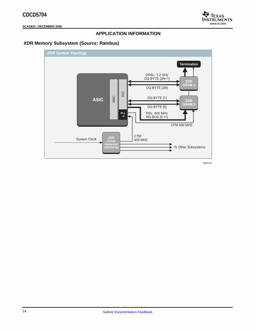
APPLICATION INFORMATION
XDR Memory Subsystem (Source: Rambus)
M0054-01
DRSL: 3.2 GHzDQ BYTE [2N+1]
DQ BYTE [2N]
DQ BYTE [1]
DQ BYTE [0]
·
·
·
CFM 400 MHZ
CTM400 MHZ
To Other Subsystems
System Clock
RSL: 800 MHzRQ BUS [0:11]
XDR System Topology
ASIC
PLL
4´
XM
C XIO
XDR
DRAM n
XDR
DRAM 0
XDR
Clock
Generator
CDCD5704
Termination
CDCD5704
SCAS823–DECEMBER 2006
14 Submit Documentation Feedback

PACKAGE OPTION ADDENDUM
www.ti.com 10-Dec-2020
Addendum-Page 1
PACKAGING INFORMATION
Orderable Device Status(1)
Package Type PackageDrawing
Pins PackageQty
Eco Plan(2)
Lead finish/Ball material
(6)
MSL Peak Temp(3)
Op Temp (°C) Device Marking(4/5)
Samples
CDCD5704PW ACTIVE TSSOP PW 28 50 RoHS & Green NIPDAU Level-1-260C-UNLIM 0 to 70 CDCD5704.
CDCD5704PWG4 ACTIVE TSSOP PW 28 50 RoHS & Green NIPDAU Level-1-260C-UNLIM 0 to 70 CDCD5704.
CDCD5704PWR ACTIVE TSSOP PW 28 2000 RoHS & Green NIPDAU Level-1-260C-UNLIM 0 to 70 CDCD5704.
CDCD5704PWRG4 ACTIVE TSSOP PW 28 2000 RoHS & Green NIPDAU Level-1-260C-UNLIM 0 to 70 CDCD5704.
(1) The marketing status values are defined as follows:ACTIVE: Product device recommended for new designs.LIFEBUY: TI has announced that the device will be discontinued, and a lifetime-buy period is in effect.NRND: Not recommended for new designs. Device is in production to support existing customers, but TI does not recommend using this part in a new design.PREVIEW: Device has been announced but is not in production. Samples may or may not be available.OBSOLETE: TI has discontinued the production of the device.
(2) RoHS: TI defines "RoHS" to mean semiconductor products that are compliant with the current EU RoHS requirements for all 10 RoHS substances, including the requirement that RoHS substancedo not exceed 0.1% by weight in homogeneous materials. Where designed to be soldered at high temperatures, "RoHS" products are suitable for use in specified lead-free processes. TI mayreference these types of products as "Pb-Free".RoHS Exempt: TI defines "RoHS Exempt" to mean products that contain lead but are compliant with EU RoHS pursuant to a specific EU RoHS exemption.Green: TI defines "Green" to mean the content of Chlorine (Cl) and Bromine (Br) based flame retardants meet JS709B low halogen requirements of <=1000ppm threshold. Antimony trioxide basedflame retardants must also meet the <=1000ppm threshold requirement.
(3) MSL, Peak Temp. - The Moisture Sensitivity Level rating according to the JEDEC industry standard classifications, and peak solder temperature.
(4) There may be additional marking, which relates to the logo, the lot trace code information, or the environmental category on the device.
(5) Multiple Device Markings will be inside parentheses. Only one Device Marking contained in parentheses and separated by a "~" will appear on a device. If a line is indented then it is a continuationof the previous line and the two combined represent the entire Device Marking for that device.
(6) Lead finish/Ball material - Orderable Devices may have multiple material finish options. Finish options are separated by a vertical ruled line. Lead finish/Ball material values may wrap to twolines if the finish value exceeds the maximum column width.
Important Information and Disclaimer:The information provided on this page represents TI's knowledge and belief as of the date that it is provided. TI bases its knowledge and belief on informationprovided by third parties, and makes no representation or warranty as to the accuracy of such information. Efforts are underway to better integrate information from third parties. TI has taken and

PACKAGE OPTION ADDENDUM
www.ti.com 10-Dec-2020
Addendum-Page 2
continues to take reasonable steps to provide representative and accurate information but may not have conducted destructive testing or chemical analysis on incoming materials and chemicals.TI and TI suppliers consider certain information to be proprietary, and thus CAS numbers and other limited information may not be available for release.
In no event shall TI's liability arising out of such information exceed the total purchase price of the TI part(s) at issue in this document sold by TI to Customer on an annual basis.

TAPE AND REEL INFORMATION
*All dimensions are nominal
Device PackageType
PackageDrawing
Pins SPQ ReelDiameter
(mm)
ReelWidth
W1 (mm)
A0(mm)
B0(mm)
K0(mm)
P1(mm)
W(mm)
Pin1Quadrant
CDCD5704PWR TSSOP PW 28 2000 330.0 16.4 6.9 10.2 1.8 12.0 16.0 Q1
PACKAGE MATERIALS INFORMATION
www.ti.com 17-Dec-2020
Pack Materials-Page 1

*All dimensions are nominal
Device Package Type Package Drawing Pins SPQ Length (mm) Width (mm) Height (mm)
CDCD5704PWR TSSOP PW 28 2000 853.0 449.0 35.0
PACKAGE MATERIALS INFORMATION
www.ti.com 17-Dec-2020
Pack Materials-Page 2


IMPORTANT NOTICE AND DISCLAIMER
TI PROVIDES TECHNICAL AND RELIABILITY DATA (INCLUDING DATASHEETS), DESIGN RESOURCES (INCLUDING REFERENCE DESIGNS), APPLICATION OR OTHER DESIGN ADVICE, WEB TOOLS, SAFETY INFORMATION, AND OTHER RESOURCES “AS IS” AND WITH ALL FAULTS, AND DISCLAIMS ALL WARRANTIES, EXPRESS AND IMPLIED, INCLUDING WITHOUT LIMITATION ANY IMPLIED WARRANTIES OF MERCHANTABILITY, FITNESS FOR A PARTICULAR PURPOSE OR NON-INFRINGEMENT OF THIRD PARTY INTELLECTUAL PROPERTY RIGHTS.These resources are intended for skilled developers designing with TI products. You are solely responsible for (1) selecting the appropriate TI products for your application, (2) designing, validating and testing your application, and (3) ensuring your application meets applicable standards, and any other safety, security, or other requirements. These resources are subject to change without notice. TI grants you permission to use these resources only for development of an application that uses the TI products described in the resource. Other reproduction and display of these resources is prohibited. No license is granted to any other TI intellectual property right or to any third party intellectual property right. TI disclaims responsibility for, and you will fully indemnify TI and its representatives against, any claims, damages, costs, losses, and liabilities arising out of your use of these resources.TI’s products are provided subject to TI’s Terms of Sale (www.ti.com/legal/termsofsale.html) or other applicable terms available either on ti.com or provided in conjunction with such TI products. TI’s provision of these resources does not expand or otherwise alter TI’s applicable warranties or warranty disclaimers for TI products.
Mailing Address: Texas Instruments, Post Office Box 655303, Dallas, Texas 75265Copyright © 2020, Texas Instruments Incorporated