ramp generator for adc built-in-self · pdf fileramp generator for adc built-in-self ... has a...
TRANSCRIPT
Ramp Generator for ADC Built-In-Self Test
Bruno Golzio Navarro Winkeler Raimundo Carlos Silvério Freire
[email protected] [email protected]
UFCG – Universidade Federal de Campina Grande NIMC – Núcleo de Instrumentação e Metrologia Científica
ABSTRACT This article aims to explain the development,
simulation and layout of a ramp generator, used in a
configuration of a ramp BIST. The test objects are the
analog-digital converters (ADC). The generator proposed
has a ramp with a calibrated slope. This characteristic
facilitates some error tests of converters. For this study we
used the platform Cadence® associated with the technology
XFAB 0.18 microns.
Keywords Ramp Generator, Analog-to-Digital Converter, BIST,
mixed-signal.
1. INTRODUCTION
A good part of the integrated circuits that are
manufactured today have analog capabilities in its
composition. The integration of highly complex analog
circuits is increasingly possible due to improved
manufacturing and treatment processes of silicon [1].
Nevertheless, the implementation of a large circuit also
promotes greater complexity for testing with the same. The
cost of testing an integrated circuit sometimes exceeds the
value of the design and manufacture of the circuit itself [2].
The test access for analog front-end and mixed-signal
interface (A/D and D/A converters) is limited. Therefore, it
is almost impossible to perform the test stimulus and
measurements outside the chip [1].
Because of the price growth in the testing of
integrated circuits, the use of BIST (built-in-self-test) has
increasingly been a great choice for error test. This choice
is due to evolution of technology, which promotes circuits
increasingly larger and more complex. A good set of BIST
methods have been developed to test integrated circuits
ADC. Among them we highlight: servo-loop method,
histogram method, oscillation BIST (OBIST) method [4]
and ramp BIST method [3].
Taking as an object of study the Ramp BIST method,
this article aims to explain, develop and test the circuit
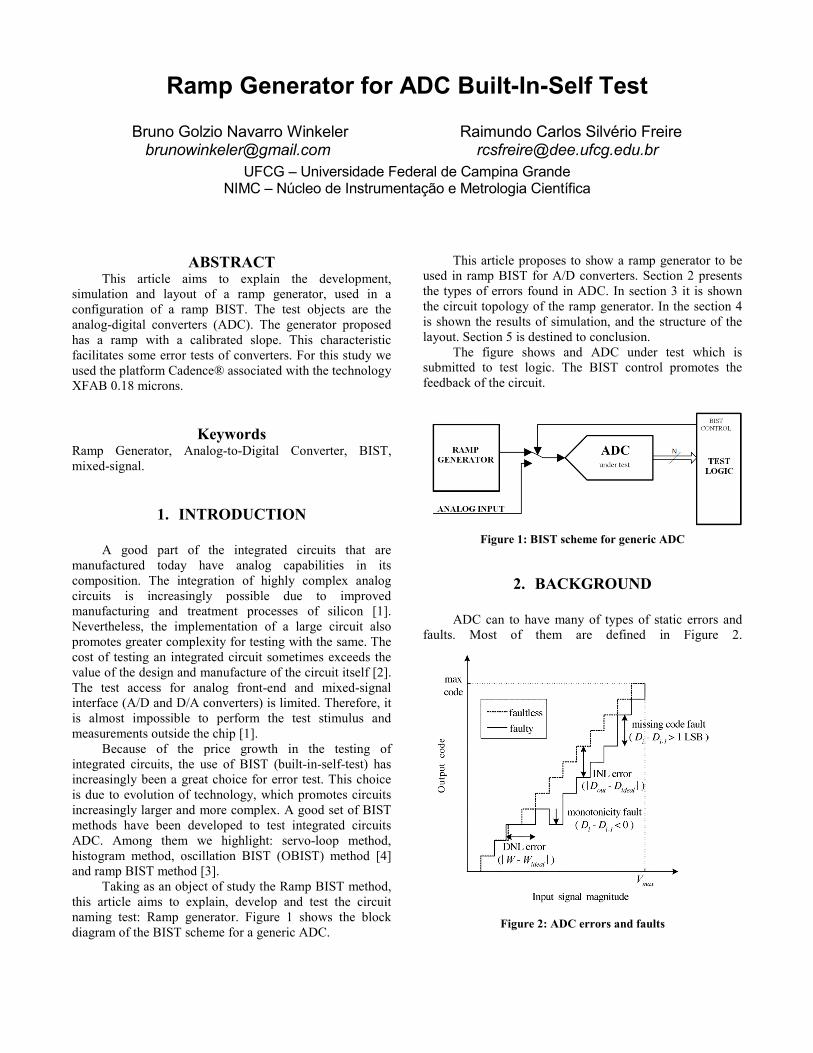
naming test: Ramp generator. Figure 1 shows the block
diagram of the BIST scheme for a generic ADC.
This article proposes to show a ramp generator to be
used in ramp BIST for A/D converters. Section 2 presents
the types of errors found in ADC. In section 3 it is shown
the circuit topology of the ramp generator. In the section 4
is shown the results of simulation, and the structure of the
layout. Section 5 is destined to conclusion.
The figure shows and ADC under test which is
submitted to test logic. The BIST control promotes the
feedback of the circuit.
Figure 1: BIST scheme for generic ADC
2. BACKGROUND
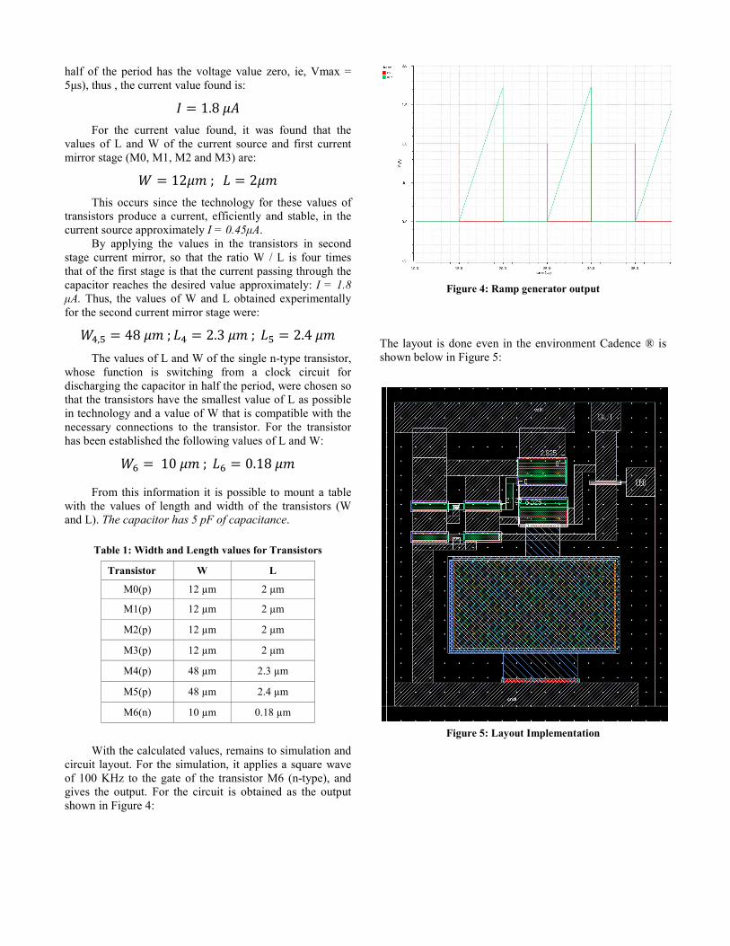
ADC can to have many of types of static errors and
faults. Most of them are defined in Figure 2.
Figure 2: ADC errors and faults

The non-linear errors of a ADC or DAC are
calculated in terms of least significant bits (LSB). The LSB
is the minimum voltage difference between consecutive
codes of an ADC or DAC ideal. A LSB can be defined as:
��� � �2� 1�
where V is the full range of the converter with N-bit
resolution.
When the difference current output of the ADC (Di)
with a previous output (Di-1) exceeds an LSB and the ramp
slope is sufficiently low has a missing code fault. Ramp to
an ever-increasing, has the conversion at some point
decreases, the ADC has a monotonocity fault. The INL
(integral nonlinearity) error is defined by the difference
between the ADC output (Dout) and the ideal expected
output (Dideal). The code width (W) is defined by the width
of the analog input that corresponds to 1-LSB digital
output. The difference between the measured code width
and the ideal code width (Wideal) is defined DNL
(deferential nonlinearity) error [3].
Applying a ramp to the input of ADC is possible,
through a logic test for the same ADC as shown in Figure
1, detecting errors and also to sort them according to the
above conditions. For this, however, it is necessary that the
ramp is perfectly calibrated and has a known frequency.
The proposed circuit achieved satisfactory results for both
conditions.
3. RAMP GENERATOR TOPOLOGY
To design a ramp generator is necessary to know the
frequency to work and have a device that has a linear
response to a constant excitation current, which in this case
is the capacitor. From equation 1 it is known that the
capacitor is an electric-device having at its terminals a
voltage given by:
� � � � ������
�� �0�2�
Having a constant current source can produce a linear
behavior of the voltage at the capacitor terminals. In other
words, to obtain a curve with a slope calibrated to apply a
current as constant as possible at the terminals of the
capacitor [5]. For the development of this conclusion is
necessary to design at the level of transistor, a source of
current with little variation of current. To this was used in
this article the topology shown in Figure 3. Has a cascode
current mirror to increase the loop current that charges the
capacitor.
Figure 3: Ramp Generator Circuit
The circuit shown has been made in this manner,
although there is a simpler configuration for same. This is
due to the need for a ramp calibrated for greater efficiency
test DNL and INL. Once the current mirror used should be
done so that the current to be as constant as possible.
4. RESULTS
Based on the topology of the ramp generator circuit,
the same has been assembled and simulated in Cadence ®
environment. The choice of values of length (W) and width
(L) of transistors was defined by the selection of some
fixed parameters of the circuit, such as operating frequency
and capacitance of the capacitor. The maximum voltage
value is 1.8 volts. It occurs due to technology and
fabrication process. Was chosen for this topology
capacitance of 5 pF, which in the course of circuit
integration represents a considerable size of the capacitor.
The frequency was chosen to be 100 KHz. The choice of
this specific frequency to ensure sampling from the ADC
efficiently.
From the parameters considered, knowing that it must
have a constant current, and equation 2 is that:
�� � � 1� �. � ���
�� �0�3�
Considering v(0) = 0, ie, the capacitor is initially
discharged, we have:
�� � � 1� . �. 4� Then for C = 5pF and knowing that VC (5 µs) = 1.8 V
(the topology of the ramp 100 Khz is constructed such that
half of the period has the voltage value zero, ie, Vmax =
5µs), thus , the current value found is:
� � 1.8��
For the current value found, it was found that the
values of L and W of the current source and first current
mirror stage (M0, M1, M2 and M3) are:
� � 12� ; � � 2�
This occurs since the technology for these values of
transistors produce a current, efficiently and stable, in the
current source approximately I = 0.45µA.
By applying the values in the transistors in second
stage current mirror, so that the ratio W / L is four times
that of the first stage is that the current passing through the
capacitor reaches the desired value approximately: I = 1.8
µA. Thus, the values of W and L obtained experimentally
for the second current mirror stage were:
�",$ � 48� ; �" � 2.3� ; �$ � 2.4�
The values of L and W of the single n-type transistor,
whose function is switching from a clock circuit for
discharging the capacitor in half the period, were chosen so
that the transistors have the smallest value of L as possible
in technology and a value of W that is compatible with the
necessary connections to the transistor. For the transistor
has been established the following values of L and W:
�% � 10� ; �% � 0.18�
From this information it is possible to mount a table
with the values of length and width of the transistors (W
and L). The capacitor has 5 pF of capacitance.
Table 1: Width and Length values for Transistors
Transistor W L
M0(p) 12 µm 2 µm
M1(p) 12 µm 2 µm
M2(p) 12 µm 2 µm
M3(p) 12 µm 2 µm
M4(p) 48 µm 2.3 µm
M5(p) 48 µm 2.4 µm
M6(n) 10 µm 0.18 µm
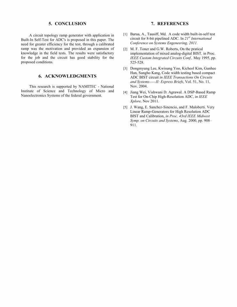
With the calculated values, remains to simulation and
circuit layout. For the simulation, it applies a square wave
of 100 KHz to the gate of the transistor M6 (n-type), and
gives the output. For the circuit is obtained as the output
shown in Figure 4:
Figure 4: Ramp generator output
The layout is done even in the environment Cadence ® is
shown below in Figure 5:
Figure 5: Layout Implementation
5. CONCLUSION
A circuit topology ramp generator with application in
Built-In Self-Test for ADC's is proposed in this paper. The
need for greater efficiency for the test, through a calibrated
ramp was the motivation and provided an expansion of
knowledge in the field tests. The results were satisfactory
for the job and the circuit has good stability for the
proposed conditions.
6. ACKNOWLEDGMENTS
This research is supported by NAMITEC - National
Institute of Science and Technology of Micro and
Nanoelectronics Systems of the federal government.
7. REFERENCES
[1] Barua, A., Tausiff, Md. A code width built-in-self test
circuit for 8-bit pipelined ADC. In 21st International
Conference on Systems Engeneering, 2011.
[2] M. F. Toner and G.W. Roberts, On the pratical
implementation of mixed analog-digital BIST, in Proc.
IEEE Custom Integrated Circuits Conf., May 1995, pp.
525-528.
[3] Dongmyung Lee, Kwisung Yoo, Kicheol Kim, Gunhee
Han, Sungho Kang, Code width testing based compact
ADC BIST circuit in IEEE Transactions On Circuits
and Systems-----II: Express Briefs, Vol. 51, No. 11,
Nov. 2004.
[4] Jiang Wei, Vishwani D. Agrawal. A DSP-Based Ramp
Test for On-Chip High-Resolution ADC, in IEEE
Xplore, Nov 2011.
[5] J. Wang, E. Sanchez-Sinencio, and F. Maloberti. Very
Linear Ramp-Generators for High Resolution ADC
BIST and Calibration, in Proc. 43rd IEEE Midwest
Symp. on Circuits and Systems, Aug. 2000, pp. 908–
911.