random access scan - ee.iitb.ac.inviren/courses/2012/ee709/lecture22.pdfautomatic scan insertion in...
TRANSCRIPT

Random Access Scan
Virendra Singh Associate Professor
Computer Architecture and Dependable Systems Lab
Dept. of Electrical Engineering
Indian Institute of Technology Bombay [email protected]
EE 709: Testing & Verification of VLSI Circuits
Lecture – 22 (Feb 16, 2012)

Scan Overheads • IO pins: One pin necessary.
• Area overhead:
– Gate overhead = [4 nsff/(ng+10nff)] x 100%, where ng = comb. gates; nff = flip-flops; Example – ng = 100k gates, nff = 2k flip-flops, overhead = 6.7%.
– More accurate estimate must consider scan wiring and layout area.
• Performance overhead:
– Multiplexer delay added in combinational path; approx. two gate-delays.
– Flip-flop output loading due to one additional fanout; approx. 5-6%.
Feb 16, 2012 EE-709@IITB 2

Hierarchical Scan Scan flip-flops are chained within subnetworks
before chaining subnetworks.
Advantages:
Automatic scan insertion in netlist
Circuit hierarchy preserved – helps in debugging and design changes
Disadvantage: Non-optimum chip layout.
Feb 16, 2012 EE-709@IITB 3
SFF1
SFF2 SFF3
SFF4 SFF3 SFF1
SFF2 SFF4
Scanin Scanout
Scanin
Scanout
Hierarchical netlist Flat layout

Optimum Scan Layout
Feb 16, 2012 EE-709@IITB 4
IO
pad
Flip-
flop
cell
Interconnects
Routing
channels
SFF
cell
TC
SCANIN
SCAN
OUT
Y
X X’
Y’
Active areas: XY and X’Y’
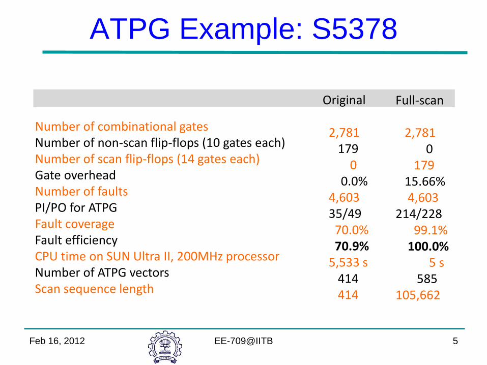
ATPG Example: S5378
Feb 16, 2012 EE-709@IITB 5
Original 2,781 179 0 0.0% 4,603 35/49 70.0% 70.9% 5,533 s 414 414
Full-scan 2,781 0 179 15.66% 4,603 214/228 99.1% 100.0% 5 s 585 105,662
Number of combinational gates Number of non-scan flip-flops (10 gates each) Number of scan flip-flops (14 gates each) Gate overhead Number of faults PI/PO for ATPG Fault coverage Fault efficiency CPU time on SUN Ultra II, 200MHz processor Number of ATPG vectors Scan sequence length

Scan Design Rules
Use only clocked D-type of flip-flops for all
state variables.
At least one PI pin must be available for test;
more pins, if available, can be used.
All clocks must be controlled from PIs.
Clocks must not feed data inputs of flip-flops.
Feb 16, 2012 EE-709@IITB 6

Correcting a Rule Violation
• All clocks must be controlled from PIs.
Feb 16, 2012 EE-709@IITB 7
Comb.
logic
Comb.
logic
D1
D2
CK
Q
FF
Comb.
logic
D1
D2
CK
Q
FF
Comb.
logic

Partial-Scan Definition A subset of flip-flops is scanned.
Objectives:
– Minimize area overhead and scan sequence length, yet achieve required fault coverage
– Exclude selected flip-flops from scan:
Improve performance
Allow limited scan design rule violations
– Allow automation:
In scan flip-flop selection
In test generation
– Shorter scan sequences
Feb 16, 2012 EE-709@IITB 8

Partial-Scan Architecture
Feb 16, 2012 EE-709@IITB
9
FF
FF
SFF
SFF
Combinational circuit
PI PO
CK1
CK2 SCANOUT
SCANIN
TC

Relevant Results
Theorem1: A cycle-free circuit is always initializable. It is also initializable in the presence of any non-flip-flop fault.
Theorem 2: Any non-flip-flop fault in a cycle-free circuit can be detected by at most dseq + 1 vectors.
ATPG complexity: To determine that a fault is untestable in a cyclic circuit, an ATPG program using nine-valued logic may have to analyze 9Nff time-frames, where Nff is the number of flip-flops in the circuit.
Feb 16, 2012 EE-709@IITB 10

A Partial-Scan Method
Select a minimal set of flip-flops for scan to
eliminate all cycles.
Alternatively, to keep the overhead low only long
cycles may be eliminated.
In some circuits with a large number of self-loops,
all cycles other than self-loops may be eliminated.
Feb 16, 2012 EE-709@IITB 11

The MFVS Problem For a directed graph find a set of vertices with smallest
cardinality such that the deletion of this vertex-set makes the graph acyclic.
The minimum feedback vertex set (MFVS) problem is NP-complete; practical solutions use heuristics.
A secondary objective of minimizing the depth of acyclic graph is useful.
Feb 16, 2012 EE-709@IITB 12
1 2
3
4 5 6
L=3
1 2
3
4 5 6 L=2
L=1
s-graph A 6-flip-flop circuit

Should Serial Scan Continue
A solution to test power, test time and test data volume • Three Problems with serial-scan
– Test power
– Test application time
– Test data volume
• Efforts and limitations
– ATPG for low test power consumption
Test power Test length
– Reducing scan clock frequency
Test power Test application time
– Scan-chain re-ordering (with additional logic insertion)
Test power/time Design time
– Test Compression
Test time/data size Has limited capability for Compacted test
• Orthogonal attack
– Random access scan instead of Serial-scan
– Hardware overhead? Silicon cost << Testing cost
Feb 16, 2012 EE-709@IITB 13

Random Access Scan
Architecture
Each FF has unique address
Address shift register
X-Y Decoder
Select FF to write/read
Feb 16, 2012 EE-709@IITB 14
Saluja et al [ITC’04]
A solution to test power, test time and test data volume

Scan Operation Example
• Test vector
Test PPI(ii)
PPO(oi)
t1 00101 00110
t2 00100 00101
t3 11010 11010
t4 00111 01011
Feb 16, 2012 EE-709@IITB 15
Scan operation for t2
CUT0
0
1
1
t1
0
0
0
1
01
1
0
1
1
i1 o1CUT
0
0
1
0
t2
0
0
0
1
10
1
0
1
1
i2 o2
Scan-in
operation
i1
o1
i2
o2
i3
o3
i4
o4
1
No. of scan
5 45
Complete test application
Total number of scan operation = 15
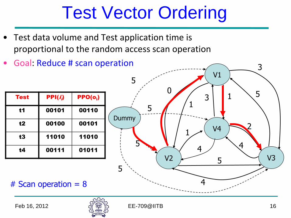
Test Vector Ordering
• Test data volume and Test application time is proportional to the random access scan operation
• Goal: Reduce # scan operation
Test PPI(i
i)
PPO(oi)
t1 00101 00110
t2 00100 00101
t3 11010 11010
t4 00111 01011
Feb 16, 2012 EE-709@IITB 16
V3
Dummy
V2
V4
V1 5
5
5
5
0 1
1 3
3
5
4
2
4
5
1
4
# Scan operation = 8

Hamming Distance Reduction
• Don’t care values in PPI do not need scan operation
– Use Don’t care identification method
Fully specified test vector Vectors w/ X values on targeted bit positions
without loss of fault coverage
1. Before vector ordering: Identify don’t cares in PPI
2. Vector ordering
3. Simulate test vector in order / Fill X’s with previous vectors PPO
4. Identify more X’s on targeted bit in PPI
- odd vector
- even vector
5. Repeat 3,4 until no more X’s are identified
Feb 16, 2012 EE-709@IITB 17
C
U
T
TF1
C
U
T
TF2
C
U
T
TF3
C
U
T
TF4
1
X
1
0
X
0
X
1
X
0
X
1
1
0
X
1
X
0
0
1
1
X
1
1
0
1
X
0
1
1
1
1
0
1
1
1
0
0
X
0
0
X
1
1
0
1
1
0
1
1
1
1
1
0
1
1
1
0
X
1
1
1
0
0
1
Targeted
Change allowed
X 1 0
1
1

Optimizing Address Scan • The cost of address shifting
– # of scan operation x ASR width – Example address set = { 1, 5, 6, 11 } for 4-bit ASR – 4 X 4 = 16
• Proper ordering of address can minimize shifting cost – Apply 11(1011) after 5(0101) needs only 1 left-shift
• Minimizing address shifting cost – Construct Address Shifting Distance Graph (ASD-graph) – Find min-cost Hamiltonian path using ATSP algorithm ( Result : 5 shifts )
Feb 16, 2012 EE-709@IITB 18
0001
0110
1011
2
0101
4 24
3
3
1
2
2
4
1
3
V = Aij = {1,5,6,11}
G = < V, E >
w(eij) =
0000
1
4
3
3
The number of minimum left-shift operation for the transition from v
i to v
j.
E = {eij | eij is an edge between vi and vj}
Last ASR contents of prev ious test vector

Result (Test Time/Data)
Feb 16, 2012 EE-709@IITB 19
Test data volume
K
100K
200K
300K
400K
500K
600K
700K
800K
900K
1000K
s132
07
s158
50
s359
32
s384
17
s385
84
b17s
b20s
b22s
Benchmarks
Bits
Serial
RAS
Test Application time
K
100K
200K
300K
400K
500K
600K
700K
800K
900K
1000K
s132
07
s158
50
s359
32
s384
17
s385
84
b17s
b20s
b22s
Benchmarks
Clo
cks
Serial
RAS

Thank You
Feb 16, 2012 EE-709@IITB 20