randomization of gold nano-brick arrays: a tool for sers ... · randomization of gold nano-brick...
TRANSCRIPT

Randomization of gold nano-brickarrays: a tool for SERS enhancement
Yoshiaki Nishijima,1,∗ Jacob B. Khurgin,2 Lorenzo Rosa,3,4
Hideki Fujiwara,5 Saulius Juodkazis3,4
1 Department of Electrical and Computer Engineering, Graduate School of Engineering,Yokohama National University, 79-5 Tokiwadai, Hodogaya-ku, Yokohama 240-8501, Japan
2 Department of Electrical and Computer Engineering, Johns Hopkins University, Baltimore,MD 21218, USA
3 Centre for Micro-Photonics, Faculty of Engineering and Industrial Sciences, SwinburneUniversity of Technology, Hawthorn, VIC 3122, Australia
4 The Australian National Fabrication Facility – ANFF, Victoria node, Faculty of Engineeringand Industrial Sciences, Swinburne University of Technology, Hawthorn, VIC 3122, Australia
5 Research Institute for Electronic Science, Hokkaido University, Sapporo 001-0020, Japan∗[email protected]
Abstract: Surface enhanced Raman scattering (SERS) was measured onperiodic and randomly arranged patterns of Au nano-bricks (rectangularparallelepipeds). Resonant SERS conditions were investigated of a near-IRdye deposited on nanoparticles. Random mixtures of Au nano-bricks withdifferent aspect ratio R showed stronger SERS enhancement as comparedto periodic patterns with constant aspect ratio (R varies from 1 to 4). SERSmapping revealed up to ∼ 4 times signal increase at the hot-spots. Experi-mental observation is verified by numerical modeling and is qualitativelyconsistent with generic scaling arguments of interaction between plasmonicnanoparticles. The effect of randomization on the polarization selectivityfor the transverse and longitudinal modes of nano-bricks is shown.
© 2013 Optical Society of America
OCIS codes: (160.4236) Nanomaterials; (240.6680) Surface plasmons; (250.5403) Plasmon-ics; (290.4210) Multiple scattering; (220.4241) Nanostructure fabrication; (310.6628) Sub-wavelength structures, nanostructures.
References and links1. J. Suh, C. Kim, W. Zhou, M. Huntington, D. Co, M. Wasielewski, and T. Odom, “Plasmonic bowtie nanolaser
arrays,” Nano Lett. 12, 5769–5774 (2012).2. W. Cai, A. P. Vasudev, and M. L. Brongersma, “Electrically controlled nonlinear generation of light with plas-
monics,” Science 333, 1720–1723 (2011).3. A. E. Miroshnichenko, S. Flach, and Y. S. Kivshar, “Fano resonances in nanoscale structures,” Rev. Mod.
Phys. 82, 2257–2298 (2010).4. A. Kabashin, P. Evans, S. Pastkovsky, W. Hendren, G. Wurtz, R. Atkinson, R. Pollard, V. Podolskiy, and A. Za-
yats, “Plasmonic nanorod metamaterials for biosensing,” Nat. Mater. 8, 867–871 (2009).5. T. Kondo, H. Masuda, and K. Nishio, “SERS in ordered array of geometrically controlled nanodots obtained
using anodic porous alumina,” J. Phys. Chem. C 117, 2531–2534 (2013).6. H.-X. Lin, J.-M. Li, B.-J. Liu, D.-Y. Liu, J. Liu, A. Terfort, Z.-X. Xie, Z.-Q. Tian, and B. Ren, “Uniform gold
spherical particles for single-particle surface-enhanced Raman spectroscopy,” Phys. Chem. Chem. Phys. 15,4130–4135 (2013).
7. S. Smitha, K. Gopchandran, N. Nair, K. Nampoothiri, and T. Ravindran, “SERS and antibacterial active greensynthesized gold nanoparticles,” Plasmonics 7, 515–524 (2012).
8. F. Lordan, J. H. Rice, B. Jose, R. J. Forster, and T. E. Keyes, “Site selective surface enhanced Raman on nanos-tructured cavities,” Appl. Phys. Lett. 99, 033104 (2011).
#187794 - $15.00 USDReceived 26 Mar 2013; revised 17 May 2013; accepted 19 May 2013; published 29 May 2013(C) 2013 OSA 3 June 2013 | Vol. 21, No. 11 | DOI:10.1364/OE.21.013502 | OPTICS EXPRESS 13502

9. K. Ueno, S. Juodkazis, M. Mino, V. Mizeikis, and H. Misawa, “Spectral sensitivity of uniform arrays of goldnanorods to the dielectric environment,” J. Phys. Chem. C 111, 4180–4184 (2007).
10. A. M. Michaels, M. Nirmal, and L. E. Brus, “Surface enhanced Raman spectroscopy of individual rhodamine 6Gmolecules on large Ag nanocrystals,” J. Am. Chem. Soc. 121, 9932–9939 (1999).
11. D. K. Gramotnev, A. Pors, M. Willatzen, and S. I. Bozhevolnyi, “Gap-plasmon nanoantennas and bowtie res-onators,” Phys. Rev. B 85, 045434 (2012).
12. J. Merlein, M. Kahl, A. Zuschlag, A. Sell, A. Halm, J. Boneberg, P. Leiderer, A. Leitenstorfer, and R. Brats-chitsch, “Nanomechanical control of an optical antenna,” Nat. Photonics 2, 230–233 (2008).
13. K. Ueno, S. Takabatake, K. Onishi, H. Itoh, Y. Nishijima, and H. Misawa, “Homogeneous nano-patterning usingplasmon-assisted photolithography,” Appl. Phys. Lett. 99, 011107 (2011).
14. W. Khunsin, B. Brian, J. Dorfmuller, M. Esslinger, R. Vogelgesang, C. Etrich, C. Rockstuhl, A. Dmitriev, andL. Lern, “Long-distance indirect excitation of nanoplasmonic resonances,” Nano Lett. 11, 2765–2769 (2011).
15. B. Lamprecht, G. Schider, R. T. Lechner, H. Ditlbacher, J. R. Krenn, A. Leitner, and F. R. Aussenegg, “Metalnanoparticle gratings: Influence of dipolar particle interaction on the plasmon resonance,” Phys. Rev. Lett. 84,4721–4724 (2000).
16. Y. Nishijima, L. Rosa, and S. Juodkazis, “Surface plasmon resonances in periodic and random patterns of goldnano-disks for broadband light harvesting,” Opt. Express 20, 11466–11477 (2012).
17. R.Buividas, L. Rosa, R. Sliupas, T. Kudrius, G. Slekys, V. Datsyuk, and S. Juodkazis, “Mechanism of fine rippleformation on surfaces of (semi)transparent materials via a half-wavelength cavity feedback,” Nanotechnology 22,055304 (2011).
18. A. Chou, E. Jaatinen, R. Buividas, G. Seniutinas, S. Juodkazis, E. L. Izake, and P. M. Fredericks, “SERS substratefor detection of explosives,” Nanoscale 4, 7419–7424 (2012).
19. A. K. Sarychev, V. A. Shubin, and V. M. Shalaev, “Anderson localization of surface plasmons and nonlinearoptics of metal-dielectric composites,” Phys. Rev. B 60, 16389–16408 (1999).
20. M. I. Stockman, S. V. Faleev, and S. J. Bergman, “Localization versus delocalization of surface plasmons innanosystems: can one state have both characteristics?,” Phys. Rev. Lett. 87, 167401 (2001).
21. J. B. Khurgin and G. Sun, “Impact of disorder on surface plasmons in two-dimensional arrays of metal nanopar-ticles,” Appl. Phys. Lett. 94, 22111 (2009).
22. D. J. Bergman and M. I. Stockman, “Surface plasmon amplification by stimulated emission of radiation: Quantumgeneration of coherent surface plasmons in nanosystems,” Phys. Rev. Lett. 90, 027402 (2003).
23. M. A. Noginov, G. Zhu, A. M. Belgrave, R. Bakker, V. M. Shalaev, E. E. Narimanov, S. Stout, E. Herz, T. Sutee-wong, and U. Wiesner, “Demonstration of a spaser-based nanolaser,” Nature 460, 1110–1112 (2009).
24. M. Cao, M. Wang, and N. Gu, “Plasmon singularities from metal nanoparticles in active media: Influence ofparticle shape on the gain threshold,” Plasmonics 7, 347–351 (2012).
25. F. Eftekhari and T. J. Davis, “Strong chiral optical response from planar arrays of subwavelength metallic struc-tures supporting surface plasmon resonances,” Phys. Rev. B 86, 075428 (2012).
26. Y. Nishijima and S. Akiyama, “Unusual optical properties of the Au/Ag alloy at the matching mole fraction,”Opt. Mater. Express 2, 1226–1235 (2012).
27. A. Campion and P. Kambhampati, “Surface-enhanced Raman scattering,” Chem. Soc. Rev. 27, 241–250 (1998).28. J. R. Lombardi and R. L. Birke, “A unified approach to surface-enhanced Raman spectroscopy,” J. Phys. Chem.
C 112, 5605–5617 (2008).29. S. A. Maier, Plasmonics: Fundamentals and Applications (Springer, 2007).30. S. Juodkazis, L. Rosa, and Y. Nishijima, “Plasmonic solutions for light harvesting in solar and sensing appli-
cations,” in Nanoplasmonics: Advanced Device Applications J. W. M. Chon and K. Iniewski, eds., (CRC Press,2013), Chap. 3.
31. C. F. Bohren, Absorption and Scattering of Light by Small Particles (Wiley Interscience Publication, 1983).32. J. D. Jackson, Classical Electrodynamics (John Wiley & Sons, IIIrd ed., 1998).33. For example, consider a one-dimensional intensity distribution I1(x), having constant value 1 for 0 < x < 10, and
a second distribution I2(x) having value 0.8 for 0 < x < 8 and 1.8 for 8 < x < 10. While the two distributionshave the same average 〈I1〉 = 〈I2〉 = 1, I2(x) is clearly less uniform than I1(x). This is reflected in the greatervalue of the variance estimator 〈I2
2 〉/〈I2〉2=1.16 with respect to 〈I21 〉/〈I1〉2=1. In order to maximize its value the
distribution should have a high degree of non-uniformity, which can be slightly increased by mixing nano-brickswith high aspect ratio, while it is the greatest (thus high enhancement) for a random distribution. When R isincreased, for the T-mode the non-uniformity is increased and the wavelength decreased, both of which favoran increase in Raman scattering relative to extinction (as the Raman scattering cross-section is proportional to1/λ 4). For the L-mode, both non-uniformity and wavelength increase, thus the two factors compensate eachother, reducing the growth of Raman intensity with R.
34. G. Sun, J. B. Khurgin, and A. Bratkovsky, “Coupled-mode theory of field enhancement in complex metal nanos-tructures,” Phys. Rev. B 84, 045415 (2011).
35. A. Zukauskas, M. Malinauskas, A. Kadys, G. Gervinskas, G. Seniutinas, S. Kandasamy, and S. Juodkazis, “Blacksilicon: substrate for laser 3D micro/nano-polymerization,” Opt. Express 21, 6901–6909 (2013).
#187794 - $15.00 USDReceived 26 Mar 2013; revised 17 May 2013; accepted 19 May 2013; published 29 May 2013(C) 2013 OSA 3 June 2013 | Vol. 21, No. 11 | DOI:10.1364/OE.21.013502 | OPTICS EXPRESS 13503

1. Introduction
The applications of localized surface plasmons originated in metal nano-particles (gold, silver,etc.), are set to be fundamental in several fields of science and engineering research, such asplasmonics and optoelectronics [1–4], and surface enhanced Raman scattering (SERS) spec-troscopy [5–10], enabling detection of tiny amounts of substance down to single molecules. Inthis context, strong importance is given to short-range plasmonic interactions in nanometric-size gaps between close particles [11], which locally produce strong light intensity enhance-ment [12, 13]. Randomly arranged Au nano-particles can have stronger light enhancement atspecific wavelengths, an effect accompanied by the progressive disruption of long-range dipole-dipole interactions [14], as compared with periodically arrayed patterns, where the constantscattering phase delay between first neighbors causes regular extinction peaks with period de-pendence of wavelength [15].
Recently we have demonstrated such phenomenon experimentally and numerically for ran-dom arrays of Au nano-disks [16]. It was found that “hot-spots” where the light field intensity isenhanced up to 2×10⁴ (numerically predicted) are found on random patterns, and such valuesexceed those obtained from periodic nano-disk arrays. By nano-texturing of surfaces throughlaser ablation, quasi-periodic patterns of ripples are formed [17] with a random distributionof nanoscale features, which are responsible for a strong increase of sensitivity when they areused for Raman sensing [14, 18–20]. How the degree of randomization of the quasi-periodicpatterns affects the formation of hot-spots in the spatial and spectral domains, is a topic in needof further investigation [21]. The control of light intensity at the nanoscale can find applicationsin light harvesting for solar cells, as well as in the medical and bio-sensing fields. Use of ran-domness in relationship with the particle shape is promising as a way to enhance performanceof plasmonic structures, with a view to metal nanoparticle-based spasers [22, 23] and randomlasers [24], and to influence chiral effects [25].
Here, we systematically investigated random patterns of Au nano-bricks (rectangular paral-lelepipeds) of rectangular footprint and of different aspect ratios R ranging from 1 to 4 (whereR is the y-size length to x-size width ratio) for surface-enhanced Raman scattering (SERS).SERS mapping was used to experimentally verify the existence of the hot-spots. Numericalmodeling of large area patterns of different aspect ratio nano-bricks, for different degrees ofrandomization, corroborated the experimental observations.
2. Samples and methods
2.1. Fabrication of nano-bricks
The fabrication of the Au nano-brick arrays was carried out by a standard sequence of electron-beam lithography (EBL), Au deposition, and lift-off as previously reported [16, 26]. In short,EBL resist ZEP520A from Zeon was deposited on a glass substrate by spin-coating (3000 rpmfor 60 s). After baking at 130◦C for 10 min, the resist surface was coated with a charge dissi-pating agent. EB drawing was carried out using 50 kV acceleration voltage on an EBL systemELS 7500EX from Elionix. After developing in ZEP-RD from Zeon for 1 min, and rinsing inZMD-B for 15 s twice, 2 nm of Cr and 65 nm of Au were deposited using a thermal vacuumevaporation system from ULVAC. Finally, lift-off was performed in a resist remover ZDMACfrom Zeon, then the sample was rinsed in acetone and methanol.
The randomness of nano-bricks was controlled by performing random-walk steps of s =100 nm starting from the initial periodic square pattern of nano-bricks with period Λ = 600 nm.The randomness coefficient, Ran, corresponds to the number of random-walk steps, e.g. Ran = 6defines a pattern where the maximum possible separation of a particle from its initial position(in a periodic setting) is 600 nm. To prevent the nano-bricks from overlapping during the ran-
#187794 - $15.00 USDReceived 26 Mar 2013; revised 17 May 2013; accepted 19 May 2013; published 29 May 2013(C) 2013 OSA 3 June 2013 | Vol. 21, No. 11 | DOI:10.1364/OE.21.013502 | OPTICS EXPRESS 13504
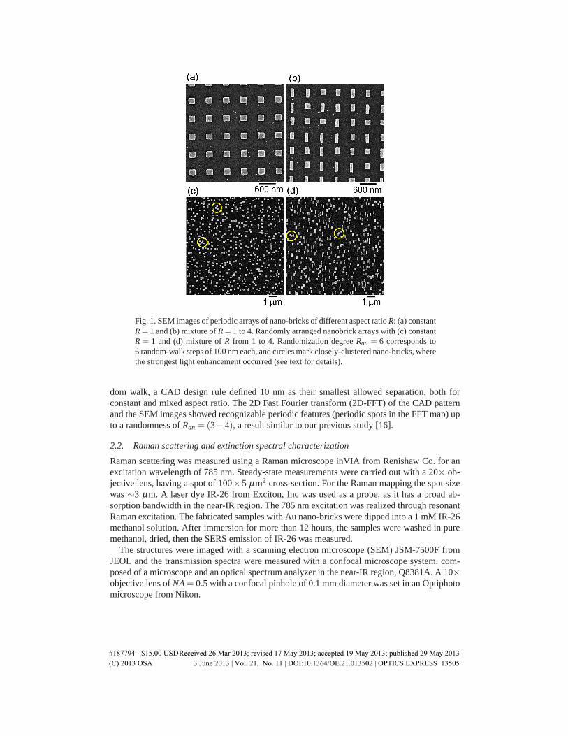
Fig. 1. SEM images of periodic arrays of nano-bricks of different aspect ratio R: (a) constantR = 1 and (b) mixture of R = 1 to 4. Randomly arranged nanobrick arrays with (c) constantR = 1 and (d) mixture of R from 1 to 4. Randomization degree Ran = 6 corresponds to6 random-walk steps of 100 nm each, and circles mark closely-clustered nano-bricks, wherethe strongest light enhancement occurred (see text for details).
dom walk, a CAD design rule defined 10 nm as their smallest allowed separation, both forconstant and mixed aspect ratio. The 2D Fast Fourier transform (2D-FFT) of the CAD patternand the SEM images showed recognizable periodic features (periodic spots in the FFT map) upto a randomness of Ran = (3−4), a result similar to our previous study [16].
2.2. Raman scattering and extinction spectral characterization
Raman scattering was measured using a Raman microscope inVIA from Renishaw Co. for anexcitation wavelength of 785 nm. Steady-state measurements were carried out with a 20× ob-jective lens, having a spot of 100×5 μm2 cross-section. For the Raman mapping the spot sizewas ∼3 μm. A laser dye IR-26 from Exciton, Inc was used as a probe, as it has a broad ab-sorption bandwidth in the near-IR region. The 785 nm excitation was realized through resonantRaman excitation. The fabricated samples with Au nano-bricks were dipped into a 1 mM IR-26methanol solution. After immersion for more than 12 hours, the samples were washed in puremethanol, dried, then the SERS emission of IR-26 was measured.
The structures were imaged with a scanning electron microscope (SEM) JSM-7500F fromJEOL and the transmission spectra were measured with a confocal microscope system, com-posed of a microscope and an optical spectrum analyzer in the near-IR region, Q8381A. A 10×objective lens of NA = 0.5 with a confocal pinhole of 0.1 mm diameter was set in an Optiphotomicroscope from Nikon.
#187794 - $15.00 USDReceived 26 Mar 2013; revised 17 May 2013; accepted 19 May 2013; published 29 May 2013(C) 2013 OSA 3 June 2013 | Vol. 21, No. 11 | DOI:10.1364/OE.21.013502 | OPTICS EXPRESS 13505

Fig. 2. Extinction spectra of the periodic array of nano-bricks with aspect ratio from 1to 4, with the indicated light polarization. The L- and T-modes are shown together with thenon-polarized light measurement (black line). Extinction scale is the same for all patterns.
2.3. Finite difference time domain simulations
Numerical modeling of light enhancement on a large area of nano-bricks was carried out withthe 3D-FDTD method implemented with the Lumerical software from FDTD Solutions. Thesubstrates were modeled as glass layers on which the gold nano-bricks were placed accordingto the layout and dimensions specified in the CAD pattern file, which was imported for thecalculations. The refractive index spectra of the materials were fitted from the experimentalvalues obtained in literature, by means of a built-in polynomial model.
To obtain reasonable use of computational resources without sacrificing accuracy, a sectionof the substrate of 11×11 periods was modeled, included in a FDTD domain closed in all direc-tions by perfectly matched layers (PMLs) to avoid spurious reflections. A central area of 5×5periods was illuminated by a total-field scattered-field (TFSF) source, to measure separately thetotal field in the central area, and the field scattered outside. This also increases PML efficiency,as it only has to absorb the weaker scattered field instead of the total one. The simulated layoutsare: (i) regular array Ran = 0 of 600 nm period of regular square nano-bricks of 200×200 nm(R = 1), (ii) random array Ran = 6 of regular nano-bricks, (iii) regular array of mixed aspectratio nano-bricks (R from 1 to 4), and (iv) random array of mixed nano-bricks. In the cases (ii)and (iv), since the nano-bricks cannot cross the TFSF source boundary lest simulation accuracyis compromised, their position is slightly adjusted; this does not influence the modeling resultssignificantly due to the large total number of nano-bricks inside the simulation domain.
The simulations were performed on the swinSTAR supercomputer at Swinburne University,having nodes of 16 cores and 64 GB memory each. The memory footprint was around 200 GBand took about 6 hours to run on a 16-node cluster for a total of 256 cores.
#187794 - $15.00 USDReceived 26 Mar 2013; revised 17 May 2013; accepted 19 May 2013; published 29 May 2013(C) 2013 OSA 3 June 2013 | Vol. 21, No. 11 | DOI:10.1364/OE.21.013502 | OPTICS EXPRESS 13506

Fig. 3. Experimental SERS spectra of IR-26 adsorbed on gold nano-bricks of periodic pat-tern but different aspect ratio R. Note the difference in the vertical scale between the panels.
3. Results
3.1. Extinction and SERS of periodic and random patterns
We fabricated 65-nm-tall Au nano-bricks in order to recover a better shape closer to the de-signed rectangular cross-section. Figure 1 shows SEM images of Au nano-bricks with differentaspect ratios and of their random mixtures. The volume of the Au nano-bricks was kept con-stant for each aspect ratio, with a 600 nm period for the periodic arrays. In the random patterns,some nano-bricks are adjoined, since the 10 nm separation enforced in the CAD pattern couldnot be exactly reproduced in the fabricated patterns.
Figure 2 shows the experimental extinction spectra of the nano-bricks of constant aspectratio variable from 1 to 4. With increasing aspect ratio, the longitudinal L-mode resonancewavelength red-shifts while the transversal T-mode blue-shifts. Since the volume of the Aunano-bricks is kept constant, a narrowing of the width causes an expected blue-shift of theT-mode, and likewise the longer rods show a red-shift of the L-mode. The geometry of nano-bricks and patterns were chosen to have extinction maxima in the near-IR spectral region, wherethe dye SERS measurements were carried out.
First, periodic patterns of constant aspect ratio nano-bricks were investigated. Figure 3 showsthe Raman scattering spectra of the IR-26 laser dye adsorbed on the Au nano-bricks. StrongRaman peaks specific to IR-26 appeared from 800 to 1600 cm−1. The absolute value of theRaman intensities varies for each pattern and follows the extinction values. The SERS signalshows electromagnetic and chemical enhancements: the electromagnetic effect closely followsthe extinction spectrum. Therefore, by normalizing the SERS signal to extinction at the exci-tation and Raman scattering wavelengths, it is possible to unveil other field enhancement orquenching contribution, if present. This is important, since the intricacies of SERS enhance-ment are still strongly debated in literature [27, 28].
The normalized SERS intensity at 1558 cm−1 is shown in Fig. 4 for patterns of differentaspect ratio. The experimentally measured SERS intensity is divided by the extinction value atthe irradiation and Raman scattering wavelengths. Then, it is normalized to the SERS intensity
#187794 - $15.00 USDReceived 26 Mar 2013; revised 17 May 2013; accepted 19 May 2013; published 29 May 2013(C) 2013 OSA 3 June 2013 | Vol. 21, No. 11 | DOI:10.1364/OE.21.013502 | OPTICS EXPRESS 13507

Fig. 4. Normalized SERS signal as a function of aspect ratio R for the periodic patterns.The SERS signal was normalized to the extinction values at the excitation and Stokes1558 cm−1 wavelengths; then, the value was further normalized to the SERS signal ob-tained on a periodic square (aspect ratio R = 1) pattern.
value of the periodic square nano-brick structures (R = 1). Such normalization is expectedto bring out the effect of SERS contributions from hot-spots, since the spectrally narrow andstrongly spatially localized light field enhancement is averaged in the extinction measurements.The intensity of the T-mode has a tendency to increase with the aspect ratio, however the L-mode is almost constant or somewhat decreased as compared with the periodic R = 1 pattern.This behavior is understandable from the analysis of the extinction spectra shown in Fig. 2.The local field factor is proportional to the extinction at the wavelengths of excitation andscattering. The local E-field at the hot-spots (edges or/and gaps) shows an electromagneticenhancement factor L(ν) = |Eloc(ν)|/|E0|, where E0 is the incident light E-field amplitude.The SERS scattered power is given as [29]:
Ps(νs) = NσSERSL(νl)2L(νs)
2I(νl), (1)
where the field enhancements at the excitation and Raman scattering wavelengths (frequencyνl,s = c/λl,s) are considered; here N is the number of scatterers, σSERS is the SERS scatte-ring cross-section, I is the irradiation intensity. Since usually the laser and Raman wavelengthsare similar, the total enhancement factor is assumed to be R ≡ L(νl)
2L(νs)2 � |Eloc|4/|E0|4.
However, as shown in Fig. 2, this rule cannot be used when there are considerable extinctionvariations. This is also a very important factor for measurement of local temperature in nano-gaps, from the ratio of Stokes to anti-Stokes Raman peaks, where the SERS signal has to benormalized to extinction at the excitation and Raman scattering wavelengths [30].
Next, SERS on random arrays of nano-bricks was investigated. A random mixture of struc-tures with aspect ratios varying from 1 to 4 was fabricated for SERS. Typical extinction spectraare shown in Fig. 5. Periodic (randomness Ran = 0) nano-square structures show spectral broad-ening of the extinction peaks with increasing randomness. Due to nanoparticle symmetry, theextinction has no polarization dependence. In the case of nano-bricks, which originally havea polarization dependence of extinction when their aspect ratio R > 1, the polarization depen-dence persists with pattern randomization and shows broadening (Fig. 5).
The cumulative effect of randomness Ran and aspect ratio R of nano-brick patterns for SERSintensity is summarized in Fig. 6, where the resonant Raman spectra are presented, normal-ized by extinction at excitation (785 nm) and Raman scattering (894 nm corresponding to1558 cm−1) wavelengths. The Raman intensity of the 1558 cm−1 peak shows dependence onboth Ran and R. Interestingly, SERS intensity increased with increasing randomness for both
#187794 - $15.00 USDReceived 26 Mar 2013; revised 17 May 2013; accepted 19 May 2013; published 29 May 2013(C) 2013 OSA 3 June 2013 | Vol. 21, No. 11 | DOI:10.1364/OE.21.013502 | OPTICS EXPRESS 13508

Fig. 5. Polarization dependence of the extinction spectra for the periodic (top-row) andrandom Ran = 6 (bottom-row) arrangements of (a) square nano-bricks, and (b) nano-brickswith aspect ratio varying from R = 1 to 4.
Fig. 6. SERS intensity maps of the major 1558 cm−1 Raman mode. On the vertical axis isthe randomness Ran = 0 (periodic) to 6 and on the horizontal one is the maximum aspectratio of the pattern, from R = 1 (squares) to 4 (seven different patterns changing in steps of0.5, see Fig. 5. The plots show the polarization dependence of (a) L-mode and (b) T-mode.
the L- and T-mode. The experimentally observed enhancement reached 4× for the T-mode.Randomization with Ran = 6 gave a 2× enhancement as compared with periodic patterns ofR = 1 and Ran = 0. This is in good agreement with numerical simulations presented in Sec. 3.2.
This additional enhancement is due to hot-spot formation as a result of pattern randomization,as we recently showed [16]. SERS mapping was carried out on patterns of different aspect ratioand randomization coefficient. The spot diameter and stepping distance were ∼3 μm. Resultsfor periodic and random patterns are shown in Fig. 7. All samples were measured for T-modeexcitation, to have a better comparison between different patterns at the excitation wavelength.
In the case of periodic structures with nano-bricks of the same aspect ratio, the SERS mapswere flat over the fabricated 100×100 μm2 region (Fig. 7). The average SERS count rate wasapproximately 2000 with a min-to-max span of ±100. When different aspect ratio nano-brickswere mixed, weak hot-spot-like spikes began to emerge. This is due to the broken periodicitydue to nano-bricks of different widths, however this did not affect the overall average, but rather
#187794 - $15.00 USDReceived 26 Mar 2013; revised 17 May 2013; accepted 19 May 2013; published 29 May 2013(C) 2013 OSA 3 June 2013 | Vol. 21, No. 11 | DOI:10.1364/OE.21.013502 | OPTICS EXPRESS 13509

Fig. 7. SERS mapping at the 1558 cm−1 Raman wavelength for (a) periodic pattern withR = 1, (b) periodic pattern with mixture of R = 1 to 4, (c) random pattern with R = 1,and (d) random pattern with mixture of R = 1 to 4. The random pattern has randomnessRan = 6. Note that for all panels the SERS intensity scale is the same from 0 to 8000; thefootprint of the SERS region was 100×100 μm2.
the min-to-max span, which increased to ±500.The pattern randomization had a stronger effect on the average SERS intensity and the spikes
which follow the surface distribution of the hot-spots. This is the experimental evidence of hot-spot formation due to randomization. The strongest SERS was observed on the patterns whichare fully randomized and have the widest range of nano-bricks of different aspect ratios. It isobvious that stronger enhancement occurred between bricks separated by few nanometers. Theexcitation spot areas (φ ∼ 3 μm) interrogates 20 ∼ 30 nanoparticles and the Raman intensityis averaged, however, we can clearly recognize the high intensity spot by mapping. The Ramanmapping method is useful for searching the regions where hot-spots are formed. The averageSERS count rate was approximately ∼2500 with maxima ∼1000 counts higher. Next, the ex-perimentally observed trends are numerically corroborated by 3D finite-element time-domain(3D-FDTD) simulations.
3.2. Numerical simulations of field enhancement
The numerical results are shown in Fig. 8, where the calculated extinction cross-sections showsimilar behaviors as the experimental ones in Fig. 5. Simulated nano-bricks have exact shape;when the experimental extinction of 0.4 is normalized to a numerical cross-section of 10 cal-culated on a 25-brick cluster and normalized the the total gold area in the cluster, differencescan be safely attributed to fabrication tolerances. In particular, the slight difference between L-and T-mode for layout (ii) all but disappears in the experiment, while in layout (iii) and (iv)the randomization broadening is less pronounced in the simulation. In the latter case, the T-and L-mode peaks are slightly blue-shifted in the experiment, suggesting that the fabricatednano-bricks are actually smaller, possibly due to fabricated corners being rounded.
The SERS intensity has been estimated from the calculated field enhancement and cross-
#187794 - $15.00 USDReceived 26 Mar 2013; revised 17 May 2013; accepted 19 May 2013; published 29 May 2013(C) 2013 OSA 3 June 2013 | Vol. 21, No. 11 | DOI:10.1364/OE.21.013502 | OPTICS EXPRESS 13510

Fig. 8. Extinction cross-sections numerically calculated for the periodic (top-row) and ran-dom Ran = 6 (bottom-row) arrangements of a 25-element cluster of (a) square nano-bricks,and (b) nano-bricks with aspect ratio varying from R = 1 to 4. The cross-sections are nor-malized to the total geometrical area of the gold in the cluster (black dashed line).
sections at the excitation and Raman wavelengths for the L- and T-mode, according to thelayouts (i) to (iv), which correspond to the four corners of the panels in Fig. 6. For the T-modethe trend is clearly confirmed as, where the normalized value is 1 for layout (i), for layout (ii)it is 9× (2× experimental), for (ii) it is 6× (2.5× exper.), and for (iv) it is 10× (4.5× exper.).The simulated results for the T-mode are 2∼3 times higher than the experimental ones, this isinfluenced by the numerically perfect definition of corners and interfaces, giving results thatcan be considered upper performance bounds for a finely tuned fabrication process.
Figure 9 shows the field enhancement distributions for the best-case T-mode (layout (iv) andL-mode (layout (ii)), as compared with layout (i) at the Raman scattering wavelength of 894 nm.The top panels show the field cut in the xy-plane flush with the top of the nano-bricks, whilethe bottom panels show the field cut in the vertical plane crossing the centre of the array andparallel to the excitation polarization. The square box shows the total-field region encompassingthe 25 nano-blocks on which the cross-sections are calculated, while outside of it the scatteredfield is visible. The plots for layout (i) in Fig. 9 (a,d) show a wide distribution of the long-rangecoupled optical energy, insensitive to the x or y polarization direction, for a maximum fieldenhancement of 7×10³ on the top of the nano-bricks, when extinction cross-section values aretaken into account. This climbs to 7.1×10⁴ for the T-mode on layout (iv) in Fig. 9 (b,e), wherethe scattering appears short-ranged and asymmetrical; the vertical-plane cut shows how the fewhot-spots corresponding to nano-bricks very close to each other scatter very strongly both in airand in the substrate. This is true to an extent also for the L-mode on layout (ii) in Fig. 9 (c,f),where the adjusted enhancement reaches 4.2×10³.
4. Discussion
The spectra shown in Fig. 2 can be modeled theoretically by harmonic oscillators whose dis-sipation rate as a function of dispersion can be written as αL,T ∼ γ(ω)/[(ω −ωL,T )
2 − γ2(ω)],where the resonant frequencies ωL,T are determined mostly by geometry, and the scatteringrate γ is strongly frequency-dependent. The longitudinal resonance always has lower resonantfrequency decreasing with increase in aspect ratio R, as the longitudinal electric field gets pro-gressively less contained inside the metal nano-bricks, and the restoring force driving the os-cillation decreases. Similarly, the transverse resonance is always blue-shifted relative to the
#187794 - $15.00 USDReceived 26 Mar 2013; revised 17 May 2013; accepted 19 May 2013; published 29 May 2013(C) 2013 OSA 3 June 2013 | Vol. 21, No. 11 | DOI:10.1364/OE.21.013502 | OPTICS EXPRESS 13511

Fig. 9. E-field intensity enhancement log-scale maps numerically calculated for (a,d) pe-riodic layout (i) as compared with the highest enhancement condition for (b,e) T-mode(random layout (iv) and (c,f) L-mode (random layout (ii). The field sections are (top) xy-plane flush with the top of the nano-bricks and (bottom) vertical plane crossing the arraycenter and parallel to the excitation polarization. The white dashed lines show (top) the po-sition of the vertical plane sections and (bottom) the glass-air boundary. The box shows thetotal-field region, while outside the scattered field can be seen. Contour lines show constantintensity enhancement (1 for dark green, 10 for dark yellow).
longitudinal one, because the transverse field tends to get progressively more contained insidethe metal, thus increasing the restoring force. The resonant frequencies can be reasonably wellfitted using a rough analytical model for the ellipsoid from [31] to estimate the depolarizationfactors NL,T , and then use the data for the real part of the dielectric constant of gold εr(ω)from [32] to obtain the resonant frequencies from the equation:
NL,T [εr(ωL,T )−1] = 1. (2)
The fact that the imaginary part of the gold dielectric constant εi(ω), and hence the damp-ing rate, increases rapidly at wavelengths shorter than 700 nm, as well as the increase of ra-diative loss proportional to ω2, leads to a strong asymmetry of the extinction spectra, with apronounced shelf in the short wavelength region, as well as a general suppression of the trans-verse peak relative to the longitudinal one. The spectra also appear not fully Lorentzian andthat comes from the dipole-dipole coupling between the particles. Following the theory of [21],we estimate the broadening imposed by dipole coupling to be about ΔωL,T ∼ ωL,T (d/a)3 ∼0.03ωL,T , where d is the distance between the nano-bricks and a is their characteristic dimen-sion. This broadening due to coupling (or one can say plasmon tunneling between the particles)thus amounts to about 30 nm, compared to the broadening due to damping γ(ω) that is muchlarger, on the order of 100-150 nm; hence, one can consider most surface plasmons to be local-ized on either one or maybe two particles, even in the absence of disorder which would causeeven farther localization. But also, as our previous work [34] has shown, there can be a fewdelocalized modes in which the resonant energy transfer can lead to the formation of hot-spotsin which the field gets concentrated.
Figure 4 shows an interesting result as the ratio of Raman intensity to the square of intensityenhancement grows with the increase of aspect ratio R for the transverse polarization, whilesuch a striking difference in the normalized spectra can be explained by the fact that total
#187794 - $15.00 USDReceived 26 Mar 2013; revised 17 May 2013; accepted 19 May 2013; published 29 May 2013(C) 2013 OSA 3 June 2013 | Vol. 21, No. 11 | DOI:10.1364/OE.21.013502 | OPTICS EXPRESS 13512

extinction is proportional to the integral of∫
Metal |Eloc|2/|E0|2dV over the fraction of SPP modeinside the metal, where the electrons that actually dissipate the energy (both radiatively andnon-radiatively) are located, while Raman intensity is proportional to
∫Dye |Eloc|4/|E0|4dV (the
integral is over the volume of SPP mode where the dye molecules are located). The ratio plottedin Fig. 4 is then proportional to
∫Dye |Eloc|4dV/
(∫Metal |Eloc|2dV
)2and tends to increase for
more uneven distribution of electric field, which is the feature of transverse modes at larger R,as the energy tends to concentrate near the corners.
Consider that, if I(x,y,z) is the local E-field intensity, the normalization of Fig. 4 correspondsto evaluating the ratio 〈I(x,y,z)2〉/〈I(x,y,z)〉2, which in essence measures the non-uniformityof the intensity distribution by building an estimator of its variance as a stochastic process andnormalizing it by its average [33].
In Fig. 5(a) one can see the extinction spectrum variation caused by the randomness. Accord-ing to [21], the strong randomness value of 6 (Fig. 1(c)) cannot be treated as a small perturbation– but its impact can nevertheless be quickly estimated by observing that it is the relatively largenumber of pairs of nano-bricks that nearly touch each other, that experience the largest shiftof their resonance frequencies, on the order of ΔωL,T ∼ ωL,T (a/2a)3 ∼ ωL,T/8, which makesthis coupling-induced broadening comparable to the original damping-induced broadening. Asa result, the spectra at the bottom differ dramatically from those at the top. When it comes tothe impact of randomness on the extinction spectrum of the mixed nano-bricks in Fig. 5(b), theimpact of disorder in placement is about the same as disorder in shape, that already broadensthe upper Fig. Hence, the difference between the lower and upper Figs. is not as large as inFig. 5(a).
Raman enhancement is shown in Fig. 6. It is clear that the normalized Raman efficiencyincreases with randomness for both L- and T-modes, but in a different fashion. For both modes,one can identify the enhancement with the hot-spots that occur wherever the nicely coupleddimer or trimer is formed. Then, as shown in ref. [34], first the dipole mode of a larger nanobrickget excited with field enhancement of as much as Q-factor of the mode (Q � 5 in this work).Following that the energy get resonantly transferred to smaller nanobricks and then to narrowgaps between them. Each time excitation is transferred to the dipole mode of a smaller particleor to the gap mode the field gets additional enhancement by a factor of Q. Since the Ramanenhancement is proportional to the fourth power of the field, one can easily see that it can beas high as Q12 ∼ 2× 10⁸ or higher. All in all, it is rather difficult to predict in advance whichcluster will offer larger enhancement, hence by randomization we greatly increase the chance ofgetting just the right combinations for the hot-spots, as shown in the circles Fig. 1. Now, whenit comes to elongated nano-bricks, statistically there is higher probability for them to align ina way to form a smaller gap for the T-mode than for the L-mode – therefore, for the T-modethe largest Raman enhancement takes place for larger R, while for the L-mode it is the R = 1square nano-bricks that have the strongest Raman enhancement.
As one can see from the experimental data in Fig. 7 and the numerical results of Fig. 9,the hot spots are not distributed uniformly over the surface, and the highest density of them isindeed found when one has non-uniform distribution of both shapes and positions of the nano-bricks, resulting in the highest probability of having a local arrangement of bricks that is mostfavorable for field enhancement, such as dimers and trimers with narrow gaps between them.These results indicate that designing optimum SERS substrates is a far from trivial process, andperhaps randomization and disorder offer a good route to achieve a good performance, whichmay not be the best theoretically possible result, but is the one that can be reliably achieved.
#187794 - $15.00 USDReceived 26 Mar 2013; revised 17 May 2013; accepted 19 May 2013; published 29 May 2013(C) 2013 OSA 3 June 2013 | Vol. 21, No. 11 | DOI:10.1364/OE.21.013502 | OPTICS EXPRESS 13513

5. Conclusions
In this study, we experimentally observed resonance SERS enhancement induced by random-ization of nano-brick patterns. The SERS intensity increased approximately twice when nano-bricks of different aspect ratios were intermixed. An additional 4 times enhancement was ob-served by randomization of periodic patterns. Formation of strongly localized hot-spots wasconfirmed by SERS mapping and by 3D-FDTD simulations. The observed SERS enhance-ment is consistent with spectral and spatial localization of light field induced by randomiza-tion [21, 34]. Fabrication of random nano-patterns and nano-textured surfaces usually requiresless elaborated fabrication techniques, e.g., dry plasma etching for nano-textured Si [35], andfavors practical applications in harvesting of solar energy and in bio-/medical sensing.
Acknowledgments
YN gratefully thanks Prof. Toshihiko Baba from Yokohama National University for fruitfuldiscussions and granting access to fabrication and characterization facilities. This work wasfinancially supported by the Research Foundation for Opt-Science and Technology. SJ is grate-ful for support via Australian Research Council DP130101205 project. Part of this work wasperformed on the swinSTAR supercomputer at Swinburne University of Technology.
#187794 - $15.00 USDReceived 26 Mar 2013; revised 17 May 2013; accepted 19 May 2013; published 29 May 2013(C) 2013 OSA 3 June 2013 | Vol. 21, No. 11 | DOI:10.1364/OE.21.013502 | OPTICS EXPRESS 13514