raspberry pi for data acquisition michael allan (f) · pdf fileraspberry pi for data...
TRANSCRIPT
Raspberry Pi for Data Acquisition
by
Michael Allan (F)
Fourth-year undergraduate project
in Group A, 2012/2013
I hereby declare that, except where specifically indicated, the work
submitted herein is my own original work.
Signed: Date:

Raspberry Pi for Data Acquisition Michael Allan, Fitzwilliam College
Technical Abstract
This project aimed to develop a data acquisition (DAQ) system based on the Raspberry Pi.
Existing DAQ systems depend on the procurement and maintenance of a computer, which
can be very expensive, therefore a replacement for the computer is desirable. While a device
such as a mobile phone has enough processing power to perform DAQ tasks, the Raspberry
Pi presents an attractive prospect due to the combination of low cost and many options for
connectivity.
Several off the shelf DAQ solutions were examined to see how they could potentially
perform when connected to a Raspberry Pi. While it was seen that significant cost savings
could still be made, the performance of these systems was not very strong. A system based
on custom hardware would more fully exploit the potential of the Raspberry Pi. A
specification for this system was conceived that would be feasible but would out-perform
current commercial offerings.
The form this hardware would take was then designed – some form of analogue interface to
take samples, and then a buffer to compensate for the Raspberry Pi’s lack of a Real-Time
operating system. For communication between the custom hardware (the PiDAQ) and the
Raspberry Pi, the SPI bus was selected from the available options. As the buffer, an ARM
Cortex-M3 based microprocessor from STmicroelectronics was selected, since it had
sufficient power for the application and would allow the buffer and analogue sampling
stages to be integrated.
The rest of the circuit was then designed around this chip; firstly the ancillary support
circuitry, secondly the interface between the differential analogue inputs and the analogue
to digital converters (ADCs) of the microprocessor, thirdly an additional digital interface,
fourthly the various power supplies, and finally the connectors and physical interfaces.
The software that would be required was then designed, falling into two parts: embedded
software that would run on the microprocessor, and application software that would run on
the Raspberry Pi. The embedded software was designed to make use of interrupts and DMA
(Direct Memory Access) to minimise the load on the microprocessor and reduce the
complexity of the program code. The application software designed such that the storage
engine (responsible for interfacing with the custom hardware) and the controller (the user
Raspberry Pi for Data Acquisition Michael Allan, Fitzwilliam College
interface) would communicate over the network and be capable of being run on separate
machines. The embedded software would be programmed in C using the CMSIS libraries, the
application software would be written in Python using Twisted for networking, matplotlib
for graph creation, and protobufs for data storage and interchange.
With the design complete the hardware was sent to be manufactured, and prototyping began
on the software using a Phidget interface. Once the hardware was completed development
continued in stages as more features were added to the software. Much of the development
time was spent attempting to improve the performance of the sample acquisition process
and data displays on the Raspberry Pi, where the simple design choices made proved
inadequate. During this process some errors in the hardware manufacture were discovered,
but these did not impact significantly on the project.
In the end it was not possible to achieve the full specification of 20 kHz sampling on four
channels. It was possible to transfer 20 kSamples/s into the Raspberry Pi, which limits the
system to 5 KHz per channel, or 20 kHz on one channel. There is scope to improve
performance further, but there was not time to do so during the project.
The difficulties encountered in achieving the target sample rate meant some of the more
advanced targets of the project were not met: no revision was made to the hardware to add
dedicated interfaces for thermocouples and the like, as originally planned, and the user
interface is more rudimentary and has less features than was desired. Implementing these
targets provides ample scope for future work.
In conclusion, the project was a success in demonstrating that data acquisition could be
performed with the Raspberry Pi with reasonable performance, but to exceed the
performance of current commercial systems more development time would be needed.
Contents
1 Introduction 3
1.1 The Raspberry Pi ............................................................................................................... 4
1.2 Potential Systems ............................................................................................................. 5
1.3 Specification ....................................................................................................................... 5
1.4 Project Plan ......................................................................................................................... 6
1.4.1 PiDAQ Mk I
1.4.2 PiDAQ Mk II
1.4.3 System Software
1.4.4 User Software
2 System Design 8
2.1 Hardware ............................................................................................................................. 8
2.1.1 Communication
2.1.2 Serial Peripheral Interface
2.1.3 Data Acquisition
2.1.4 Microprocessor Support Circuitry
2.1.5 Programming Interface
2.1.6 ADC Interface
2.1.7 Digital Input/output
2.1.8 Power Supplies
2.1.9 Physical Interfaces and PCB Design
2.2 Software ............................................................................................................................ 19
2.2.1 Programming Environment
2.2.2 Overall Structure
2.2.3 Embedded Software
2.2.4 Direct Memory Access (DMA)
2.2.5 Hardware Abstraction
2.2.6 Storage Engine
2.2.7 Communication Protocol
2.2.8 User Interface/Controller
2 Raspberry Pi for Data Acquisition
3 System Implementation Process 28
3.1 Phidgets ............................................................................................................................ 28
3.2 PCB Assembly .................................................................................................................. 28
3.3 Firmware Bootstrap ...................................................................................................... 29
3.4 Version Control ............................................................................................................... 30
3.5 Raspberry Pi Operating System ................................................................................ 30
3.6 Peripheral Configuration ............................................................................................. 31
3.7 Increasing the Sample Rate ....................................................................................... 32
3.8 16-bit Transfers ............................................................................................................... 34
3.9 Analogue Sampling ....................................................................................................... 34
3.10 User Interface .................................................................................................................. 35
3.11 Digital I/O ......................................................................................................................... 36
3.12 Final User Interface ....................................................................................................... 36
4 Testing 37
5 Conclusions 39
5.1 Future Work ...................................................................................................................... 40
6 Bibliography 41
Appendix A Circuit Schematic 42
Appendix B PCB Design 47
Appendix C Risk Assessment Retrospective 50
Introduction 3
1 Introduction The aim of the project was to build a laboratory data acquisition system, suitable for both
teaching and research use, based on the Raspberry Pi.
The motivation for this stemmed from the high cost of implementing a commercially
available data acquisition system from scratch. The key (and most prohibitive) cost inherent
in such a system is a computer to run the experiment. Most users of such systems are
already equipped with a suitable machine, but this is probably used day-to-day for many
other purposes and it is impractical to tie it up with running data acquisition for any length
of time. Since the cost of an additional machine, both in capital and in support, is high,
organisations are reluctant to fund them and even if they do it takes valuable resources away
from areas where they are more required. The computing power required for performing
data acquisition and rudimentary processing is not high, and a dedicated DAQ PC is likely to
be using a fraction of its available power on the task.
A second motivating factor is underutilisation of the interface part of the DAQ system,
converting sensor signals and sending them to the computer to be recorded, or in some
cases using instructions from the computer to control the experiment. Even the simplest
interfaces cost more than $100 and require proprietary software for which an additional
licence is required. In many experiments, particularly those used for teaching, this cost is
seen as prohibitive and leads to the sharing of DAQ equipment between groups, or even
avoiding its use entirely, thus reducing teaching labs to the tedium of watching a stop-clock
while writing down the occasional reading.
Given these two issues, we can attack the lack of a suitable DAQ system from both ends.
There are some less well known examples of DAQ interfaces that are cheaper and are
compatible with non-proprietary systems for recording, storing, and processing the data, but
these still require a PC.
The initial idea behind this project was to replace the computer with a device such as a
smartphone. This would drastically reduce the size and complexity of the PC side of the DAQ
system. However, when the Raspberry Pi was announced this was seen as an even better
candidate.
4 Raspberry Pi for Data Acquisition
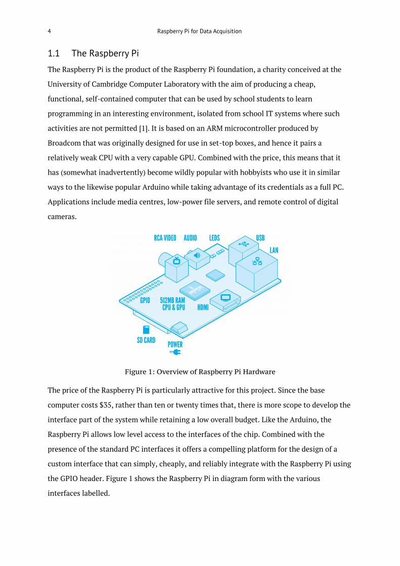
1.1 The Raspberry Pi
The Raspberry Pi is the product of the Raspberry Pi foundation, a charity conceived at the
University of Cambridge Computer Laboratory with the aim of producing a cheap,
functional, self-contained computer that can be used by school students to learn
programming in an interesting environment, isolated from school IT systems where such
activities are not permitted [1]. It is based on an ARM microcontroller produced by
Broadcom that was originally designed for use in set-top boxes, and hence it pairs a
relatively weak CPU with a very capable GPU. Combined with the price, this means that it
has (somewhat inadvertently) become wildly popular with hobbyists who use it in similar
ways to the likewise popular Arduino while taking advantage of its credentials as a full PC.
Applications include media centres, low-power file servers, and remote control of digital
cameras.
Figure 1: Overview of Raspberry Pi Hardware
The price of the Raspberry Pi is particularly attractive for this project. Since the base
computer costs $35, rather than ten or twenty times that, there is more scope to develop the
interface part of the system while retaining a low overall budget. Like the Arduino, the
Raspberry Pi allows low level access to the interfaces of the chip. Combined with the
presence of the standard PC interfaces it offers a compelling platform for the design of a
custom interface that can simply, cheaply, and reliably integrate with the Raspberry Pi using
the GPIO header. Figure 1 shows the Raspberry Pi in diagram form with the various
interfaces labelled.
Introduction 5
1.2 Potential Systems
Having established that the Raspberry Pi could support either the connection of a traditional
DAQ interface, such as those made by National Instruments (NI), or a custom piece of
hardware, a number of potential solutions were analysed to see what could be possible. From
internet searching, some potential candidates were found and examined.
NI produces a USB DAQ, the NI USB-6008 [2]. This supports 8 analogue inputs at 12 bit
resolution and 10 kS/s (samples per second) and costs $99. To utilise its full functionality,
however, requires NI LabVIEW which is not feasible for use with the Raspberry Pi. Another
company, Phidgets Inc., produce devices that support a single specific kind of sensor on a
USB port, or that have several analogue inputs like a traditional DAQ interface [3]. They
have the advantage of being programmable with a Python API, which is a supported
programming language for the Raspberry Pi. At $80, the interfaces are slightly cheaper than
NI’s, but the sampling rate of 1 kS/s is not considered to be fast enough. A further company,
DATAQ, produces similar types of devices to the Phidgets and with similar performance to
the NI interface, but for an accordingly higher price [4].
Given the capabilities of the Raspberry Pi and the types of systems currently available on the
market, it was felt that producing a custom interface was an appropriate option, both from
the point of view of creating a system to fit the brief and from the point of view of making
the project itself interesting and challenging. This custom system has been christened the
PiDAQ.
1.3 Specification
The following specification was chosen for the PiDAQ system:
Hardware (Analogue Interface)
0-10V Input Voltage Range
20 kS/s Sampling Frequency
12 Bit Resolution
4 Input Channels
Software (Internal and User Facing)
‘Open’ formats for data storage and
interchange
Compatible with MATLAB and LabVIEW
Use TCP/IP network communications to
give a distributed system.
6 Raspberry Pi for Data Acquisition
This specification was chosen to meet the needs of experiments in thermodynamics and to
be comparable with the existing systems described above. It was initially desired that the
final form of the project would exceed these specifications, for example by directly
supporting sensors such as thermocouples or Wheatstone bridges without the need for an
external amplifier.
The software specification was more open-ended. At a minimum the data from the
Raspberry Pi should be collected and then could be passed to a separate package for
processing, which could vary in complexity from an Excel spreadsheet to MATLAB. It was
desired, however, that the software would be able to intuitively control the system and
present live data, and that the full functionality of the Raspberry Pi could be exploited.
1.4 Project Plan
The project was divided into four milestones, two for hardware and two for software. It was
expected that the hardware and software milestones would be worked on concurrently.
1.4.1 PiDAQ Mk I
This was a basic PCB, supporting analogue input and connecting to the Raspberry Pi’s GPIO
header. This milestone was intended to demonstrate the interface to the Raspberry Pi and
provide a building block for the PiDAQ Mk II. It was targeted to be completed by the start of
Lent term.
1.4.2 PiDAQ Mk II
This was intended to be a more advanced PCB, an evolution of the Mk I to fix any issues and
to add the capability to interface with specialist sensors directly, which would be a key
advantage of the PiDAQ over the competing products. This milestone was targeted for the
end of Lent term, but due to problems encountered with the software development the Mk II
was never designed.
1.4.3 System Software
This was the software that runs on the PiDAQ to send readings to the Raspberry Pi, and the
software that runs on the Raspberry Pi to receive, store and distribute this data. This
milestone was targeted for three weeks after the completion of PiDAQ Mk I, partway
through Lent term.
Introduction 7
1.4.4 User Software
This formed the user interfaces to configure, start, and stop the PiDAQ, and the interfaces
for display of the recorded data. There was also the possibility of expanding to include the
capability to perform pre-processing of data before export to a full analysis workflow (for
example, it may be considered useful to be able to filter the data or to view spectrograms of
it in real time during or shortly after capture). This milestone was targeted for the end of the
Easter holiday. Due to the slow development of the system software the functionality of the
User Software was reduced.
8 Raspberry Pi for Data Acquisition
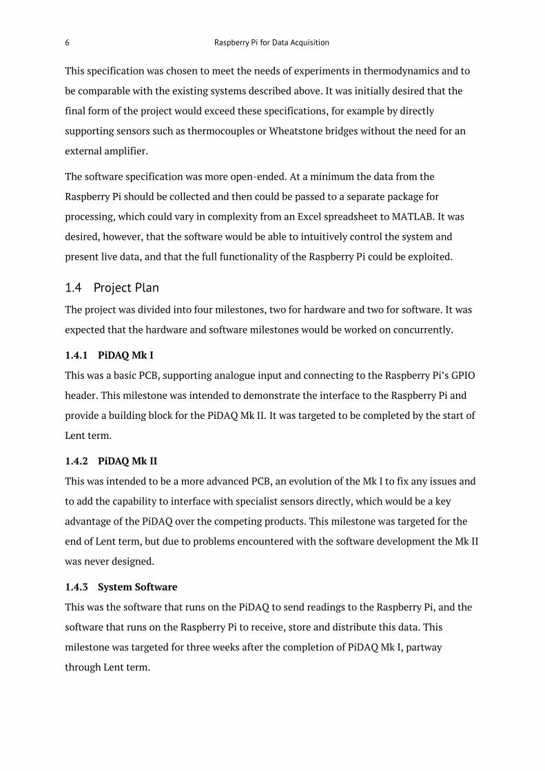
2 System Design This section describes the designs developed for the PiDAQ Mk I hardware and the
associated software (both embedded and on the Raspberry Pi).
2.1 Hardware
The hardware had two goals – to obtain the data by sampling the inputs and to
communicate this data to the Raspberry Pi host.
Figure 2: Block Diagram of PiDAQ System
Table 1: Bill of Materials for PiDAQ
Part Description Quan-tity
C1-6, C8-11, C13, C16, C22
Capacitor, Multi-Layer Ceramic, 0603, X7R, 50V, 100nF 13
C7 Capacitor, Multi-Layer Ceramic, 0805, X5R, 6V3, 10uF 1 C12, C17, C18, C19, C20
Capacitor, Multi-Layer Ceramic, 0603, X5R, 25V, 1uF 5
C14, C15 Capacitor, Multi-Layer Ceramic, 0603, NP0, 50V, 15pF 2 C21 Capacitor, Multi-Layer Ceramic, 0603, X7R, 25V, 330nF 1 D1, D2, D3 LED, SMD, 0805, Red 3 P1 Header, Straight, 10 Way, Dual Row, JTAG 1 P2 Terminal Block, 8 Way Wago Cage Clamp 1 P3 Header, 10-Pin, Samtek Cortex Debug 1 P4, P5 Header, 3-Pin, 0.1” Pitch 2

System Design 9
Part Description Quan-tity
P6 Header, 26-Pin, Dual row, 0.1” Pitch 1 P7 Header, 4-Pin, Dual row, 0.1” Pitch 1 R1, R3, R5, R7, R15-17 Resistor, Thick Film, 10K 1% 0603 0.063W 7 R2, R4, R6, R8 Resistor, Thick Film, 47K 1% 0603 0.063W 4 R9-13 Resistor, Thick Film, 10K 1% 0603 0.063W 5 R14 Resistor, Thick Film, 470R 1% 0603 0.063W 1 R18, R19, R20 Resistor, Thick Film, 100R 1% 0603 0.063W 3 S1 Switch, Pushbutton, Surface Mount 1 U1, U2, U3, U4 AD8275 G = 0.2, Level Translation, 16-Bit ADC Driver 4 U5 TXB0108 8-Bit Bidirectional Voltage-Level Translator
with Auto Direction Sensing 1
U6 STM32F103RBT6 ARM-based 32-bit MCU Performance Line with 128 kB Flash, 20 kB Internal RAM, -40 to +85°C Temperature, 64-Pin LQFP
1
U7, U8 Low Quiescent Current LDO, 3.3V, 3-Pin SOT-23 2 U9 5V to 9V Single Output DC/DC Converter 1 U10 Positive Voltage Regulator, 5V, 4-Pin SOT-89 1 Y1 Crystal, 8MHz 18pF 1
The full schematic and PCB layout for the hardware are included as Appendix A and
Appendix B. This section contains the rationale for component selection and the design
decisions made.
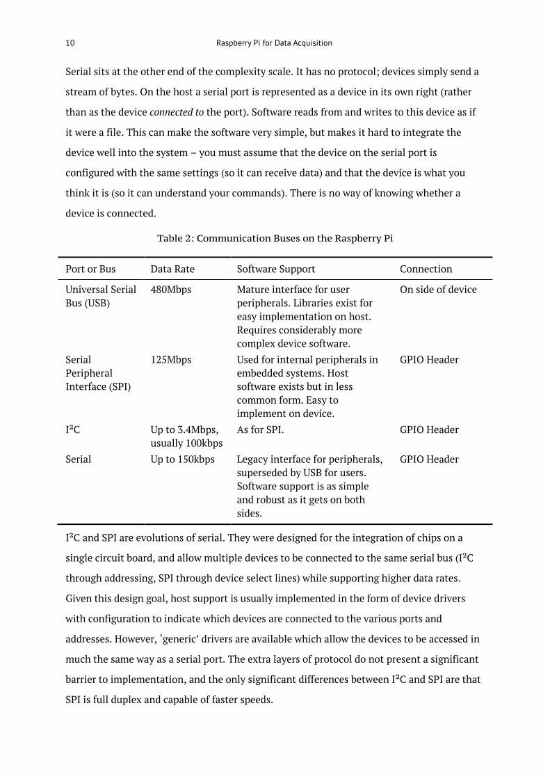
2.1.1 Communication
For communication, the PiDAQ could be connected by any of the several ports on the
Raspberry Pi. Table 2 shows these for comparison. Each has both benefits and drawbacks.
USB is an interface commonly used to connect peripherals to devices, and is used by every
alternative off the shelf solution considered above in section 1.2. It is very fully featured,
allowing auto detection of devices by the host and several different communications
channels between the host and device. The complexity that is its major benefit is also its
biggest drawback – implementing the software to support this protocol is complex and time
consuming, and the advanced features are poorly documented. Another factor to consider is
the number of USB ports on the Raspberry Pi: there are only two available which are
commonly used for mouse and keyboard. Utilising one of these for the PiDAQ would require
the purchase and use of a USB hub for input.
10 Raspberry Pi for Data Acquisition
Serial sits at the other end of the complexity scale. It has no protocol; devices simply send a
stream of bytes. On the host a serial port is represented as a device in its own right (rather
than as the device connected to the port). Software reads from and writes to this device as if
it were a file. This can make the software very simple, but makes it hard to integrate the
device well into the system – you must assume that the device on the serial port is
configured with the same settings (so it can receive data) and that the device is what you
think it is (so it can understand your commands). There is no way of knowing whether a
device is connected.
Table 2: Communication Buses on the Raspberry Pi
Port or Bus Data Rate Software Support Connection
Universal Serial Bus (USB)
480Mbps Mature interface for user peripherals. Libraries exist for easy implementation on host. Requires considerably more complex device software.
On side of device
Serial Peripheral Interface (SPI)
125Mbps Used for internal peripherals in embedded systems. Host software exists but in less common form. Easy to implement on device.
GPIO Header
I²C Up to 3.4Mbps, usually 100kbps
As for SPI. GPIO Header
Serial Up to 150kbps Legacy interface for peripherals, superseded by USB for users. Software support is as simple and robust as it gets on both sides.
GPIO Header
I²C and SPI are evolutions of serial. They were designed for the integration of chips on a
single circuit board, and allow multiple devices to be connected to the same serial bus (I²C
through addressing, SPI through device select lines) while supporting higher data rates.
Given this design goal, host support is usually implemented in the form of device drivers
with configuration to indicate which devices are connected to the various ports and
addresses. However, ‘generic’ drivers are available which allow the devices to be accessed in
much the same way as a serial port. The extra layers of protocol do not present a significant
barrier to implementation, and the only significant differences between I²C and SPI are that
SPI is full duplex and capable of faster speeds.
System Design 11
Given these characteristics, SPI was the most suitable bus to use. USB is too complex, and
serial is too simple and slow. The SPI bus had the additional advantage of being located on
the GPIO header, which would allow easier mechanical integration of the system.
2.1.2 Serial Peripheral Interface
The SPI bus is based on a master/slave architecture and uses three main signals: a clock and
two data lines. The master device generates the clock (SCK line). The data lines are MOSI
(Master Out Slave In) and MISO (Master In Slave Out); together they give full duplex
communications. To allow several slave devices to be connected to a single bus, SPI devices
usually feature chip select lines, one per slave device, which must be controlled to enable
only the slave the master wishes to communicate with. This control circuit is often built into
the SPI master peripheral, and on the Raspberry Pi the SPI bus has two built-in select lines.
An SPI device is usually implemented with a pair of shift registers, one for each data line,
both clocked from SCK.
Transfers are always full duplex, so it is not possible to transmit without receiving, or to
receive without transmitting. A full duplex transfer always occurs, but not all the data
transferred has to be meaningful. The higher level protocol running over SPI must be aware
of this.
2.1.3 Data Acquisition
There were several possible alternatives for the data acquisition part of the system, and the
characteristics of the Raspberry Pi were important again here. The host is not running a real
time operating system (RTOS), so care must be taken to ensure that sampling is consistent
and continuous even when the host is performing other tasks. For example, many SPI-based
analogue to digital converters (ADCs) have their timing set by the SPI clock, with no internal
timing. While the device is being read from they return data, stopping if the bus is inactive.
This means that an uninterrupted stream of reads must be issued, something difficult
without an RTOS even if a dedicated device driver was written.
To resolve this, a buffer between the sampling and the communication was required,
ensuring that sampling could continue when the Raspberry Pi was performing other tasks.
At this point microprocessors enter into contention.

12 Raspberry Pi for Data Acquisition
Almost every microprocessor incorporates the SPI bus. Some are more powerful than others,
in speed or functionality, but the field of potential candidates is huge and reducing it is
difficult.
The sampling rate being targeted in this application was not very high, and the bit depth was
also limited. It was therefore reasonable to limit the search to those microprocessors with
built-in ADCs, eliminating the need for a dedicated chip. In this situation the
microprocessor acts as both the buffer and the data sampler.
Neither power consumption nor cost were significant considerations. The application
processor on Raspberry Pi itself would almost certainly dominate the power consumption of
the overall system, and we are not concerned with battery-powered applications. The price
point that the PiDAQ system would be competing with is not very restrictive either. The
microprocessor would be the only expensive chip in the system, so a large portion of the
budget could be dedicated to it.
There are only a few dominant microprocessor families, more so for these embedded
processors than for desktop PC processors, but limited nonetheless. Microchip produces an
extensive family of PIC processors, which have simpler architectures. Atmel have a slightly
more complex architecture, and target similar markets to Microchip (Atmel processors
power the popular Arduino platform). ARM-based processors form a third major player –
ARM core designs are used by several major manufacturers such as NXP, STMicroelectronics
and Texas Instruments, each integrating the core with a different set of peripherals. ARM-
based microprocessors are capable 32-bit cores but use more power and have historically
been higher cost.
For this project the decision was made to base the system around an ARM processor
manufactured by STMicroelectronics. This was based on several factors in addition to the
raw processing power, such as the availability of free, high quality development tools and
standard peripheral libraries. The cost was reasonable, even in low quantities and
particularly when considering large-scale manufacturability. ST processors also integrate
high quality ADC peripherals when compared with competitor’s implementations of the
same core. The processing speed meant that the microprocessor should not end up
representing the bottleneck of the overall system.

System Design 13
The particular processor chosen was the STM32F103. The F1 series integrates ARM’s Cortex-
M3 core, designed for embedded applications where power is not critical. Figure 3 shows the
various features of processors in this series. The F103 line is the ‘Performance’ line, with the
best selection of integrated peripherals including the desired ADC capabilities. The initial
system was designed around the RBT6 variant, which is a 64-pin QFP package with 20
Kbytes of SRAM and 128 Kbytes of flash memory. This was almost certainly larger, in terms
of pin count and memory, than would be required for the system to operate, but it is easier
to subsequently reduce the size of the chip than it is to make it larger after producing a
prototype, especially when there is no easy way to estimate the memory requirements of the
software.
Since the processor had the spare capability, one of its UART serial ports was also connected
through to the Raspberry Pi for debugging purposes. This gave the possibility of
reprogramming the microprocessor from the Raspberry Pi.
Figure 3: The STM32 F1 Family
2.1.4 Microprocessor Support Circuitry
Any microprocessor requires some ancillary circuitry, and the more complex the
microprocessor the more circuitry it requires. To prevent the high speed internal switching
from coupling onto the power supplies, decoupling capacitors are required on every power
pin. The manufacturer recommends a 100nF ceramic capacitor on each power pin for this
14 Raspberry Pi for Data Acquisition
purpose [5, p. 7]. To prevent rail droop when peripherals are switched on and off, one of the
power pins must also have a larger 10µF tantalum or electrolytic capacitor. The ADC
peripheral has separate power pins, which are decoupled with 100nF and 1µF capacitors. All
decoupling capacitors must be physically placed as close as possible to the pins in question
to have maximum benefit.
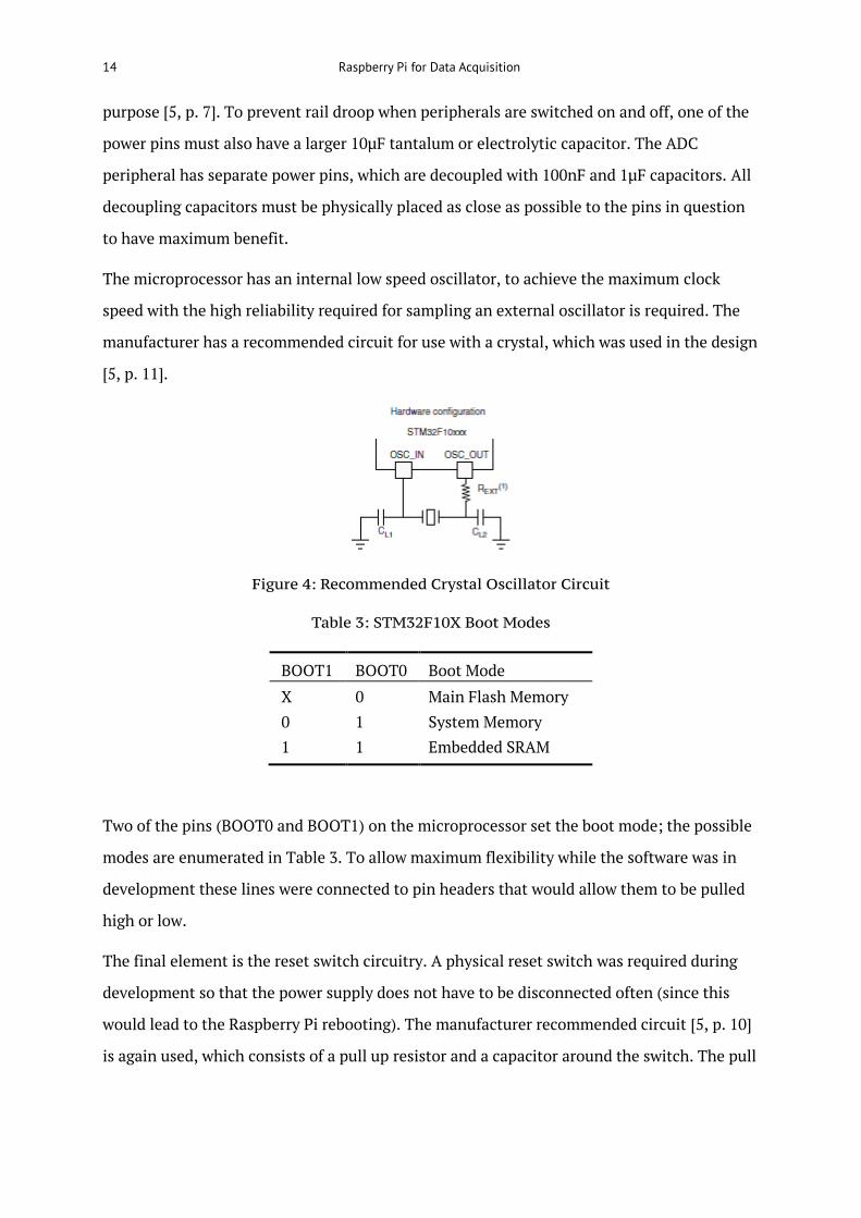
The microprocessor has an internal low speed oscillator, to achieve the maximum clock
speed with the high reliability required for sampling an external oscillator is required. The
manufacturer has a recommended circuit for use with a crystal, which was used in the design
[5, p. 11].
Figure 4: Recommended Crystal Oscillator Circuit
Table 3: STM32F10X Boot Modes
BOOT1 BOOT0 Boot Mode X 0 Main Flash Memory 0 1 System Memory 1 1 Embedded SRAM
Two of the pins (BOOT0 and BOOT1) on the microprocessor set the boot mode; the possible
modes are enumerated in Table 3. To allow maximum flexibility while the software was in
development these lines were connected to pin headers that would allow them to be pulled
high or low.
The final element is the reset switch circuitry. A physical reset switch was required during
development so that the power supply does not have to be disconnected often (since this
would lead to the Raspberry Pi rebooting). The manufacturer recommended circuit [5, p. 10]
is again used, which consists of a pull up resistor and a capacitor around the switch. The pull
System Design 15
up is not strictly required as the device has an internal pull up resistor. The capacitor
protects against parasitic resets caused by EMI.
2.1.5 Programming Interface
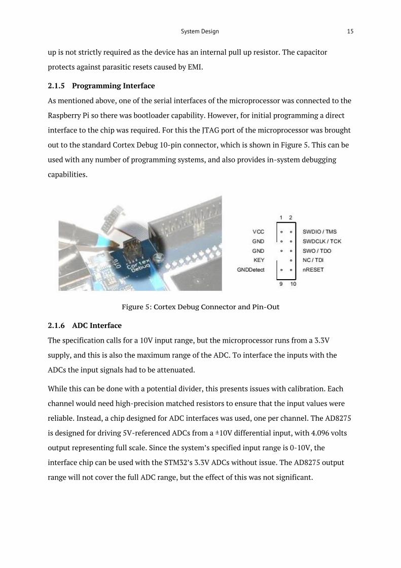
As mentioned above, one of the serial interfaces of the microprocessor was connected to the
Raspberry Pi so there was bootloader capability. However, for initial programming a direct
interface to the chip was required. For this the JTAG port of the microprocessor was brought
out to the standard Cortex Debug 10-pin connector, which is shown in Figure 5. This can be
used with any number of programming systems, and also provides in-system debugging
capabilities.
Figure 5: Cortex Debug Connector and Pin-Out
2.1.6 ADC Interface
The specification calls for a 10V input range, but the microprocessor runs from a 3.3V
supply, and this is also the maximum range of the ADC. To interface the inputs with the
ADCs the input signals had to be attenuated.
While this can be done with a potential divider, this presents issues with calibration. Each
channel would need high-precision matched resistors to ensure that the input values were
reliable. Instead, a chip designed for ADC interfaces was used, one per channel. The AD8275
is designed for driving 5V-referenced ADCs from a ±10V differential input, with 4.096 volts
output representing full scale. Since the system’s specified input range is 0-10V, the
interface chip can be used with the STM32’s 3.3V ADCs without issue. The AD8275 output
range will not cover the full ADC range, but the effect of this was not significant.
16 Raspberry Pi for Data Acquisition
While the specification of the system is only for single ended inputs, the attenuators support
differential inputs. To make use of this functionality the system had a differential input on
each channel, with a jumper to tie one side to ground for single ended operation.
So that the board had the capability to run with the full input range of the AD8275s,
provision was made on their outputs for a potential divider. If this is used care will have to
be taken with resistor choice so as not to impact on accuracy.
2.1.7 Digital Input/output
The processor has a high pin count. Even with four ADCs and the four pins of the SPI
interface taken, a large number were unused. To use these leftovers, a digital interface was
also added, providing eight digital inputs or outputs. This uses a bidirectional level shifter
chip so that the outputs are driven or read using the more standard 5V logic level. The bi-
directionality means that input or output can be selected on a pin-by-pin basis. There are
many such chips that have suitable performance, the TXB0108 from Texas Instruments was
chosen on the basis of price and availability.
Two more outputs are provided in the form of LEDs – these were useful for debugging and
testing to provide visual indication of status.
2.1.8 Power Supplies
The system required power at two voltages – 3.3V for the microprocessor and level shifter,
and 5V for the AD8275 attenuators and the level shifter output. It was desirable to take
power from the Raspberry Pi rather than requiring a second external power supply.
The Raspberry Pi is powered from a 5V USB phone charger-style adapter. This means that
the 5V supply coming onto the board is noisy and of variable quality. The simplest way to
deal with this is by linear regulation, but you cannot regulate 5V to 5V linearly. Therefore, a
DC to DC converter module was included in the design to convert initially from the 5V USB
supply to a 9V rail. This is then down-regulated by three regulators, one 5V to power the
AD8275s and the TXB0108, and two 3.3V, one for the ADC supply for the microprocessor
and another to power the chip itself and the output of the level shifter.
The system was also designed with separate analogue and digital grounds, joined at a single
point. These measures ensured that each power supply on the board was isolated from the
Raspberry Pi and was as high quality as possible.

System Design 17
2.1.9 Physical Interfaces and PCB Design
The components above were assembled onto a custom PCB. This allows surface-mount
components to be used (where stripboard or veroboard do not) and is considerably easier to
design for a system which requires good noise immunity and large numbers of
interconnects. The design was four-layer (two outer signal layers and two inner power
planes). While the complexity of the system was such that it may have been possible to
design it as two-layer, the internal power planes gave a large advantage for noise immunity
and made the design process much easier and quicker. It is also not significantly more
expensive to manufacture.
There were three user-facing physical interfaces of the system (the JTAG port formed a
fourth used only in development). The board must first connect to the Raspberry Pi’s GPIO
port for the serial, SPI and power connections. This connector was a 0.1 inch pitch, 26 pin, 2
row header. There also had to be connectors for the analogue inputs and digital I/O.
While it would have been possible to use a ribbon cable to connect to the GPIO port, the
design had a sufficiently small footprint to mount directly to the Raspberry Pi with a socket
header on the bottom of the board. This made for a robust, compact system, but it did place
limitations on the PCB shape as the board must fit around the Raspberry Pi’s connectors –
the GPIO header is lower than the USB, Ethernet, and composite video ports. It would have
been possible to extend out over the audio header, but this would have created a
mechanically fragile spur on the board. This shape was inspired by the Pi-Face digital
input/output board. [6]
Figure 6: The Pi-Face Digital I/O Board
18 Raspberry Pi for Data Acquisition
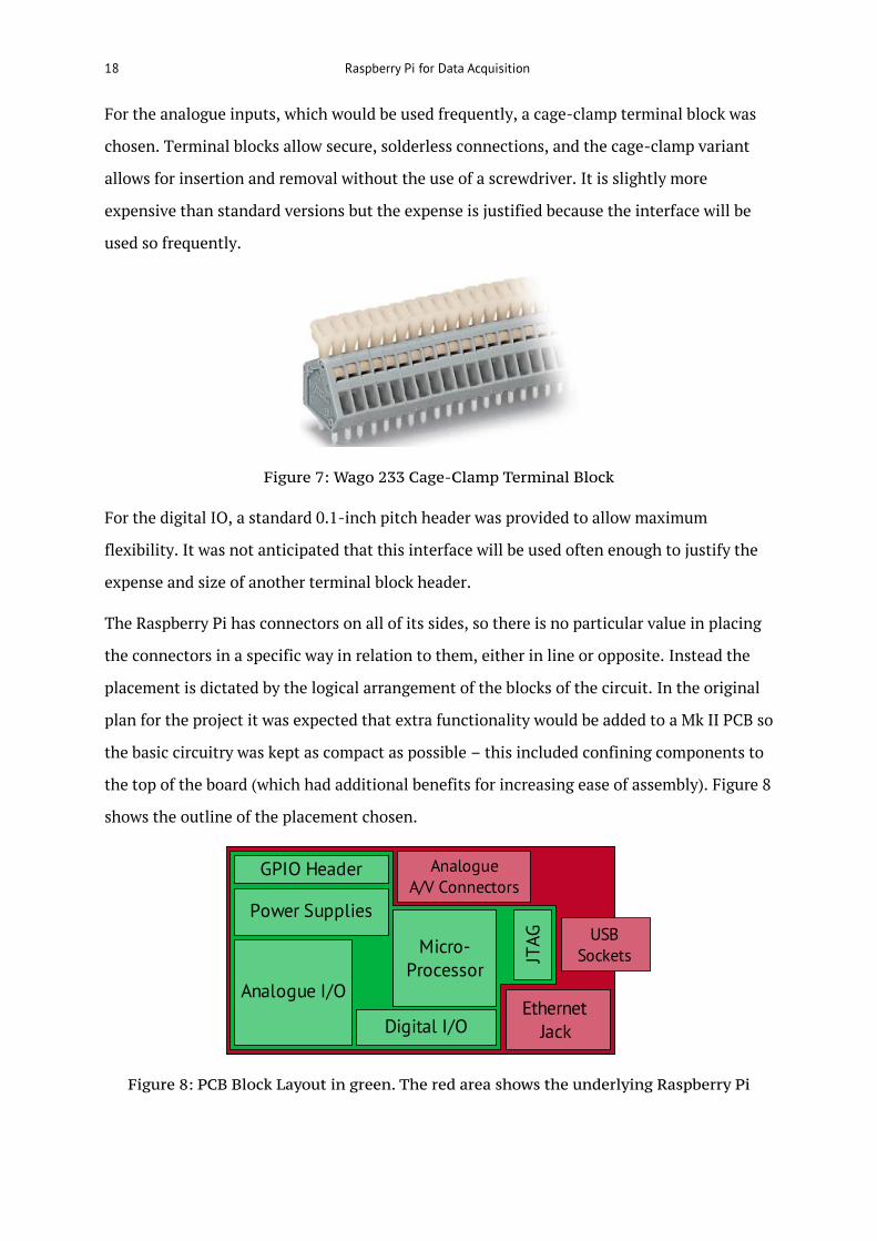
For the analogue inputs, which would be used frequently, a cage-clamp terminal block was
chosen. Terminal blocks allow secure, solderless connections, and the cage-clamp variant
allows for insertion and removal without the use of a screwdriver. It is slightly more
expensive than standard versions but the expense is justified because the interface will be
used so frequently.
Figure 7: Wago 233 Cage-Clamp Terminal Block
For the digital IO, a standard 0.1-inch pitch header was provided to allow maximum
flexibility. It was not anticipated that this interface will be used often enough to justify the
expense and size of another terminal block header.
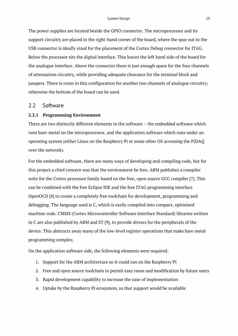
The Raspberry Pi has connectors on all of its sides, so there is no particular value in placing
the connectors in a specific way in relation to them, either in line or opposite. Instead the
placement is dictated by the logical arrangement of the blocks of the circuit. In the original
plan for the project it was expected that extra functionality would be added to a Mk II PCB so
the basic circuitry was kept as compact as possible – this included confining components to
the top of the board (which had additional benefits for increasing ease of assembly). Figure 8
shows the outline of the placement chosen.
Figure 8: PCB Block Layout in green. The red area shows the underlying Raspberry Pi
GPIO Header
Power Supplies
JTAGMicro-
Processor
Digital I/O
Analogue I/O
AnalogueA/V Connectors
USBSockets
EthernetJack
System Design 19
The power supplies are located beside the GPIO connector. The microprocessor and its
support circuitry are placed in the right-hand corner of the board, where the spur out to the
USB connector is ideally sized for the placement of the Cortex Debug connector for JTAG.
Below the processor sits the digital interface. This leaves the left hand side of the board for
the analogue interface. Above the connector there is just enough space for the four channels
of attenuation circuitry, while providing adequate clearance for the terminal block and
jumpers. There is room in this configuration for another two channels of analogue circuitry;
otherwise the bottom of the board can be used.
2.2 Software
2.2.1 Programming Environment
There are two distinctly different elements to the software – the embedded software which
runs bare-metal on the microprocessor, and the application software which runs under an
operating system (either Linux on the Raspberry Pi or some other OS accessing the PiDAQ
over the network).
For the embedded software, there are many ways of developing and compiling code, but for
this project a chief concern was that the environment be free. ARM publishes a compiler
suite for the Cortex processor family based on the free, open source GCC compiler [7]. This
can be combined with the free Eclipse IDE and the free JTAG programming interface
OpenOCD [8] to create a completely free toolchain for development, programming and
debugging. The language used is C, which is easily compiled into compact, optimised
machine code. CMSIS (Cortex Microcontroller Software Interface Standard) libraries written
in C are also published by ARM and ST [9], to provide drivers for the peripherals of the
device. This abstracts away many of the low-level register operations that make bare metal
programming complex.
On the application software side, the following elements were required:
1. Support for the ARM architecture so it could run on the Raspberry Pi
2. Free and open source toolchain to permit easy reuse and modification by future users
3. Rapid development capability to increase the ease of implementation
4. Uptake by the Raspberry Pi ecosystem, so that support would be available

20 Raspberry Pi for Data Acquisition
Due to advances in popularity of the ARM architecture, (1) and (2) are no longer significant
limitations. ARM publishes compilers for Linux platforms in the same way as they do for the
bare metal embedded platform. (3) limits selection to higher level languages, for example
C++, Java or Python. (4) leads to a choice of Python – as an interpreted language its
capabilities for rapid development are second to none, and it is in use on the Raspberry Pi
platform as a key teaching language. Community support is available and there are pre-
written libraries for driving the Raspberry Pi’s GPIO port.
As a bonus, the Eclipse IDE also has Python development and debugging capabilities so a
single IDE could be used to work on both parts of the software simultaneously.
For data interchange, the protobuf format was selected [10]. This is a data interchange
format designed by Google, initially for internal use and later made open source. It allows
for space-efficient encoding of data, with backward and forward compatibility built in as the
data format changes.
A protobuf message contains any number of fields, which can be numeric, textual or even
nested protobuf messages. The messages are defined in a proprietary language, which is
then compiled to generate Python code that can be used to create, decode and edit instances
of the messages. If the message definition changes to add new fields, older programs using
that message can ignore the new data without causing errors.
To manage the networking aspects of the program, the Twisted network API was selected
[11]. This allows simple implementation of clients and servers with shared code to describe
the protocol that exists between them. It also has timers and multithreaded programming
capabilities which will be used in other parts of the program. The API is also cross platform,
allowing identical code to run on Windows or Linux.
To create user interfaces, the wxWidgets toolkit was selected [12]. This is cross platform and
lightweight, has a mature Python API, and is easily integrated with the Twisted networking
API. The latter is necessary as both frameworks are event driven, so need to have compatible
polling loops.
System Design 21
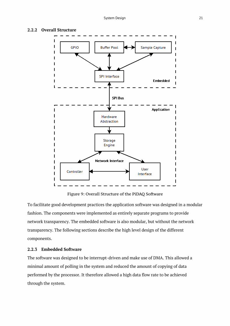
2.2.2 Overall Structure
Figure 9: Overall Structure of the PiDAQ Software
To facilitate good development practices the application software was designed in a modular
fashion. The components were implemented as entirely separate programs to provide
network transparency. The embedded software is also modular, but without the network
transparency. The following sections describe the high level design of the different
components.
2.2.3 Embedded Software
The software was designed to be interrupt-driven and make use of DMA. This allowed a
minimal amount of polling in the system and reduced the amount of copying of data
performed by the processor. It therefore allowed a high data flow rate to be achieved
through the system.

22 Raspberry Pi for Data Acquisition
Figure 10: Data Flow through Embedded Software
The ADC peripheral on the STM32 can operate in single, continuous or scan modes. Its 16
input channels are multiplexed together into a single converter. In single mode, a single
channel is converted once and the result stored in registers. In continuous mode, a single
channel is converted continuously with the end of one conversion triggering another
conversion. In scan mode a group of channels is converted in sequence a single time, with
DMA used to transfer the results to memory.
Data enters the program in the sampling module, where the ADC conversion is triggered by
a timer module. This ensures that the sampling is as regular as possible. The ADC is
programmed to convert all four channels at once, using DMA to place the results in a
temporary buffer. The ADC captures continuously into this buffer. When it is half full of new
samples, a DMA interrupt is triggered and they are emptied out into a buffer from the buffer
pool to pass through the rest of the system.
When a buffer of samples is ready it is added to the full buffer queue to be sent over SPI. SPI
transmission can only occur when the bus master (the Raspberry Pi) is requesting data, so
there must be a queue here in case there is a gap between requests. The system samples
System Design 23
continuously when powered on, but can only send data to the Raspberry Pi when it is
requested.
The program’s main loop keeps the SPI module loaded with a buffer for transmission,
waiting for a request to come in from a Raspberry Pi. It does this by polling to see if the
previous transfer has completed. The SPI module uses DMA to copy the current buffer into
the SPI peripheral for transmission as transfers are initiated by the Raspberry Pi.
The SPI peripheral is operating in slave mode, so all timing is derived from the clock signal
emitted by the Raspberry Pi. The module is configured for 16 bit words and has a one-word
transmit and receive buffer. During a transmit/receive cycle these are shifted out and in
from the MISO and MOSI SPI lines respectively (see section 2.1.2 above). Since this is such a
small buffer the DMA is critical in ensuring that data is always available to be sent and that
no received data is lost.
With SPI it is not possible to receive without transmitting, so after a buffer has been sent
and before the next buffer is ready the module sends a continuous stream of null bytes.
Without this the last byte to be sent is repeated in response to any further requests.
The buffer pool manages the cycle of memory – a buffer is the fundamental division of data
used throughout the program. It maintains a list of potential buffers, returning a free one in
response to a request and recycling buffers whose data has been processed. Accesses of the
buffer pool must be managed with care to ensure that if the pool routines are interrupted by
another routine the program does not enter an inconsistent state.
2.2.4 Direct Memory Access (DMA)
The sampling process on the microprocessor makes extensive use of the STM32’s DMA
controller. The alternative would be to interrupt on each sample or SPI word transferred.
The DMA controller and processor core share the same memory bus, which means that while
a DMA operation is occurring the processor cannot be running. A carefully programmed
interrupt approach could therefore be as fast and reliable as the DMA.
Despite the lack of performance improvement, DMA is still used where possible as it allows
simpler code to be written, with fewer timing critical interrupt routines.
24 Raspberry Pi for Data Acquisition
2.2.5 Hardware Abstraction
The storage engine forms the interface between the custom microprocessor hardware and
the user interface. It must poll the microprocessor for samples and store them either
temporarily or permanently. Since the main logic of the storage engine is written in Python,
a Python extension is required to interface to the Linux SPI drivers, which are usually
accessed from C.
One of the reasons for selecting SPI as a protocol was that it is possible to avoid writing a
device driver. The kernel has a built in generic driver called spidev. This has an interface
based around the ioctl system call, and a simple Python extension written in C can proxy SPI
operations from Python to this interface [13].
2.2.6 Storage Engine
To enable easy management of large numbers of samples, a stream of samples is divided into
blocks. Each block stores a number of samples for a single channel along with some
metadata. A block is sized so that, if written to disk, it gives a file of reasonably small size. It
is desired to store data in several small files rather than one large one for several reasons:
1. It aids data recovery in the event of file corruption, since not all files will be lost.
2. File systems have limits on maximum file size, so very large data sets it would have to
be split anyway.
3. It makes it possible to process data before the logging session has finished by
accessing the files that have already been written.
4. If the storage engine experiences an error, most data will already have been written
to disk so data loss is minimised.
5. When searching through data, only one file’s worth needs be read and processed at a
time.
The block pool maintains a number of blocks in the memory of the process to avoid
repeated memory allocations, recycling them as appropriate. The flow of a block through the
pool is as follows:
1. The polling logic has no room for more samples in its current block, so requests a
new one.
2. The block pool finds the oldest reusable block and sends it to the polling loop to fill.

System Design 25
3. When the block is full it is returned to the pool.
What happens next depends on whether a logging session is in progress. If it is desired to
save the recorded data, the block is marked with persist. When a block that is marked in this
way it is returned to the pool and added to the queue to be written out to disk, setting the
written flag once this has been done. The block is written as a protobuf for efficient binary
encoding. This is less accessible than using a format such as CSV, but the space efficiency
saving is worth the extra effort in translating protobufs for use in other programs.
When determining which block to reuse for new data, the least recently used block is sent. If
the data is not being recorded, this creates a rolling buffer equal in size to the block pool for
use in live previewing, or to capture data from before the user starts a session (i.e. if waiting
for a given event, run with the rolling buffer until it occurs then trigger the recording, saving
samples which have already been taken). If data is being recorded, a block is only reused
once it has been written. If no block is free then the program has experienced a buffer
overflow and will terminate to ensure that the user is aware of possible data corruption.
The storage engine also maintains an index of which blocks contain which time periods of
sample data. This index includes blocks that form part of a capture sequence, but have been
written to disk and are no longer stored in memory. All blocks are allocated a UUID
(Universally Unique Identification Number) which is used both in the index and also to name
the block files when written to disk. A query interface to the storage engine allows an
arbitrary time period of samples to be retrieved, reading them back from disk if they are no
longer in memory.
2.2.7 Communication Protocol
The communication protocol is simple and is concentrated around getting data over the SPI
bus with minimal overhead. The ADC output is twelve bits long, but the SPI word size is 16
bits. The four spare bits are used as a header with non-sample information.
Table 4 shows the structure of data packets returned from the microprocessor to the
Raspberry Pi. The high bit of the first word is set to indicate ‘start of frame’ this allows the
two devices to synchronise if they are not initialised simultaneously (for example if the
Raspberry Pi software is restarted, there may still be sample data in the microprocessor
transmit buffer that must be expunged). The first byte sent is the header that indicates how
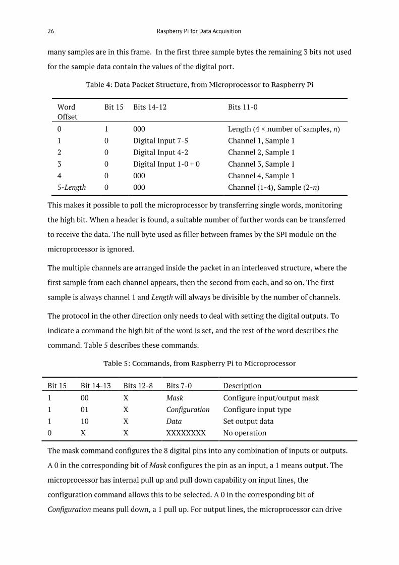
26 Raspberry Pi for Data Acquisition
many samples are in this frame. In the first three sample bytes the remaining 3 bits not used
for the sample data contain the values of the digital port.
Table 4: Data Packet Structure, from Microprocessor to Raspberry Pi
Word Offset
Bit 15 Bits 14-12 Bits 11-0
0 1 000 Length (4 × number of samples, n) 1 0 Digital Input 7-5 Channel 1, Sample 1 2 0 Digital Input 4-2 Channel 2, Sample 1 3 0 Digital Input 1-0 + 0 Channel 3, Sample 1 4 0 000 Channel 4, Sample 1 5-Length 0 000 Channel (1-4), Sample (2-n)
This makes it possible to poll the microprocessor by transferring single words, monitoring
the high bit. When a header is found, a suitable number of further words can be transferred
to receive the data. The null byte used as filler between frames by the SPI module on the
microprocessor is ignored.
The multiple channels are arranged inside the packet in an interleaved structure, where the
first sample from each channel appears, then the second from each, and so on. The first
sample is always channel 1 and Length will always be divisible by the number of channels.
The protocol in the other direction only needs to deal with setting the digital outputs. To
indicate a command the high bit of the word is set, and the rest of the word describes the
command. Table 5 describes these commands.
Table 5: Commands, from Raspberry Pi to Microprocessor
Bit 15 Bit 14-13 Bits 12-8 Bits 7-0 Description 1 00 X Mask Configure input/output mask 1 01 X Configuration Configure input type 1 10 X Data Set output data 0 X X XXXXXXXX No operation
The mask command configures the 8 digital pins into any combination of inputs or outputs.
A 0 in the corresponding bit of Mask configures the pin as an input, a 1 means output. The
microprocessor has internal pull up and pull down capability on input lines, the
configuration command allows this to be selected. A 0 in the corresponding bit of
Configuration means pull down, a 1 pull up. For output lines, the microprocessor can drive
System Design 27
them in both push-pull and open-drain modes. A 1 means open-drain and 0 puts the
corresponding pin into push-pull mode.
On initialisation, all pins are configured as pulled-down inputs (Mask = Configuration = 0).
The data command sets the value of any of the pins configured as outputs. Bits
corresponding to input pins are ignored.
2.2.8 User Interface/Controller
The user interface needed to have the following basic functionality:
1. Start and stop logging sessions
2. View live data before and during logging sessions
3. View past sessions and their data
4. Export the data to other formats for further processing
To accomplish the control functions, a protocol based on a protobuf message was designed–
the control message has several Boolean fields to indicate the type of command being
executed, and other optional fields to describe the command arguments such as a session id
or a time range. The storage engine can then respond with a similar message containing
either further information or data samples, or both.
To implement live view, the controller polls the storage engine for recent samples at a
regular interval, which are then displayed on a graph in a rolling buffer (in the same sense as
samples are stored in a rolling buffer by the storage engine).
To view data, the matplotlib library for Python was selected [14]. This library has an
extensive repertoire of functions for drawing all types of graphs, and has the ability to
selectively modify the displayed data (known as ‘animation’ in the documentation) which is
useful for displaying rapidly changing live sample data.

28 Raspberry Pi for Data Acquisition
3 System Implementation Process
3.1 Phidgets
The PiDAQ PCB having been designed, it was desirable to begin writing the application
software while the PCB was manufactured by a commercial service (a process which takes
two weeks). To accomplish this, a Phidget interface was procured, such as the one described
in section 1.2. While it was not capable of the same data rates, the type of data received was
the same. Within the modular structure of the program, it would be simple to later replace
the code responsible for interfacing with the Phidget with the SPI interface to the PiDAQ.
The interface selected was the cheapest model, the PhidgetInterfaceKit 2/2/2, with 2
analogue inputs, as shown in Figure 11. [15]
Figure 11: PhidgetInterfaceKit 2/2/2
This had example code already written in Python which it was simple to adapt into a Twisted
client application. The source and storage engine were written as separate programs
entirely, with the samples sent between the two in protobuf format. The code was also all
running on one windows computer.
This prototyping environment allowed initial development of the storage engine logic and
controller interface.
At this time a mock source was also programmed, which generated a continuous, known
stream of samples with no hardware involvement at all. This allowed for long tests of the
storage engine without user intervention.
3.2 PCB Assembly
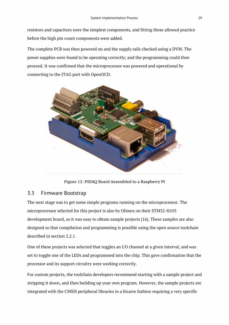
The components were ordered once the bare PCB was returned from the manufacturer. The
PCB components were then soldered on by hand over the course of an afternoon. This
process went smoothly despite a lack of experience with surface mount assembly. The
System Implementation Process 29
resistors and capacitors were the simplest components, and fitting these allowed practice
before the high pin count components were added.
The complete PCB was then powered on and the supply rails checked using a DVM. The
power supplies were found to be operating correctly; and the programming could then
proceed. It was confirmed that the microprocessor was powered and operational by
connecting to the JTAG port with OpenOCD.
Figure 12: PiDAQ Board Assembled to a Raspberry Pi
3.3 Firmware Bootstrap
The next stage was to get some simple programs running on the microprocessor. The
microprocessor selected for this project is also by Olimex on their STM32-H103
development board, so it was easy to obtain sample projects [16]. These samples are also
designed so that compilation and programming is possible using the open source toolchain
described in section 2.2.1.
One of these projects was selected that toggles an I/O channel at a given interval, and was
set to toggle one of the LEDs and programmed into the chip. This gave confirmation that the
processor and its support circuitry were working correctly.
For custom projects, the toolchain developers recommend starting with a sample project and
stripping it down, and then building up your own program. However, the sample projects are
integrated with the CMSIS peripheral libraries in a bizarre fashion requiring a very specific

30 Raspberry Pi for Data Acquisition
file and folder hierarchy to be maintained around the program code. They also use a
different build system to the one built into Eclipse. Creating a from-scratch project that
would not have any external dependencies was therefore preferable.
After some experimentation and trial and error an Eclipse project was created that used the
linker script from a sample project, but had otherwise come from a clean slate. This involved
detailed examination of the compiler and linker flags used by the samples to determine
which were necessary, and then the translation of these into Eclipse’s build system. With
this complete, there was a firm foundation on which to build the final software.
3.4 Version Control
In keeping with good software engineering practice, the source code for the project was now
placed under the Git version control system [17]. While designed for collaboration, even
when a single developer is working on the project version control provides many
advantages. It allows changes to files to be tracked so the thought process behind
implementation can be followed. In the event of regressions, it is easy to roll back to
previously working programs. The distributed nature of Git ensured the code was backed up
continuously, and allowed development to move between computers easily. Branches
allowed experimentation while concurrently working on mainstream code.
3.5 Raspberry Pi Operating System
The system was built on the best supported Raspberry Pi operating system, the Raspbian
derivative of Debian [18]. The base operating system required some configuration before the
PiDAQ could be used:
1. The SPI driver was enabled by modifying the module blacklist file
2. The kernel configuration was changed so that the serial port was not used for Linux
status messages and was under the full control of the user
3. A udev rule file was created to allow non-root users to access the spidev interface
4. The relevant Python libraries were installed
It is worth noting that a recent version of Raspbian is required for SPI support. The
Raspberry Pi used on this project was kept at the latest versions of packages and kernel
throughout.

System Implementation Process 31
3.6 Peripheral Configuration
The first peripherals to be configured were the timers. The SysTick timer was configured to
provide a ‘watchdog’ LED, set to blink continuously while the processor was running. A
normal timer peripheral was then configured to trigger events for use in testing the rest of
the system.
A mistake in the PCB design was discovered at this point. The silk screen legend labels the
LEDs incorrectly: the LED labelled as PB0 is in fact connected to PB1, and vice versa.
The next stage was to configure and test the communication peripherals. Example code for
performing this task was found in the sample projects and used as inspiration for this stage.
The serial interface was brought up first as it was simpler to use on both ends of the link.
The PiDAQ was configured to emit a stream of characters, which were detected on the
Raspberry Pi by a built-in terminal application.
At this stage an error in the timing was noticed – the values used in the timers did not
generate the intervals that were expected. Since these must be calculated in terms of the
microprocessor’s clock frequency it was implied that the oscillator was not configured
correctly, but the serial interface was clearly working at the correct baud rate as the data was
passing through without error.
Examining the source code of the CMSIS library showed that the serial peripheral library was
using a routine to obtain the system’s current clock frequency before calculating baud rate,
whereas the timer library was using a constant set at compile time. Using the debugger to
inspect the result of the routine used in the serial library showed the clock frequency was 9
times slower than anticipated.
Attaching breakpoints in the microprocessor’s start up routines then showed that the start-
up of the external oscillator was timing out, and that the system was instead running on its
slow internal oscillator. Examining the circuit design (Figure 21, page 45) showed that the
resistor R14 had been placed incorrectly, in parallel with the crystal rather than in series
with it. Modifying the circuit to place this in series would have been difficult, but removing
it fixed the problem and the clock was shown to then start up correctly. The series resistance
(REXT in Figure 4, page 14) is not critical to correct operation.
32 Raspberry Pi for Data Acquisition
An example program in C (spidev_test.c) is provided along with the documentation for spidev
[13] to test the SPI device using a loopback connection (MOSI connected to MISO). This
program was successfully compiled and run on the Raspberry Pi. The PiDAQ was connected,
and a basic test firmware was created to send a stream of data. This worked successfully
when run with the spidev test program.
A common mistake made when configuring peripheral was not enabling the peripheral’s
clock. Unlike the microprocessors worked with previously, the STM32 requires this extra
step, which is obscured in the example programs. With the clock not activated, all CMSIS
API calls return successfully, but if examined in the debugger the register values they are
affecting are not actually modified.
The next task was to interface the spidev driver to Python. For this some candidate modules
were found that were written in C and were based on the test program distributed with the
driver. One such module was written by the team responsible for the Pi-Face, since this
board used SPI I/O expanders [19]. This was selected as the best candidate for use with the
PiDAQ, and was modified to remove some Pi-Face specific functionality. Running the same
test firmware showed that the module was working adequately.
3.7 Increasing the Sample Rate
To test the system’s communications, it was desirable to run the PiDAQ at a high sample
rate, but with predictable data such that a test program would be able to detect any
corruption. The desire for this marked the first major restructuring of the embedded code,
with the code split into modules for the different peripherals and converted to being
interrupt driven. The buffer pool was also implemented at this stage. It was then possible to
write a routine that filled the buffers on the device with sequentially increasing samples.
Such a pattern allows errors to be easily detected throughout the system. This system was
implemented using the same timers and DMA configuration that would be used for analogue
sampling, so that minimal work would be involved in changing from one to the other.
This mock data allowed the Python SPI module to be tested, and then a source for the
storage engine was implemented that worked with the data from the SPI bus.

System Implementation Process 33
With data now coming into the storage engine, it was time to increase the data rate and
pressure test the various buffering schemes. It is at this stage that the project stalled, with a
large amount of development effort spent in improving performance in this area.
After raising the rate of data generation to 10 kS/s, the SPI test program began to fail. The
PiDAQ was generating data faster than the Raspberry Pi could request it. Simply increasing
the size of the buffers would not resolve the issue, only delay its appearance.
The first goal was to get the test program running fast enough to read all the data, even if no
further processing was occurring. This program used the protocol as designed, periodically
transferring a single byte to check for a header. If the byte was non-zero, then samples were
available and that many further bytes were transferred. Removing the interval between
polling (replacing it with a tight loop) allowed the test program to retrieve data quick
enough, and counting the loop iterations between groups of samples gave an indication of
how close to overflow the program was. This iteration counter was giving values in the
hundreds in the test program.
This logic was then implemented in the hardware abstraction module, but overflow still
occurred. To remove one possible cause it was decided to eliminate the networking between
the hardware abstraction module and the storage engine, integrating the code directly. At
this stage the system could process the samples, but with very little leeway. The iteration
counter was giving results in single digits.
The decision was then taken to move the PiDAQ interface into a C Python module. Python’s
multithreading implementation is much slower than C’s, so switching into the source thread
for each loop iteration had a high cost. Moving the tight loop into C allowed around 10 times
more iterations between groups of samples, but this was still not robust enough.
The next step taken was to change the looping strategy. The SPI module on the Raspberry Pi
uses DMA such that while a transfer is occurring the processor is free to perform other tasks.
To exploit this, the loop was modified to transfer a much larger number of bytes, then to
search through the transferred bytes for message headers, rather than transferring many
small amounts. This provided close to adequate throughput for samples. The final stage was
to move this operation into a C thread which could run continuously, creating a buffer of
samples internal to the C module which could be implemented efficiently and periodically

34 Raspberry Pi for Data Acquisition
emptied by a call into the module from Python. The size of the larger transfer was optimised
to provide a good trade-off between time spent performing DMA, and time spent searching
through the transferred bytes for headers.
This represented the most efficient scheme for performing the SPI transactions available
without implementing a custom driver. Unfortunately while the storage engine could
manage this data throughput in memory, usable recording time at this rate was limited to a
few seconds (the size of the block pool in memory) as the write speed of the SD card in use
with the Raspberry Pi was too slow.
3.8 16-bit Transfers
Issues also presented themselves around the 16-bit word size. The early testing was
conducted using 8-bit SPI words, before a later change to 16-bit. At this point it was
discovered that despite the Raspberry Pi and the microprocessor using the same endianness
(byte ordering of multi-byte quantities) the bytes coming out of the spidev interface were
reversed. The problem was temporarily fixed by swapping the byte order in the interface
module.
The true source of this problem would not be revealed until a later time, when an update to
the Raspberry Pi’s SPI driver caused it to display errors that occurred when the device was
being configured. The code to perform transfers started causing an error, and this was
eventually tracked down to a problem setting the word size to 16 bits. Further research
revealed that the Raspberry Pi’s SPI driver was not in fact capable of 16 bit word transfers,
and was only functioning because a 16 bit transfer is identical at a low level to two
consecutive 8 bit transfers, which was what the device was performing. The processor’s little
endian architecture then led the bytes to be swapped, as the 16 bit word from the
microprocessor was transferred with the most significant byte first, but a little endian
processor stores the least significant byte first.
As this was discovered at a late stage in development the work-around was left in place. A
full fix would require reconfiguring the SPI peripheral in the microprocessor.
3.9 Analogue Sampling
Once the sample ‘plumbing’ was complete the ADC module could be enabled. Configuring
the ADC module itself was fairly simple, and the ADC in scan mode filled the buffer with

System Implementation Process 35
samples in the interleaved pattern as specified in the protocol. More complicated was
arranging for the timer to trigger the ADC conversion at the sampling rate. The
documentation for the microprocessor is particularly thin on this point, but one of the
example programs provided a pattern to follow. The capture/compare module of the
triggering timer must be configured in PWM mode for the trigger signal to work correctly.
3.10 User Interface
With the sampling now working sufficiently well, the next step was to work on improving
the user interface. When live streaming at tens of thousands of samples per second the
amount of data involved is very large, it was found that the designed method of querying the
storage engine for data represented too much overhead and was causing the storage engine
to stall. As a solution to this, the live streaming was re-implemented using a subscription
pattern and UDP streaming of the raw data.
In the new method, the controller sends a command to register itself as a recipient of live
streaming, and the storage engine then sends the samples to the controller as it receives
them without any polling. This drastically reduced the overhead on the storage engine.
The next issue was with the display of the data. At a 10 kHz sampling rate, showing a few
seconds of previous data involves displaying tens of thousands of data points. It transpired
that even making use of the animation features of matplotlib to perform a partial refresh, it
could not display this amount of data at a sensible frame rate.
Initially this problem was attacked by down-sampling the data before passing it to
matplotlib – a window 500 pixels wide could never show all the detail present in 50000
samples. This allowed the frame rate to reach a reasonable level of around 30 fps on a
windows laptop, but the end goal was to be able to run the entire system on the Raspberry
Pi. With down-sampling and while also running the storage engine the Raspberry Pi could
only manage a frame every few seconds due to its far lower processing power.
The solution to this was to switch to a lighter-weight plotting library. wxWidgets includes a
library that is intrinsically better integrated with the toolkit, and provides a good trade-off
between reducing functionality and improving performance. For the simple application of
live data view it was more than sufficient, and allowed the controller to achieve sensible
frame rates on the Raspberry Pi.
36 Raspberry Pi for Data Acquisition
3.11 Digital I/O
The implementation of the digital interface was performed at a later stage in development
as it was a non-critical feature. Implementation of the protocol controlling the interface was
fairly straightforward, but during this process two errors in the hardware design were
revealed, one minor and one serious.
Because of a strange ordering on the ST-supplied schematic symbol for the microprocessor,
the 7th and 8th digital lines were connected to each other’s pins on the microprocessor. This
would be relatively trivial to work around in software (see pins PC6 and PC7 in schematic,
Figure 21 on page 45).
The more serious flaw was with the connection of the level-shifter chip. Because this block
was designed with unclear nomenclature for the schematic ports (in and out, when the block
is bidirectional), on the high level schematic (Figure 15, page 42) the 5V side was connected
to the microprocessor and the 3.3V side to the external contacts (compare with the port
labels in Figure 18, page 43). This error was then carried through the rest of the design and
build process. The impact of this was that four of the digital pins (0-3) could not be used as
inputs as the corresponding microprocessor pins are not 5V tolerant, and the outputs only
achieve a level of 3.3V. Solving this problem would require a new revision of the PCB to be
made, and since the error was discovered late, and relates to a minor feature of the board, it
was not worth the time and expense to rectify the problem.
3.12 Final User Interface
The final iteration of the user interface was split into two parts. The controller displayed live
data and allowed sessions to be started and stopped. A command line application was
created to display recorded data and to export this to CSV. Due to time constraints the
second application was designed to work with local copies of the data only rather than
operating across the network.

Testing 37
4 Testing For a final test of the analogue inputs, the system was connected to another microcontroller
generating a sine wave using its analogue output capabilities.
Figure 13: Live View of Generated Sine Wave
Figure 13 shows the controller GUI displaying a 1 Hz sine wave captured at 5 kS/s. The x-axis
is in samples and the y-axis is the output count up a full scale of 4096.
This capture rate represented the performance ceiling of data acquisition and display. The
generating microcontroller had an output range of 3.3V, which should have corresponded to
a reading of 819. The actual reading was 762. The attenuator circuit was introducing an
offset equivalent to 0.22 V on the input, leading to the clipping visible at the extreme low-
end of the graph. The cause of this offset thought to be within the generator circuit, as it is
not present when the analogue inputs are grounded.
The sine wave was reproduced correctly in terms of the time axis, with no discontinuities,
showing that the system was not dropping or corrupting any data.
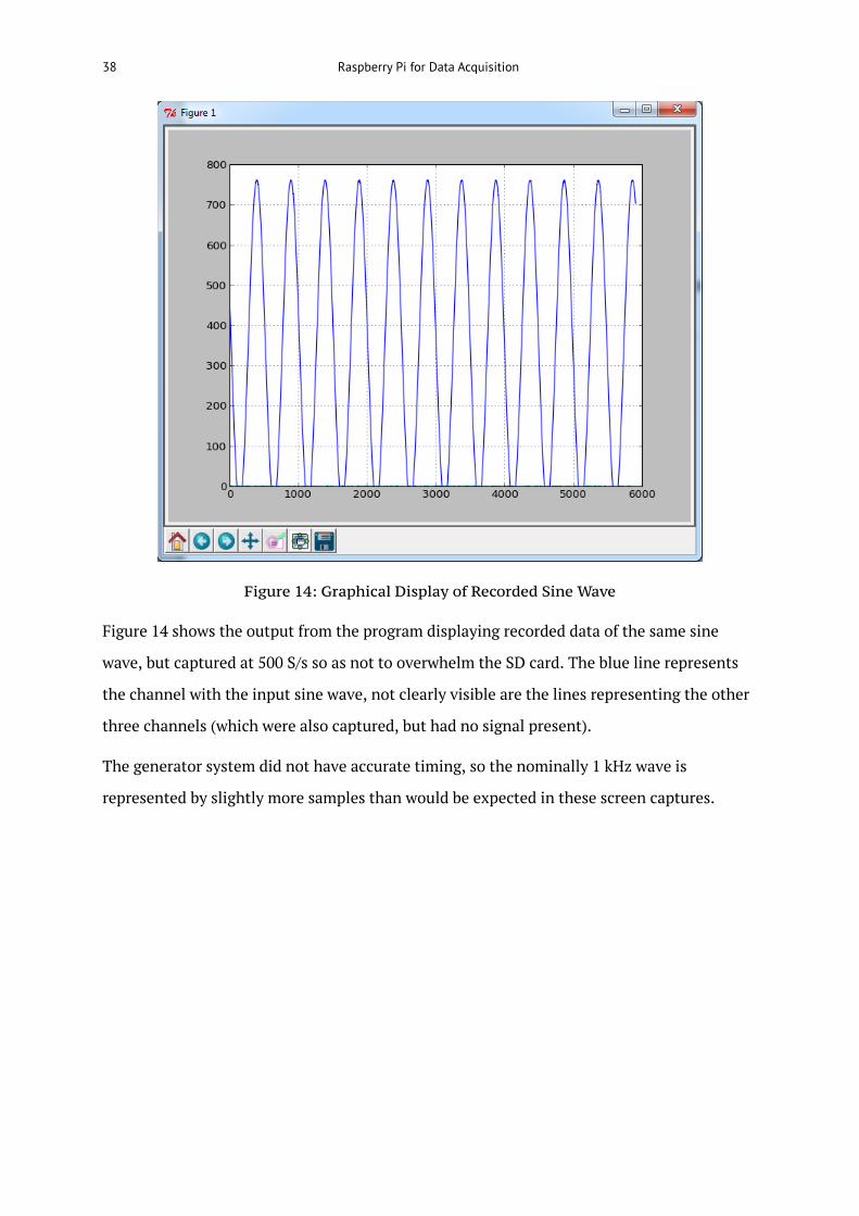
38 Raspberry Pi for Data Acquisition
Figure 14: Graphical Display of Recorded Sine Wave
Figure 14 shows the output from the program displaying recorded data of the same sine
wave, but captured at 500 S/s so as not to overwhelm the SD card. The blue line represents
the channel with the input sine wave, not clearly visible are the lines representing the other
three channels (which were also captured, but had no signal present).
The generator system did not have accurate timing, so the nominally 1 kHz wave is
represented by slightly more samples than would be expected in these screen captures.
Conclusions 39
5 Conclusions As is often the case with design projects, the parts that were expected to be easy were found
to be difficult, and this meant that the project did not achieve all that it set out to. In
particular, at the planning stage the capabilities of the Raspberry Pi to handle the quantities
of data involved were overestimated, and a lot more thought should have been given to
making the system efficient, both in terms of memory and processing time.
With regard to the milestones in the Project Plan, section 1.4 above, the PiDAQ Mk I was
completed two weeks late due to delays in the ordering of components. The System Software
then took considerably longer to develop than anticipated, consuming the rest of Lent term
and leaving no time to design a PiDAQ Mk II. The User Software is more rudimentary than
originally envisioned, its development time being likewise limited.
It was decided to drop the PiDAQ Mk II from the project as the benefits from having a direct
thermocouple interface were small. At the time the errors in the digital I/O circuitry had not
been discovered, if they had been then there would have been a greater impetus to revise the
PCB. The PiDAQ Mk I, however, showed that the chosen architecture was suitable for the
task at hand, the microprocessor working as desired from an early stage.
The system that has been built can achieve a 5 kS/s rate on four channels, which is still fast
enough for a large variety of laboratory applications. In the process of achieving this rate a
lot has been learned about the complexities of a DAQ system and in particular how the
environment of the Raspberry Pi impacts on the solution chosen.
For example, the flexibility of Linux and the presence of the GPIO header allowed the SPI
communications to be implemented without writing a driver, but this made designing the
interface to Python more technically challenging. The lower speed and single core processor
of the Raspberry Pi require adjusting the mind-set of the programmer as, if you expect
reasonable performance, the Raspberry Pi cannot be programmed as casually as a quad-core
desktop computer. Likewise with the network streaming of data – at high data rates the
overhead of the protocol became very significant and the naïve design had to be replaced.
Something as small as the write speed of the SD card in the Raspberry Pi presented a
bottleneck which was not initially envisioned.
40 Raspberry Pi for Data Acquisition
5.1 Future Work
Recent innovations in the Raspberry Pi ecosystem, such as developments with the
alternative PyPy Python runtime [20], could give a significant performance boost to the
Python storage engine without any rewriting. The possibility of writing a pure-C driver for
the PiDAQ should also be considered, this could be built from the existing interface module
and provide more reliable throughput from the PiDAQ to the Raspberry Pi. Linux on ARM is
maturing constantly and will only continue to grow in popularity, and the tools for
development are maturing alongside it.
There is ample scope for adding electronic functionality, such as thermocouple interfaces,
with a PiDAQ Mk II. The Mk I merely showed that analogue data capture at high data rates
was possible, rather than leaning towards any particular application. Making a distributed
DAQ system out of several linked Raspberry Pi’s could form a project in its own right.
The project in its final form still represents a capable platform for data acquisition, albeit a
little rough around the edges. The key functionality is there, and there is a clear pathway for
achieving the full potential of the Raspberry Pi as a Data Acquisition system.
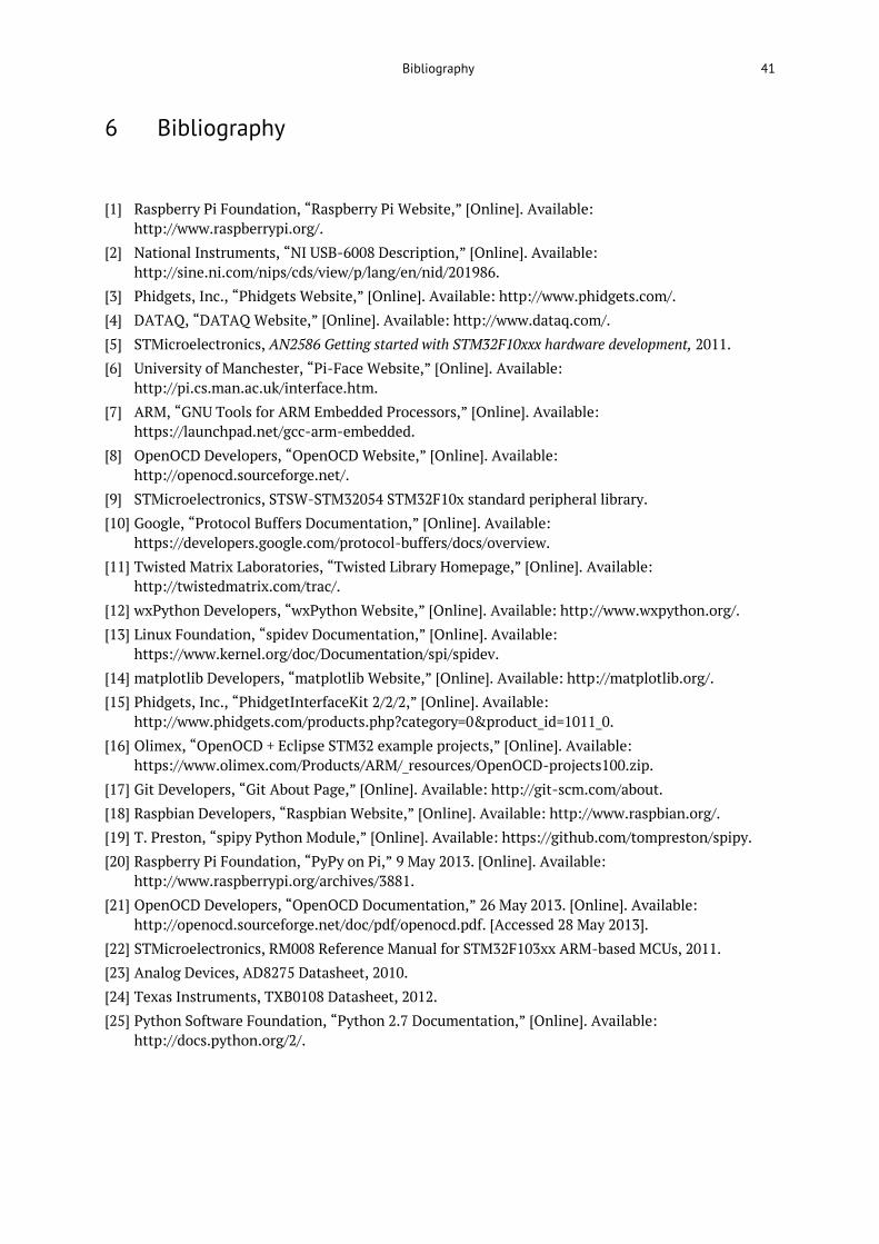
Bibliography 41
6 Bibliography
[1] Raspberry Pi Foundation, “Raspberry Pi Website,” [Online]. Available: http://www.raspberrypi.org/.
[2] National Instruments, “NI USB-6008 Description,” [Online]. Available: http://sine.ni.com/nips/cds/view/p/lang/en/nid/201986.
[3] Phidgets, Inc., “Phidgets Website,” [Online]. Available: http://www.phidgets.com/. [4] DATAQ, “DATAQ Website,” [Online]. Available: http://www.dataq.com/. [5] STMicroelectronics, AN2586 Getting started with STM32F10xxx hardware development, 2011. [6] University of Manchester, “Pi-Face Website,” [Online]. Available:
http://pi.cs.man.ac.uk/interface.htm. [7] ARM, “GNU Tools for ARM Embedded Processors,” [Online]. Available:
https://launchpad.net/gcc-arm-embedded. [8] OpenOCD Developers, “OpenOCD Website,” [Online]. Available:
http://openocd.sourceforge.net/. [9] STMicroelectronics, STSW-STM32054 STM32F10x standard peripheral library. [10] Google, “Protocol Buffers Documentation,” [Online]. Available:
https://developers.google.com/protocol-buffers/docs/overview. [11] Twisted Matrix Laboratories, “Twisted Library Homepage,” [Online]. Available:
http://twistedmatrix.com/trac/. [12] wxPython Developers, “wxPython Website,” [Online]. Available: http://www.wxpython.org/. [13] Linux Foundation, “spidev Documentation,” [Online]. Available:
https://www.kernel.org/doc/Documentation/spi/spidev. [14] matplotlib Developers, “matplotlib Website,” [Online]. Available: http://matplotlib.org/. [15] Phidgets, Inc., “PhidgetInterfaceKit 2/2/2,” [Online]. Available:
http://www.phidgets.com/products.php?category=0&product_id=1011_0. [16] Olimex, “OpenOCD + Eclipse STM32 example projects,” [Online]. Available:
https://www.olimex.com/Products/ARM/_resources/OpenOCD-projects100.zip. [17] Git Developers, “Git About Page,” [Online]. Available: http://git-scm.com/about. [18] Raspbian Developers, “Raspbian Website,” [Online]. Available: http://www.raspbian.org/. [19] T. Preston, “spipy Python Module,” [Online]. Available: https://github.com/tompreston/spipy. [20] Raspberry Pi Foundation, “PyPy on Pi,” 9 May 2013. [Online]. Available:
http://www.raspberrypi.org/archives/3881. [21] OpenOCD Developers, “OpenOCD Documentation,” 26 May 2013. [Online]. Available:
http://openocd.sourceforge.net/doc/pdf/openocd.pdf. [Accessed 28 May 2013]. [22] STMicroelectronics, RM008 Reference Manual for STM32F103xx ARM-based MCUs, 2011. [23] Analog Devices, AD8275 Datasheet, 2010. [24] Texas Instruments, TXB0108 Datasheet, 2012. [25] Python Software Foundation, “Python 2.7 Documentation,” [Online]. Available:
http://docs.python.org/2/.
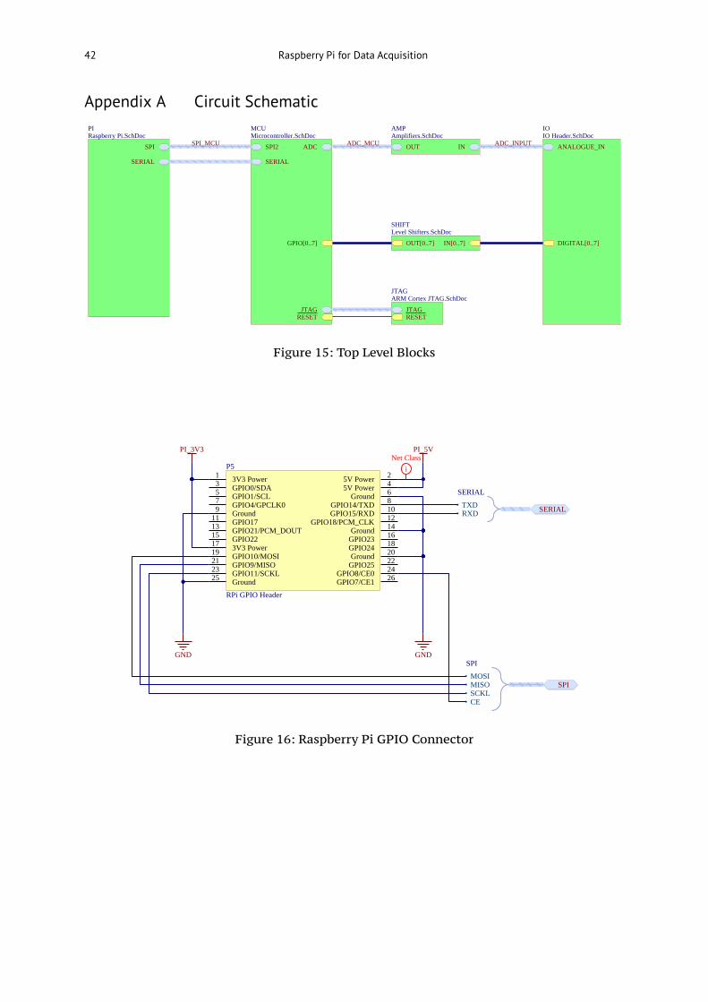
42 Raspberry Pi for Data Acquisition
Appendix A Circuit Schematic
Figure 15: Top Level Blocks
Figure 16: Raspberry Pi GPIO Connector
SPI
SERIAL
PIRaspberry Pi.SchDoc
SPI2
GPIO[0..7]
JTAG
ADC
RESET
SERIAL
MCUMicrocontroller.SchDoc
DIGITAL[0..7]
ANALOGUE_IN
IOIO Header.SchDoc
OUT IN
AMPAmplifiers.SchDoc
IN[0..7]OUT[0..7]
SHIFTLevel Shifters.SchDoc
SPI_MCU ADC_MCU ADC_INPUT
JTAGRESET
JTAGARM Cortex JTAG.SchDoc
3V3 Power1
5V Power2
GPIO0/SDA3
5V Power4
GPIO1/SCL5
Ground6
GPIO4/GPCLK07
GPIO14/TXD8
Ground9
GPIO15/RXD10
GPIO1711
GPIO18/PCM_CLK12
GPIO21/PCM_DOUT13
Ground14
GPIO2215
GPIO2316
3V3 Power17
GPIO2418
GPIO10/MOSI19
Ground20
GPIO9/MISO21
GPIO2522
GPIO11/SCKL23
GPIO8/CE024
Ground25
GPIO7/CE126
P5
RPi GPIO Header
GNDGND
PI_3V3 PI_5V
MOSIMISOSCKLCE
SPI
SPI
i
Net Class
TXDRXD
SERIAL
SERIAL
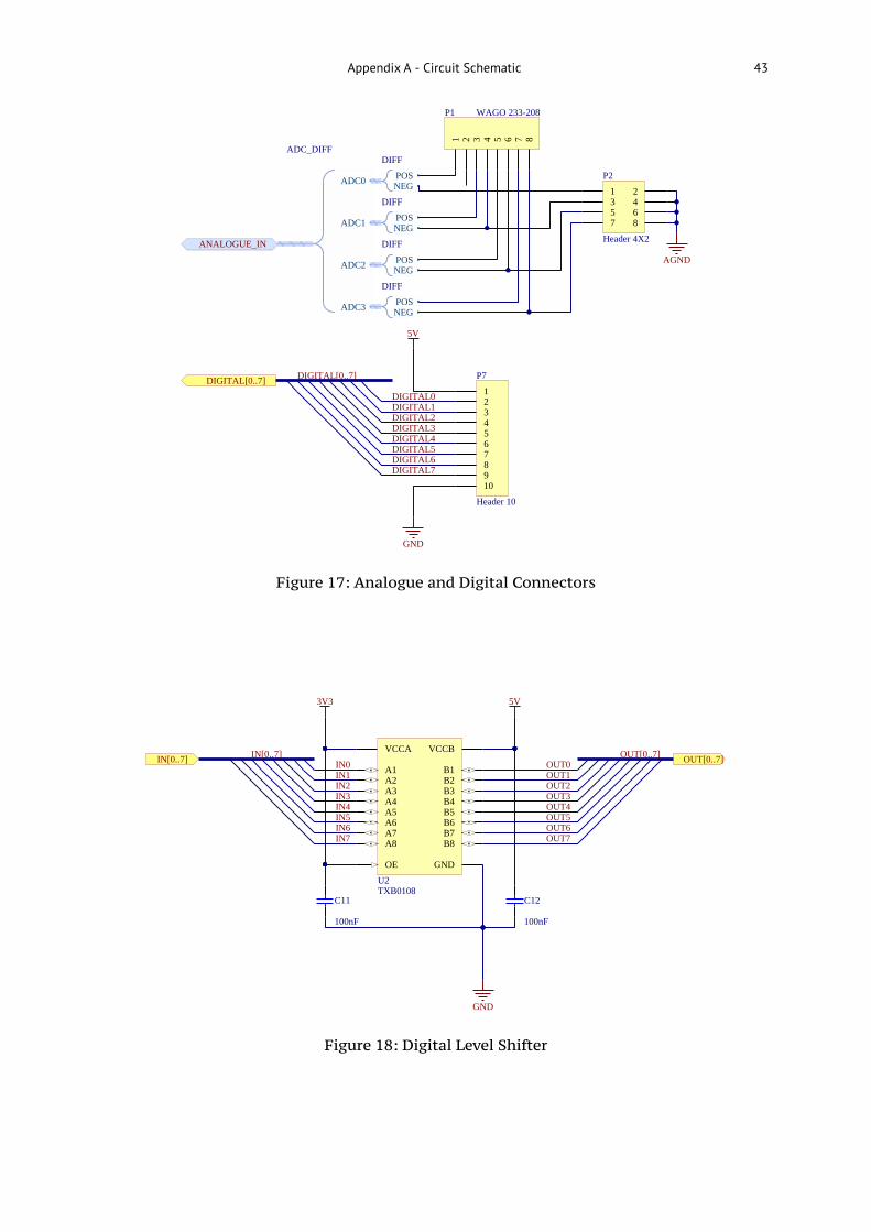
Appendix A - Circuit Schematic 43
Figure 17: Analogue and Digital Connectors
Figure 18: Digital Level Shifter
DIGITAL[0..7]12345678910
P7
Header 10
5V
GND
DIGITAL0
DIGITAL[0..7]
ADC0
ADC1
ADC2
ADC3
ADC_DIFF
ANALOGUE_IN
1 2 3 4 5 6 7 8
P1 WAGO 233-208
DIGITAL1DIGITAL2DIGITAL3DIGITAL4DIGITAL5DIGITAL6DIGITAL7
POSNEG
DIFF
POSNEG
DIFF
POSNEG
DIFF
POSNEG
DIFF
1 23 45 67 8
P2
Header 4X2
AGND
IN[0..7] OUT[0..7]VCCA
A1A2A3A4A5A6A7A8
OE GND
B8B7B6B5B4B3B2
VCCB
B1
U2TXB0108
3V3 5V
GND
IN[0..7] OUT[0..7]IN0IN1IN2IN3IN4IN5IN6IN7
OUT0OUT1OUT2OUT3OUT4OUT5OUT6OUT7
100nF
C11
100nF
C12

44 Raspberry Pi for Data Acquisition
Figure 19: JTAG Connector
Figure 20: Power Supplies
3V3
10KR5
10KR6
TDI
TMSTCK
TDO
JTAG
JTAG
RESET
TMSTCKTDOTDInRST
3V3
GND
TMSTCK
nRST
TDITDO
10KR7
10KR8
10KR9
1 23 45 67 89 10
P6
HEADER 10WAY DUAL
GND1
VOUT2
VIN3
U3
MCP1700T-3302E/TT
3V3
GND
PI_5V
GND1
VOUT2
VIN3
U4
MCP1700T-3302E/TT
A3V3
AGND
5V
NT1
GND AGND
1uFC13
1uFC14
1uFC15
1uFC16
i
Net Class
i
Net Class
i
Net Class
i
Net Class
i
Net Class
D3
GND
100RR14
+Vin
-Vin
+Vout
-Vout
U6
MER1S0509SC
PI_5V 9V
GND
i
Net Class
i
Net Class
VIN3
2
VOUT1
GND
1467762U7
L78L05ABUTR
AGND
5V
i
Net Class
100nF
C19
330nF
C18
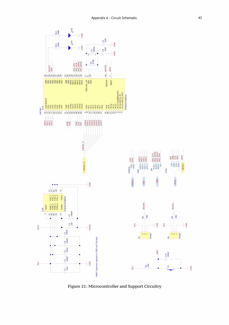
Appendix A - Circuit Schematic 45
Figure 21: Microcontroller and Support Circuitry
GP
IO[0
..7
]
BO
OT
06
0
NR
ST
7
PD
0-O
SC
_IN
5
PD
16
PA
0-W
KU
P1
4
PA
11
5
PA
21
6
PA
31
7
PA
42
0
PA
52
1
PA
62
2
PA
72
3
PA
84
1
PA
94
2
PA
10
43
PA
11
44
PA
12
45
PA
13
46
PA
14
49
PA
15
50
PB
02
6
PB
12
7
PB
22
8
PB
35
5
PB
45
6
PB
55
7
PB
65
8
PB
75
9
PB
86
1
PB
96
2
PB
10
29
PB
11
30
PB
12
33
PB
13
34
PB
14
35
PB
15
36
PC
08
PC
19
PC
21
0
PC
31
1
PC
42
4
PC
52
5
PC
73
8
PC
63
7
PC
83
9
PC
94
0
PC
10
51
PC
11
52
PC
12
53
PC
13-T
AM
PE
R-R
TC
2
PC
14-O
SC
32_IN
3
PC
15-O
SC
32_O
UT
4
PD
25
4
14
47
64
0U
1A
ST
M32F
103
RB
T6
VB
AT
1
VD
D_
13
2
VD
D_
24
8
VD
D_
36
4
VD
D_
41
9
VD
DA
13
VS
S_
13
1
VS
S_
24
7
VS
S_
36
3
VS
S_
41
8
VS
SA
12
U1
B
ST
M32F
103
RB
T6
10
0n
FC
21
00
nF
C3
10
0n
FC
41
00
nF
C5
GN
DG
ND
10
0n
FC
71
uF
C6
AG
ND
3V
3
TD
IT
MS
TC
KT
DO
JTA
G1
00
nF
C10
S110
KR
3
3V
3
GN
D
nR
ST
nR
ST
nR
ST
JTA
G
CE
MIS
OM
OS
IS
CK
LS
PI
SP
I2
BO
OT
0
BO
OT
1
123
P3
Jum
per
10
K
R2
3V
3
GN
D
123
P4
Jum
per
10
K
R4
3V
3
GN
D
BO
OT
0
BO
OT
1
8M
Hz
13
Y1
47
0R
R1
15
pF
C9
15
pF
C8
GN
DG
ND
SP
I2_S
CK
SP
I2_M
OS
IS
PI2
_M
ISO
SP
I2_N
SS
SP
I2_N
SS
SP
I2_S
CK
SP
I2_M
ISO
SP
I2_M
OS
I
TM
ST
CK
TD
I
TD
O
TD
OT
CK
TM
ST
DI
AD
C0
AD
C1
AD
C2
AD
C3
AD
CA
DC
0A
DC
1A
DC
2A
DC
3
AD
C0
AD
C1
AD
C2
AD
C3
AD
C
GP
IO0
GP
IO1
GP
IO2
GP
IO3
GP
IO4
GP
IO5
GP
IO6
GP
IO7
GP
IO[0
..7
]
10
uF
C1
10
0n
F C
apac
ito
rs a
dja
cen
t to
VD
D a
nd
VS
S p
ins
A3
V3
RE
SE
T
RX
DT
XD
SE
RIA
L
SE
RIA
LT
XD
RX
D
RX
DT
XD
D1
D2
GN
DG
ND
10
0R
R12
10
0R
R13

46 Raspberry Pi for Data Acquisition
Figure 22: Analogue Interface Amplifiers
ADC0ADC1ADC2ADC3
ADC_DIFF
IN
ADC0ADC1ADC2ADC3
ADC
OUTIN OUT
ADC_SHIFT0ADC Shift.schdoc
IN OUT
ADC_SHIFT1ADC Shift.schdoc
IN OUT
ADC_SHIFT2ADC Shift.schdoc
IN OUT
ADC_SHIFT3ADC Shift.schdoc
OUT
-IN2
+IN3
-Vs4
+Vs7
Sense5
Out6
Ref11
Ref28
U5
AD8275
5V
AGND
100nFC17
10KR10
47KR11
AGND
NEGPOS
DIFF
IN
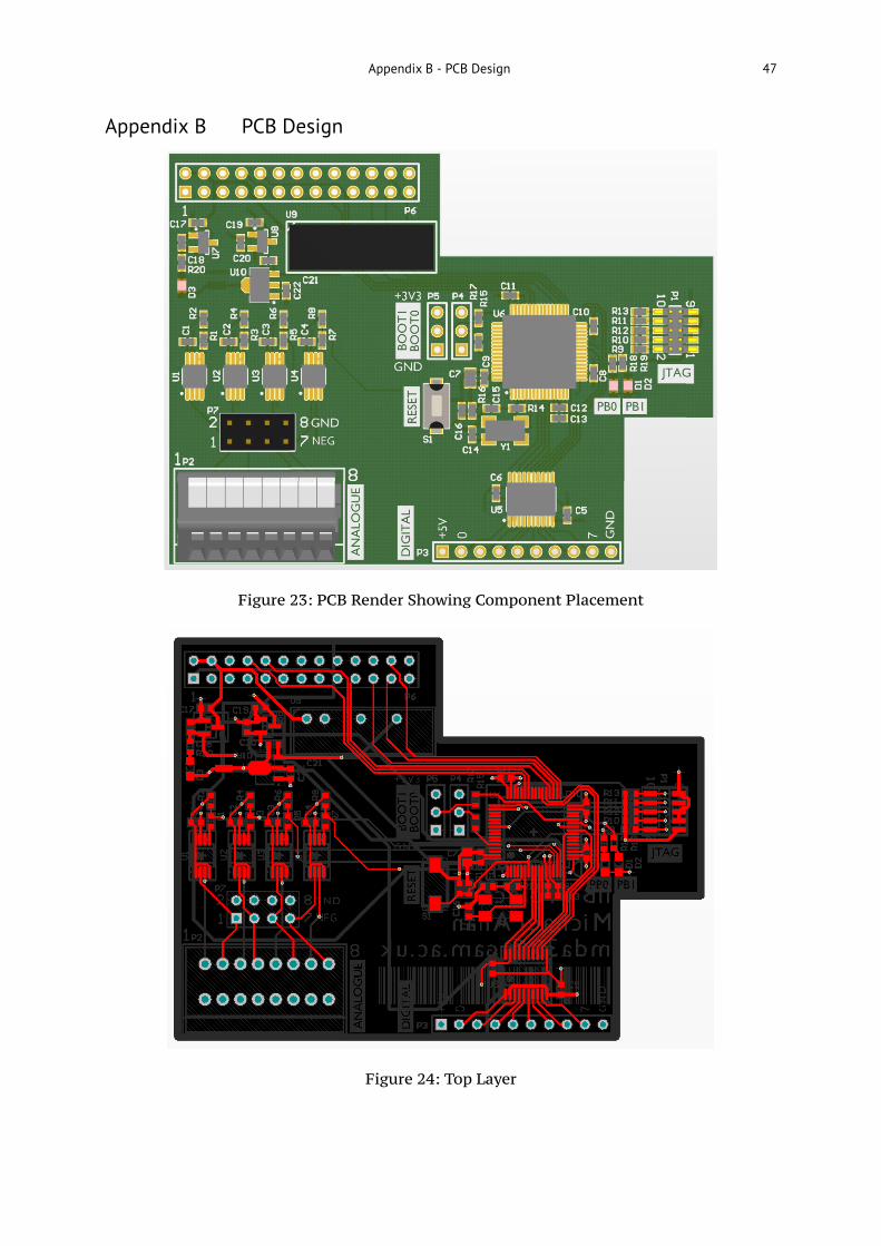
Appendix B - PCB Design 47
Appendix B PCB Design
Figure 23: PCB Render Showing Component Placement
Figure 24: Top Layer
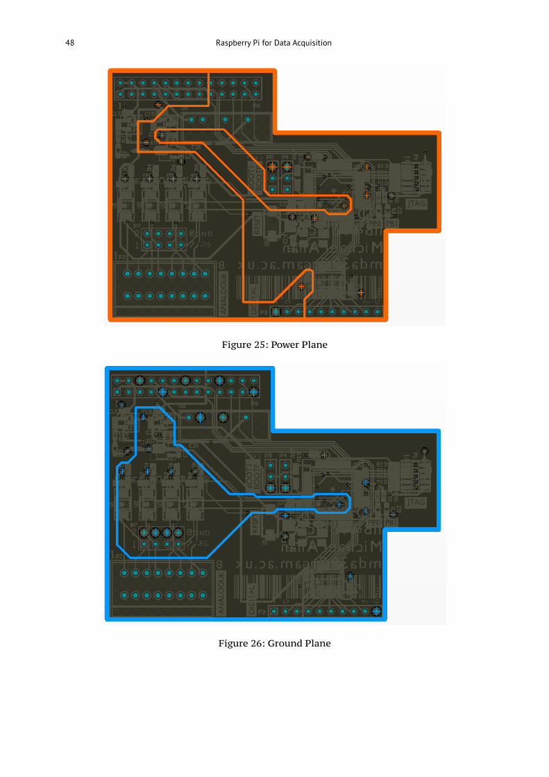
48 Raspberry Pi for Data Acquisition
Figure 25: Power Plane
Figure 26: Ground Plane

Appendix B - PCB Design 49
Figure 27: Bottom Layer

50 Raspberry Pi for Data Acquisition
Appendix C Risk Assessment Retrospective
The main hazards associated with the project were accounted for in the risk assessment,
namely extended use of a computer and soldering.
With regards to computer use, while the department provided a suitable workstation, the
use of hardware and software not available within the department to design and program the
PCB meant that the vast majority of the work was carried out in a college room, where the
facilities provided were less than ideal, and there is no scope for improvement as the
furniture is supplied by college (and this is the only furniture permitted to be used). It may
be worth considering either providing a more secure area within the department (allowing
the proprietary hardware to be left there and work to be carried out there) or pressuring
colleges to provide more suitable working areas within student’s study bedrooms.
The second significant risk, soldering, was correctly judged in the assessment. The work area
(Design and Project Room), while not ideal, was sufficiently ventilated for the brief period of
soldering that occurred during the project. Since this project was conducted under the
auspices of Division A, a workspace in the EIETL was not offered, but given the small
amount of relevant work done it was not requested either. In future the situation could be
improved by pre-emptively making EIETL space and equipment available to all students
with electronics elements to their project on an ad-hoc basis.