rca bts-1a stereo subcarrier generator - hallikainenbh.hallikainen.org/wiki/uploads/rcabts1a.pdf ·...
TRANSCRIPT

\
Broadcast Equipment
BTS-1 A Stereo Subcarrier Generator
ES-560202
IB-30297

-1-
Broadcast Equipment
Instructions
BTS-1 A
Stereo Subcarrier Generator
ES-560202
COmmUniCatiOnS Systems Division/Front and Cooper Streets/Camden, New Jersey, U.S.A. 08102
DL763M IB-30297
2
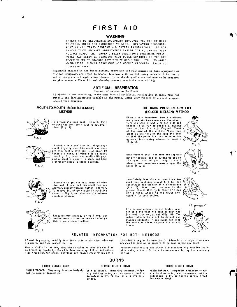
FIRST AID WARNING
OPERATION OF ELECTRONIC EQUIPMENT INVOLVES THE USE OF HIGH VOLTAGES WHICH ARE DANGEROUS TO LIFE. OPERATING PERSONNEL MUST AT ALL TIMES OBSERVE ALL SAFETY REGULATIONS. DO NOT CHANGE TUBES OR MAKE ADJUSTMENTS INSIDE THE EQUIPMENT WITH VOLTAGE SUPPLY ON. UNDER CERTAIN CONDITIONS DANGEROUS POTEN- TIALS MAY EXIST IN CIRCUITS WITH POWER CONTROLS IN THE OFF POSITION DUE TO CHARGES RETAINED BY CAPACITORS. ETC. TO AVOID CASUALTIES, ALWAYS DISCHARGE AND GROUND CIRCUITS PRIOR TO TOUCHING THEM.
Personnel engaged in the installation, operation and.maintenance of this equip,ment or similar equipment are urged to become familiar with the following rules both in theorV and in the practiwal application thereof. It is the duty of every radioman to be prepared to give adequate First Aid and thereby prevent avoidable loss of life.
ARTIFICIAL RESPIRATION (Courtesy of the American Red Cross)
If victim is not breathing, begin snme form of artificial respiration at once. Wipe nnt quickly any foreign matter visible in the month, using your fingers or a cloth wrapped around your fingers.
MOUTH-TO-MOUTH (MOUTH-TO-NOSE) METtiOD
Fig. 1 Fig. 1
Fig. 2
Fig. 4
If vomiting occurs, his mouth, and then
Tilt victim's head back. (Fig.1). Pull or push the jaw into a jutting-out posi- tion. (Fig. 2).
If victim is a small child, place your mouth tightly over his mo;th and nose and blow gently into his lupgs about 20 times a minute. If victim is an adult (see Fig. 3), cover the mouth with your mouth, pinch his nostrils shut. and blow vigorously about I2 times a minute.
If unable to get air into lungs of vic- tim, and if head and iaw positions are corkect, suspect foreign matter in throat, To remove it, place victim in position shown in Fig. 6, and slap sharply between shoulder blades.
Rescuers who cannot, or will not, use mouth-to-mouthormouth-to-nose technique should use a manual method.
RELATED INFORMATION FOR BOTH METHODS
quickly turn the victim on his side, wipe out reposition him.
the victim begins to breathe for himself or a physician pro- nounces him dead or he appears to be dead beyond any doubt.
When a victim is revived, keep him as quiet as possible until he is breathing regularly. Keep him from becoming chilled and other- wise treat him for shock. Continue artificial respiration until
THE BACK PRESSURE-ARM LIFT (HOLGER-NIELSEN) METHOD
Place victim face-down, bend his elbows and place his hands one upon the other, turn his head slightly to one side and extend it as far as possible, making sure that the chin is jutting out. Kneel at the head of the victim. Place your hands on the flat of the victim's back so that the palms lie just below an im- aginary line running between the armpits (Fig. 5).
Fig. 5
Rock forward until the arms are approxi- mately vertical and allow the weight of the upper part of your body to exert steady, even pressure downward upon the hands (Fig. 6).
Fig. 6
Immediately draw his arms upward and to- ward you, applying enough lift to feel resistance and tension at his shoulders (Fig. 7). Then lower the arms to the ground. Repeat this cycle about I2 times per minute, checking the mouth fre- quently for obstruction.
If a second rescuer is available, have him hold the victim's head so that the jaw continues to jut out (Fig. 8). The helper should be alert to detect any stomach cootents in the mouth and keep the mouth as clean as possible at all times.
Because respiratory and other disturbances may develop as an aftermath, a doctor's care is necessary during the recovery period.
BURNS FIRST DEGREE BURN SECOND DEGREE BURN THIRD DEGREE BURN
SKIN REDDENED. Temporary treatment-Apply SKIN BLISTERED. Temporary treatment--p- FLESH CHARRED. baking soda or Unguentine.
Temporary treatment- Ap- ply baking sode, wet compress, white ply baking soda, wet compress, white petroleum jelly, foille jelly, olive oil, petroleum jelly, or foille spray. Treat or tea. for severe shock.

--
3
TABLE OF CONTENTS
BTS-IA Stereo Subcarrier Generator
Page
LIST OF CONTENTS OF EQUIPMENTS (ES-560202) . . . . . . . . . . ......................... . . . . 4,s
TECHNICAL DATA .............................. . . . . . . ......................... . . . . . 5
TUBE COMPLEMENT ............................ . . . . . 5
DESCRIPTION .................................. ...... . . . ......................... . . . 7
General ...................................... ...... . . . . ......................... . . . 7 Circuit Description ............................ ...... . . . ......................... . . 7
Pre-emphasis .............................. ...... . . . . ......................... . . . . . 7
Matrixing ................................ ...... . . . . ......................... . . . . . 7 Matrix Inputs and Outputs ................. ...... . . ......................... . . . . 10
Filter Network ............................ ...... . ......................... . 10
Composite Signal .......................... ...... . . . . ......................... . . . . . 10
Stereo Mono Relay ........................ ...... . . . . ......................... . 13
Crystal Oscillator ......... : ................ ...... . . . . ......................... . . . . . 13
Power Supply ............................. ...... . . . ......................... . 13
Input Adapter ............................ ...... . . ......................... . . . 13
Band Pass Filter .......................... ......................... . . . 14
INSTALLATION ................................. ...... . . . . . ...... . . . . . . . 14
BTE-1OB Conversion ........................... ...... . . . . ...... . . . 14
BTS-1A Stereo Subcarrier Generator ............. ...... . . . . . ...... . . . . 14
Transformer Primary Taps ...................... ...... . . . . . . ...... . . . . . . . . . . . 15
Initial Adjustments ............................ ...... . . . . . ...... . . . . . . . 15
Remote Switching ............................. ...... . . . . . . . ...... . . . . . . . 15
Simultaneous Use of Stereo and SCA Subchannels . . . ...... . . . . . 15
TUNE-UP PROCEDURE ........................... . . . . . . . . . . . . . . . . . . . . . . . . . . . . . . . . . . . . . 16
MAINTENANCE ................................. . ......................... . . . . 18 . . . . . Matrix Balancing .............................. ...... . . ......................... . . 18
DC Voltage Readings ...... . . . ......................... 18 ..........................
AC Voltage Readings .......................... ...... . . ......................... 18, 19,20
Input Adapter ................................ ...... . . . ......................... . . . . . 19
Measurement of L vs. R Channel Separation ...... . . . . . . 19
PARTS LIST . . . . . . . . . . . . . . . . . . . . . . . . . . . . . . . . . . . . . . . . . . . . . . . . . . . . . . . . . . . . . . . . . . . . . . . . . . . . . . . . . 27
P‘
.p‘
f- , f
Figure
1. 2. 3. 4. 5. 6. 7. 8.
LIST OF ILLUSTRATIONS
Description
BTS-1A Stereo Subcarrier Generator ...............................
Simplified Diagram, Relationship of BTS-1A to Exciter and Transmitter Block Diagram, BTS-1A Stereo Subcarrier Generator ..................
Bridge Circuit Analogy of Matrix Functioning ......................
Illustration of Ring Modulator Switching ...........................
The Combining of L-R Signal and 38 KC Carrier ....................
Examples of Matrix Outputs for Different Type Inputs ................
BTS-1A Spectrum Distribution ....................................
. .
Page
. . 6
. 7 ,..... 8
. . 9 9
. . 10 11
. . 12

4
Figure
9. 10.
11.
12.
13. 14. 15. 16. 17. 18.
19. 20.
21. 22.
23. 24.
25. 26.
r
I
LIST OF ILLUSTRATIONS (Continued)
Description
Proper Phasing of 19 KC Pilot Signal .............................................. Effects on Composite Signal Due to Pilot Phasing .................................... Waveform Showing Proper Ratio of L+R and L-R (DSB) Signals .................... Waveforms Showing Amplitude of L-R (DSB) Too Low and Too High. ................ Effects of Excessive Time Delay .................................................... Results When Equal and Out of Phase Signals are Applied to Jl and J2 .................. Effects of Severe Overmodulation ................................................... Illustration of Basic Method to Measure Separation .................................... BTS-1A Reference Waveforms ..................................................... BTS-1A Reference Waveforms ..................................................... BTS-1A Reference Waveforms .................................................... BTS-1A Stereo Subcarrier Generator, Front View ..................................... BTS-1A Stereo Subcarrier Generator, Rear View ...................................... BTS-1A Stereo Subcarrier Generator, Rear View ...................................... Input Adapter MI-560004, Installed in BTE-1OB EXCITER ............................. Connection Diagram of Filter Installation (8480349) .................................. Schematic Diagram, Input Adapter (8480344) ........................................ Schematic Diagram, BTS-1A Stereo Subcarrier Generator (8622290) ....................
I LIST OF CONTENTS OF SCHEDULE ES-560202
Stereo Subcarrier Generator (BTS-1 Al
Page
. . . . 13
. . . . 13 . . . 16
. . . . 16
. . . . 17 . . . 17
. . . 17
. . . 20
. . . . 21
. . . 22
. . . . 22
. . . 23
. . . . 24 . . 25
. . . . 26 . . . 29
. 30 . 31,32
Description Reference
STEREO SUBCARRIER GENERATOR MI-560001
INPUT ADAPTER MI-560004
NOTE: MI-560004 Adapter is used only in conjunction with BTE-1OB Exciter.
SET OF SPARE TUBES MI-560005
FILTER
NOTE: Items 3 and 4 are furnished only upon customer order. Item 4 will be required whenever simultaneous stereo and SCA transmissions are to be made by user. If used, it is installed by customer in the BTX-1A SCA Subcarrier Generator.
LIST OF CONTENTS OF MASTER ITEM MI-560001 Stereo Subcarrier Generator 1 BTS-1 AI
Item Quantity Description Reference Part or Group
STEREO SUBCARRIER GENERATOR
NETWORK, PRE-EMPHASIS (Zl)
CAPACITOR, ELECTROLYTIC
SUITABLE CONTAINER CONTAINING:
(A) 3 CONNECTOR
(B) 1 PLUG (C) 1 CONNECTOR, FEMALE
INSTRUCTION BOOK
PACKING LIST
8528102
481755
735712
481799
1510013
727969
US-30297
THIS MI
1 501
3
53
1
101
14
J

.
5
LIST OF CONTENTS OF MASTER ITEM Ml-560003
Item
1
2
Item
1
2
3
Filter For BTX-IA
Quantity Description Reference Part of Group
1 NETWORK, BANDPASS 8480354 501
1 CONNECTION DIAGRAM 8480349
LIST OF CONTENTS OF MASTER ITEM Ml-560004 Input Adapter For BTE-1OB
Quantity Description Reference Part or Group
1 b INPUT ADAPTER 8528909 501
1 PLUG (P 401) 1510013 101
1 SCHEMATIC DIAGRAM 8480344
ltem
1
2
LIST OF CONTENTS OF MASTER ITEM MI-560005
Quantity Description Reference
1 TUBE 7643
1 TUBE 6922
, ., f
TECHNICAL DATA
Electrical Specifications
Power Requirements ....................................... 117/208/240 volts F 11 volts, TO/GO cps, 10 watts Pilot Stability .............................................................................. 19 KC ?l cps Temperature Range ....................................................................... -20’ to +45” C Maximum Altitude ................................................................................ 7500 feet
Subcarrier Suppression ................................................................................. 1% Frequency Response (Composite Signal) ............................................ 30 to 15,000 cps, F 1.5 db Pre-Emphasis ............................................................................. 75 microseconds Peak Modulation Capability (any L, R combination) ................................................ + 100 KC Separation (L vs. R and R vs. L) 50 to 15,000 cps ...................................................... 30 db Harmonic Distortion 30 to 15,000 cps ................................................................... 1%
Crosstalk (Main to Sub) ........................................................................... -50 db Crosstalk (Sub to Main) ........................................................................... -50 db Signal-to-Noise Ratio (RF Carrier modulated 901’ by L-R (DSB) signal) ................................ 60 db
Mechanical Specifications
Height ................................................................................ 101/a inches Width ................................................................................ 19 inches Depth ................................................................................ 9 inches (overall) Weight ............................................................................... 25 pounds
TUBE COMPLEMENT
Quantity Symbol Type
1 Vl 7643 2 vz, v401 6922

-
_ . _ . .
1 . .
6
Figure 1 - BTS- I A Sfereo Subcarrier Generafor

-__-- --
7
DESCRIPTION
General (DSB) and 19KC signals as part of the composite
The RCA BTS-1A FM Stereo Subcarrier Generator, output signal.
MI-560001 (see Figure 1) is a double sideband gen- The 38KC subcarrier is obtained from a crystal OS-
erator which produces a composite output containing cillator which feeds the ring modulator and a regen- the following: first, a L and R channel which consists erative divider. The regenerative divider divides the of the sum signal (L+R); second, a double-sideband- 38KC subcarrier signal by 2. The resultant 19KC suppressed carrier signal which is centered on the signal is then used as a pilot signal which combines carrier frequency of 38KC, written as L-R (DSB); with the L-R (DSB) and the L+R signals forming third, a carrier-pilot signal output at 19KC which is the composite signal which is fed to the BTE-1OB exactly half the carrier frequency. This composite FM Exciter. signal is fed into the RCA BTE-1OB FM Exciter as illustrated in Figure 2.
A stereo-mono relay is provided for switching be- tween monaural and stereo operation. When operat-
The overall function of the BTS-1A can be seen in ing on stereo, an indicator lamp on the front panel of Figure 3, which is a block diagram of the unit. The the subcarrier generator will light. unit consists of two pre-emphasis networks, one for each channel. The output of each pre-emphasis net- Circuit Description work is applied to a matrix unit where the sum (L+R) and difference (L-R) of the left and right
Pre-emphasis
channels are obtained. The BTS-IA uses standard 75 microsecond pre-
The L+R signal is fed through a time delay net- emphasis networks to apply pre-emphasis, indepen-
work and then combined with the L-R channel and a dently, to the left and right channels. These pre-
19KC output for stereo transmission. The purpose of emphasis networks can be located elsewhere in the
the time delay network is to provide the same time system, for instance, ahead of a limiting amplifier. In this case however, 18 db attenuators (see Figure 8 in
‘F-
delay in the L+R signal that is found in the L-R channel due to a bandpass filter. A separate L+R bridging output is provided between the matrix and the delay network to feed an AM transmitter with a monophonic signal to permit duplicate programming.
The L-R signal is fed to a ring modulator where it
the BTE-1OB Exciter instruction book; IB-30262-I) will have to be inserted in place of the pre-emphasis networks ordinarily used in the BTS-1A. Refer to schematic diagram Figure 26 of this instruction book.
The pre-emphasis networks are designed to work from a 600 ohm source into a 600 ohm load impe-
amplitude modulates a suppressed 30KC subcarrier. The modulated subcarrier is then fed through a band- pass filter which results in the output of two wanted sidebands of the L-R modulation. This resultant is referred to as L-R (DSB) meaning left-minus-right double-sideband. It is in this L-R channel that the stereo information is carried. The L-+R output from the time delay network then combines with the L-R
dance. Transformer Tl and T2 are provided for purposes of isolation and impedance matching. They will provide a match from a 600 ohm impedance to a 333 ohm impedance.
Mat&&g
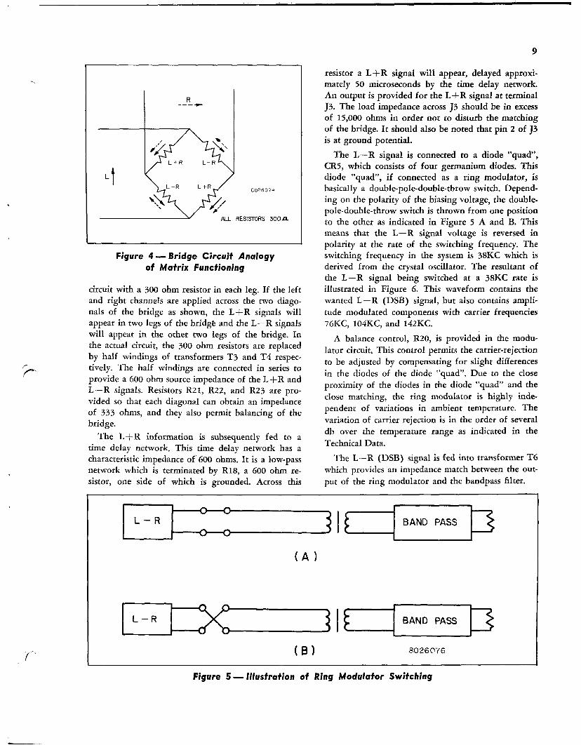
The functioning of the matrix can be visualized in Figure 4. Illustrated in Figure 4 is a common bridge
I ‘f’
L
BTS- IA STEREO
SUBCARRIER GENERATOR
COMPOSITE SIGNAL
L+R L-R (DSB) PI LOT
BTE - 108 EXCITER
MI - 560004 ADAPTER TRANSMITTER
8026073
Figure 2 - Simplified Diagram Showing Relafionship of BTS-7A to Exciter and Transmitfer

POWER
t
SUPPLY I 17, 208, 240,k II VAC, 50/60 CPS)
+ IO5 V(30MA) 6.3 VAC( IA)
OSCILLATOR
MATR ‘IX
: I I I
t
38 KC
I PHASE AMPL. PILOT
23-53KC L-R (DS9)
L-R RING BANDPASS
MODULATOR FILTER P=
AMPL.
TIME LfR
w * DELAY NETWORK
L+R
BRIDGING OUTPUT
19KC
RELAY
ToNo
I
I I --- J
L+R
L- R (DS81
PILOT
8026075
m
R ---+
Figure 4 - Bridge Circuit Analogy of Matrix Funcfioning
circuit with a 300 ohm resistor in each leg. If the left and right channels are applied across the two diago- nals of the bridge as shown, the L+R signals will appear in two legs of the bridge and the L-R signals will appear in the other two legs of the bridge. In the actual circuit, the 300 ohm resistors are replaced by half windings of transformers T3 and T4 respec- tively. The half windings are connected in series to provide a 600 ohm source impedance of the L+R and L-R signals. Resistors R21, R22, and R23 are pro- vided so that each diagonal can obtain an impedance of 333 ohms, and they also permit balancing of the bridge.
The L+R information is subsequently fed to a time delay network. This time delay network has a characteristic impedance of’600 ohms. It is a low-pass network which is terminated by R18, a 600 ohm re- sistor, one side of which is grounded. Across this
9
resistor a L+R signal will appear, delayed approxi- mately 50 microseconds by the time delay network. An output is provided for the L+R signal at terminal J3. The load impedance across 53 should be in excess of 15,000 ohms in order not to disturb the matching of the bridge. It should also be noted that pin 2 of 53 is at ground potential.
The L-R signal is connected to a diode “quad”, CR5, which consists of four germanium diodes. This diode “quad”, if connected as a ring modulator, is basically a double-pole-double-throw switch. Depend- ing on the polarity of the biasing voltage, the double- pole-double-throw switch is thrown from one position to the other as indicated in Figure 5 A and B. This means that the L-R signal voltage is reversed in polarity at the rate of the switching frequency. The switching frequency in the system is 38KC which is derived from the crystal oscillator. The resultant of the L-R signal being switched at a 38KC rate is illustrated in Figure 6. This waveform contains the
wanted L-R (DSB) signal, but also contains ampli-
tude modulated components with carrier frequencies 76KC, 104KC, and 142KC.
A balance control, R20, is provided in the modu-
lator circuit, This control permits the carrier-rejection
to be adjusted by compensating for slight differences
in the diodes of the diode “quad”. Due to the close proximity of the diodes in the diode “quad” and the
close matching, the ring modulator is highly inde- pendent of variations in ambient temperature. The
variation of carrier rejection is in the order of several
db over the temperature range as indicated in the
Technical Data.
The L-R (DSB) signal is fed into transformer T6
which provides an impedance match between the out-
put of the ring modulator and the bandpass filter.
L-R 0 c
(A)
(6) 8026076
Figure 5- Illustration of Ring Modulafor Swifching

- --- ,
10
Figure 6 - The Combining of L - R Signal
and 38 KC Carrier
Matrix Znputs md Outputs
The main reason for matrixing is compatibility.
Thus a person who is not equipped to receive stereo
will be able to receive the same information mono-
phonically.
Refer to Figure 7, during this brief explanation
on how the matrix functions: The different sketches
illustrate the outputs of the matrix for different types
of inputs.
In Figure 7A, if both left and right channels are
fed with a sine wave in phase, there will only be an
output from the LfR channel with twice the magni-
tude of the input signal. There will be no output at
the L-R channel.
In Figure 7B, a sine wave is fed into the left (L)
channel. The outputs are sine waves which equal one-
half of the input but still in phase with the input
sine wave,
In Figure i’C, a sine wave is fed into the right (R) channel. The output here is also one-half the input magnitude, however the L+R signal is in phase with the input but the L-R signal is of opposite polarity.
In Figure 7D, shows input signals to the left and right inputs with the same frequency, same amplitude but opposite polarity. This provides an output signal from the L-R channel which is in phase with the
input to the left (L) channel. There will be no output
from the L+R channel.
Figure 7E and 7F illustrate two other examples of
what the outputs of the matrix would be for given
inputs.
Filter Network
The bandpass filter has a 3 db bandwidth of 36KC
with a center frequency of 38KC. This filter will
eliminate all components outside a range from 23 to
53KC. It is particularly effective in removing compo-
nents in the band of frequencies utilized by SCA
subcarriers.
Any spurious components in a frequency range from 57KC and above, will be attenuated better than -70 db relative to 100% modulation on the main carrier. This means -50 db relative to an SCA subcarrier with a modulation percentage of only 10%. (See Figure 8.)
The bandpass filter is terminated with resistors Rli’ and R16 which total 3600 ohms. At this location, an L-R (DSB) signal is present. This signal is con- nected’ in series, that is, added to the L+R signal which appears across R18; and in order to match the amplitude of both signals properly, the L-R (DSB) signal is adjustable with R16.
Composite Signal
The composite signal also has a 19KC pilot signal
along with the L+R and L-R (DSB) signals. This
19KC pilot appears across resistor R15 which is also
connected in series with R18 and R16. Thus, at this
point the three signals (L+R, L-R (DSB) and
loKC) are added together forming the composite
signal which appears at output terminal 54. The com-
posite signal can also be measured from the front
panel at test point J9.
The availability of the composite signal at the out-
put has several advantages. It is easy to adjust modula-
tion percentage and pilot phasing. Waveforms for
this purpose can be observed on the oscilloscope with-
out the need of FM detection. Figure 9 shows a wave-
form obtained with proper phasing of the 19KC pilot.
To obtain this waveform, equal signals out of phase
are fed into the left and right inputs of the matrix.
The top waveform in Figure 9A represents a modu-
lating frequency which is not an integral sub-multiple
of the carrier frequency, while the bottom waveform
of Figure 9B shows a modulating frequency being an
exact sub-multiple of the carrier frequency. Figure 10A
shows incorrect phasing with a pilot carrier being
approximately 45O out of phase, and Figure 10B
shows correct phasing with a left or right signal only.

. -
+-- L L+R b+-
cl
MATRIX
R L-R *+
L i-R
L -R
2L
A. 8.
L L+R *+
cl
MATRIX
-4T R L-R ,+
L+R
-(L-R)
C.
E. F.
8026077
Figure 7 -Examples of Matrix Outputs for Different Type Inputs

‘-
Odb 1 -lOO‘!& = t75 KC
-lO-
-20 -
-3o-
-4o-
-5o-
-6O-
-7o- /////////////I//////
SPURIOUS -80- COMPONENTS
- so-
l L-
i
3OCPS 15000cPs
19KC PILOT
I 30
SPURIOUS COMPONENTS
(EXCEPT ~RD ORDER
DISTORTION)
38 KC SUB CARRIER
SPURIOUS COMPONENTS FROM MAIN AND DSB SIGNALS
I I I I I I * 60 70 80 so KC
67 KC SCA SUBCARRIER 8026078
BTS-I A SPECTRUM DISTRIBUTION *
..-..-. J.

Figure 9 -Proper Phasing of 79 KC
Pilot Signal Figure 10 -Effecfs on Composite Signal
Due fo Pilot Phasing
Stereo Mono Relay
Part of the series connection of R18, RIG, and Rl5 can be short circuited using relay Kl. This relay can be actuated locally or remotely; locally by closing switch S2, and remotely by closing contacts 15 and 16 of J5.
For stereo operation, relay Kl will be energized and the contacts which short R15 and RIG, will open. The other contact will close and apply power to pilot light DS2 indicating that the subcarrier generator is
in the stereo mode.
Crystal Oscillator
The crystal oscillator which operates at 38KC can
be varied 2 cps by capacitor C2, however the oscil-
lator does not normally require any adjustment. This
38KC signal can be checked at J6.
The 38KC signal is amplified in the triode section
of Vl and then fed to the ring modulator. The switch-
ing frequency of 38KC does not contain any compo-
nents at 19KC or 57KC. Both components are very
difficult to remove from the composite signal since
they are very close to the edges of the bandpass filter.
The 38KC signal from the oscillator is also fed to a regenerative divider (V2) where the 19KC pilot signal is obtained. The divider is very stable, maintaining lock-in for synchronizing voltage variations of 40 db and plate voltage variations in excess of 50%. The output of the divider can be checked at J7. The ampli- tude of the 19KC pilot frequency can be varied using Rl5 while the phase of the pilot can be adjusted by
means of L2. With the amplitude adjustment Rl5 full CCW, the amplitude of the pilot appearing in the composite signal is attenuated at least 60 db. This will facilitate the precise adjustment of the rejected 38KC carrier signal.
It is imperative that correct phase is maintained since all demodulating systems display a certain amount of sensitivity to phase errors. Most sensitive to phase errors are the time switching and AM syn- chronous detection systems, while the AM envelope detection method has a lesser dependency on pilot phase. Should the pilot phase error be +-90 degrees, a left to right channel reversal will take place. The amplitude of the pilot can be adjusted to give modu-
lation percentages between 0 and 15% on the main channel.
Power Supply
The power supply of the BTS-1A utilizes silicon rectifiers to provide 105 volts dc for tubes Vl and V2.
A break-down diode (CR6) is provided to maintain the plate voltage at 105 volts. This voltage can be checked at test point J8. The power transformer T8, also provides 6.3 volts ac to operate relay Kl and the filaments of Vl and V2. The sub-carrier generator can be operated from any line voltage between 106 to 128 volts ac, and 197 to 251 volts ac at 50 or 60 cycles.
Input Adapter
An Input Adapter MI-560004, is used to replace the input transformer, TlOl, in the BTE-1OB Exciter. Re- fer to the schematic diagram Figure 25. The replace- ment of TlOl is necessary to extend the frequency

- --- -- ___..- ,
14
response to a range from 5 cycles to approximately 8OKC. This wide frequency response is required to accommodate the composite stereo signal without de- terioration of left versus right channel separation. The input adapter contains one tube V401.
The adapter is powered from the BTE-1OB Exciter. Voltages of 6.3 dc and 150 dc are provided for the filament and plate respectively. One section of the dual triode (type 6922) is used as a wideband phase splitter, providing equal and opposite phase voltages to be fed to the grids of the reactance tubes in the exciter.
the BTX-1A is used simultaneously with the BTS-1A
for simultaneous stereo and SCA transmissions. The
purpose of this filter is to remove any components
(at the BTX-1A output) below 53KC to a level of
-60 db or better relative to 100% main carrier modu-
lation. This is to prevent interference from the SCA
channel into the stereo subchannel.
The other section of V401 is used to overcome load- ing of the automatic frequency control loop by a 270K resistor (R410) and .33 mf capacitor (C405). The input adapter is mounted where TlOl would normally be located.
Band Pass Filter
A Bandpass Filter (MI-560003) is provided to be installed in the BTX-1A subcarrier generator in case
Two connections are necessary to connect the filter
into the BTX-IA. The filter is a bandpass with a total
bandwidth of 17KC and a center frequency of 67KC.
The use of the bandpass filter, which has become
necessary due to the introduction of the stereo sub-
channel, will cause a slight increase in harmonic dis-
tortion of the SCA channel. This increase will be more
pronounced at higher modulating frequencies than at
lower modulating frequencies. At 400 cycles, harmonic
distortion at the SCA subcarrier generator will be in
the order of 2%.
INSTALLATION
-
Carefully unpack and inspect the equipment to
make certain that no damage has been incurred during
shipment. Any damages or shortages should be im-
mediately reported to RCA and to the transportation
company in order that lost or damaged material may
be recovered.
The BTS-IA is shipped complete in one container;
but, MI-560003 and MI-560004 are packed in separate
boxes. All internal wiring is hone at the factory; only
external cables and wiring need be prepared and con-
nected to the equipment during installation.
BTE-1 OB Conversion
Disconnect all leads from terminals of TlOl (input
transformer) and remove transformer from chassis;
save the mounting hardware. Discard transformer
and the following components; R108, R109, RllO,
Rlll, Terminal E20 (next to terminal 9 of TlOl)
and wires between terminals 6 and 15 of TlOl, 4 and
6 of X2101, and the wires between terminals E20
and E19.
Install small Input Adapter chassis (MI-560004) in place of TlOl; insert input adapter from rear of chassis and mount using TlOl mounting hardware. Orient such that electrolytic capacitor is right over the tube. Connect leads as shown in Figure 25. Utilize shielded cable to connect adapter to shock-mounted
subchassis. Make sure that the lead from Pin 1 and 6 of V401 goes to the grid of V102 of the exciter, and the lead from pin 3 of V401 goes to the grid of VlOl of the exciter. Check the operation of the automatic frequency control system. A small amount of retuning will be required at the rear adjustment of TlO3. Set Cl05 for maximum deflection of Ml01 with switch in the VlOl + V102 I, position, or set for maximum deviation as indicated on a modulation monitor. Figure 23 shows a completed conversion.
BTS-1 A Stereo Subcarrier Generator
Remove the pre-emphasis network ZlOl from the exciter and insert in the BTS-1A Stereo Subcarrier Generator. Also insert second pre-emphasis network as well as C13, filter capacitor, packed with the BTS- 1A (Items 2 and 3 of MI-560001).
Connect taps of transformer T8 in accordance with
the proper line voltage. Refer to Table 1.
The equipment is shipped with the taps set for
240 V operation.
The unit can be operated at power line frequencies
of 50 to 60 cps. No change is required.
The circuit breaker Sl can at the same time be used as POWER ON-OFF switch if desired.
Using the enclosed power line plug (Item 4 (C) of MI-560001) connect the BTS-1A to suitable point in

- . -
/
15
TABLE 1 - TRANSFORMER PRIMARY TAPS
Power Line Voltage 106 117 128 197 208 219 229 240 251
Taps to be Used 3-4 2-4 1-4 3-5 2-5 1-5 3-6 2-6 1-6
the associated equipment. (e.g. Terminals lE2 and lE3 in the driver rack of the BTF-5/10 FM trans- mitters. By connecting to these terminals, the BTS-1A Stereo Subcarrier Generator is automatically provided
with line voltage whenever the transmitter is switched on.)
i)
Connect audio lines to Left (L) and Right (R) channel inputs (Jl and J2) using plugs Pl and P2 which are provided as Item 4 (A) of MI-560001. Be
sure to maintain proper polarity in the L and R channels.
For monophonic operation equal signals should be fed to L and R inputs. If only one line is used, the input to either left or right inputs must be increased by 6 db.
Provide interconnecting cable from 54 of the BTS- 1A to 3401 of the MI-560004 input adapter, using plugs provided as Item 4 (B) of MI-560001 and Item 2 of MI-560004. Use RG58A/U cable or equiva- lent. Make this cable as short as practical, preferably not longer than 15 feet.
A bridging output is provided at J3. Note that the load impedance should not be less than 15,000 ohms. Terminal 2 of 53 (the small slot) is connected to ground. At this output a LfR signal is present. Check that the tubes, relay, pre-emphasis network, capacitor, crystal and the ring modulator, CR5, are properly seated in their respective sockets. Power can now be applied by clqsing Sl. The green pilost light DSl will light when power is applied to the unit and Sl is in the ON position. Place S2 in the STEREO ON position.
Initial Adjustments
The following adjustments are made in the factory before the unit is shipped; however, they may be re- peated to confirm proper operation of the complete system.
1. Adjust R20 (Balance) for minimum voltage at J9 test point with RI6 fully CW and Rl5 fully CCW.
2. Voltage at J9 should be 7mv,,, or less (use HP330 distortion analyzer, meter position set for
3°mvRMs full scale).
NOTE: For the following steps, set oscilloscope for approximately 500 &cm sweep rate when using the J9 test point. Use 400 cps signal to synchronize the oscilloscope.
3. With L only input to Jl at 400 cps and +10 dbm, adjust Rl6 for proper balance L+R vs. L-R (DSB). Use scope on J9 test point. Display to re- semble Figure 11 or 1SE.
4. With 400 cps at +lO dbm 180’ out of phase to
Jl and J2, adjust L2 “Pilot Phase” to resemble
Figure 9.
5. Adjust Rl5 for’ 8 to 10% pilot modulation as
indicated on station monitor (25 to 35mv,,, at test
point J9). ,
Remote Switching
Switching from stereo to mono modes and vice
versa is accomplished by switch S2 and relay Kl.
Whenever the unit is in the stereo mode an indicator
light marked “Stereo” will be lit.
Switch S2 will override any remote commands.
Open S2 for remote control. To control the mode
from a rem&e point, connect two lines to terminals
15 and 16 of J5. Provide SPST switch at the remote
end of this line. Closing this switch will put the BTS-
1A in the stereo mode.
Should remote control over telephone lines be desired a latching relay panel MI-27509A must be installed at the BTS-IA location. Connect terminals 15 and 16 of J5 of the BTS-1A to terminals 3 and 7 of the MI-27509A Latching Relay Panel. Connect leads 4 and 8 to one side of a 117 V AC supply. The other side of the 117 V AC supply should go to proper terminals (depending on position used) in the A and C banks of terminals on the BTR-11A or 20A transmitter control units (MI-27526 or 27538). Ter- minal 5 of the latching relay panel should be con- nected to a terminal in the B bank and terminal 9 should go to the D bank, Further information is contained in the instruction book for the BTR-1lA and BTR-20A Remote Control Systems.
Simultaneous Use of Stereo and SCA Subchannels
If simultaneous use of stereo and SCA subchannels is desired, an MI-560003 filter must be installed in the BTX-IA Subcarrier Generator to attenuate com- ponents of the 67 kc subcarrier. Information for proper installation is given in Figure 24.
This will complete the installation.

16
TUNE-UP PROCEDURE
The BTS-1A Stereo Subcarrier Generator is properly tuned before shipment. No further adjustments are normally required to put it into operation. However, if there is any indication of improper operation, the following steps may be taken:
1. With the unit operating, connect a frequency counter to test point J6. A frequency of 38KC t2 cps should be read. With the frequency counter con- nected to test point 57 a frequency of 19KC 21 cps should be read. At room temperature both readings will be within a fraction of one cycle of the proper frequencies. A small adjustment of the oscillator fre-
quency is possible through adjustment of C2.
2. To check proper operation of the divider, test points J6 and J7 should be used to obtain a Lissajou pattern. Further details are given under Maintenance.
3. Apply a + 10 dbm signal at 400 cps to Jl; close S2; connect an oscilloscope to test point J9; set vertical gain for full deflection with approximately 700 mv peak-to-peak; connect 400 cps modulating signal to EXT. SYNC. of oscilloscope and adjust sweep rate to display about 2 cycles of the 400 cps waveform. Turn Rl5 full CCW. An oscilloscope dis- play similar to Figure 11B should be obtained. Adjust Rl6 for straight base line. Figure llA, taken with modulating signal being an exact sub-multiple of the 38KC carrier, and 1lB shows a random L or R signal
Figure 77 - Waveform Showing Proper Ratio of L + R and L - R fDSBl Signals
If the display is similar to Figure 12A, turn Rl6
CM; if it is similar to Figure 12B turn RIG CCW.
Figure 12A indicates amplitude of L-R (DSB) is
too low, and Figure 12B indicates the same is too
high. Figures 13A and B represent a condition of
excessive time delay error which will result for modu-
lating frequencies of approximately 16 to 17KC. To
obtain the display shown in Figure 14A and B, equal
out-of-phase signals must be applied to Jl and J2.
NOTE: Displays in Figures 1lA and 14A are obtained with modulating frequencies which are exact sub-multiples of the 38 kc carrier, while the display in Figures IIB and 14B represent a random condition between both frequencies.
The waveforms shown in Figure 15A and B repre-
sent conditions of severe over-modulation. They are
obtained with signals at Jl or J2 or both, in the order
of t-20 dbm.
4. To check proper balance of suppressed carrier,
turn R15 full CCW; leave setting of Rl6 as deter-
mined in step 3; remove all signals from Jl and J2.
Measure voltage at J9 with VTVM having a response
at least up to SOKC. Adjust R20 to bring this voltage
to a minimum, but at least to Tmv,,,. (An oscillo,
scope may be used instead of the VTVM; use internal
synchronization; check for less than 20 mV p-p.)
Figure 12 - Waveforms Showing Amplitude of
L - R iDSBI Too Low and Too High

-, -
16
TUNE-UP PROCEDURE
The BTS-IA Stereo Subcarrier Generator is properly tuned before shipment. No further adjustments are normally required to put it into operation. However, if there is any indication of improper operation, the following steps may be taken:
1. With the unit operating, connect a frequency counter to test point J6. A frequency of 38KC +2 cps should be read. With the frequency counter con- nected to test point 57 a frequency of 19KC r+l cps should be read. At room temperature both readings will be within a fraction of one cycle of the proper frequencies. A small adjustment of the oscillator fre- quency is possible through adjustment of C2.
2. To check proper operation of the divider, test points J6 and J7 should be used to obtain a Lissajou pattern. Further details are given under Maintenance.
3. Apply a + 10 dbm signal at 400 cps to Jl; close S2; connect an oscilloscope to test point J9 ; set vertical gain for full deflection with approximately 700 mv peak-to-peak; connect 400 cps modulating signal to EXT. SYNC. of oscilloscope and adjust sweep rate to display about 2 cycles of the 400 cps waveform. Turn R15 full CCW. An oscilloscope dis- play similar to Figure 1lB should be obtained. Adjust R16 for straight base line. Figure llA, taken with modulating signal being an exact sub-multiple of the 38KC carrier, and 1lB shows a random L or R signal
Figure 11 - Waveform Showing Proper Rafio of L + R and L - R lDSBl Signals
If the display is similar to Figure 12A, turn Rl6
CW; if it is similar to Figure 12B turn R16 CCW.
Figure 12A indicates amplitude of L-R (DSB) is
too low, and Figure 12B indicates the same is too
high. Figures 13A and B represent a condition of
excessive time delay error which will result for modu-
lating frequencies of approximately 16 to 17KC. TO
obtain the display shown in Figure 14A and B, equal
out-of-phase signals must be applied to Jl and J2.
NOTE: Displays in Figures 11A and 14A are obtained with modulating frequencies which are exact sub-multiples of the 38 kc carrier, while the display in Figures 11B and 14B represent a random
condition between both frequencies.
The waveforms shown in Figure 15A and B repre-
sent conditions of severe over-modulation. They are
obtained with signals at Jl or J2 or both, in the order
of +20 dbm.
4. To check proper balance of suppressed carrier,
turn Rl5 full CCW; leave setting of Rl6 as deter-
mined in step 3; remove all signals from Jl and J2.
Measure voltage at J9 with VTVM having a response
at least up to 50KC. Adjust R20 to bring this voltage
to a minimum, but at least to Tmv,,,. (An oscill.o-
scope may be used instead of the VTVM; use internal
synchronization; check for less than 20 mV p-p.)

/1
h ,--
Figure 13 -Effects of Excessive Time Delay
5. To adjust the pilot amplitude turn R15 CW
until an indication between 8 and 10% is obtained
on a modulation monitor.
To adjust the pilot phase, apply equal out-of-phase
signals (at 400 cps) to Jl and J2. Adjust L2 to re-
semble waveform of Figure 9A.
Figure 1OB shows proper phase with an L or R
only signal. (So does Figure 18B.)
Figure 1OA shows a signal with approximately 45O
phase error. If an L only signal is fed to the unit, the
pilot lags 45O; with an R only signal, the pilot leads
45O.
To check phasing in conjunction with a stereo
adapter, connect the output of the BTS-1A Stereo
Subcarrier Generator to the input of the adapter.
Apply 400 cps equal amplitude, opposite phase
signals to Jl and J2. Proper pilot phasing (by adjust- ing L2) should coincide with maximum signal from
the L and the R channel output connectors of the
Stereo adapter.
When a signal is applied to Jl only, the adapter
should provide a signal in the left (frequently desig-
nated A channel) output.
With an oscilloscope display as shown in Figure 18B, adjust the separation control in the Stereo adapter for maximum unwanted channel rejection. (At 400 cps a ratio of 40 db of the wanted to the unwanted channel can be obtained with a good adapter.)
The adapter should then be connected to a regular PM receiver (designed for stereo operation). Any
Figure 74 - Resuh When Equal and Out of Phase Signals are Applied fo .I7 and I2
Figure 15 - Effecfs of Severe Overmodulation
deterioration of separation (due to slight variations
in the frequency response of the exciter and receiver)
can be compensated by advancing Rl6 in a CW
direction.
NOTE: Many older FM tuners, especially ones using discriminator type detectors are sensitive to resistive and capacitive loading thus unduly reduc- ing the L-R (DSB) signal amplitude. This will affect L vs. R channel separation. Any such dis- crepancy should not be corrected by advancing Rl6 in the BTS-1A since it will reduce separation in
properly operating equipment.

- -
18
MAINTENANCE
All components in the BTS-1A Stereo Subcarrier Generator are selected to give long, maintenance-free service. The tubes carry a 10,000 hour guarantee; however, they should be checked after the unit has been in operation from 1 to 2 years.
The relay contacts should be cleaned with a proper spatula if noises during mono-stereo switchover indi- cate dirty contacts.
If capacitor Cl3 fails, a replacement unit can be plugged in immediately. If such a replacement unit is not available, any single capacitor of .5 mf or more and a voltage rating of at least 100 V DC connected to pins 5 and 1 (5 being positive relative to 1) will provide sufficient plate voltage to keep the BTS-1A in operation.
Failure of the relay I<1 can temporarily be corrected by removing the relay from its socket. The unit will then be in the stereo mode. In the monophonic mode the pilot will not be removed.
If tube Vl fails, any of the following tubes can be used if the 7643 should not be available: 6U8, 6U8A, 7731, 6BL8, E80CF, or ECFSO.
If tube V2 fails, any of the following tubes can be used if the 6922 should not be available: 6DJ8, 7308, 6FW8, E88CC, or ECC88.
The green pilot light uses a standard #47 bulb. It is operated below its rated voltage and should have a life in excess of 10,000 hours.
Matrix Balancing
Should it be desired to check the initial balance of the matrix the following steps should be taken:
Remove CR5 from its socket. Connect a 600 ohm resistor from pin 2 to 6. Remove Zl and Z2 and apply jumpers between pins 3 and 4 and between pins 5 and 6 of XZl and XZ2.
Connect an audio generator to Jl ar,d J2 in such a way that the two signals are in phase. (Pin 1 of Jl to pin 1 of J2, and pin 2 of Jl to pin 2 of J2.) Adjust audio input level to approximately + 10 dbm at 12KC.
Connect an AC VTVM (e.g. Distortion Analyzer) to 53 (use pin 1 of 53 which is the wide terminal and ground) and note reading, or set to 0 db. Then con- nect AC VTVM to pins ? and 6 of XCRS. With a 12 kc input signal being fed in, set R23 for minimum voltage. This voltage should be attenuated at least 50 db relative to the voltage in the L+R channel. For any frequency below 10 kc, L-R rejection should be better than -60 db. After balancing is completed, reinsert Zl, 22, and CR5.
DC Voltage Readings
Table 2 shows DC voltage readings at the tube pins;
the plate voltage, measured at test point JS should be
flO5 v f5%.
AC Voltage Readings
All voltages connected with the crystal oscillator
will vary slightly depending on the setting of C2.
Table 3 s’hows AC voltage readings at the tube pins.
Additional voltages can be measured at points given
in Table 4.
The waveforms shown in Figure 17 will provide
additional information.
The small spikes seen in Figure 17E are stationar)
when the divider is properly locked in. The range of variation of ~2 is too small to affect lock-in of the
divider. Transformer T7 contains an adjusting pin (left handed thread) which will permit it to vary the
inductance of its windings. This pin is adjusted before shipment to give o” phase of the 19 kc pilot with L2
set to its mid-position.
TABLE 2- BTS-IA TUBE VOLTAGES (DC)
CONDITIONS: All measurements (taken with RCA Senior Voltobmyst) made under normal operating conditions.
All readings DC and taken relative to ground. Allow 3110% tolerance.
Pin Numbers Symbol We
1 2 3 4 5 6 7 8 9
V1 7643 80 -1.8 65 - - 95 - 2.3 0
v2 6922 85 0 7.8 55 -.2 7.8 - - -
v401* 6922 90 16 17.5 - 6.3 90 16 17.2 -
* Located in Input Adapter MI-560004.

TABLE 3 -BTS-IA TUBE VOLTAGES (AC)
Q 50 or 60 cps, depending on power line frequency.
** 38 KC
TKC
NOTES : (I) Vpp = volts peak-to-peak.
(2) Read oscillator plate circuit voltage at junction of Ll and R2; voltage should be 30 Vpp at 38 KC.
(3) Read divider grid voltage at junction of T7 and Rl3, voltage should be 35 Vpp at 19 KC.
(4) Waveform appearing at pin 2, XV2 is not sinusoidal. Some vacuum tube voltmeters may cause erroneous readings. If in doubt, use oscilloscope. (See Figure 17F.)
Variation of L2 will also slightly change the ampli-
tude at testpoint J7.
The captions of Figure 18A to F, and Figure 19A
and B, will fully explain the conditions under which
the waveforms were obtained.
Input Adapter
Components in this unit are selected to give long,
maintenance-free service. The tube carries a 10,000
hour guarantee. It should be checked after I to 2 years
of service.
Voltage values are listed in Table I.
To check for proper AC operation, apply 400 cps
at .5 vI~~fs to J401. Check AC voltages appearing at
pins 3 and 6 of XV401. Both voltages should be alike
and somewhat less than .jRlfS.
It is the purpose of one triode section of V401 (pins 6, 7, 8) to provide feedback for proper phase-
amplitude correction in the AFC loop. If this tube
fails, the center frequency wil! pulsate at a slow (1
cps) rate around the center frequency. This tube repre- sents a variable load between pins 1 and 3 of the
other triode section (pins 1, 2, and 3).
Any slow-varying voltage appearing across Cl04 in the exciter will likewise appear at pin 3 of V401 and in opposite phase at pin 1 of V401. In this manner, excessive phase shift on the AFC voltage caused by R410 and C405 is compensated.
The tube type 6922 can be replaced by the same
equivalent types as listed under V2 of the BTS-IA if
the exact replacement should not be immediately
available.
With the adapter installed, and the selector switch
of the exciter in the + or - AFC position, the
pointer of Ml01 (on exciter) will display a slightly
higher degree of random variation. This is a normal
condition and does not affect the proper operation.
Measurement of 1 vs. R Channel Separation
The waveform in Figure 16 illustrates separation
between left and right channels. The actual waveform
can be observed at testpoint J9 of, the BTS-IA or at
the multiplex output of an FM-tuner. It shows a
composite signal without pilot, but with a L only or
R only input to the BTS-IA sterio subcarrier gen-
erator. The ratio of the amplitudes A and B will deter-
mine separation. Use formula given to obtain the
ratio in db (Separation = Log A/B). For a perfect
signal, the B amplitude would be zero, (by proper
setting of R16) separation therefore infinite and the
baseline perfectly straight. The above method will
become inaccurate for separation ratios in excess of
approximately 36 db due to the inability to read the
small amplitude correctly. Some slight improvement
can be gained by displaying the upper or lower half-
wave only.

SEPARATION = 20 LOG f$
8026079
Figure 16 - Illusfrafion of Basic Mefhod to Measure Separafion
TABLE 4 -VOLTAGES AT VARIOUS LOCATIONS FOR GIVEN FREQUENCIES
Junction Voltage
Yl - C2 to GND 4 v P-P C2 - C4 to GND 10 v p-p
Test Points Voltage
Frequemy
at 38 kc
at 38 kc
Frepency
J6 to GND
J7 to GND
30 v p-p
2 v P-P
at 38 kc
at 19 kc
J9 See Oscilloscope Displays, Figures 17 to 19
Across Terminals
4-5 of T5
7-8 of T8
9- 10 of T8
3-4 of T7
Voltage Frequency
2 v P-P at 38 kc
100 V rms at 50 or 60 cps
6.3 V rms at 50 or 60 cps
approx. 40 mv rms at 19 kc

.- 7
21
NOTES:
1. Waveforms taken with Tektronix Type 585 scope. Hewlett Packard Type 130-B or 150-A may be used.
2. Waveforms of Figure 17 A to F and waveforms A and C of Figure 18, were taken with internal sync, all others are of external sync by modulating waveform.
3. Squares on graticule equal 1 centimeter (horizontally and vertically); psec/cm refers to sweep time base, and V/cm refers to vertical calibration.
A. Vl Pin 2 B. Vl Pin 1
10 usec/cm. Iv/cm 10 usec/cm, 5v/cm
C. Vl Pin 8 D. 15 Terminals 4 and 5
10 usec/cm. .5v/cm 10 usec/cm, .Iv/cm
I
?
E. V2 Pin 2 F. V2 Pins 3 and 8
10 usec/cm. Iv/cm 10 usec/cm, Iv/cm
Figure 17 - 6% I A Reference Waveforms

22
A. T6: Btwn. terminal 6 and gnd.
+lj db input to Jl at 400 cpa
.5 millisec/cm, .5v/cm
C. J7
10 use-z/cm, .5v/cm
B. J9; +13 db input to Jl
at 400 cps. pilot included
.5 millisec/cm, .5v/cm
D. J7 to Vert. and J6 to Horir. Ampls.
equal deflections
E. J9: +13 db at 400 cps to Jl
R15 full ccw, correct balance .5 millisec/cm, .5v/cm
F. J9; insufficient L-R (DSB) Ampl.
R15 full ccw
.5 millisec/cm, .5v/cm
Figure 18 - BTS- 1 A Reference Waveforms
A. J9; Time delay error only
(-5 db at 16 KC to J11
R15 full ccw
20 usec/cm, .5v/cm
8. J9; lime delay and amplitude error
R15 full ccw
20 usec/cm, .bv/cm
Figure 79 - BTS-IA Reference Waveforms

i
22 SI
Figure 20 - BTS-IA Stereo Subcarrier Generator, Front View
24
!Q a
I \
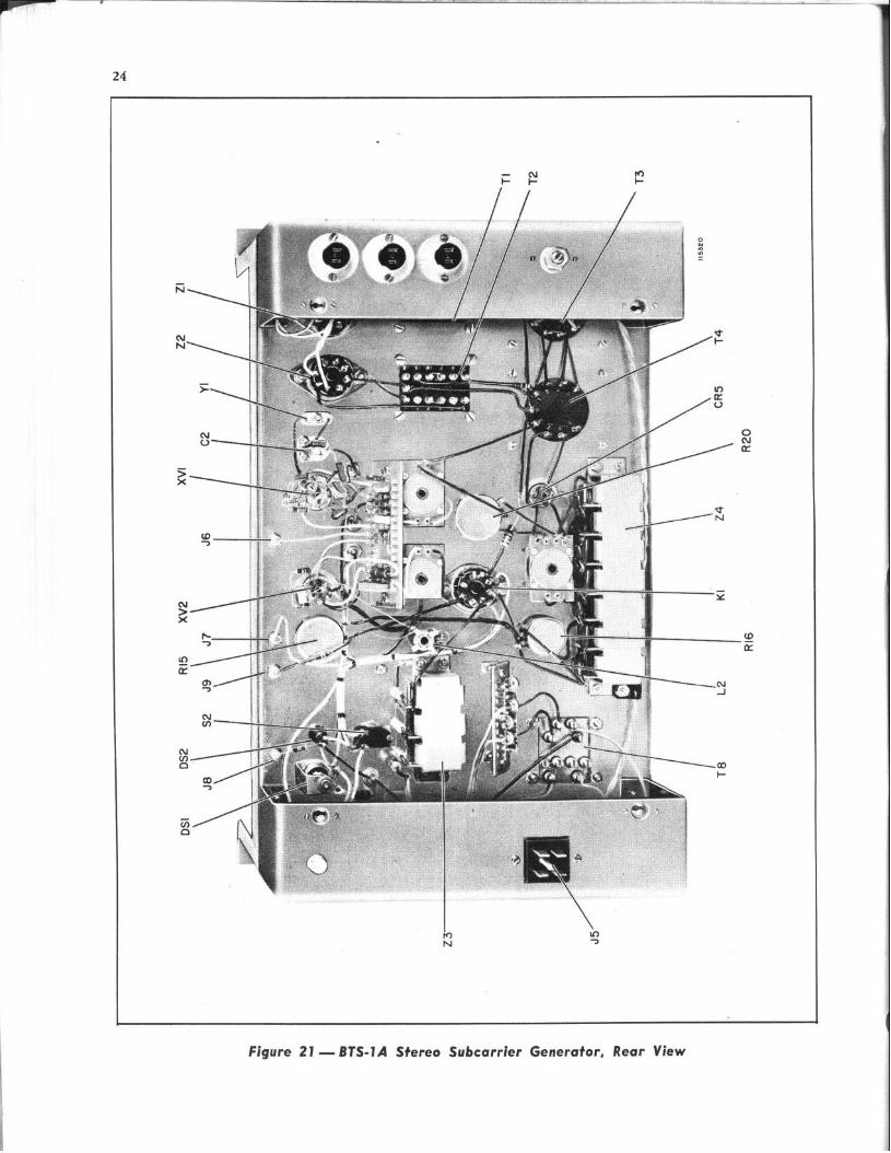
Figure 21- BTS-IA Stereo Subcarrier Generator, Rear View

Figure 22 - BTS-IA Stereo Subcarrier Generator, Rear View
.

26
TERMINAL BOARD
I I I I I I I I I I I I
$0 4Lo2 4cos 4L0, 49 4:s 4% 4!7 4:s 4i2 64 4Ro3
I I I I I I I I ,I I I I . I
TO SIOI
/ c40
’ ’ AVIOl \
115318
Cl29 Cl20 c403
7 c405 c404 xv401 TO VI02
Figure 23 - Input Adapfer Ml-560004, Componenf Idenfificafion; Shown Installed in BTE-IOB Excifer

Symbol Stock No. Drawing No. Description
STEREO SUBCARRIER GENERATOR, MI-560001
CAPACITORS
c”:
2
cc:
33 c9 Cl0 Cl1 Cl2 C13A/B CR1 CR2 CR3 CR4 CR5 CR6 DSl DS2 Jl J2 J3
s! J6
3 J9 Kl
LL:
;:
;: p5
057602
215276
gg3oz6-zzg 8886256-7
993026-465 993026-457 993026-453 737863-17s
098402
990786-213 737863-175 990786-213 737863-183 993x6-673 ggjoz6-ztg
225279 225200
735712-53
MICA, 47 PF 510% 500 V VARIABLE. 4.5-25 PF MICA, 1560 Pi t$% 500 V !lICA, 680 PF 15% 500 V MICA; 470 PF i5% $00 V PAPER, 0.1 MF *20% 200 V FILM, 10 NF i2OX 200 V SAME AS c6 SAtiE AS C7 PAPER. 0.47 MF 220% 200 V MlCA;3.3 NF rt2% 500 V MICA, 18 PF rtlO% 500 V ELECTROLYTIC, 60/60 MF 150 V DIODE - SILICON SAME AS CR1 SAME AS CR1 SAME AS CR1
225202 225201
225203 211510
miw 208983
203532
094864
EZ44 211509
ggO158-12 8524111-l
%1:;;-; 481&z
’ 38W 15’ 8825493-7 8825493-7 8825493-2 8825493-T 8971187-3 8528117-1
DIODE - QUAD DIODE - ZENER LAMP - INDICATOR, TYPE 47 SOCKET - PILOT LIGHT, WITH LAMP AND AMBER JEWEL CONNECTOR - FEMALE, 2 CONTACT SAME AS Jl SAME AS Jl CONNECT R
8 -
CONNECT R - i%WE4 8fiVAtt CONNECTOR - TIP jACK, YELLOW SAME AS J6 CONNECTOR - TIP JACK, RED SAME AS J6 RELAY - 6 V AC, D.P.D.T. CONTACTS CHOKE - 47 MlLilHENRY COIL - ADJUSTABLE. 1000-2000 MICROHENRY
92135 3
1510013-101 05210 727969-14
CONNECTOR - MALE,'2 CONTACT SAME AS Pl SAME AS Pl CONNECTOR - MALE, COAXIAL CONNECTOR - FEMALE, 4 CONTACT
RI
;; R4 R5 R6
3 R3 RlO Rll R12 RI3 R14 Rl
2 i17 R18 R19
Is? R22 R23
82283-08 2
.IESISTORS FIXED COMPQSITION - UNLESS OTHERWISE SPECI
82283-83 82283-72
g&g g;;;:; 1: 82283-78 82283-62 ?04g6-72 82283-64 82283-74
8480313-l 433196-17
82283-164 98;;;;-;;6
8480313-2 82283-44
1 *4EG ilO% l/2 '/I 6800 OH:1 rtlO% l/2 W 100,000 OHM ilO% l/2 W 56,000 OHM 210% l/2 w SAME AS R2 220 OHM 210% l/2 W 2200 OHbl ilo% l/2 W 120,000 OHM tlO% l/2 W 10,000 OHM 210% l/2 W 22,000 OHM +lO% l/2 W 1 6800 OHM 110% 1 W
00 OHM ilO% l/2 W
1500 OHM &lo"/, l/2 W SAME AS R9
225205 052011
VARIABLE. WIRE WOUND. 20 OHM *lo% 4 W
215167
223835
82283-42 8480313-l
VARIABLE; 2000 OHM *tiO% 2 W 1600 OHM rt5% l/2 W FILM, 604 OHM kl% l/2 W 22 OHM &IO% l/2 W VARIABLE, WIRE WOUND, lo0 OHM *lo% 4 W 33 OHM klO% l/2 W SAME AS R19 SAME AS Rli
27
REPLACEMENT PARTS LIST
FIED

ep -- ~ 7
28
Symbol
R24 R25 R27 R28 R29
z: Tl T2 T3 T4 T5 T6 T7 T8 Vl
&3 XCR5 XDSl XKl xv1 xv2 XYl XZl xz2 Yl Zl 22 z3 z4
Stock No.
300604
225206 269100
225275
225207 225208 225209 225276 225210
;;;g;: 099594 057751 068590 094880
211175
225211 219730
225212 225213
Drawing No. Description
WIRE WOUND, 800 OHM k5% 5 W 9;;m;g-2: 18 OHM -+lO% 2 W SAME AS R9
:;::;::z SAME AS R9 90496-527 3.3 OHM It.lO% 1 W
ww;-; 5 BREAKER - CIRCUIT, 250 V, 60 CPS, 0.08 AMP
887198911 SWITCH - TOGGLE, S.P.D.T. TRANSFORMER - AUDIO, MI-11713
8871989-I SAME AS Tl 8468383-1 TRANSFORMER - AUDIO 8468383-1 SAME AS T3 8480330-l TRANSFORMER 8480331-l TRANSFORMER 8480333-l TRANSFORMER 8468378-l TRANSFORMER - POWER
TUBE - VACUUM TUBE - VACUUM
99390-3 SOCKET - CAPACITOR, OCTAL, RED i';;';;-1606 SOCKET - TUBE, 7 PIN
SOCKET - LAMPHOLDER, WI TH BUSH I NG 99100-4 SOCKET - RELAY, OCTAL
737870-18 SOCKET - TUBE, 9 PIN 737870-18 SAME AS XV1
8885952-3 SOCKET - CRYSTAL 99100-4 SAME ,AS XKl 99100-4 SAME AS XKl
CRYSTAL- 38 KC
%1:;:-; NETWORK - PREEMPHASIS SAME AS Zl
848032211 NETWORK - TIME DELAY 8480321-I NETWORK - BANDPASS
MISCELLANEOUS
225214 MW;-:"' CIRCUIT - STRIP PACK, COMPLETE WITH COMPONENTS
;:226:: ggo788:4o2 FASTENER - TURNLOCK, 0.5 LONG JEWEL - INDICATOR LIGHT, GREEN
098480 8886047-3 RING - RETAINER, FOR FASTENER 215853 483884-12 SHIELD - TUBE, 2.5 LONG 225216 483884-11 SHIELD - TUBE, 2.0 LONG
INPUT ADAPTER, ~1-560004
CAPACITORS
c401 C402 c403 c404 c405 ~406 c407 J401 L401 L402 P401
R401 R402 R403 R404 R405 ~406 R407 ~408 R409
300062
223973 225277
921359
9m&-;;3 FILM, 0.47 MF ltlO% 100 V ELECTROLYTIC, 50 MF 350 V
993026-249 MICA, 330 PF *lo% 500 V 990786-281 FILM, 0.33 MF *lo% 200 V 990786-181 FILM, 0.33 MF k20% loo V ggjo26-249 SAME AS C403 9go786-191 FILM, 2.2 MF *lo% loo V
1510013-181 CONNECTOR - FEilALE, COAXIAL 8701587-249 CHOKE - R.F. 10 MICROHENRY 8701587-249 SAME AS L401 1510013-101 CONNECTOR - MALE, COAXIAL
RES I STORS FIXED COMPOSITION - UNLESS OTHERWISE SPECIFIED
:;;“8;-:; 150,000 OHM *lo% l/2 W 820,000 OHM z!clO% l/2 W
90496: 63 1200 OHM *lo% 1 W 2200 OHM +lO% 1 W 220 OHM *lo% l/2 W 1000 OHM klO% l/2 W 120 OHM *lo% l/2 W 1 MEG tlo% l/2 W 270,000 OHM klO% l/2 W

> 2.. -
29
Symbol
R410 v40 1 xv401
Stock No.
219675 094880
Drawing No.
82283-91
737870-18
Description
SAME AS R409 TUBE - VACUUM SOCKET - TUBE, 9 PIN
MISCELLANEOUS
8480345-501 CIRCUIT - 483884-l 1
STRIP PACK, COMPLETE WITH CBMPONENTS SHIELD - TUBE, 2.0 LONG
R337 1 MEG
MI-560003 I=\ LTER
Figure 24 - Connection Diagrum of Filter Installation I84803491

30
I 4 ------------ ----- ------- +-I I@ I I I
a
Figure 25 - Schematic Diagram, Input Adapter 184803441


i
Instructions INSERT IN IB-30297
LiiKIEA Filter Modification Kit Ml-560017-2 For RCA BTS-IA Stereo Subcarrier Generator
DESCRIPTION
PURPOSE PARTS LIST
This addendum describes a factory modification to the BTS-IA Stereo Subcarrier Generator to improve instrument performance particularly as to channel separation. Included are changes in the instruction book parts list, a revised schematic diagram, modification instructions and a new tuning procedure resulting from the modification. These changes should be made to the instruction book, IB-30297, and this addendum then made a part of the instruction book. The procedure used in making the factory modification is recorded in this addendum for future reference.
The replacement parts list in the BTS-IA instruction book should be corrected as follows:
1. Delete resistors RI8 and R8 (Page 27).
2. Delete 23 and 24 stock numbers and add note: “Fie!d replacement not recommended”.
3. Add resistor and description (Page 28):
EQUIPMENT SUPPLIED
Symbol
R30
Filter Modification Kit, Ml-560017-2 includes the following components: 4. Add capacitors (Page 28):
Quantity Description Reference
1 Low Pass Filter (23)
1 Bandpass Filter (24)
2 Capacitor, 2700 pf (C15, C16)
1 Capacitor, 150 pf (C14) 300185
1 Resistor, 3 k-ohm, 1/2-W (R30) 502230
1 Mounting Hardware
2 Instruction Book Addendum IB-30297-A)
Symbol Stock Number Description
Cl4 300185 Capacitor, mica, 150 pf
C15, Cl6 Mallory SXM227 Capacitor, polystyrene 2700 pf +2-l/2%, 160 V
SCHEMATIC DI,AGRAM
Replace schematic diagram, figure 26, in IB-30297, with revised figure 26 schematic diagram included in this addendum.
INSTRUCTION BOOK CHANGES
Stock Number
502230
Description
Resistor, 3 k-ohm l/2-watt
IB-30297-At

EQUIPMENT MODIFICATION
MODIFICATION PROCEDURE (USED BY FACTORY)
Following is the procedure employed by RCA in factory installation of the Filter Modification Kit, Ml-560017-2:
1. Remove and save 24 mounting hardware.
2. Remove R 17, Save for reuse.
3. Remove ground connection from 24 to R 16. .
4. Disconnect terminals 5 and 6 on T6.
5. Remove ground connection from pin 1 of XKl to R16.
6. Mount new 24 filter with terminal end toward power transformer, using l/4” spacers and 5/8” #6 screws supplied, and nuts and lockwasher saved from Step 1.
7. Install 3-3/8” wire from output (white terminal alone) of new 24 filter, to CW end of RI6 (end that R17 was disconnected from in Step 2).
8. Connect 1.6 k-ohm R17 resistor from countercl.ockwise end of R16, to terminal #6 of T6. Remove resistor from old filter.
9. Connect 3” wire from terminal #‘6 of T6, to common connection (black terminal), of new 24 filter.
10. Connect 3” piece of wire from terminal #6 of T6 to pin 1 of XKl (leave orange wire on pin 1 of XKI).
11. Install new 3 k-ohm resistor (R30) from terminal #‘5 of T6, to input (next to black) terminals of new 24 filter.
12. Connect new 2700 pf capacitor (C15) from terminal #3 of T5, to new solder lug placed under mounting screw of T2 (screw nearest T5).
13. Connect other new 2700 pf capacitor (C16) from terminal #4 of T5, to same solder lug as in Step 12.
14. Remove old 23 filter, saving hardware lockwashers and nuts to mount new 23 filter.
15. Disconnect twisted pair (orange and white wire) from old Z3 filter (leaving other end connected to T3). If BTS-1A unit has 25 filter remove filter and continue orange and white leads to T3 (Re-route leads so that they will reach T3, but keep away from T8 and wires that go to T8).
16. Disconnect wire on 23 that goes to pin 1 of XKl.
17. Disconnect ground wire from 23.
18. Connect white wire (from terminal 5 of T3) to top connection of Ll of new 23 filter.
19. Connect wire from pin 1 of XKI to L2 (output) of 23.
20. Connect orange wire (from terminal 8 of T3) to insulated terminal of new 23; connect new wire from this terminal to chassis ground (or to ground side of chassis-mounted BNC J4, if J4 is insulated).
21. Replace R8 with 150 pf capacitor (C14).
22. Mount new 23 with open side toward top of generator using hardware from old 23.
23. Measure position of adjustment screws of 23 and drill two holes in BTS-1A back cover for screwdriver access.
i
2
TUNING PROCEDURE
The factory modification described in this addendum alters the procedure given in the BTS-IA instruction book for measuring channel separation and crosstalk in the BTS-IA. When it is deemed necessary to make these measurements, use the procedure given in the following paragraphs:
1. Remove pre-emphasis networks, Zl and 22, and install bypass plugs. The plugs are made up by connecting jumpers between pins 3 and 4, and between pins 5 and 6, of an 8-prong tube socket type plug.
2. With no input, set phasing on BW-85A (stereo) modulation meter for null.
3. Connect output of BTS-IA to proper input of BW-75A monitor.
4. Set pilot level (R15) injection on the BTS-IA to approximately 10% (100% of scale on BW-75A modulation meter).
5. Using high quality audio oscillator, insert 400 Hz at 100% modulation into right channel of BTS-IA, with left channel of BTS-1A terminated in 600 ohms.
6. Measure separation (left into right) on BW-85A monitor.
7. Adjust L-R amplitude (R16) on BTS-IA for maximum separation at 400 Hz.
8. Insert 400 Hz at 100% modulation into right channel of BTS-lA, with left channel of BTS-1A terminated in 600 ohms.
9. Measure separation (right into left) on BW-85A. Adjust L-R amplitude (R16) of BTS-1A so that left into right separation, and right into left separation at 400 Hz are equal, or as close in measurement as possible.
10. Insert 15 kHz into left channel of BTS-IA, with right channel of BTS-1A terminated in 600 ohms.
11. Adjust right hand slug (Ll) of 23 on rear of BTS-IA for maximum separation at 15 kHz.
12. Insert 15 kHz into right channel of BTS-lA, with left channel terminated in 600 ohms.
(See back page)

f’ 7
2 0 ” p
. I I I
r
I I
Figure 26. Schematic Diagram, BTS-IA Stereo Subcarrier Generator

_- - - - I
.-___
13. Adjust Ll of 23 for maximum separation. and so that : EQUIPMENT LQST OR DAMAGED IN TRANSIT left into right and right into left are about’equal.
14. Adjust pilot phase slug (L2) on front of BTS-IA for maximum separation at 15 kHz (should be 30 dB or greater).
15. Sweep from 15 kHz to 5 kHz, and at points 10 kHz and 5 kHz, adjust L2 (at right on 23) for maximum separation left into right, so that L into R and R into L are as close in measurement as possible.
Unpack and thoroughly inspect equipment upon receipt. If shortages or damaged parts are found, immediately notify RCA and the carrier, and secure an inspection report from the carrier. Notification of equipment loss or damage must be made in writing to RCA, Communications Systems Division, Camden, New Jersey 08102 WITHIN 15 DAYS after receipt of material.
NOTE: Normal separation at 50 Hz will be 30 to 32 dB and rise to around 35 to 40 dB up to 1 kHz. Separation will be 35 to 30 dB, 1 kHz to 15 kHz.
16. Parallel left and right (in phase) inputs, and insert 400 Hz.
17. Measure crosstalk L+R into L-R. Adjust Balance pot (R20) for minimum crosstalk of at least 40 dB.
18. Combine inputs out of phase L-R. Insert 400 Hz.
19. Measure crosstalk L-R into L+R. Crosstalk should be 40 dB or greater.
20. Adjust R23 on back of BTS-IA for best crosstalk figure.
21. Seal all adjustment screws so that they maintain adjustment.
CA Broadcast Equiptnent
WARRANTY ITEMS
Parts or equipments covered by warranty may be replaced by contacting the local RCA Sales Office. Avoid delays by supplying complete information such as Original Invoice Number , Ml-Number, Type Number, Model Number, Serial Number, Stock Number and Description.
REPLACEMENT PARTS
Replacement parts bearing a Stock Number should be ordered by Item Description and Stock Number from RCA Parts and Accessories, Deptford, New Jersey 08096. Parts listed under a Master Item (MI-) Number should be ordered from RCA, Communications Systems Division, Camden, New Jersey 08102. Parts bearing no number are not stocked by RCA.
Communrcatrons Systems Drvision/Front and Cooper Streets/Camden, New Jersey, U.S.A., 08102
Pr,nted I” U S A

I