rdna 1.0 instruction set architecture - gpuopen€¦ · "rdna 1.0" instruction set...
TRANSCRIPT
"RDNA 1.0" Instruction SetArchitectureReference Guide
AMD
7-July-2019
Specification Agreement
This Specification Agreement (this "Agreement") is a legal agreement between Advanced Micro Devices, Inc. ("AMD") and "You" as the
recipient of the attached AMD Specification (the "Specification"). If you are accessing the Specification as part of your performance of
work for another party, you acknowledge that you have authority to bind such party to the terms and conditions of this Agreement. If
you accessed the Specification by any means or otherwise use or provide Feedback (defined below) on the Specification, You agree to
the terms and conditions set forth in this Agreement. If You do not agree to the terms and conditions set forth in this Agreement, you
are not licensed to use the Specification; do not use, access or provide Feedback about the Specification. In consideration of Your use or
access of the Specification (in whole or in part), the receipt and sufficiency of which are acknowledged, You agree as follows:
1. You may review the Specification only (a) as a reference to assist You in planning and designing Your product, service or
technology ("Product") to interface with an AMD product in compliance with the requirements as set forth in the Specification and
(b) to provide Feedback about the information disclosed in the Specification to AMD.
2. Except as expressly set forth in Paragraph 1, all rights in and to the Specification are retained by AMD. This Agreement does not
give You any rights under any AMD patents, copyrights, trademarks or other intellectual property rights. You may not (i) duplicate
any part of the Specification; (ii) remove this Agreement or any notices from the Specification, or (iii) give any part of the
Specification, or assign or otherwise provide Your rights under this Agreement, to anyone else.
3. The Specification may contain preliminary information, errors, or inaccuracies, or may not include certain necessary information.
Additionally, AMD reserves the right to discontinue or make changes to the Specification and its products at any time without
notice. The Specification is provided entirely "AS IS." AMD MAKES NO WARRANTY OF ANY KIND AND DISCLAIMS ALL EXPRESS,
IMPLIED AND STATUTORY WARRANTIES, INCLUDING BUT NOT LIMITED TO IMPLIED WARRANTIES OF MERCHANTABILITY,
FITNESS FOR A PARTICULAR PURPOSE, NONINFRINGEMENT, TITLE OR THOSE WARRANTIES ARISING AS A COURSE OF DEALING
OR CUSTOM OF TRADE. AMD SHALL NOT BE LIABLE FOR DIRECT, INDIRECT, CONSEQUENTIAL, SPECIAL, INCIDENTAL, PUNITIVE
OR EXEMPLARY DAMAGES OF ANY KIND (INCLUDING LOSS OF BUSINESS, LOSS OF INFORMATION OR DATA, LOST PROFITS, LOSS
OF CAPITAL, LOSS OF GOODWILL) REGARDLESS OF THE FORM OF ACTION WHETHER IN CONTRACT, TORT (INCLUDING
NEGLIGENCE) AND STRICT PRODUCT LIABILITY OR OTHERWISE, EVEN IF ADVISED OF THE POSSIBILITY OF SUCH DAMAGES.
4. Furthermore, AMD’s products are not designed, intended, authorized or warranted for use as components in systems intended for
surgical implant into the body, or in other applications intended to support or sustain life, or in any other application in which the
failure of AMD’s product could create a situation where personal injury, death, or severe property or environmental damage may
occur.
5. You have no obligation to give AMD any suggestions, comments or feedback ("Feedback") relating to the Specification. However,
any Feedback You voluntarily provide may be used by AMD without restriction, fee or obligation of confidentiality. Accordingly, if
You do give AMD Feedback on any version of the Specification, You agree AMD may freely use, reproduce, license, distribute, and
otherwise commercialize Your Feedback in any product, as well as has the right to sublicense third parties to do the same. Further,
You will not give AMD any Feedback that You may have reason to believe is (i) subject to any patent, copyright or other intellectual
property claim or right of any third party; or (ii) subject to license terms which seek to require any product or intellectual
property incorporating or derived from Feedback or any Product or other AMD intellectual property to be licensed to or otherwise
provided to any third party.
6. You shall adhere to all applicable U.S., European, and other export laws, including but not limited to the U.S. Export
Administration Regulations ("EAR"), (15 C.F.R. Sections 730 through 774), and E.U. Council Regulation (EC) No 428/2009 of 5 May
2009. Further, pursuant to Section 740.6 of the EAR, You hereby certifies that, except pursuant to a license granted by the United
States Department of Commerce Bureau of Industry and Security or as otherwise permitted pursuant to a License Exception under
the U.S. Export Administration Regulations ("EAR"), You will not (1) export, re-export or release to a national of a country in
Country Groups D:1, E:1 or E:2 any restricted technology, software, or source code You receive hereunder, or (2) export to Country
Groups D:1, E:1 or E:2 the direct product of such technology or software, if such foreign produced direct product is subject to
national security controls as identified on the Commerce Control List (currently found in Supplement 1 to Part 774 of EAR). For the
most current Country Group listings, or for additional information about the EAR or Your obligations under those regulations,
please refer to the U.S. Bureau of Industry and Security’s website at http://www.bis.doc.gov/.
7. If You are a part of the U.S. Government, then the Specification is provided with "RESTRICTED RIGHTS" as set forth in
subparagraphs (c) (1) and (2) of the Commercial Computer Software-Restricted Rights clause at FAR 52.227-14 or subparagraph (c)
(1)(ii) of the Rights in Technical Data and Computer Software clause at DFARS 252.277-7013, as applicable.
8. This Agreement is governed by the laws of the State of California without regard to its choice of law principles. Any dispute
involving it must be brought in a court having jurisdiction of such dispute in Santa Clara County, California, and You waive any
defenses and rights allowing the dispute to be litigated elsewhere. If any part of this agreement is unenforceable, it will be
considered modified to the extent necessary to make it enforceable, and the remainder shall continue in effect. The failure of AMD
to enforce any rights granted hereunder or to take action against You in the event of any breach hereunder shall not be deemed a
waiver by AMD as to subsequent enforcement of rights or subsequent actions in the event of future breaches. This Agreement is
the entire agreement between You and AMD concerning the Specification; it may be changed only by a written document signed
by both You and an authorized representative of AMD.
DISCLAIMER
The information contained herein is for informational purposes only, and is subject to change without notice. While every
precaution has been taken in the preparation of this document, it may contain technical inaccuracies, omissions and
typographical errors, and AMD is under no obligation to update or otherwise correct this information. Advanced Micro
Devices, Inc. makes no representations or warranties with respect to the accuracy or completeness of the contents of this
document, and assumes no liability of any kind, including the implied warranties of noninfringement, merchantability or
fitness for particular purposes, with respect to the operation or use of AMD hardware, software or other products described
herein. No license, including implied or arising by estoppel, to any intellectual property rights is granted by this document.
Terms and limitations applicable to the purchase or use of AMD’s products are as set forth in a signed agreement between the
parties or in AMD’s Standard Terms and Conditions of Sale.
AMD, the AMD Arrow logo, and combinations thereof are trademarks of Advanced Micro Devices, Inc. OpenCL is a trademark
of Apple Inc. used by permission by Khronos Group, Inc. OpenGL® and the oval logo are trademarks or registered trademarks
of Hewlett Packard Enterprise in the United States and/or other countries worldwide. DirectX is a registered trademark of
Microsoft Corporation in the US and other jurisdictions. Other product names used in this publication are for identification
purposes only and may be trademarks of their respective companies.
© 2018-2019 Advanced Micro Devices, Inc. All rights reserved.
Advanced Micro Devices, Inc.
2485 Augustine Drive
Santa Clara, CA, 95054
www.amd.com
Contents
Preface . . . . . . . . . . . . . . . . . . . . . . . . . . . . . . . . . . . . . . . . . . . . . . . . . . . . . . . . . . . . . . . . . . . . . 1
About This Document. . . . . . . . . . . . . . . . . . . . . . . . . . . . . . . . . . . . . . . . . . . . . . . . . . . . . . . . 1
Audience . . . . . . . . . . . . . . . . . . . . . . . . . . . . . . . . . . . . . . . . . . . . . . . . . . . . . . . . . . . . . . . . . 1
Organization. . . . . . . . . . . . . . . . . . . . . . . . . . . . . . . . . . . . . . . . . . . . . . . . . . . . . . . . . . . . . . . 1
Conventions . . . . . . . . . . . . . . . . . . . . . . . . . . . . . . . . . . . . . . . . . . . . . . . . . . . . . . . . . . . . . . . 2
Related Documents . . . . . . . . . . . . . . . . . . . . . . . . . . . . . . . . . . . . . . . . . . . . . . . . . . . . . . . . . 2
Differences Between RDNA and Previous Devices . . . . . . . . . . . . . . . . . . . . . . . . . . . . . . . . . 2
Programming Model Changes. . . . . . . . . . . . . . . . . . . . . . . . . . . . . . . . . . . . . . . . . . . . . . . 3
Instruction Changes. . . . . . . . . . . . . . . . . . . . . . . . . . . . . . . . . . . . . . . . . . . . . . . . . . . . . . . 3
Contact Information . . . . . . . . . . . . . . . . . . . . . . . . . . . . . . . . . . . . . . . . . . . . . . . . . . . . . . . . . 4
1. Introduction . . . . . . . . . . . . . . . . . . . . . . . . . . . . . . . . . . . . . . . . . . . . . . . . . . . . . . . . . . . . . . . . 5
1.1. Terminology . . . . . . . . . . . . . . . . . . . . . . . . . . . . . . . . . . . . . . . . . . . . . . . . . . . . . . . . . . . 6
2. Program Organization. . . . . . . . . . . . . . . . . . . . . . . . . . . . . . . . . . . . . . . . . . . . . . . . . . . . . . . . 8
2.1. Wave32 and Wave64 . . . . . . . . . . . . . . . . . . . . . . . . . . . . . . . . . . . . . . . . . . . . . . . . . . . . 8
2.2. Compute Shaders . . . . . . . . . . . . . . . . . . . . . . . . . . . . . . . . . . . . . . . . . . . . . . . . . . . . . . . 9
2.3. Data Sharing . . . . . . . . . . . . . . . . . . . . . . . . . . . . . . . . . . . . . . . . . . . . . . . . . . . . . . . . . . . 9
2.3.1. Local Data Share (LDS) . . . . . . . . . . . . . . . . . . . . . . . . . . . . . . . . . . . . . . . . . . . . . 10
2.3.2. Global Data Share (GDS) . . . . . . . . . . . . . . . . . . . . . . . . . . . . . . . . . . . . . . . . . . . . 11
2.4. Device Memory . . . . . . . . . . . . . . . . . . . . . . . . . . . . . . . . . . . . . . . . . . . . . . . . . . . . . . . . 11
2.5. Shader Padding Requirement. . . . . . . . . . . . . . . . . . . . . . . . . . . . . . . . . . . . . . . . . . . . . 12
3. Kernel State . . . . . . . . . . . . . . . . . . . . . . . . . . . . . . . . . . . . . . . . . . . . . . . . . . . . . . . . . . . . . . 13
3.1. State Overview . . . . . . . . . . . . . . . . . . . . . . . . . . . . . . . . . . . . . . . . . . . . . . . . . . . . . . . . 13
3.2. Program Counter (PC) . . . . . . . . . . . . . . . . . . . . . . . . . . . . . . . . . . . . . . . . . . . . . . . . . . 14
3.3. EXECute Mask . . . . . . . . . . . . . . . . . . . . . . . . . . . . . . . . . . . . . . . . . . . . . . . . . . . . . . . . 14
3.4. Status registers . . . . . . . . . . . . . . . . . . . . . . . . . . . . . . . . . . . . . . . . . . . . . . . . . . . . . . . . 15
3.5. Mode register . . . . . . . . . . . . . . . . . . . . . . . . . . . . . . . . . . . . . . . . . . . . . . . . . . . . . . . . . 16
3.6. GPRs and LDS . . . . . . . . . . . . . . . . . . . . . . . . . . . . . . . . . . . . . . . . . . . . . . . . . . . . . . . . 17
3.6.1. Out-of-Range behavior . . . . . . . . . . . . . . . . . . . . . . . . . . . . . . . . . . . . . . . . . . . . . . 17
3.6.2. SGPR Allocation and storage . . . . . . . . . . . . . . . . . . . . . . . . . . . . . . . . . . . . . . . . . 18
3.6.3. SGPR Alignment . . . . . . . . . . . . . . . . . . . . . . . . . . . . . . . . . . . . . . . . . . . . . . . . . . . 18
3.6.4. VGPR Allocation and Alignment . . . . . . . . . . . . . . . . . . . . . . . . . . . . . . . . . . . . . . . 18
3.6.5. Wave Shared VGPRs . . . . . . . . . . . . . . . . . . . . . . . . . . . . . . . . . . . . . . . . . . . . . . . 18
3.6.6. LDS Allocation and Clamping . . . . . . . . . . . . . . . . . . . . . . . . . . . . . . . . . . . . . . . . . 19
3.7. M# Memory Descriptor . . . . . . . . . . . . . . . . . . . . . . . . . . . . . . . . . . . . . . . . . . . . . . . . . . 19
3.8. SCC: Scalar Condition code . . . . . . . . . . . . . . . . . . . . . . . . . . . . . . . . . . . . . . . . . . . . . . 19
3.9. Vector Compares: VCC and VCCZ. . . . . . . . . . . . . . . . . . . . . . . . . . . . . . . . . . . . . . . . . 20
3.10. Trap and Exception registers . . . . . . . . . . . . . . . . . . . . . . . . . . . . . . . . . . . . . . . . . . . . 21
3.10.1. Trap Status register . . . . . . . . . . . . . . . . . . . . . . . . . . . . . . . . . . . . . . . . . . . . . . . . 21
3.11. Memory Violations. . . . . . . . . . . . . . . . . . . . . . . . . . . . . . . . . . . . . . . . . . . . . . . . . . . . . 22
3.12. Initial Wave State . . . . . . . . . . . . . . . . . . . . . . . . . . . . . . . . . . . . . . . . . . . . . . . . . . . . . 23
3.12.1. State Registers . . . . . . . . . . . . . . . . . . . . . . . . . . . . . . . . . . . . . . . . . . . . . . . . . . . 23
3.12.2. SGPR Initialization. . . . . . . . . . . . . . . . . . . . . . . . . . . . . . . . . . . . . . . . . . . . . . . . . 23
4. Program Flow Control. . . . . . . . . . . . . . . . . . . . . . . . . . . . . . . . . . . . . . . . . . . . . . . . . . . . . . . 26
4.1. Program Control . . . . . . . . . . . . . . . . . . . . . . . . . . . . . . . . . . . . . . . . . . . . . . . . . . . . . . . 26
4.1.1. Instruction Clauses . . . . . . . . . . . . . . . . . . . . . . . . . . . . . . . . . . . . . . . . . . . . . . . . . 26
4.2. Branching . . . . . . . . . . . . . . . . . . . . . . . . . . . . . . . . . . . . . . . . . . . . . . . . . . . . . . . . . . . . 27
4.2.1. Subvector Execution . . . . . . . . . . . . . . . . . . . . . . . . . . . . . . . . . . . . . . . . . . . . . . . . 27
4.3. Workgroups. . . . . . . . . . . . . . . . . . . . . . . . . . . . . . . . . . . . . . . . . . . . . . . . . . . . . . . . . . . 29
4.4. Data Dependency Resolution . . . . . . . . . . . . . . . . . . . . . . . . . . . . . . . . . . . . . . . . . . . . . 29
4.5. Manually Inserted Wait States (NOPs) . . . . . . . . . . . . . . . . . . . . . . . . . . . . . . . . . . . . . . 30
5. Scalar ALU Operations . . . . . . . . . . . . . . . . . . . . . . . . . . . . . . . . . . . . . . . . . . . . . . . . . . . . . . 31
5.1. SALU Instruction Formats . . . . . . . . . . . . . . . . . . . . . . . . . . . . . . . . . . . . . . . . . . . . . . . . 31
5.2. Scalar ALU Operands . . . . . . . . . . . . . . . . . . . . . . . . . . . . . . . . . . . . . . . . . . . . . . . . . . . 32
5.3. Scalar Condition Code (SCC) . . . . . . . . . . . . . . . . . . . . . . . . . . . . . . . . . . . . . . . . . . . . . 33
5.4. Integer Arithmetic Instructions. . . . . . . . . . . . . . . . . . . . . . . . . . . . . . . . . . . . . . . . . . . . . 34
5.5. Conditional Instructions. . . . . . . . . . . . . . . . . . . . . . . . . . . . . . . . . . . . . . . . . . . . . . . . . . 34
5.6. Comparison Instructions . . . . . . . . . . . . . . . . . . . . . . . . . . . . . . . . . . . . . . . . . . . . . . . . . 34
5.7. Bit-Wise Instructions . . . . . . . . . . . . . . . . . . . . . . . . . . . . . . . . . . . . . . . . . . . . . . . . . . . . 35
5.8. Access Instructions . . . . . . . . . . . . . . . . . . . . . . . . . . . . . . . . . . . . . . . . . . . . . . . . . . . . . 36
6. Vector ALU Operations . . . . . . . . . . . . . . . . . . . . . . . . . . . . . . . . . . . . . . . . . . . . . . . . . . . . . . 39
6.1. Microcode Encodings . . . . . . . . . . . . . . . . . . . . . . . . . . . . . . . . . . . . . . . . . . . . . . . . . . . 39
6.2. Operands . . . . . . . . . . . . . . . . . . . . . . . . . . . . . . . . . . . . . . . . . . . . . . . . . . . . . . . . . . . . 40
6.2.1. Instruction Inputs . . . . . . . . . . . . . . . . . . . . . . . . . . . . . . . . . . . . . . . . . . . . . . . . . . . 41
6.2.2. Instruction Outputs . . . . . . . . . . . . . . . . . . . . . . . . . . . . . . . . . . . . . . . . . . . . . . . . . 42
6.2.3. Wave64 use of SGPRs . . . . . . . . . . . . . . . . . . . . . . . . . . . . . . . . . . . . . . . . . . . . . . 43
6.2.4. Wave64 Destination Restrictions . . . . . . . . . . . . . . . . . . . . . . . . . . . . . . . . . . . . . . 43
6.2.5. OPSEL Field Restrictions . . . . . . . . . . . . . . . . . . . . . . . . . . . . . . . . . . . . . . . . . . . . 43
6.2.6. Out-of-Range GPRs . . . . . . . . . . . . . . . . . . . . . . . . . . . . . . . . . . . . . . . . . . . . . . . . 43
6.3. Instructions . . . . . . . . . . . . . . . . . . . . . . . . . . . . . . . . . . . . . . . . . . . . . . . . . . . . . . . . . . . 44
6.4. Denormalized and Rounding Modes. . . . . . . . . . . . . . . . . . . . . . . . . . . . . . . . . . . . . . . . 46
6.5. ALU Clamp Bit Usage . . . . . . . . . . . . . . . . . . . . . . . . . . . . . . . . . . . . . . . . . . . . . . . . . . . 46
6.6. VGPR Indexing . . . . . . . . . . . . . . . . . . . . . . . . . . . . . . . . . . . . . . . . . . . . . . . . . . . . . . . . 46
6.7. Packed Math . . . . . . . . . . . . . . . . . . . . . . . . . . . . . . . . . . . . . . . . . . . . . . . . . . . . . . . . . . 47
6.8. Sub-Dword Addressing (SDWA) . . . . . . . . . . . . . . . . . . . . . . . . . . . . . . . . . . . . . . . . . . . 47
6.9. Data Parallel Processing (DPP) . . . . . . . . . . . . . . . . . . . . . . . . . . . . . . . . . . . . . . . . . . . 47
6.10. PERMLANE Specific Rules. . . . . . . . . . . . . . . . . . . . . . . . . . . . . . . . . . . . . . . . . . . . . . 48
7. Scalar Memory Operations. . . . . . . . . . . . . . . . . . . . . . . . . . . . . . . . . . . . . . . . . . . . . . . . . . . 49
7.1. Microcode Encoding . . . . . . . . . . . . . . . . . . . . . . . . . . . . . . . . . . . . . . . . . . . . . . . . . . . . 49
7.2. Operations. . . . . . . . . . . . . . . . . . . . . . . . . . . . . . . . . . . . . . . . . . . . . . . . . . . . . . . . . . . . 49
7.2.1. S_LOAD_DWORD . . . . . . . . . . . . . . . . . . . . . . . . . . . . . . . . . . . . . . . . . . . . . . . . . 49
7.2.2. S_DCACHE_INV. . . . . . . . . . . . . . . . . . . . . . . . . . . . . . . . . . . . . . . . . . . . . . . . . . . 51
7.2.3. S_MEMTIME . . . . . . . . . . . . . . . . . . . . . . . . . . . . . . . . . . . . . . . . . . . . . . . . . . . . . . 51
7.2.4. S_MEMREALTIME . . . . . . . . . . . . . . . . . . . . . . . . . . . . . . . . . . . . . . . . . . . . . . . . . 51
7.3. Dependency Checking . . . . . . . . . . . . . . . . . . . . . . . . . . . . . . . . . . . . . . . . . . . . . . . . . . 51
7.4. Scalar Memory Clauses and Groups . . . . . . . . . . . . . . . . . . . . . . . . . . . . . . . . . . . . . . . 52
7.5. Alignment and Bounds Checking . . . . . . . . . . . . . . . . . . . . . . . . . . . . . . . . . . . . . . . . . . 52
8. Vector Memory Operations. . . . . . . . . . . . . . . . . . . . . . . . . . . . . . . . . . . . . . . . . . . . . . . . . . . 53
8.1. Vector Memory Buffer Instructions . . . . . . . . . . . . . . . . . . . . . . . . . . . . . . . . . . . . . . . . . 53
8.1.1. Simplified Buffer Addressing . . . . . . . . . . . . . . . . . . . . . . . . . . . . . . . . . . . . . . . . . . 54
8.1.2. Buffer Instructions . . . . . . . . . . . . . . . . . . . . . . . . . . . . . . . . . . . . . . . . . . . . . . . . . . 54
8.1.3. VGPR Usage . . . . . . . . . . . . . . . . . . . . . . . . . . . . . . . . . . . . . . . . . . . . . . . . . . . . . . 55
8.1.4. Buffer Data . . . . . . . . . . . . . . . . . . . . . . . . . . . . . . . . . . . . . . . . . . . . . . . . . . . . . . . 56
8.1.5. Buffer Addressing . . . . . . . . . . . . . . . . . . . . . . . . . . . . . . . . . . . . . . . . . . . . . . . . . . 57
8.1.6. 16-bit Memory Operations. . . . . . . . . . . . . . . . . . . . . . . . . . . . . . . . . . . . . . . . . . . . 62
8.1.7. Alignment. . . . . . . . . . . . . . . . . . . . . . . . . . . . . . . . . . . . . . . . . . . . . . . . . . . . . . . . . 62
8.1.8. Buffer Resource. . . . . . . . . . . . . . . . . . . . . . . . . . . . . . . . . . . . . . . . . . . . . . . . . . . . 62
8.1.9. Memory Buffer Load to LDS . . . . . . . . . . . . . . . . . . . . . . . . . . . . . . . . . . . . . . . . . . 63
8.1.10. GLC, DLC and SLC Bits Explained . . . . . . . . . . . . . . . . . . . . . . . . . . . . . . . . . . . . 64
8.2. Vector Memory (VM) Image Instructions . . . . . . . . . . . . . . . . . . . . . . . . . . . . . . . . . . . . 65
8.2.1. Image Instructions . . . . . . . . . . . . . . . . . . . . . . . . . . . . . . . . . . . . . . . . . . . . . . . . . . 66
8.2.2. Image Non-Sequential Address (NSA) . . . . . . . . . . . . . . . . . . . . . . . . . . . . . . . . . . 68
8.2.3. Image Opcodes with No Sampler . . . . . . . . . . . . . . . . . . . . . . . . . . . . . . . . . . . . . . 68
8.2.4. Image Opcodes with a Sampler . . . . . . . . . . . . . . . . . . . . . . . . . . . . . . . . . . . . . . . 69
8.2.5. VGPR Usage . . . . . . . . . . . . . . . . . . . . . . . . . . . . . . . . . . . . . . . . . . . . . . . . . . . . . . 70
8.2.6. Image Resource . . . . . . . . . . . . . . . . . . . . . . . . . . . . . . . . . . . . . . . . . . . . . . . . . . . 72
8.2.7. Image Sampler . . . . . . . . . . . . . . . . . . . . . . . . . . . . . . . . . . . . . . . . . . . . . . . . . . . . 73
8.2.8. Data Formats. . . . . . . . . . . . . . . . . . . . . . . . . . . . . . . . . . . . . . . . . . . . . . . . . . . . . . 75
8.2.9. Vector Memory Instruction Data Dependencies . . . . . . . . . . . . . . . . . . . . . . . . . . . 76
9. Flat Memory Instructions . . . . . . . . . . . . . . . . . . . . . . . . . . . . . . . . . . . . . . . . . . . . . . . . . . . . 77
9.1. Flat Memory Instruction. . . . . . . . . . . . . . . . . . . . . . . . . . . . . . . . . . . . . . . . . . . . . . . . . . 77
9.2. Instructions . . . . . . . . . . . . . . . . . . . . . . . . . . . . . . . . . . . . . . . . . . . . . . . . . . . . . . . . . . . 79
9.2.1. Ordering. . . . . . . . . . . . . . . . . . . . . . . . . . . . . . . . . . . . . . . . . . . . . . . . . . . . . . . . . . 79
9.2.2. Importing Timing Consideration . . . . . . . . . . . . . . . . . . . . . . . . . . . . . . . . . . . . . . . 79
9.3. Addressing . . . . . . . . . . . . . . . . . . . . . . . . . . . . . . . . . . . . . . . . . . . . . . . . . . . . . . . . . . . 79
9.3.1. Legal Addressing Combinations . . . . . . . . . . . . . . . . . . . . . . . . . . . . . . . . . . . . . . . 80
9.4. Global . . . . . . . . . . . . . . . . . . . . . . . . . . . . . . . . . . . . . . . . . . . . . . . . . . . . . . . . . . . . . . . 80
9.5. Scratch . . . . . . . . . . . . . . . . . . . . . . . . . . . . . . . . . . . . . . . . . . . . . . . . . . . . . . . . . . . . . . 81
9.6. Memory Error Checking . . . . . . . . . . . . . . . . . . . . . . . . . . . . . . . . . . . . . . . . . . . . . . . . . 81
9.7. Data. . . . . . . . . . . . . . . . . . . . . . . . . . . . . . . . . . . . . . . . . . . . . . . . . . . . . . . . . . . . . . . . . 82
9.8. Scratch Space (Private) . . . . . . . . . . . . . . . . . . . . . . . . . . . . . . . . . . . . . . . . . . . . . . . . . 82
10. Data Share Operations. . . . . . . . . . . . . . . . . . . . . . . . . . . . . . . . . . . . . . . . . . . . . . . . . . . . . 83
10.1. Overview . . . . . . . . . . . . . . . . . . . . . . . . . . . . . . . . . . . . . . . . . . . . . . . . . . . . . . . . . . . . 83
10.2. Dataflow in Memory Hierarchy . . . . . . . . . . . . . . . . . . . . . . . . . . . . . . . . . . . . . . . . . . . 84
10.3. LDS Modes and Allocation: CU vs. WGP Mode . . . . . . . . . . . . . . . . . . . . . . . . . . . . . . 84
10.4. LDS Access. . . . . . . . . . . . . . . . . . . . . . . . . . . . . . . . . . . . . . . . . . . . . . . . . . . . . . . . . . 85
10.4.1. LDS Direct Reads . . . . . . . . . . . . . . . . . . . . . . . . . . . . . . . . . . . . . . . . . . . . . . . . . 85
10.4.2. LDS Parameter Reads . . . . . . . . . . . . . . . . . . . . . . . . . . . . . . . . . . . . . . . . . . . . . 86
10.4.3. Data Share Indexed and Atomic Access . . . . . . . . . . . . . . . . . . . . . . . . . . . . . . . . 87
10.4.4. LDS Lane-permute Ops. . . . . . . . . . . . . . . . . . . . . . . . . . . . . . . . . . . . . . . . . . . . . 89
10.5. Global Data Share. . . . . . . . . . . . . . . . . . . . . . . . . . . . . . . . . . . . . . . . . . . . . . . . . . . . . 90
11. Exporting Pixel and Vertex Data . . . . . . . . . . . . . . . . . . . . . . . . . . . . . . . . . . . . . . . . . . . . . . 91
11.1. Microcode Encoding . . . . . . . . . . . . . . . . . . . . . . . . . . . . . . . . . . . . . . . . . . . . . . . . . . . 91
11.2. Operations. . . . . . . . . . . . . . . . . . . . . . . . . . . . . . . . . . . . . . . . . . . . . . . . . . . . . . . . . . . 92
11.2.1. Pixel Shader Exports . . . . . . . . . . . . . . . . . . . . . . . . . . . . . . . . . . . . . . . . . . . . . . . 92
11.2.2. Vertex Shader Exports . . . . . . . . . . . . . . . . . . . . . . . . . . . . . . . . . . . . . . . . . . . . . 92
11.3. Primitive Shader Exports. . . . . . . . . . . . . . . . . . . . . . . . . . . . . . . . . . . . . . . . . . . . . . . . 93
11.4. Dependency Checking . . . . . . . . . . . . . . . . . . . . . . . . . . . . . . . . . . . . . . . . . . . . . . . . . 93
12. Instructions . . . . . . . . . . . . . . . . . . . . . . . . . . . . . . . . . . . . . . . . . . . . . . . . . . . . . . . . . . . . . . 94
12.1. SOP2 Instructions . . . . . . . . . . . . . . . . . . . . . . . . . . . . . . . . . . . . . . . . . . . . . . . . . . . . . 94
12.2. SOPK Instructions. . . . . . . . . . . . . . . . . . . . . . . . . . . . . . . . . . . . . . . . . . . . . . . . . . . . . 97
12.3. SOP1 Instructions . . . . . . . . . . . . . . . . . . . . . . . . . . . . . . . . . . . . . . . . . . . . . . . . . . . . 100
12.4. SOPC Instructions. . . . . . . . . . . . . . . . . . . . . . . . . . . . . . . . . . . . . . . . . . . . . . . . . . . . 108
12.5. SOPP Instructions. . . . . . . . . . . . . . . . . . . . . . . . . . . . . . . . . . . . . . . . . . . . . . . . . . . . 109
12.5.1. Send Message . . . . . . . . . . . . . . . . . . . . . . . . . . . . . . . . . . . . . . . . . . . . . . . . . . . 111
12.6. SMEM Instructions . . . . . . . . . . . . . . . . . . . . . . . . . . . . . . . . . . . . . . . . . . . . . . . . . . . 112
12.7. VOP2 Instructions . . . . . . . . . . . . . . . . . . . . . . . . . . . . . . . . . . . . . . . . . . . . . . . . . . . . 113
12.7.1. VOP2 using VOP3 encoding . . . . . . . . . . . . . . . . . . . . . . . . . . . . . . . . . . . . . . . . 117
12.8. VOP1 Instructions . . . . . . . . . . . . . . . . . . . . . . . . . . . . . . . . . . . . . . . . . . . . . . . . . . . . 117
12.8.1. VOP1 using VOP3 encoding . . . . . . . . . . . . . . . . . . . . . . . . . . . . . . . . . . . . . . . . 126
12.9. VOPC Instructions. . . . . . . . . . . . . . . . . . . . . . . . . . . . . . . . . . . . . . . . . . . . . . . . . . . . 126
12.9.1. VOPC using VOP3A encoding . . . . . . . . . . . . . . . . . . . . . . . . . . . . . . . . . . . . . . 134
12.10. VOP3P Instructions. . . . . . . . . . . . . . . . . . . . . . . . . . . . . . . . . . . . . . . . . . . . . . . . . . 135
12.11. VINTERP Instructions . . . . . . . . . . . . . . . . . . . . . . . . . . . . . . . . . . . . . . . . . . . . . . . . 136
12.11.1. VINTERP using VOP3 encoding . . . . . . . . . . . . . . . . . . . . . . . . . . . . . . . . . . . . 137
12.12. VOP3A & VOP3B Instructions . . . . . . . . . . . . . . . . . . . . . . . . . . . . . . . . . . . . . . . . . 137
12.13. LDS & GDS Instructions . . . . . . . . . . . . . . . . . . . . . . . . . . . . . . . . . . . . . . . . . . . . . . 152
12.13.1. DS_SWIZZLE_B32 Details . . . . . . . . . . . . . . . . . . . . . . . . . . . . . . . . . . . . . . . . 166
12.13.2. LDS Instruction Limitations . . . . . . . . . . . . . . . . . . . . . . . . . . . . . . . . . . . . . . . . 168
12.14. MUBUF Instructions . . . . . . . . . . . . . . . . . . . . . . . . . . . . . . . . . . . . . . . . . . . . . . . . . 169
12.15. MTBUF Instructions . . . . . . . . . . . . . . . . . . . . . . . . . . . . . . . . . . . . . . . . . . . . . . . . . 173
12.16. MIMG Instructions . . . . . . . . . . . . . . . . . . . . . . . . . . . . . . . . . . . . . . . . . . . . . . . . . . . 174
12.17. EXPORT Instructions . . . . . . . . . . . . . . . . . . . . . . . . . . . . . . . . . . . . . . . . . . . . . . . . 181
12.18. FLAT, Scratch and Global Instructions . . . . . . . . . . . . . . . . . . . . . . . . . . . . . . . . . . . 181
12.18.1. Flat Instructions . . . . . . . . . . . . . . . . . . . . . . . . . . . . . . . . . . . . . . . . . . . . . . . . . 181
12.18.2. Scratch Instructions. . . . . . . . . . . . . . . . . . . . . . . . . . . . . . . . . . . . . . . . . . . . . . 185
12.18.3. Global Instructions. . . . . . . . . . . . . . . . . . . . . . . . . . . . . . . . . . . . . . . . . . . . . . . 186
12.19. Instruction Limitations . . . . . . . . . . . . . . . . . . . . . . . . . . . . . . . . . . . . . . . . . . . . . . . . 190
12.19.1. DPP . . . . . . . . . . . . . . . . . . . . . . . . . . . . . . . . . . . . . . . . . . . . . . . . . . . . . . . . . . 190
12.19.2. SDWA . . . . . . . . . . . . . . . . . . . . . . . . . . . . . . . . . . . . . . . . . . . . . . . . . . . . . . . . 191
13. Microcode Formats . . . . . . . . . . . . . . . . . . . . . . . . . . . . . . . . . . . . . . . . . . . . . . . . . . . . . . . 192
13.1. Scalar ALU and Control Formats . . . . . . . . . . . . . . . . . . . . . . . . . . . . . . . . . . . . . . . . 193
13.1.1. SOP2 . . . . . . . . . . . . . . . . . . . . . . . . . . . . . . . . . . . . . . . . . . . . . . . . . . . . . . . . . . 193
13.1.2. SOPK. . . . . . . . . . . . . . . . . . . . . . . . . . . . . . . . . . . . . . . . . . . . . . . . . . . . . . . . . . 195
13.1.3. SOP1 . . . . . . . . . . . . . . . . . . . . . . . . . . . . . . . . . . . . . . . . . . . . . . . . . . . . . . . . . . 196
13.1.4. SOPC . . . . . . . . . . . . . . . . . . . . . . . . . . . . . . . . . . . . . . . . . . . . . . . . . . . . . . . . . 198
13.1.5. SOPP. . . . . . . . . . . . . . . . . . . . . . . . . . . . . . . . . . . . . . . . . . . . . . . . . . . . . . . . . . 199
13.2. Scalar Memory Format . . . . . . . . . . . . . . . . . . . . . . . . . . . . . . . . . . . . . . . . . . . . . . . . 200
13.2.1. SMEM . . . . . . . . . . . . . . . . . . . . . . . . . . . . . . . . . . . . . . . . . . . . . . . . . . . . . . . . . 200
13.3. Vector ALU Formats . . . . . . . . . . . . . . . . . . . . . . . . . . . . . . . . . . . . . . . . . . . . . . . . . . 201
13.3.1. VOP2 . . . . . . . . . . . . . . . . . . . . . . . . . . . . . . . . . . . . . . . . . . . . . . . . . . . . . . . . . . 201
13.3.2. VOP1 . . . . . . . . . . . . . . . . . . . . . . . . . . . . . . . . . . . . . . . . . . . . . . . . . . . . . . . . . . 203
13.3.3. VOPC . . . . . . . . . . . . . . . . . . . . . . . . . . . . . . . . . . . . . . . . . . . . . . . . . . . . . . . . . 205
13.3.4. VOP3A. . . . . . . . . . . . . . . . . . . . . . . . . . . . . . . . . . . . . . . . . . . . . . . . . . . . . . . . . 210
13.3.5. VOP3B. . . . . . . . . . . . . . . . . . . . . . . . . . . . . . . . . . . . . . . . . . . . . . . . . . . . . . . . . 212
13.3.6. VOP3P. . . . . . . . . . . . . . . . . . . . . . . . . . . . . . . . . . . . . . . . . . . . . . . . . . . . . . . . . 214
13.3.7. SDWA . . . . . . . . . . . . . . . . . . . . . . . . . . . . . . . . . . . . . . . . . . . . . . . . . . . . . . . . . 216
13.3.8. SDWAB . . . . . . . . . . . . . . . . . . . . . . . . . . . . . . . . . . . . . . . . . . . . . . . . . . . . . . . . 216
13.3.9. DPP16 . . . . . . . . . . . . . . . . . . . . . . . . . . . . . . . . . . . . . . . . . . . . . . . . . . . . . . . . . 217
13.3.10. DPP8 . . . . . . . . . . . . . . . . . . . . . . . . . . . . . . . . . . . . . . . . . . . . . . . . . . . . . . . . . 218
13.4. Vector Parameter Interpolation Format. . . . . . . . . . . . . . . . . . . . . . . . . . . . . . . . . . . . 219
13.4.1. VINTRP . . . . . . . . . . . . . . . . . . . . . . . . . . . . . . . . . . . . . . . . . . . . . . . . . . . . . . . . 219
13.5. LDS and GDS format . . . . . . . . . . . . . . . . . . . . . . . . . . . . . . . . . . . . . . . . . . . . . . . . . 220
13.5.1. DS . . . . . . . . . . . . . . . . . . . . . . . . . . . . . . . . . . . . . . . . . . . . . . . . . . . . . . . . . . . . 220
13.6. Vector Memory Buffer Formats . . . . . . . . . . . . . . . . . . . . . . . . . . . . . . . . . . . . . . . . . . 222
13.6.1. MTBUF . . . . . . . . . . . . . . . . . . . . . . . . . . . . . . . . . . . . . . . . . . . . . . . . . . . . . . . . 222
13.6.2. MUBUF . . . . . . . . . . . . . . . . . . . . . . . . . . . . . . . . . . . . . . . . . . . . . . . . . . . . . . . . 223
13.7. Vector Memory Image Format . . . . . . . . . . . . . . . . . . . . . . . . . . . . . . . . . . . . . . . . . . 225
13.7.1. MIMG. . . . . . . . . . . . . . . . . . . . . . . . . . . . . . . . . . . . . . . . . . . . . . . . . . . . . . . . . . 225
13.8. Flat Formats . . . . . . . . . . . . . . . . . . . . . . . . . . . . . . . . . . . . . . . . . . . . . . . . . . . . . . . . 228
13.8.1. FLAT . . . . . . . . . . . . . . . . . . . . . . . . . . . . . . . . . . . . . . . . . . . . . . . . . . . . . . . . . . 228
13.8.2. GLOBAL . . . . . . . . . . . . . . . . . . . . . . . . . . . . . . . . . . . . . . . . . . . . . . . . . . . . . . . 230
13.8.3. SCRATCH . . . . . . . . . . . . . . . . . . . . . . . . . . . . . . . . . . . . . . . . . . . . . . . . . . . . . . 230
13.9. Export Format . . . . . . . . . . . . . . . . . . . . . . . . . . . . . . . . . . . . . . . . . . . . . . . . . . . . . . . 231
13.9.1. EXP . . . . . . . . . . . . . . . . . . . . . . . . . . . . . . . . . . . . . . . . . . . . . . . . . . . . . . . . . . . 231
Preface
About This Document
This document describes the environment, organization and program state of AMD "RDNA"
Generation devices. It details the instruction set and the microcode formats native to this family
of processors that are accessible to programmers and compilers.
The document specifies the instructions (include the format of each type of instruction) and the
relevant program state (including how the program state interacts with the instructions). Some
instruction fields are mutually dependent; not all possible settings for all fields are legal. This
document specifies the valid combinations.
The main purposes of this document are to:
1. Specify the language constructs and behavior, including the organization of each type of
instruction in both text syntax and binary format.
2. Provide a reference of instruction operation that compiler writers can use to maximize
performance of the processor.
Audience
This document is intended for programmers writing application and system software, including
operating systems, compilers, loaders, linkers, device drivers, and system utilities. It assumes
that programmers are writing compute-intensive parallel applications (streaming applications)
and assumes an understanding of requisite programming practices.
Organization
This document begins with an overview of the AMD RDNA processors' hardware and
programming environment (Chapter 1).
Chapter 2 describes the organization of RDNA programs.
Chapter 3 describes the program state that is maintained.
Chapter 4 describes the program flow.
Chapter 5 describes the scalar ALU operations.
Chapter 6 describes the vector ALU operations.
Chapter 7 describes the scalar memory operations.
Chapter 8 describes the vector memory operations.
Chapter 9 provides information about the flat memory instructions.
Chapter 10 describes the data share operations.
Chapter 11 describes exporting the parameters of pixel color and vertex shaders.
Chapter 12 describes instruction details, first by the microcode format to which they belong,
"RDNA 1.0" Instruction Set Architecture
About This Document 1 of 232
then in alphabetic order.
Finally, Chapter 13 provides a detailed specification of each microcode format.
Conventions
The following conventions are used in this document:
mono-spaced font A filename, file path or code.
* Any number of alphanumeric characters in the name of a code format,parameter, or instruction.
< > Angle brackets denote streams.
[1,2) A range that includes the left-most value (in this case, 1), but excludes the right-most value (in this case, 2).
[1,2] A range that includes both the left-most and right-most values.
{x | y} One of the multiple options listed. In this case, X or Y.
0.0 A single-precision (32-bit) floating-point value.
1011b A binary value, in this example a 4-bit value.
7:4 A bit range, from bit 7 to bit 4, inclusive. The high-order bit is shown first.
italicized word or phrase The first use of a term or concept basic to the understanding of streamcomputing.
Related Documents
• Intermediate Language (IL) Reference Manual. Published by AMD.
• AMD Accelerated Parallel Processing OpenCL™ Programming Guide. Published by AMD.
• The OpenCL™ Specification. Published by Khronos Group. Aaftab Munshi, editor.
• OpenGL® Programming Guide, at http://www.glprogramming.com/red/
• Microsoft DirectX® Reference Website, at https://msdn.microsoft.com/en-us/library/
windows/desktop/ee663274(v=vs.85).aspx
• GPGPU: http://www.gpgpu.org
Differences Between RDNA and Previous Devices
These architectural changes affect how code is scheduled for performance:
Single cycle instruction issue
Previous generations issued one instruction per wave once every 4 cycles, but now
instructions are issued every cycle.
Wave32
Previous generations used a wavefront size of 64 threads (work items). This generation
supports both wavefront sizes of 32 and 64 threads.
"RDNA 1.0" Instruction Set Architecture
Conventions 2 of 232
Workgroup Processors
Previoiusly the shader hardware was grouped into "compute units" ("CUs") which contained
ALU, LDS and memory access. Now the "workgroup processor" ("WGP") replaces the
compute unit as the basic unit of computing. This allows significantly more compute power
and memory bandwidth to be directed at a single workgroup.
Programming Model Changes
• FLAT_SCRATCH and XNACK_MASK are no longer in SGPRs
They are in dedicated hardware registers accessed via S_GETREG_B32 and
S_SETREG_B32
• Added a scalar source enum: NULL (reads zero and writes nothing).
• Image operations add a DIMension field
• Memory operations gain DLC bit (Device Level Coherence) to control level-1 caching
• Buffer clamping rules in MUBUF/MTBUF is explicitly controlled by the buffer resource
• Separated dependency counters for vector memory loads from stores
• Moved POPS_PACKER from mode to a hardware register accessed via S_GETREG_B32
and S_SETREG_B32
• SGPRs are no longer allocated: every wave gets a fixed number of SGPRs
Instruction Changes
• DS_PERMUTE/DS_BPERMUTE are limited to 32-lane permutation
• DPP (renamed to DPP16) is limited to 16-lane access
• VALU ops can use two SGPR inputs instead of just one
• VALU VOP3 format can use a literal constant
• VALU V_CMPX writes only EXEC, not also an SGPR
• VALU Add & Sub instructions have change names to clarify carry-in and carry-out
• VALU all float-16 math uses FMA instead of MAD
• T# and V# (resource constants) have some bit changes
• Added SALU ops to quickly set float round & denormal modes
• Removed:
◦ S_SET_GPR_IDX family of instructions (use V_MOVREL for GPR indexing)
◦ CBRANCH_FORK and CBRANCH_JOIN
◦ All non-reverse VALU V_SHIFT opcodes
◦ VSKIP
◦ Removed non-volatile instruction control
"RDNA 1.0" Instruction Set Architecture
Differences Between RDNA and Previous Devices 3 of 232

Contact Information
For information concerning AMD Accelerated Parallel Processing developing, please see:
http://developer.amd.com/ .
For information about developing with AMD Accelerated Parallel Processing, please see:
http://developer.amd.com/appsdk .
We also have a growing community of AMD Accelerated Parallel Processing users. Come visit
us at the AMD Accelerated Parallel Processing Developer Forum ( http://developer.amd.com/
openclforum ) to find out what applications other users are trying on their AMD Accelerated
Parallel Processing products.
"RDNA 1.0" Instruction Set Architecture
Contact Information 4 of 232
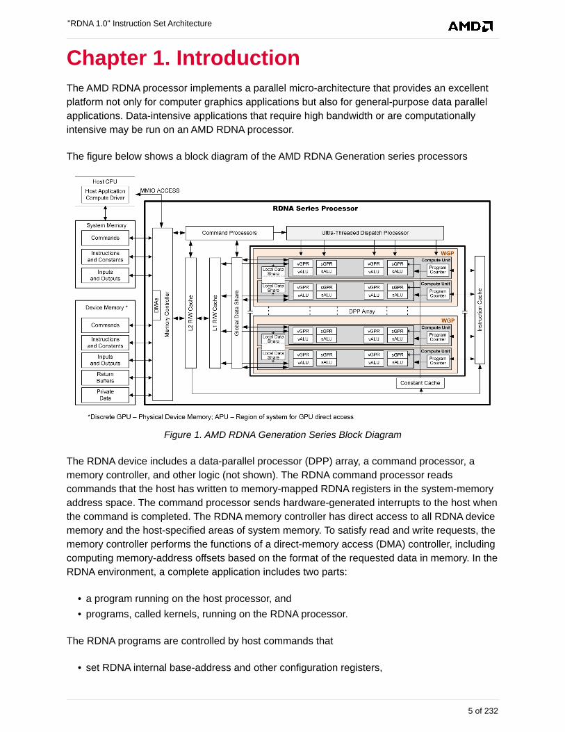
Chapter 1. Introduction
The AMD RDNA processor implements a parallel micro-architecture that provides an excellent
platform not only for computer graphics applications but also for general-purpose data parallel
applications. Data-intensive applications that require high bandwidth or are computationally
intensive may be run on an AMD RDNA processor.
The figure below shows a block diagram of the AMD RDNA Generation series processors
Figure 1. AMD RDNA Generation Series Block Diagram
The RDNA device includes a data-parallel processor (DPP) array, a command processor, a
memory controller, and other logic (not shown). The RDNA command processor reads
commands that the host has written to memory-mapped RDNA registers in the system-memory
address space. The command processor sends hardware-generated interrupts to the host when
the command is completed. The RDNA memory controller has direct access to all RDNA device
memory and the host-specified areas of system memory. To satisfy read and write requests, the
memory controller performs the functions of a direct-memory access (DMA) controller, including
computing memory-address offsets based on the format of the requested data in memory. In the
RDNA environment, a complete application includes two parts:
• a program running on the host processor, and
• programs, called kernels, running on the RDNA processor.
The RDNA programs are controlled by host commands that
• set RDNA internal base-address and other configuration registers,
"RDNA 1.0" Instruction Set Architecture
5 of 232
• specify the data domain on which the RDNA GPU is to operate,
• invalidate and flush caches on the RDNA GPU, and
• cause the RDNA GPU to begin execution of a program.
The RDNA driver program runs on the host.
The DPP array is the heart of the RDNA processor. The array is organized as a set of
workgroup processor pipelines, each independent from the others, that operate in parallel on
streams of floating-point or integer data. The workgroup processor pipelines can process data
or, through the memory controller, transfer data to, or from, memory. Computation in a
workgroup processor pipeline can be made conditional. Outputs written to memory can also be
made conditional.
When it receives a request, the workgroup processor pipeline loads instructions and data from
memory, begins execution, and continues until the end of the kernel. As kernels are running, the
RDNA hardware automatically fetches instructions from memory into on-chip caches; RDNA
software plays no role in this. RDNA kernels can load data from off-chip memory into on-chip
general-purpose registers (GPRs) and caches.
The AMD RDNA devices can detect floating point exceptions and can generate interrupts. In
particular, they detect IEEE floating-point exceptions in hardware; these can be recorded for
post-execution analysis. The software interrupts shown in the previous figure from the command
processor to the host represent hardware-generated interrupts for signaling command-
completion and related management functions.
The RDNA processor hides memory latency by keeping track of potentially hundreds of work-
items in different stages of execution, and by overlapping compute operations with memory-
access operations.
1.1. Terminology
Table 1. Basic Terms
Term Description
RDNA Processor The RDNA shader processor is a scalar and vector ALU designed to run complexprograms on behalf of a wavefront.
Dispatch A dispatch launches a 1D, 2D, or 3D grid of work to the RDNA processor array.
Workgroup A workgroup is a collection of wavefronts that have the ability to synchronize with eachother quickly; they also can share data through the Local Data Share.
Wavefront A collection of 32 or 64 work-items that execute in parallel on a single RDNA processor.
Work-item A single element of work: one element from the dispatch grid, or in graphics a pixel orvertex.
Literal Constant A 32-bit integer or float constant that is placed in the instruction stream.
Scalar ALU (SALU) The scalar ALU operates on one value per wavefront and manages all control flow.
Vector ALU (VALU) The vector ALU maintains Vector GPRs that are unique for each work item and executearithmetic operations uniquely on each work-item.
"RDNA 1.0" Instruction Set Architecture
1.1. Terminology 6 of 232
Term Description
Workgroup Processor(WGP)
The basic unit of shader computation hardware, including scalar & vector ALU’s andmemory, as well as LDS and scalar caches.
Compute Unit (CU) One half of a WGP. Contains 2 SIMD32’s which share one path to memory.
Microcode format The microcode format describes the bit patterns used to encode instructions. Eachinstruction is either 32 or more bits, in units of 32-bits.
Instruction An instruction is the basic unit of the kernel. Instructions include: vector ALU, scalarALU, memory transfer, and control flow operations.
Quad A quad is a 2x2 group of screen-aligned pixels. This is relevant for sampling texturemaps.
Texture Sampler (S#) A texture sampler is a 128-bit entity that describes how the vector memory systemreads and samples (filters) a texture map.
Texture Resource (T#) A texture resource descriptor describes an image in memory: address, data format,stride, etc.
Buffer Resource (V#) A buffer resource descriptor describes a buffer in memory: address, data format, stride,etc.
UTC Universal (Address) Translation Cache : used for virtual memory translating logical tophysical addresses.
"RDNA 1.0" Instruction Set Architecture
1.1. Terminology 7 of 232
Chapter 2. Program Organization
RDNA kernels are programs executed by the RDNA processor. Conceptually, the kernel is
executed independently on every work-item, but in reality the RDNA processor groups 32 or 64
work-items into a wavefront, which executes the kernel on all 32 or 64 work-items in one pass.
The RDNA processor consists of:
• A scalar ALU, which operates on one value per wavefront (common to all work items).
• A vector ALU, which operates on unique values per work-item.
• Local data storage, which allows work-items within a workgroup to communicate and share
data.
• Scalar memory, which can transfer data between SGPRs and memory through a cache.
• Vector memory, which can transfer data between VGPRs and memory, including sampling
texture maps.
All kernel control flow is handled using scalar ALU instructions. This includes if/else, branches
and looping. Scalar ALU (SALU) and memory instructions work on an entire wavefront and
operate on up to two SGPRs, as well as literal constants.
Vector memory and ALU instructions operate on all work-items in the wavefront at one time. In
order to support branching and conditional execute, every wavefront has an EXECute mask that
determines which work-items are active at that moment, and which are dormant. Active work-
items execute the vector instruction, and dormant ones treat the instruction as a NOP. The
EXEC mask can be changed at any time by Scalar ALU instructions.
Vector ALU instructions can take up to three arguments, which can come from VGPRs, SGPRs,
or literal constants that are part of the instruction stream. They operate on all work-items
enabled by the EXEC mask. Vector compare and add with- carryout return a bit-per-work-item
mask back to the SGPRs to indicate, per work-item, which had a "true" result from the compare
or generated a carry-out.
Vector memory instructions transfer data between VGPRs and memory. Each work-item
supplies its own memory address and supplies or receives unique data. These instructions are
also subject to the EXEC mask.
2.1. Wave32 and Wave64
The shader hardware supports both wavefronts of 32 workitems ("wave32") and wavefronts of
64 workitems ("wave64"). Both wave sizes are supported for all operations, but shader
programs must be compiled for a particular wave size. The underlying hardware is primarily
natively wave32, and wave64 vector ALU and memory operations are executed by issuing the
instruction twice: once for the low 32 workitems, and then again for the high 32 workitems.
Either half of the execution of a wave64 may be skipped if there is no work to do for that half
"RDNA 1.0" Instruction Set Architecture
2.1. Wave32 and Wave64 8 of 232
(i.e. EXEC == 0 for that half). Wave64 VALU instructions which return a scalar (SGPR or VCC)
value never skip either pass. Wave64 Vector Memory instructions can skip either pass, but
never skip both passes.
The upper half of EXEC and VCC are ignored for wave32 waves.
2.2. Compute Shaders
Compute kernels (shaders) are generic programs that can run on the RDNA processor, taking
data from memory, processing it, and writing results back to memory. Compute kernels are
created by a dispatch, which causes the RDNA processors to run the kernel over all of the work-
items in a 1D, 2D, or 3D grid of data. The RDNA processor walks through this grid and
generates wavefronts, which then run the compute kernel. Each work-item is initialized with its
unique address (index) within the grid. Based on this index, the work-item computes the
address of the data it is required to work on and what to do with the results.
2.3. Data Sharing
The AMD RDNA stream processors are designed to share data between different work-items.
Data sharing can boost performance. The figure below shows the memory hierarchy that is
available to each work-item.
"RDNA 1.0" Instruction Set Architecture
2.2. Compute Shaders 9 of 232
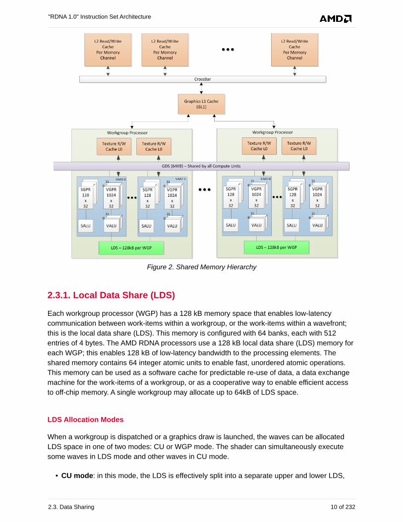
Figure 2. Shared Memory Hierarchy
2.3.1. Local Data Share (LDS)
Each workgroup processor (WGP) has a 128 kB memory space that enables low-latency
communication between work-items within a workgroup, or the work-items within a wavefront;
this is the local data share (LDS). This memory is configured with 64 banks, each with 512
entries of 4 bytes. The AMD RDNA processors use a 128 kB local data share (LDS) memory for
each WGP; this enables 128 kB of low-latency bandwidth to the processing elements. The
shared memory contains 64 integer atomic units to enable fast, unordered atomic operations.
This memory can be used as a software cache for predictable re-use of data, a data exchange
machine for the work-items of a workgroup, or as a cooperative way to enable efficient access
to off-chip memory. A single workgroup may allocate up to 64kB of LDS space.
LDS Allocation Modes
When a workgroup is dispatched or a graphics draw is launched, the waves can be allocated
LDS space in one of two modes: CU or WGP mode. The shader can simultaneously execute
some waves in LDS mode and other waves in CU mode.
• CU mode: in this mode, the LDS is effectively split into a separate upper and lower LDS,
"RDNA 1.0" Instruction Set Architecture
2.3. Data Sharing 10 of 232
each serving two SIMD32’s.
Wave are allocated LDS space within the half of LDS which is associated with the SIMD the
wave is running on.
For workgroups, all waves will be assigned to the pair of SIMD32’s. This mode may provide
faster operation since both halves run in parallel, but limits data sharing
(upper waves cannot read data in the lower half of LDS and vice versa).
When in CU mode, all waves in the workgroup are resident within the same CU.
• WGP mode: in this mode, the LDS is one large contiguous memory that all waves on the
WGP can access.
In WGP mode, waves of a workgroup may be distributed across both CU’s (all 4 SIMD32’s)
in the WGP.
2.3.2. Global Data Share (GDS)
The AMD RDNA devices use a 64 kB global data share (GDS) memory that can be used by
wavefronts of a kernel on all WGPss. This memory provides 128 bytes per cycle of memory
access to all the processing elements. The GDS is configured with 32 banks, each with 512
entries of 4 bytes each. It is designed to provide full access to any location for any processor.
The shared memory contains 32 integer atomic units to enable fast, unordered atomic
operations. This memory can be used as a software cache to store important control data for
compute kernels, reduction operations, or a small global shared surface. Data can be preloaded
from memory prior to kernel launch and written to memory after kernel completion. The GDS
block contains support logic for unordered append/consume and domain launch ordered
append/consume operations to buffers in memory. These dedicated circuits enable fast
compaction of data or the creation of complex data structures in memory.
2.4. Device Memory
The AMD RDNA devices offer several methods for access to off-chip memory from the
processing elements (PE) within each WGP. On the primary read path, the device consists of
multiple channels of L2 cache that provides data to Read-only L1 caches, and finally to L0
caches per WGP. Specific cache-less load instructions can force data to be retrieved from
device memory during an execution of a load clause. Load requests that overlap within the
clause are cached with respect to each other. The output cache is formed by two levels of
cache: the first for write-combining cache (collect scatter and store operations and combine
them to provide good access patterns to memory); the second is a read/write cache with atomic
units that lets each processing element complete unordered atomic accesses that return the
initial value. Each processing element provides the destination address on which the atomic
operation acts, the data to be used in the atomic operation, and a return address for the
read/write atomic unit to store the pre-op value in memory. Each store or atomic operation can
be set up to return an acknowledgment to the requesting PE upon write confirmation of the
return value (pre-atomic op value at destination) being stored to device memory.
This acknowledgment has two purposes:
"RDNA 1.0" Instruction Set Architecture
2.4. Device Memory 11 of 232
• enabling a PE to recover the pre-op value from an atomic operation by performing a cache-
less load from its return address after receipt of the write confirmation acknowledgment,
and
• enabling the system to maintain a relaxed consistency model.
Each scatter write from a given PE to a given memory channel maintains order. The
acknowledgment enables one processing element to implement a fence to maintain serial
consistency by ensuring all writes have been posted to memory prior to completing a
subsequent write. In this manner, the system can maintain a relaxed consistency model
between all parallel work-items operating on the system.
2.5. Shader Padding Requirement
Due to aggressive instruction prefetching used in some graphics devices, all shaders must be
padded out with 64 extra dwords (256 bytes) of data past the end of the shader. It is
recommended to use the S_CODE_END instruction as padding. This ensures that if the
instruction prefetch hardware goes beyond the end of the shader, it will not reach into
uninitialized memory (or unmapped memory pages).
"RDNA 1.0" Instruction Set Architecture
2.5. Shader Padding Requirement 12 of 232
Chapter 3. Kernel State
This chapter describes the kernel states visible to the shader program.
3.1. State Overview
The table below shows all of the hardware states readable or writable by a shader program.
Table 2. Readable and Writable Hardware States
Abbrev. Name Size(bits)
Description
PC Program Counter 48 Points to the memory address of the next shaderinstruction to execute.
V0-V255 VGPR 32 Vector general-purpose register.
S0-S105 SGPR 32 Vector general-purpose register.
LDS Local Data Share 64kB Local data share is a scratch RAM with built-inarithmetic capabilities that allow data to be sharedbetween threads in a workgroup.
EXEC Execute Mask 64 A bit mask with one bit per thread, which is applied tovector instructions and controls that threads executeand that ignore the instruction.
EXECZ EXEC is zero 1 A single bit flag indicating that the EXEC mask is allzeros.
VCC Vector Condition Code 64 A bit mask with one bit per thread; it holds the resultof a vector compare operation.
VCCZ VCC is zero 1 A single bit-flag indicating that the VCC mask is allzeros.
SCC Scalar Condition Code 1 Result from a scalar ALU comparison instruction.
FLAT_SCRATCH Flat scratch address 64 The base address of scratch memory.
XNACK_MASK Address translation failure. 32 Bit mask of threads that have failed their addresstranslation.
STATUS Status 32 Read-only shader status bits.
MODE Mode 32 Writable shader mode bits.
M0 Memory Reg 32 A temporary register that has various uses, includingGPR indexing and bounds checking.
TRAPSTS Trap Status 32 Holds information about exceptions and pendingtraps.
TBA Trap Base Address 64 Holds the pointer to the current trap handler program.
TMA Trap Memory Address 64 Temporary register for shader operations. Forexample, can hold a pointer to memory used by thetrap handler.
TTMP0-TTMP15 Trap Temporary SGPRs 32 16 SGPRs available only to the Trap Handler fortemporary storage.
VMCNT Vector memory instructioncount
6 Counts the number of VMEM load instructions issuedbut not yet completed.
VSCNT Vector memory instructioncount
6 Counts the number of VMEM store instructionsissued but not yet completed.
"RDNA 1.0" Instruction Set Architecture
3.1. State Overview 13 of 232
Abbrev. Name Size(bits)
Description
EXPCNT Export Count 3 Counts the number of Export and GDS instructionsissued but not yet completed. Also counts VMEMwrites that have not yet sent their write-data to thelast level cache.
LGKMCNT LDS, GDS, Constant andMessage count
4 Counts the number of LDS, GDS, constant-fetch(scalar memory read), and message instructionsissued but not yet completed.
3.2. Program Counter (PC)
The program counter (PC) is a byte address pointing to the next instruction to execute. When a
wavefront is created, the PC is initialized to the first instruction in the program.
The PC interacts with three instructions: S_GET_PC, S_SET_PC, S_SWAP_PC. These transfer
the PC to, and from, an even-aligned SGPR pair.
Branches jump to (PC_of_the_instruction_after_the_branch + offset). The shader program
cannot directly read from, or write to, the PC. Branches, GET_PC and SWAP_PC, are PC-
relative to the next instruction, not the current one. S_TRAP saves the PC of the S_TRAP
instruction itself.
3.3. EXECute Mask
The Execute mask (64-bit) determines which threads in the vector are executed:
1 = execute, 0 = do not execute.
EXEC can be read from, and written to, through scalar instructions; it also can be written as a
result of a vector-ALU compare (V_CMPX). This mask affects vector-ALU, vector-memory, LDS,
GDS, and export instructions. It does not affect scalar (ALU or memory) execution or branches.
A helper bit (EXECZ) can be used as a condition for branches to skip code when EXEC is zero.
Wave32: the upper 32-bit of EXEC are ignored, and EXECZ represents the status of only the
lower 32-bits of EXEC.
This GPU can optimize instruction execution when EXEC = 0.
The shader hardware can skip vector ALU and memory instructions if EXEC is known to
be zero, but with some limitations:
• VALU instructions can be skipped, unless they write SGPRs (never skipped)
• Wave64 memory instructions: can skip one half but never entire instruction
• Wave32 memory instructions: never skip
"RDNA 1.0" Instruction Set Architecture
3.2. Program Counter (PC) 14 of 232
Use CBRANCH to rapidly skip over code when it is likely that the EXEC mask is zero.
3.4. Status registers
Status register fields can be read, but not written to, by the shader. These bits are initialized at
wavefront-creation time. The table below lists and briefly describes the status register fields.
Table 3. Status Register Fields
Field BitPosition
Description
SCC 1 Scalar condition code. Used as a carry-out bit. For a comparison instruction,this bit indicates failure or success. For logical operations, this is 1 if theresult was non-zero.
SPI_PRIO 2:1 Wavefront priority set by the shader processor interpolator (SPI) when thewavefront is created. See the S_SETPRIO instruction (page 12-49) fordetails. 0 is lowest, 3 is highest priority.
USER_PRIO 4:3 User settable wave-priority set by the shader program. See theS_SETPRIO instruction (page 12-49) for details.
PRIV 5 Privileged mode. Can only be active when in the trap handler. Gives writeaccess to the TTMP, TMA, and TBA registers.
TRAP_EN 6 Indicates that a trap handler is present. When set to zero, traps are nottaken.
TTRACE_EN 7 Indicates whether thread trace is enabled for this wavefront. If zero, alsoignore any shader-generated (instruction) thread-trace data.
EXPORT_RDY 8 This status bit indicates if export buffer space has been allocated. Theshader stalls any export instruction until this bit becomes 1. It is set to 1when export buffer space has been allocated. Before a Pixel or Vertexshader can export, the hardware checks the state of this bit. If the bit is 1,export can be issued. If the bit is zero, the wavefront sleeps until spacebecomes available in the export buffer. Then, this bit is set to 1, and thewavefront resumes.
EXECZ 9 Exec mask is zero.
VCCZ 10 Vector condition code is zero.
IN_WG 11 Wavefront is a member of a work-group of more than one wavefront.
IN_BARRIER 12 Wavefront is waiting at a barrier.
HALT 13 Wavefront is halted or scheduled to halt. HALT can be set by the hostthrough wavefront-control messages, or by the shader. This bit is ignoredwhile in the trap handler (PRIV = 1); it also is ignored if a host-initiated trapis received (request to enter the trap handler).
TRAP 14 Wavefront is flagged to enter the trap handler as soon as possible.
TTRACE_SIMD_EN 15 Enables/disables thread trace for this SIMD. This bit allows more than oneSIMD to be outputting USERDATA (shader initiated writes to the thread-trace buffer). Note that wavefront data is only traced from one SIMD pershader engine. Wavefront user data (instruction based) can still be output ifthis bit is zero.
VALID 16 Wavefront is active (has been created and not yet ended).
ECC_ERR 17 An ECC error has occurred.
SKIP_EXPORT 18 For Vertex Shaders only. 1 = this shader is never allocated export bufferspace; all export instructions are ignored (treated as NOPs). Formerlycalled VS_NO_ALLOC. Used for stream-out of multiple streams (multiplepasses over the same VS), and for DS running in the VS stage forwavefronts that produced no primitives.
"RDNA 1.0" Instruction Set Architecture
3.4. Status registers 15 of 232
Field BitPosition
Description
PERF_EN 19 Performance counters are enabled for this wavefront.
COND_DBG_USER 20 Conditional debug indicator for user mode
COND_DBG_SYS 21 Conditional debug indicator for system mode.
FATAL_HALT 23 Set if the wave experienced a fatal error.
MUST_EXPORT 27 This wavefront is required to perform an export with Done=1 beforeterminating.
3.5. Mode register
Mode register fields can be read from, and written to, by the shader through scalar instructions.
The table below lists and briefly describes the mode register fields.
Table 4. Mode Register Fields
Field BitPosition
Description
FP_ROUND 3:0 [1:0] Single precision round mode. [3:2] Double/Half-precision round mode.Round Modes: 0=nearest even, 1= +infinity, 2= -infinity, 3= toward zero.
FP_DENORM 7:4 [1:0] Single denormal mode. [3:2] Double/Half-precision denormal mode.Denorm modes:0 = flush input and output denorms.1 = allow input denorms, flush output denorms.2 = flush input denorms, allow output denorms.3 = allow input and output denorms.
DX10_CLAMP 8 Used by the vector ALU to force DX10-style treatment of NaNs: when set,clamp NaN to zero; otherwise, pass NaN through.
IEEE 9 Floating point opcodes that support exception flag gathering quiet andpropagate signaling NaN inputs per IEEE 754-2008. Min_dx10 and max_dx10become IEEE 754-2008 compliant due to signaling NaN propagation andquieting.
LOD_CLAMPED 10 Sticky bit indicating that one or more texture accesses had their LODclamped.
DEBUG 11 Forces the wavefront to jump to the exception handler after each instruction isexecuted (but not after ENDPGM). Only works if TRAP_EN = 1.
EXCP_EN 20:12 Enable mask for exceptions. Enabled means if the exception occurs andTRAP_EN==1, a trap is taken.[12] : invalid.[13] : inputDenormal.[14] : float_div0.[15] : overflow.[16] : underflow.[17] : inexact.[18] : int_div0.[19] : address watch[20] : memory violation
FP16_OVFL 23 If set, an overflowed FP16 result is clamped to +/- MAX_FP16, regardless ofround mode, while still preserving true INF values.
DISABLE_PERF 27 1 = disable performance counting for this wave
"RDNA 1.0" Instruction Set Architecture
3.5. Mode register 16 of 232
3.6. GPRs and LDS
This section describes how GPR and LDS space is allocated to a wavefront, as well as how out-
of-range and misaligned accesses are handled.
3.6.1. Out-of-Range behavior
This section defines the behavior when a source or destination GPR or memory address is
outside the legal range for a wavefront.
Out-of-range can occur through GPR-indexing or bad programming. It is illegal to index from
one register type into another (for example: SGPRs into trap registers or inline constants). It is
also illegal to index within inline constants.
The following describe the out-of-range behavior for various storage types.
• SGPRs
◦ SGPRs cannot be "out of range".
However, it is illegal to index from one range to another, or for a 64-bit operand to
straddle two ranges.
The ranges are: [ SGPRs 0-105 and VCCH, VCCL], [ Trap Temps 0-15 ], [ all other
values ]
• VGPRs
◦ It is illegal to index from SGPRs into VGPRs, or vice versa.
◦ Out-of-range = (vgpr < 0 || (vgpr >= vgpr_size))
◦ If a source VGPR is out of range, VGPR0 is used.
◦ If a destination VGPR is out-of-range, the instruction is ignored and nothing is written
(treated as an NOP).
• LDS
◦ If the LDS-ADDRESS is out-of-range (addr < 0 or > (MIN(lds_size, m0)):
▪ Writes out-of-range are discarded; it is undefined if SIZE is not a multiple of write-
data-size.
▪ Reads return the value zero.
◦ If any source-VGPR is out-of-range, the VGPR0 value is used.
◦ If the dest-VGPR is out of range, nullify the instruction (issue with exec=0)
• Memory, LDS, and GDS: Reads and atomics with returns.
◦ If any source VGPR or SGPR is out-of-range, the data value is undefined.
◦ If any destination VGPR is out-of-range, the operation is nullified by issuing the
instruction as if the EXEC mask were cleared to 0.
▪ This out-of-range check must check all VGPRs that can be returned (for example:
VDST to VDST+3 for a BUFFER_LOAD_DWORDx4).
▪ This check must also include the extra PRT (partially resident texture) VGPR and
nullify the fetch if this VGPR is out-of-range, no matter whether the texture system
"RDNA 1.0" Instruction Set Architecture
3.6. GPRs and LDS 17 of 232
actually returns this value or not.
▪ Atomic operations with out-of-range destination VGPRs are nullified: issued, but
with exec mask of zero.
Instructions with multiple destinations (for example: V_ADDC): if any destination is out-of-range,
no results are written.
3.6.2. SGPR Allocation and storage
Every wavefront is allocated a fixed number of SGPRs:
• 106 normal SGPRs
• VCCh and VCCl (stored in SGPRs 106 and 107)
• 16 Trap-temporary SGPRs, meant for use by the trap handler
3.6.3. SGPR Alignment
Even-aligned SGPRs are required in the following cases.
• When 64-bit data is used. This is required for moves to/from 64-bit registers, including the
PC.
• When scalar memory reads that the address-base comes from an SGPR-pair (either in
SGPR).
Quad-alignment is required for the data-GPR when a scalar memory read returns four or more
Dwords. When a 64-bit quantity is stored in SGPRs, the LSBs are in SGPR[n], and the MSBs
are in SGPR[n+1].
3.6.4. VGPR Allocation and Alignment
VGPRs are allocated in groups of four Dwords for wave64, and 8 Dwords for wave32.
Operations using pairs of VGPRs (for example: double-floats) have no alignment restrictions.
Physically, allocations of VGPRs can wrap around the VGPR memory pool.
3.6.5. Wave Shared VGPRs
Wave64’s can be allocated wave-private and wave-shared VGPRs. Private GPRs are the
normal ones where each lane has a unique value. Shared VGPRS are shared between the high
and low halves of a wave64. This can be useful to reduce overall VGPR usage when combined
with subvector execution. Shared VGPRs are allocated in blocks of 8 Dwords.
Shared VGPRs logically occupy the VGPR addresses immediately following the private VGPRs.
E.g. if a wave has 8 private VGPRs, they are V0-V7 and shared VGPRs start at V8. If there are
"RDNA 1.0" Instruction Set Architecture
3.6. GPRs and LDS 18 of 232
16 shared VGPRs, they are accessed as V8-23.
Shared VGPRs cannot be used for: Exports or GDS.
3.6.6. LDS Allocation and Clamping
LDS is allocated per work-group or per-wavefront when work-groups are not in use. LDS space
is allocated to a work-group or wavefront in contiguous blocks of 128 Dwords on 128-Dword
alignment. LDS allocations do not wrap around the LDS storage. All accesses to LDS are
restricted to the space allocated to that wavefront/work-group.
Clamping of LDS reads and writes is controlled by two size registers, which contain values for
the size of the LDS space allocated by SPI to this wavefront or work-group, and a possibly
smaller value specified in the LDS instruction (size is held in M0). The LDS operations use the
smaller of these two sizes to determine how to clamp the read/write addresses.
3.7. M# Memory Descriptor
There is one 32-bit M# (M0) register per wavefront, which can be used for:
• Local Data Share (LDS)
◦ Interpolation: holds { 1’b0, new_prim_mask[15:1], parameter_offset[15:0] } // in bytes
◦ LDS direct-read offset and data type: { 13’b0, DataType[2:0], LDS_address[15:0] } //
addr in bytes
◦ LDS addressing for Memory/Vfetch → LDS: {16’h0, lds_offset[15:0]} // in bytes
◦ LDS “add_TID” read/write: { 16’h0, lds_offset[15:0] } // offset in bytes
• Global Data Share (GDS)
◦ { base[15:0] , size[15:0] } // base and size are in bytes
• Indirect GPR addressing for both vector and scalar instructions. M0 is an unsigned index.
• Send-message value. EMIT/CUT use M0 and EXEC as the send-message data.
• Index value used by S_MOVREL and V_MOVREL
3.8. SCC: Scalar Condition code
Most scalar ALU instructions set the Scalar Condition Code (SCC) bit, indicating the result of the
operation.
"RDNA 1.0" Instruction Set Architecture
3.7. M# Memory Descriptor 19 of 232
Compare operations: 1 = true
Arithmetic operations: 1 = carry out
Bit/logical operations: 1 = result was not zero
Move: does not alter SCC
The SCC can be used as the carry-in for extended-precision integer arithmetic, as well as the
selector for conditional moves and branches.
3.9. Vector Compares: VCC and VCCZ
Vector ALU comparisons set the Vector Condition Code (VCC) register (1=pass, 0=fail). Also,
vector compares have the option of setting EXEC to the VCC value.
There is also a VCC summary bit (vccz) that is set to 1 when the VCC result is zero. This is
useful for early-exit branch tests. VCC is also set for selected integer ALU operations (carry-
out).
Vector compares have the option of writing the result to VCC (32-bit instruction encoding) or to
any SGPR (64-bit instruction encoding). VCCZ is updated every time VCC is updated: vector
compares and scalar writes to VCC.
The EXEC mask determines which threads execute an instruction. The VCC indicates which
executing threads passed the conditional test, or which threads generated a carry-out from an
integer add or subtract.
V_CMP_* ⇒ VCC[n] = EXEC[n] & (test passed for thread[n])
VCC is fully written; there are no partial mask updates.
VCC physically resides in the SGPR register file, so when an instruction
sources VCC, that counts against the limit on the total number of SGPRs that
can be sourced for a given instruction. VCC physically resides in the highest
two user SGPRs.
When used by a wave32, the upper 32 bits of VCC are unused and only the lower 32 bits of
VCC contribute to the value of VCCZ.
"RDNA 1.0" Instruction Set Architecture
3.9. Vector Compares: VCC and VCCZ 20 of 232
3.10. Trap and Exception registers
Each type of exception can be enabled or disabled independently by setting, or clearing, bits in
the TRAPSTS register’s EXCP_EN field. This section describes the registers which control and
report kernel exceptions.
All Trap temporary SGPRs (TTMP*) are privileged for writes - they can be written only when in
the trap handler (status.priv = 1). When not privileged, writes to these are ignored. TMA and
TBA are read-only; they can be accessed through S_GETREG_B32.
When a trap is taken (either user initiated, exception or host initiated), the shader hardware
generates an S_TRAP instruction. This loads trap information into a pair of SGPRS:
{TTMP1, TTMP0} = {1'h0, pc_rewind[5:0], HT[0],trapID[7:0], PC[47:0]}.
HT is set to one for host initiated traps, and zero for user traps (s_trap) or exceptions. TRAP_ID
is zero for exceptions, or the user/host trapID for those traps. When the trap handler is entered,
the PC of the faulting instruction will be: (PC - PC_rewind*4).
STATUS . TRAP_EN - This bit indicates to the shader whether or not a trap handler is present.
When one is not present, traps are not taken, no matter whether they’re floating point, user-, or
host-initiated traps. When the trap handler is present, the wavefront uses an extra 16 SGPRs for
trap processing. If trap_en == 0, all traps and exceptions are ignored, and s_trap is converted
by hardware to NOP.
MODE . EXCP_EN[8:0] - Floating point exception enables. Defines which exceptions and
events cause a trap.
Bit Exception
0 Invalid
1 Input Denormal
2 Divide by zero
3 Overflow
4 Underflow
5 Inexact
6 Integer divide by zero
7 Address Watch - the cache has witnessed a thread access to an'address of interest'
3.10.1. Trap Status register
The trap status register records previously seen traps or exceptions. It can be read and written
by the kernel.
"RDNA 1.0" Instruction Set Architecture
3.10. Trap and Exception registers 21 of 232
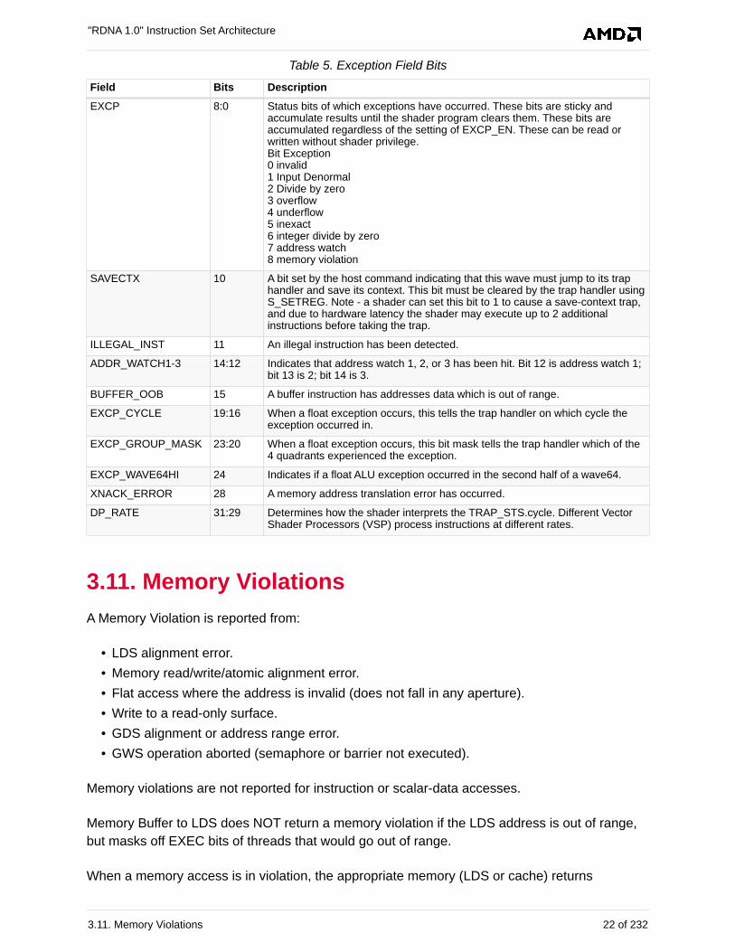
Table 5. Exception Field Bits
Field Bits Description
EXCP 8:0 Status bits of which exceptions have occurred. These bits are sticky andaccumulate results until the shader program clears them. These bits areaccumulated regardless of the setting of EXCP_EN. These can be read orwritten without shader privilege.Bit Exception0 invalid1 Input Denormal2 Divide by zero3 overflow4 underflow5 inexact6 integer divide by zero7 address watch8 memory violation
SAVECTX 10 A bit set by the host command indicating that this wave must jump to its traphandler and save its context. This bit must be cleared by the trap handler usingS_SETREG. Note - a shader can set this bit to 1 to cause a save-context trap,and due to hardware latency the shader may execute up to 2 additionalinstructions before taking the trap.
ILLEGAL_INST 11 An illegal instruction has been detected.
ADDR_WATCH1-3 14:12 Indicates that address watch 1, 2, or 3 has been hit. Bit 12 is address watch 1;bit 13 is 2; bit 14 is 3.
BUFFER_OOB 15 A buffer instruction has addresses data which is out of range.
EXCP_CYCLE 19:16 When a float exception occurs, this tells the trap handler on which cycle theexception occurred in.
EXCP_GROUP_MASK 23:20 When a float exception occurs, this bit mask tells the trap handler which of the4 quadrants experienced the exception.
EXCP_WAVE64HI 24 Indicates if a float ALU exception occurred in the second half of a wave64.
XNACK_ERROR 28 A memory address translation error has occurred.
DP_RATE 31:29 Determines how the shader interprets the TRAP_STS.cycle. Different VectorShader Processors (VSP) process instructions at different rates.
3.11. Memory Violations
A Memory Violation is reported from:
• LDS alignment error.
• Memory read/write/atomic alignment error.
• Flat access where the address is invalid (does not fall in any aperture).
• Write to a read-only surface.
• GDS alignment or address range error.
• GWS operation aborted (semaphore or barrier not executed).
Memory violations are not reported for instruction or scalar-data accesses.
Memory Buffer to LDS does NOT return a memory violation if the LDS address is out of range,
but masks off EXEC bits of threads that would go out of range.
When a memory access is in violation, the appropriate memory (LDS or cache) returns
"RDNA 1.0" Instruction Set Architecture
3.11. Memory Violations 22 of 232
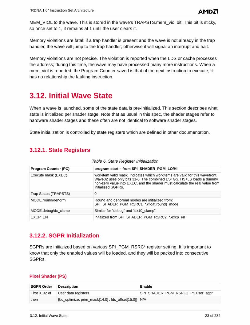
MEM_VIOL to the wave. This is stored in the wave’s TRAPSTS.mem_viol bit. This bit is sticky,
so once set to 1, it remains at 1 until the user clears it.
Memory violations are fatal: if a trap handler is present and the wave is not already in the trap
handler, the wave will jump to the trap handler; otherwise it will signal an interrupt and halt.
Memory violations are not precise. The violation is reported when the LDS or cache processes
the address; during this time, the wave may have processed many more instructions. When a
mem_viol is reported, the Program Counter saved is that of the next instruction to execute; it
has no relationship the faulting instruction.
3.12. Initial Wave State
When a wave is launched, some of the state data is pre-initialized. This section describes what
state is initialized per shader stage. Note that as usual in this spec, the shader stages refer to
hardware shader stages and these often are not identical to software shader stages.
State initialization is controlled by state registers which are defined in other documentation.
3.12.1. State Registers
Table 6. State Register Initialization
Program Counter (PC) program start – from SPI_SHADER_PGM_LO/HI
Execute mask (EXEC) workitem valid mask. Indicates which workitems are valid for this wavefront.Wave32 uses only bits 31-0. The combined ES+GS, HS+LS loads a dummynon-zero value into EXEC, and the shader must calculate the real value frominitialized SGPRs.
Trap Status (TRAPSTS) 0
MODE.round/denorm Round and denormal modes are initialized from:SPI_SHADER_PGM_RSRC1_*.{float,round}_mode
MODE.debug/dx_clamp Similar for "debug" and "dx10_clamp".
EXCP_EN Initalized from SPI_SHADER_PGM_RSRC2_*.excp_en
3.12.2. SGPR Initialization
SGPRs are initialized based on various SPI_PGM_RSRC* register setting. It is important to
know that only the enabled values will be loaded, and they will be packed into consecutive
SGPRs.
Pixel Shader (PS)
SGPR Order Description Enable
First 0..32 of User data registers SPI_SHADER_PGM_RSRC2_PS.user_sgpr
then {bc_optimize, prim_mask[14:0] , lds_offset[15:0]} N/A
"RDNA 1.0" Instruction Set Architecture
3.12. Initial Wave State 23 of 232
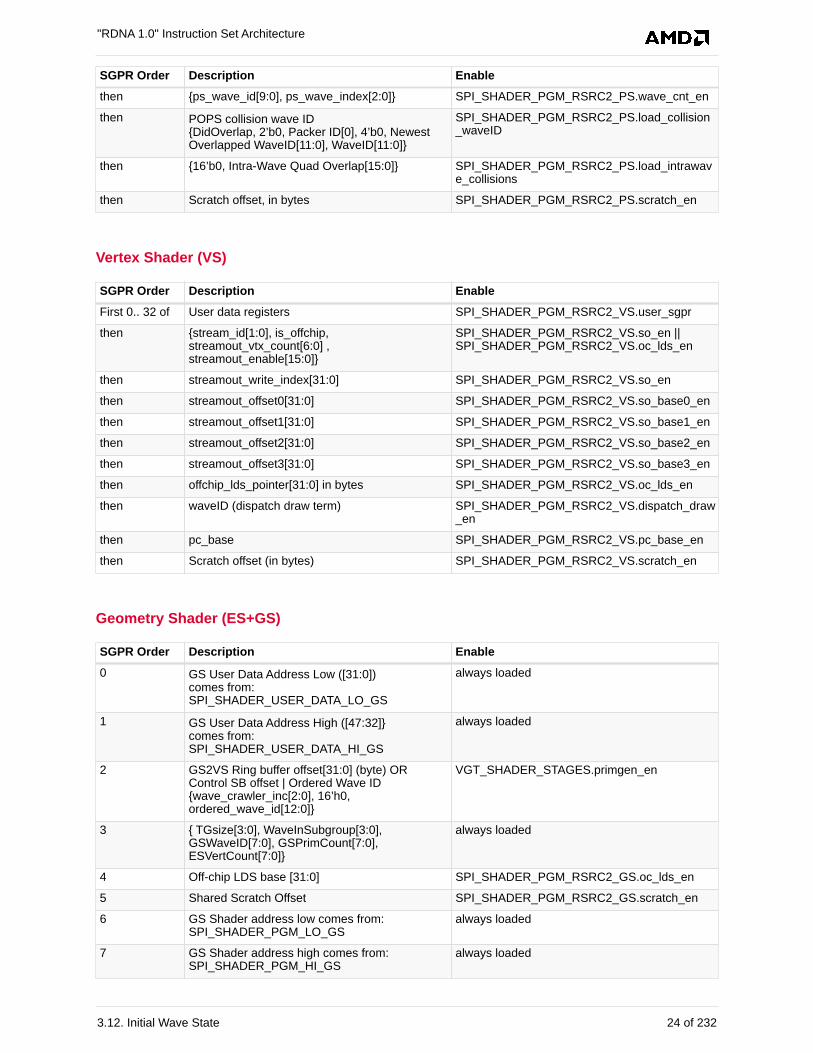
SGPR Order Description Enable
then {ps_wave_id[9:0], ps_wave_index[2:0]} SPI_SHADER_PGM_RSRC2_PS.wave_cnt_en
then POPS collision wave ID{DidOverlap, 2’b0, Packer ID[0], 4’b0, NewestOverlapped WaveID[11:0], WaveID[11:0]}
SPI_SHADER_PGM_RSRC2_PS.load_collision_waveID
then {16’b0, Intra-Wave Quad Overlap[15:0]} SPI_SHADER_PGM_RSRC2_PS.load_intrawave_collisions
then Scratch offset, in bytes SPI_SHADER_PGM_RSRC2_PS.scratch_en
Vertex Shader (VS)
SGPR Order Description Enable
First 0.. 32 of User data registers SPI_SHADER_PGM_RSRC2_VS.user_sgpr
then {stream_id[1:0], is_offchip,streamout_vtx_count[6:0] ,streamout_enable[15:0]}
SPI_SHADER_PGM_RSRC2_VS.so_en ||SPI_SHADER_PGM_RSRC2_VS.oc_lds_en
then streamout_write_index[31:0] SPI_SHADER_PGM_RSRC2_VS.so_en
then streamout_offset0[31:0] SPI_SHADER_PGM_RSRC2_VS.so_base0_en
then streamout_offset1[31:0] SPI_SHADER_PGM_RSRC2_VS.so_base1_en
then streamout_offset2[31:0] SPI_SHADER_PGM_RSRC2_VS.so_base2_en
then streamout_offset3[31:0] SPI_SHADER_PGM_RSRC2_VS.so_base3_en
then offchip_lds_pointer[31:0] in bytes SPI_SHADER_PGM_RSRC2_VS.oc_lds_en
then waveID (dispatch draw term) SPI_SHADER_PGM_RSRC2_VS.dispatch_draw_en
then pc_base SPI_SHADER_PGM_RSRC2_VS.pc_base_en
then Scratch offset (in bytes) SPI_SHADER_PGM_RSRC2_VS.scratch_en
Geometry Shader (ES+GS)
SGPR Order Description Enable
0 GS User Data Address Low ([31:0])comes from:SPI_SHADER_USER_DATA_LO_GS
always loaded
1 GS User Data Address High ([47:32]}comes from:SPI_SHADER_USER_DATA_HI_GS
always loaded
2 GS2VS Ring buffer offset[31:0] (byte) ORControl SB offset | Ordered Wave ID{wave_crawler_inc[2:0], 16’h0,ordered_wave_id[12:0]}
VGT_SHADER_STAGES.primgen_en
3 { TGsize[3:0], WaveInSubgroup[3:0],GSWaveID[7:0], GSPrimCount[7:0],ESVertCount[7:0]}
always loaded
4 Off-chip LDS base [31:0] SPI_SHADER_PGM_RSRC2_GS.oc_lds_en
5 Shared Scratch Offset SPI_SHADER_PGM_RSRC2_GS.scratch_en
6 GS Shader address low comes from:SPI_SHADER_PGM_LO_GS
always loaded
7 GS Shader address high comes from:SPI_SHADER_PGM_HI_GS
always loaded
"RDNA 1.0" Instruction Set Architecture
3.12. Initial Wave State 24 of 232
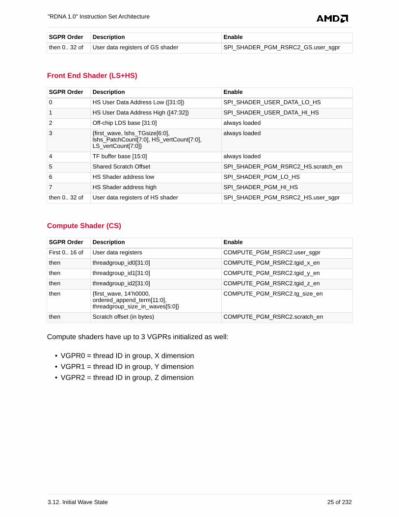
SGPR Order Description Enable
then 0.. 32 of User data registers of GS shader SPI_SHADER_PGM_RSRC2_GS.user_sgpr
Front End Shader (LS+HS)
SGPR Order Description Enable
0 HS User Data Address Low ([31:0]) SPI_SHADER_USER_DATA_LO_HS
1 HS User Data Address High ([47:32]) SPI_SHADER_USER_DATA_HI_HS
2 Off-chip LDS base [31:0] always loaded
3 {first_wave, lshs_TGsize[6:0],lshs_PatchCount[7:0], HS_vertCount[7:0],LS_vertCount[7:0]}
always loaded
4 TF buffer base [15:0] always loaded
5 Shared Scratch Offset SPI_SHADER_PGM_RSRC2_HS.scratch_en
6 HS Shader address low SPI_SHADER_PGM_LO_HS
7 HS Shader address high SPI_SHADER_PGM_HI_HS
then 0.. 32 of User data registers of HS shader SPI_SHADER_PGM_RSRC2_HS.user_sgpr
Compute Shader (CS)
SGPR Order Description Enable
First 0.. 16 of User data registers COMPUTE_PGM_RSRC2.user_sgpr
then threadgroup_id0[31:0] COMPUTE_PGM_RSRC2.tgid_x_en
then threadgroup_id1[31:0] COMPUTE_PGM_RSRC2.tgid_y_en
then threadgroup_id2[31:0] COMPUTE_PGM_RSRC2.tgid_z_en
then {first_wave, 14’h0000,ordered_append_term[11:0],threadgroup_size_in_waves[5:0]}
COMPUTE_PGM_RSRC2.tg_size_en
then Scratch offset (in bytes) COMPUTE_PGM_RSRC2.scratch_en
Compute shaders have up to 3 VGPRs initialized as well:
• VGPR0 = thread ID in group, X dimension
• VGPR1 = thread ID in group, Y dimension
• VGPR2 = thread ID in group, Z dimension
"RDNA 1.0" Instruction Set Architecture
3.12. Initial Wave State 25 of 232
Chapter 4. Program Flow Control
All program flow control is programmed using scalar ALU instructions. This includes loops,
branches, subroutine calls, and traps. The program uses SGPRs to store branch conditions and
loop counters. Constants can be fetched from the scalar constant cache directly into SGPRs.
4.1. Program Control
The instructions in the table below control the priority and termination of a shader program, as
well as provide support for trap handlers.
Table 7. Control Instructions
Instructions Description
S_ENDPGM Terminates the wavefront. It can appear anywhere in the kernel and can appear multipletimes.
S_ENDPGM_SAVED Terminates the wavefront due to context save. It can appear anywhere in the kernel and canappear multiple times.
S_NOP Does nothing; it can be repeated in hardware up to eight times.
S_TRAP Jumps to the trap handler.
S_RFE Returns from the trap handler
S_SETPRIO Modifies the priority of this wavefront: 0=lowest, 3 = highest.
S_SLEEP Causes the wavefront to sleep for 64 - 960 clock cycles.
S_SENDMSG Sends a message (typically an interrupt) to the host CPU.
S_CLAUSE Define a clause of instructions which will be executed together.
S_VERSION Does nothing (treated as S_NOP), but can be used as a code comment to indicate thehardware version the shader is compiled for (using the SIMM16 field).
S_CODE_END Treated as an illegal instruction. Used to pad past the end of shaders.
4.1.1. Instruction Clauses
An instruction clause is a group of instructions of the same type which are to be executed in
an uninterruped sequence. Normally the shader hardware may interleave instructions from
different waves in order to maintain performance, but a clause can be used to override that
behavior and force the hardware to service only one wave for a given instruction type for the
duration of the clause.
Clauses are defined by the S_CLAUSE instructions, which specifies the number of instructions
that make up the clause. The clause-type is implicitly defined by the type of instruction
immediately following the clause. Clause types are:
• VALU
• SMEM
• LDS
"RDNA 1.0" Instruction Set Architecture
4.1. Program Control 26 of 232
• FLAT
• Texture, buffer, global and scratch
Clauses must contain only one instruction type. If a different instruction type is encountered
during the clause, the clause is immediately terminated.
4.2. Branching
Branching is done using one of the following scalar ALU instructions.
Table 8. Branch Instructions
Instructions Description
S_BRANCH Unconditional branch.
S_CBRANCH_<test> Conditional branch. Branch only if <test> is true. Tests are VCCZ, VCCNZ,EXECZ, EXECNZ, SCCZ, and SCCNZ.
S_CBRANCH_CDBGSYS Conditional branch, taken if the COND_DBG_SYS status bit is set.
S_CBRANCH_CDBGUSER Conditional branch, taken if the COND_DBG_USER status bit is set.
S_CBRANCH_CDBGSYS_AND_USER
Conditional branch, taken only if both COND_DBG_SYS andCOND_DBG_USER are set.
S_SETPC Directly set the PC from an SGPR pair.
S_SWAPPC Swap the current PC with an address in an SGPR pair.
S_GETPC Retrieve the current PC value (does not cause a branch).
S_CALL_B64 Jump to a subroutine, and save return address. SGPR_pair = PC+4; PC =PC+4+SIMM16*4.
S_SUBVECTOR_LOOP_BEGIN Starts a subvector execution loop. The SIMM16 field is the branch offset to theinstruction after S_SUBVECTOR_LOOP_END, and the SGPR is used fortemporary EXEC storage.
S_SUBVECTOR_LOOP_END Marks the end of the subvector execution loop. The SIMM16 field points back tothe instruction after S_SUBVECTOR_LOOP_BEGIN, and the SGPR is used fortemporary EXEC storage.
For conditional branches, the branch condition can be determined by either scalar or vector
operations. A scalar compare operation sets the Scalar Condition Code (SCC), which then can
be used as a conditional branch condition. Vector compare operations set the VCC mask, and
VCCZ or VCCNZ then can be used to determine branching.
4.2.1. Subvector Execution
“Subvector execution” is an alternate method of handling wave64 instruction execution. The
normal method is to issue each half of a wave64 as two wave32 instructions, then move on to
the next instruction. This alternative method is to issue a group of instructions, all for the first 32
workitems and then come back and execute the same instructions but for the second 32
workitems. This has two potential advantages:
• Memory operations are for smaller units of work and may cache better
"RDNA 1.0" Instruction Set Architecture
4.2. Branching 27 of 232
◦ example: reading multiple entries from a strided buffer
• Wave-temporary VGPRs are available:
◦ In Wave64 each wave may declare N normal VGPRs (the wave gets 64 * N dwords,
with N per work-item), and M temp VGPRs which may only be used in this mode. The
temp VGPRs are physically adjacent to the normal ones, but logically are from just after
the private VGPRs. These can be used on each pass of the subvector execution.
This mode is explicitly declared in shader code as a loop:
S_subvector_loop_begin S0, skip_allloop_start: < vec32 code > S_subvector_loop_end S0, loop_startskip_all:
Table 9. SubVector Execution Order
ShaderProgram
Normal Execution Sequence Subvector Loop Execution Sequence
inst0inst1inst2inst3
inst0 - lowinst0 - highinst1 - lowinst1 - highinst2 - lowinst2 - highinst3 - lowinst3 – high
inst0 - lowinst1 - lowinst2 - lowinst3 - lowinst0 - highinst1 - highinst2 - highinst3 – high
Subvector execution is simply a loop construct where half of the EXEC mask is zero for each
pass over the body of the code. All wave64 rules still apply. The loop will execute zero, one or
two times, depending on the initial state of the EXEC mask. During each pass of the loop, one
half of EXEC is forced to zero (after being saved in an SGPR). The EXEC mask is restored at
the end of the loop.
If EXECHI = 0: the body is executed only once: EXECLO is stored in S0 and restored at the
end, but it was zero anyway. If EXEC_LO was zero at the start, the same thing happens. If both
halves of EXEC are non-zero, do the low pass first (storing EXECHI in S0), then restore
EXECHI and save off EXECLO and do it again. Restore EXECLO at the end of the second
pass. The “pass #” is encoded by observing which half of EXEC is zero.
Subvector looping imposes a rule that the “body code” cannot let the working half of the exec
mask go to zero. If it might go to zero, it must be saved at the start of the loop and be restored
before the end since the S_SUBVECTOR_LOOP_* instructions determine which pass they’re in
by looking at which half of EXEC is zero.
"RDNA 1.0" Instruction Set Architecture
4.2. Branching 28 of 232
4.3. Workgroups
Work-groups are collections of wavefronts running on the same workgroup processor which can
synchronize and share data. Up to 1024 work-items (16 wave64’s or 32 wave32’s) can be
combined into a work-group. When multiple wavefronts are in a workgroup, the S_BARRIER
instruction can be used to force each wavefront to wait until all other wavefronts reach the same
instruction; then, all wavefronts continue. Any wavefront may terminate early using S_ENDPGM,
and the barrier is considered satisfied when the remaining live waves reach their barrier
instruction.
4.4. Data Dependency Resolution
Shader hardware resolves most data dependencies, but a few cases must be explicitly handled
by the shader program. In these cases, the program must insert S_WAITCNT instructions to
ensure that previous operations have completed before continuing.
The shader has four counters that track the progress of issued instructions. S_WAITCNT waits
for the values of these counters to be at, or below, specified values before continuing.
These allow the shader writer to schedule long-latency instructions, execute unrelated work,
and specify when results of long-latency operations are needed.
Instructions of a given type return in order, but instructions of different types can complete out-
of-order. For example, both GDS and LDS instructions use LGKM_cnt, but they can return out-
of-order. VMEM loads return in the order they were issued, but loads and stores are unordered
with each other.
VM_CNT
Vector memory count (reads, atomic with return). Determines when memory reads have
returned data to VGPRs.
• Incremented every time a vector-memory read or atomic-with-return (MIMG, MUBUF,
MTBUF, or FLAT/Scratch/Global format) instruction is issued.
• Decremented for reads when the data has been written back to the VGPRs.
VS_CNT
Vector memory store count (writes, atomic without return). Determines when memory writes
have completed.
• Incremented every time a vector-memory write or atomic-without-return (MIMG, MUBUF,
MTBUF, or Flat/Scratch/Global format) instruction is issued.
• Decremented for writes when the data has been written to the L2 cache.
"RDNA 1.0" Instruction Set Architecture
4.3. Workgroups 29 of 232
LGKM_CNT
(LDS, GDS, (K)constant, (M)essage) Determines when one of these low-latency instructions
have completed.
• Incremented by 1 for every LDS or GDS instruction issued, as well as by Dword-count
for scalar-memory reads. For example, s_memtime counts the same as an
s_load_dwordx2.
• Decremented by 1 for LDS/GDS reads or atomic-with-return when the data has been
returned to VGPRs.
• Incremented by 1 for each S_SENDMSG issued. Decremented by 1 when message is
sent out.
• Decremented by 1 for LDS/GDS writes when the data has been written to LDS/GDS.
• Decremented by 1 for each Dword returned from the data-cache (SMEM).
Ordering:
◦ Instructions of different types are returned out-of-order.
◦ Instructions of the same type are returned in the order they were issued, except
scalar-memory-reads, which can return out-of-order (in which case only
S_WAITCNT 0 is the only legitimate value).
EXP_CNT
VGPR-export count. Determines when data has been read out of the VGPR and sent to
GDS, at which time it is safe to overwrite the contents of that VGPR.
• Incremented when an Export/GDS instruction is issued from the wavefront buffer.
• Decremented for exports/GDS when the last cycle of the export instruction is granted
and executed (VGPRs read out). Ordering
◦ Exports are kept in order only within each export type (color/null, position,
parameter cache).
4.5. Manually Inserted Wait States (NOPs)
Inserting S_NOP is never required to achieve correct operation.
"RDNA 1.0" Instruction Set Architecture
4.5. Manually Inserted Wait States (NOPs) 30 of 232
Chapter 5. Scalar ALU Operations
Scalar ALU (SALU) instructions operate on a single value per wavefront. These operations
consist of 32-bit integer arithmetic and 32- or 64-bit bit-wise operations. The SALU also can
perform operations directly on the Program Counter, allowing the program to create a call stack
in SGPRs. Many operations also set the Scalar Condition Code bit (SCC) to indicate the result
of a comparison, a carry-out, or whether the instruction result was zero.
5.1. SALU Instruction Formats
SALU instructions are encoded in one of five microcode formats, shown below:
Figure 3. Scalar ALU format with one source operand
Figure 4. Scalar ALU format with two source operands
Figure 5. Scalar ALU format with one immediate value source operands
Figure 6. Scalar ALU format for compares, with two sources but no destinaton
Figure 7. Scalar ALU format for program flow operations
Each of these instruction formats uses some of these fields:
Field Description
OP Opcode: instruction to be executed.
SDST Destination SGPR.
SSRC0 First source operand.
SSRC1 Second source operand.
SIMM16 Signed immediate 16-bit integer constant.
The lists of similar instructions sometimes use a condensed form using curly braces { } to
express a list of possible names. For example, S_AND_{B32, B64} defines two legal
instructions: S_AND_B32 and S_AND_B64.
"RDNA 1.0" Instruction Set Architecture
5.1. SALU Instruction Formats 31 of 232
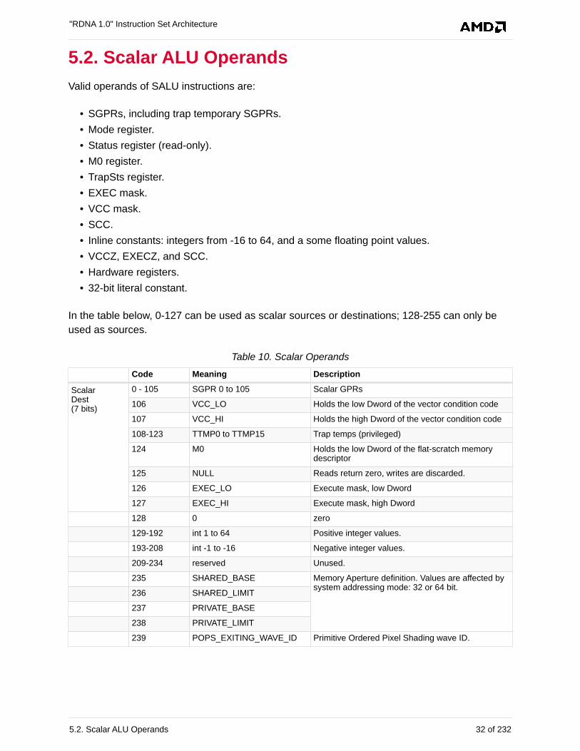
5.2. Scalar ALU Operands
Valid operands of SALU instructions are:
• SGPRs, including trap temporary SGPRs.
• Mode register.
• Status register (read-only).
• M0 register.
• TrapSts register.
• EXEC mask.
• VCC mask.
• SCC.
• Inline constants: integers from -16 to 64, and a some floating point values.
• VCCZ, EXECZ, and SCC.
• Hardware registers.
• 32-bit literal constant.
In the table below, 0-127 can be used as scalar sources or destinations; 128-255 can only be
used as sources.
Table 10. Scalar Operands
Code Meaning Description
ScalarDest(7 bits)
0 - 105 SGPR 0 to 105 Scalar GPRs
106 VCC_LO Holds the low Dword of the vector condition code
107 VCC_HI Holds the high Dword of the vector condition code
108-123 TTMP0 to TTMP15 Trap temps (privileged)
124 M0 Holds the low Dword of the flat-scratch memorydescriptor
125 NULL Reads return zero, writes are discarded.
126 EXEC_LO Execute mask, low Dword
127 EXEC_HI Execute mask, high Dword
128 0 zero
129-192 int 1 to 64 Positive integer values.
193-208 int -1 to -16 Negative integer values.
209-234 reserved Unused.
235 SHARED_BASE Memory Aperture definition. Values are affected bysystem addressing mode: 32 or 64 bit.
236 SHARED_LIMIT
237 PRIVATE_BASE
238 PRIVATE_LIMIT
239 POPS_EXITING_WAVE_ID Primitive Ordered Pixel Shading wave ID.
"RDNA 1.0" Instruction Set Architecture
5.2. Scalar ALU Operands 32 of 232
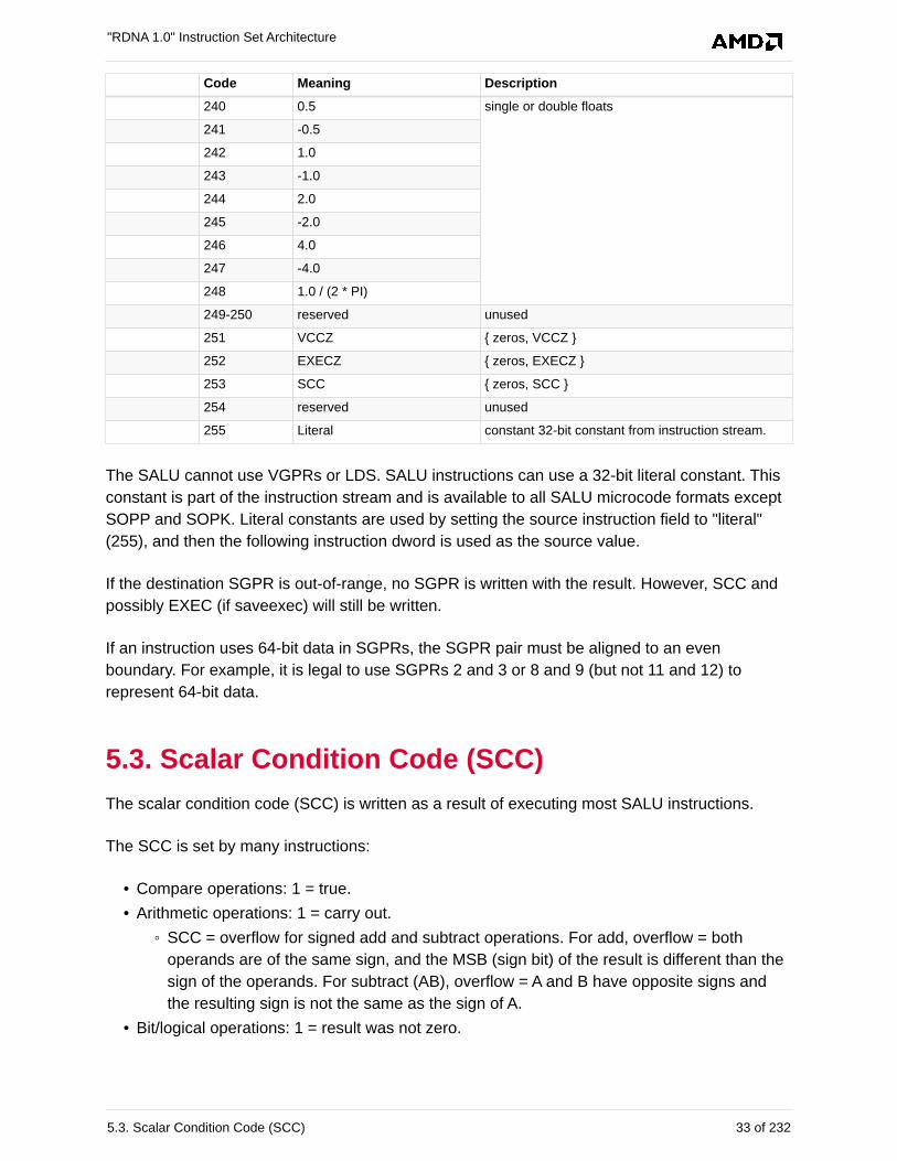
Code Meaning Description
240 0.5 single or double floats
241 -0.5
242 1.0
243 -1.0
244 2.0
245 -2.0
246 4.0
247 -4.0
248 1.0 / (2 * PI)
249-250 reserved unused
251 VCCZ { zeros, VCCZ }
252 EXECZ { zeros, EXECZ }
253 SCC { zeros, SCC }
254 reserved unused
255 Literal constant 32-bit constant from instruction stream.
The SALU cannot use VGPRs or LDS. SALU instructions can use a 32-bit literal constant. This
constant is part of the instruction stream and is available to all SALU microcode formats except
SOPP and SOPK. Literal constants are used by setting the source instruction field to "literal"
(255), and then the following instruction dword is used as the source value.
If the destination SGPR is out-of-range, no SGPR is written with the result. However, SCC and
possibly EXEC (if saveexec) will still be written.
If an instruction uses 64-bit data in SGPRs, the SGPR pair must be aligned to an even
boundary. For example, it is legal to use SGPRs 2 and 3 or 8 and 9 (but not 11 and 12) to
represent 64-bit data.
5.3. Scalar Condition Code (SCC)
The scalar condition code (SCC) is written as a result of executing most SALU instructions.
The SCC is set by many instructions:
• Compare operations: 1 = true.
• Arithmetic operations: 1 = carry out.
◦ SCC = overflow for signed add and subtract operations. For add, overflow = both
operands are of the same sign, and the MSB (sign bit) of the result is different than the
sign of the operands. For subtract (AB), overflow = A and B have opposite signs and
the resulting sign is not the same as the sign of A.
• Bit/logical operations: 1 = result was not zero.
"RDNA 1.0" Instruction Set Architecture
5.3. Scalar Condition Code (SCC) 33 of 232
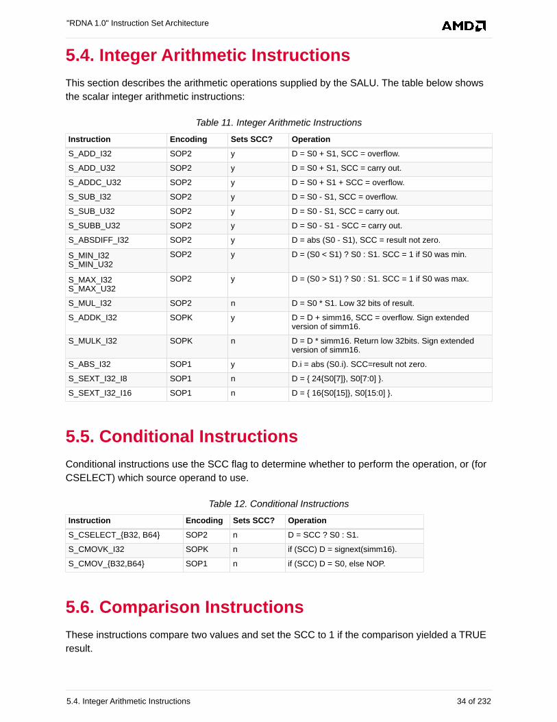
5.4. Integer Arithmetic Instructions
This section describes the arithmetic operations supplied by the SALU. The table below shows
the scalar integer arithmetic instructions:
Table 11. Integer Arithmetic Instructions
Instruction Encoding Sets SCC? Operation
S_ADD_I32 SOP2 y D = S0 + S1, SCC = overflow.
S_ADD_U32 SOP2 y D = S0 + S1, SCC = carry out.
S_ADDC_U32 SOP2 y D = S0 + S1 + SCC = overflow.
S_SUB_I32 SOP2 y D = S0 - S1, SCC = overflow.
S_SUB_U32 SOP2 y D = S0 - S1, SCC = carry out.
S_SUBB_U32 SOP2 y D = S0 - S1 - SCC = carry out.
S_ABSDIFF_I32 SOP2 y D = abs (S0 - S1), SCC = result not zero.
S_MIN_I32S_MIN_U32
SOP2 y D = (S0 < S1) ? S0 : S1. SCC = 1 if S0 was min.
S_MAX_I32S_MAX_U32
SOP2 y D = (S0 > S1) ? S0 : S1. SCC = 1 if S0 was max.
S_MUL_I32 SOP2 n D = S0 * S1. Low 32 bits of result.
S_ADDK_I32 SOPK y D = D + simm16, SCC = overflow. Sign extendedversion of simm16.
S_MULK_I32 SOPK n D = D * simm16. Return low 32bits. Sign extendedversion of simm16.
S_ABS_I32 SOP1 y D.i = abs (S0.i). SCC=result not zero.
S_SEXT_I32_I8 SOP1 n D = { 24{S0[7]}, S0[7:0] }.
S_SEXT_I32_I16 SOP1 n D = { 16{S0[15]}, S0[15:0] }.
5.5. Conditional Instructions
Conditional instructions use the SCC flag to determine whether to perform the operation, or (for
CSELECT) which source operand to use.
Table 12. Conditional Instructions
Instruction Encoding Sets SCC? Operation
S_CSELECT_{B32, B64} SOP2 n D = SCC ? S0 : S1.
S_CMOVK_I32 SOPK n if (SCC) D = signext(simm16).
S_CMOV_{B32,B64} SOP1 n if (SCC) D = S0, else NOP.
5.6. Comparison Instructions
These instructions compare two values and set the SCC to 1 if the comparison yielded a TRUE
result.
"RDNA 1.0" Instruction Set Architecture
5.4. Integer Arithmetic Instructions 34 of 232
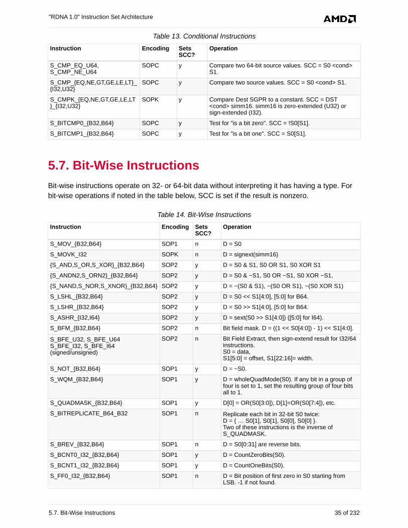
Table 13. Conditional Instructions
Instruction Encoding SetsSCC?
Operation
S_CMP_EQ_U64,S_CMP_NE_U64
SOPC y Compare two 64-bit source values. SCC = S0 <cond>S1.
S_CMP_{EQ,NE,GT,GE,LE,LT}_{I32,U32}
SOPC y Compare two source values. SCC = S0 <cond> S1.
S_CMPK_{EQ,NE,GT,GE,LE,LT}_{I32,U32}
SOPK y Compare Dest SGPR to a constant. SCC = DST<cond> simm16. simm16 is zero-extended (U32) orsign-extended (I32).
S_BITCMP0_{B32,B64} SOPC y Test for "is a bit zero". SCC = !S0[S1].
S_BITCMP1_{B32,B64} SOPC y Test for "is a bit one". SCC = S0[S1].
5.7. Bit-Wise Instructions
Bit-wise instructions operate on 32- or 64-bit data without interpreting it has having a type. For
bit-wise operations if noted in the table below, SCC is set if the result is nonzero.
Table 14. Bit-Wise Instructions
Instruction Encoding SetsSCC?
Operation
S_MOV_{B32,B64} SOP1 n D = S0
S_MOVK_I32 SOPK n D = signext(simm16)
{S_AND,S_OR,S_XOR}_{B32,B64} SOP2 y D = S0 & S1, S0 OR S1, S0 XOR S1
{S_ANDN2,S_ORN2}_{B32,B64} SOP2 y D = S0 & ~S1, S0 OR ~S1, S0 XOR ~S1,
{S_NAND,S_NOR,S_XNOR}_{B32,B64} SOP2 y D = ~(S0 & S1), ~(S0 OR S1), ~(S0 XOR S1)
S_LSHL_{B32,B64} SOP2 y D = S0 << S1[4:0], [5:0] for B64.
S_LSHR_{B32,B64} SOP2 y D = S0 >> S1[4:0], [5:0] for B64.
S_ASHR_{I32,I64} SOP2 y D = sext(S0 >> S1[4:0]) ([5:0] for I64).
S_BFM_{B32,B64} SOP2 n Bit field mask. D = ((1 << S0[4:0]) - 1) << S1[4:0].
S_BFE_U32, S_BFE_U64S_BFE_I32, S_BFE_I64(signed/unsigned)
SOP2 n Bit Field Extract, then sign-extend result for I32/64instructions.S0 = data,S1[5:0] = offset, S1[22:16]= width.
S_NOT_{B32,B64} SOP1 y D = ~S0.
S_WQM_{B32,B64} SOP1 y D = wholeQuadMode(S0). If any bit in a group offour is set to 1, set the resulting group of four bitsall to 1.
S_QUADMASK_{B32,B64} SOP1 y D[0] = OR(S0[3:0]), D[1]=OR(S0[7:4]), etc.
S_BITREPLICATE_B64_B32 SOP1 n Replicate each bit in 32-bit S0 twice:D = { … S0[1], S0[1], S0[0], S0[0] }.Two of these instructions is the inverse ofS_QUADMASK.
S_BREV_{B32,B64} SOP1 n D = S0[0:31] are reverse bits.
S_BCNT0_I32_{B32,B64} SOP1 y D = CountZeroBits(S0).
S_BCNT1_I32_{B32,B64} SOP1 y D = CountOneBits(S0).
S_FF0_I32_{B32,B64} SOP1 n D = Bit position of first zero in S0 starting fromLSB. -1 if not found.
"RDNA 1.0" Instruction Set Architecture
5.7. Bit-Wise Instructions 35 of 232
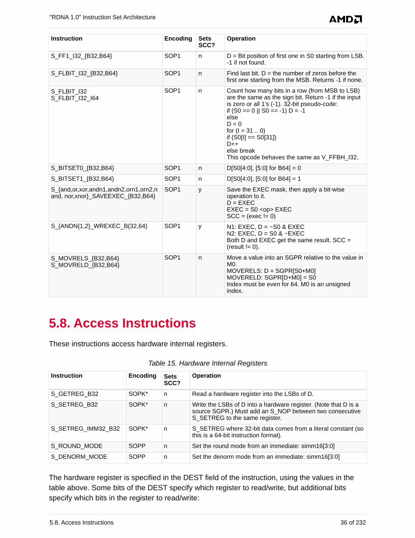
Instruction Encoding SetsSCC?
Operation
S_FF1_I32_{B32,B64} SOP1 n D = Bit position of first one in S0 starting from LSB.-1 if not found.
S_FLBIT_I32_{B32,B64} SOP1 n Find last bit. D = the number of zeros before thefirst one starting from the MSB. Returns -1 if none.
S_FLBIT_I32S_FLBIT_I32_I64
SOP1 n Count how many bits in a row (from MSB to LSB)are the same as the sign bit. Return -1 if the inputis zero or all 1’s (-1). 32-bit pseudo-code:if (S0 == 0 || S0 == -1) D = -1elseD = 0for (I = 31 .. 0)if (S0[I] == S0[31])D++else breakThis opcode behaves the same as V_FFBH_I32.
S_BITSET0_{B32,B64} SOP1 n D[S0[4:0], [5:0] for B64] = 0
S_BITSET1_{B32,B64} SOP1 n D[S0[4:0], [5:0] for B64] = 1
S_{and,or,xor,andn1,andn2,orn1,orn2,nand, nor,xnor}_SAVEEXEC_{B32,B64}
SOP1 y Save the EXEC mask, then apply a bit-wiseoperation to it.D = EXECEXEC = S0 <op> EXECSCC = (exec != 0)
S_{ANDN{1,2}_WREXEC_B{32,64} SOP1 y N1: EXEC, D = ~S0 & EXECN2: EXEC, D = S0 & ~EXECBoth D and EXEC get the same result. SCC =(result != 0).
S_MOVRELS_{B32,B64}S_MOVRELD_{B32,B64}
SOP1 n Move a value into an SGPR relative to the value inM0.MOVERELS: D = SGPR[S0+M0]MOVERELD: SGPR[D+M0] = S0 Index must be even for 64. M0 is an unsignedindex.
5.8. Access Instructions
These instructions access hardware internal registers.
Table 15. Hardware Internal Registers
Instruction Encoding SetsSCC?
Operation
S_GETREG_B32 SOPK* n Read a hardware register into the LSBs of D.
S_SETREG_B32 SOPK* n Write the LSBs of D into a hardware register. (Note that D is asource SGPR.) Must add an S_NOP between two consecutiveS_SETREG to the same register.
S_SETREG_IMM32_B32 SOPK* n S_SETREG where 32-bit data comes from a literal constant (sothis is a 64-bit instruction format).
S_ROUND_MODE SOPP n Set the round mode from an immediate: simm16[3:0]
S_DENORM_MODE SOPP n Set the denorm mode from an immediate: simm16[3:0]
The hardware register is specified in the DEST field of the instruction, using the values in the
table above. Some bits of the DEST specify which register to read/write, but additional bits
specify which bits in the register to read/write:
"RDNA 1.0" Instruction Set Architecture
5.8. Access Instructions 36 of 232
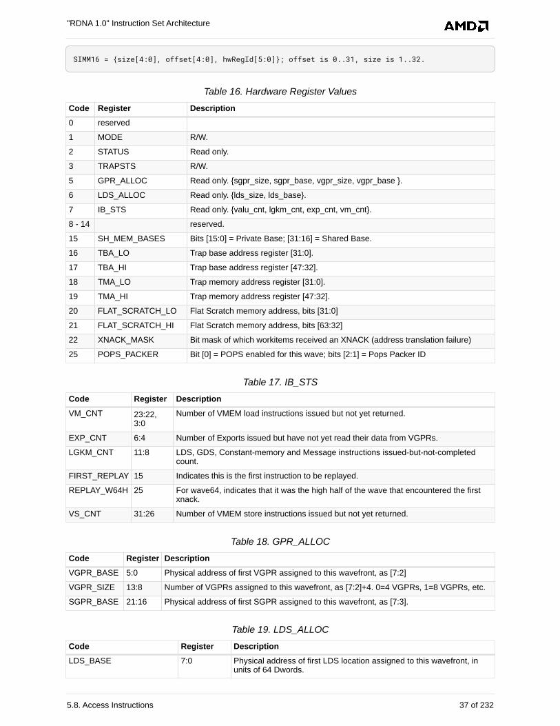
SIMM16 = {size[4:0], offset[4:0], hwRegId[5:0]}; offset is 0..31, size is 1..32.
Table 16. Hardware Register Values
Code Register Description
0 reserved
1 MODE R/W.
2 STATUS Read only.
3 TRAPSTS R/W.
5 GPR_ALLOC Read only. {sgpr_size, sgpr_base, vgpr_size, vgpr_base }.
6 LDS_ALLOC Read only. {lds_size, lds_base}.
7 IB_STS Read only. {valu_cnt, lgkm_cnt, exp_cnt, vm_cnt}.
8 - 14 reserved.
15 SH_MEM_BASES Bits [15:0] = Private Base; [31:16] = Shared Base.
16 TBA_LO Trap base address register [31:0].
17 TBA_HI Trap base address register [47:32].
18 TMA_LO Trap memory address register [31:0].
19 TMA_HI Trap memory address register [47:32].
20 FLAT_SCRATCH_LO Flat Scratch memory address, bits [31:0]
21 FLAT_SCRATCH_HI Flat Scratch memory address, bits [63:32]
22 XNACK_MASK Bit mask of which workitems received an XNACK (address translation failure)
25 POPS_PACKER Bit [0] = POPS enabled for this wave; bits [2:1] = Pops Packer ID
Table 17. IB_STS
Code Register Description
VM_CNT 23:22,3:0
Number of VMEM load instructions issued but not yet returned.
EXP_CNT 6:4 Number of Exports issued but have not yet read their data from VGPRs.
LGKM_CNT 11:8 LDS, GDS, Constant-memory and Message instructions issued-but-not-completedcount.
FIRST_REPLAY 15 Indicates this is the first instruction to be replayed.
REPLAY_W64H 25 For wave64, indicates that it was the high half of the wave that encountered the firstxnack.
VS_CNT 31:26 Number of VMEM store instructions issued but not yet returned.
Table 18. GPR_ALLOC
Code Register Description
VGPR_BASE 5:0 Physical address of first VGPR assigned to this wavefront, as [7:2]
VGPR_SIZE 13:8 Number of VGPRs assigned to this wavefront, as [7:2]+4. 0=4 VGPRs, 1=8 VGPRs, etc.
SGPR_BASE 21:16 Physical address of first SGPR assigned to this wavefront, as [7:3].
Table 19. LDS_ALLOC
Code Register Description
LDS_BASE 7:0 Physical address of first LDS location assigned to this wavefront, inunits of 64 Dwords.
"RDNA 1.0" Instruction Set Architecture
5.8. Access Instructions 37 of 232
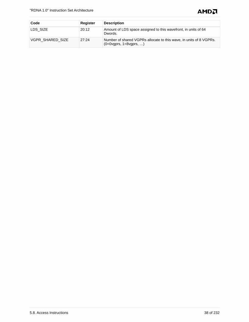
Code Register Description
LDS_SIZE 20:12 Amount of LDS space assigned to this wavefront, in units of 64Dwords.
VGPR_SHARED_SIZE 27:24 Number of shared VGPRs allocate to this wave, in units of 8 VGPRs.(0=0vgprs, 1=8vgprs, …)
"RDNA 1.0" Instruction Set Architecture
5.8. Access Instructions 38 of 232
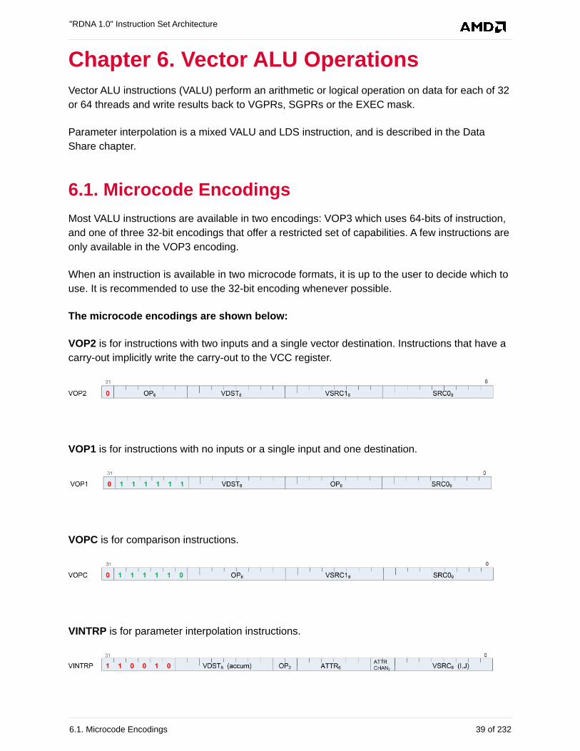
Chapter 6. Vector ALU Operations
Vector ALU instructions (VALU) perform an arithmetic or logical operation on data for each of 32
or 64 threads and write results back to VGPRs, SGPRs or the EXEC mask.
Parameter interpolation is a mixed VALU and LDS instruction, and is described in the Data
Share chapter.
6.1. Microcode Encodings
Most VALU instructions are available in two encodings: VOP3 which uses 64-bits of instruction,
and one of three 32-bit encodings that offer a restricted set of capabilities. A few instructions are
only available in the VOP3 encoding.
When an instruction is available in two microcode formats, it is up to the user to decide which to
use. It is recommended to use the 32-bit encoding whenever possible.
The microcode encodings are shown below:
VOP2 is for instructions with two inputs and a single vector destination. Instructions that have a
carry-out implicitly write the carry-out to the VCC register.
VOP1 is for instructions with no inputs or a single input and one destination.
VOPC is for comparison instructions.
VINTRP is for parameter interpolation instructions.
"RDNA 1.0" Instruction Set Architecture
6.1. Microcode Encodings 39 of 232
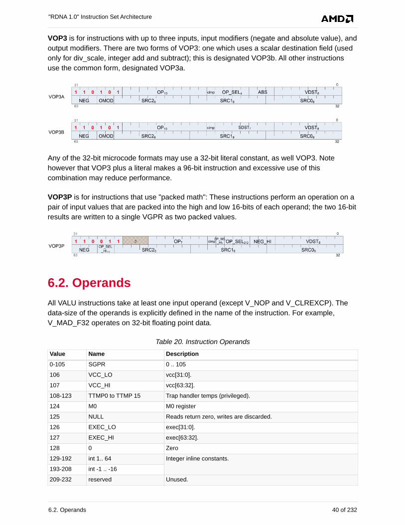
VOP3 is for instructions with up to three inputs, input modifiers (negate and absolute value), and
output modifiers. There are two forms of VOP3: one which uses a scalar destination field (used
only for div_scale, integer add and subtract); this is designated VOP3b. All other instructions
use the common form, designated VOP3a.
Any of the 32-bit microcode formats may use a 32-bit literal constant, as well VOP3. Note
however that VOP3 plus a literal makes a 96-bit instruction and excessive use of this
combination may reduce performance.
VOP3P is for instructions that use "packed math": These instructions perform an operation on a
pair of input values that are packed into the high and low 16-bits of each operand; the two 16-bit
results are written to a single VGPR as two packed values.
6.2. Operands
All VALU instructions take at least one input operand (except V_NOP and V_CLREXCP). The
data-size of the operands is explicitly defined in the name of the instruction. For example,
V_MAD_F32 operates on 32-bit floating point data.
Table 20. Instruction Operands
Value Name Description
0-105 SGPR 0 .. 105
106 VCC_LO vcc[31:0].
107 VCC_HI vcc[63:32].
108-123 TTMP0 to TTMP 15 Trap handler temps (privileged).
124 M0 M0 register
125 NULL Reads return zero, writes are discarded.
126 EXEC_LO exec[31:0].
127 EXEC_HI exec[63:32].
128 0 Zero
129-192 int 1.. 64 Integer inline constants.
193-208 int -1 .. -16
209-232 reserved Unused.
"RDNA 1.0" Instruction Set Architecture
6.2. Operands 40 of 232
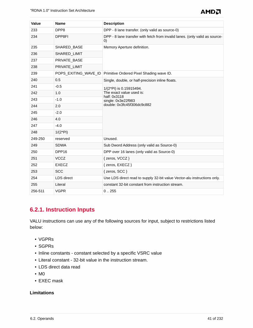
Value Name Description
233 DPP8 DPP - 8 lane transfer. (only valid as source-0)
234 DPP8FI DPP - 8 lane transfer with fetch from invalid lanes. (only valid as source-0)
235 SHARED_BASE Memory Aperture definition.
236 SHARED_LIMIT
237 PRIVATE_BASE
238 PRIVATE_LIMIT
239 POPS_EXITING_WAVE_ID Primitive Ordered Pixel Shading wave ID.
240 0.5 Single, double, or half-precision inline floats.
1/(2*PI) is 0.15915494.The exact value used is:half: 0x3118single: 0x3e22f983double: 0x3fc45f306dc9c882
241 -0.5
242 1.0
243 -1.0
244 2.0
245 -2.0
246 4.0
247 -4.0
248 1/(2*PI)
249-250 reserved Unused.
249 SDWA Sub Dword Address (only valid as Source-0)
250 DPP16 DPP over 16 lanes (only valid as Source-0)
251 VCCZ { zeros, VCCZ }
252 EXECZ { zeros, EXECZ }
253 SCC { zeros, SCC }
254 LDS direct Use LDS direct read to supply 32-bit value Vector-alu instructions only.
255 Literal constant 32-bit constant from instruction stream.
256-511 VGPR 0 .. 255
6.2.1. Instruction Inputs
VALU instructions can use any of the following sources for input, subject to restrictions listed
below:
• VGPRs
• SGPRs
• Inline constants - constant selected by a specific VSRC value
• Literal constant - 32-bit value in the instruction stream.
• LDS direct data read
• M0
• EXEC mask
Limitations
"RDNA 1.0" Instruction Set Architecture
6.2. Operands 41 of 232
• At most two scalar values can be read per instructions, but the values can be used for more
than one operand.
◦ Scalar values include: SGPRs, VCC, EXEC (used as data), and literal constants
◦ Some instructions implicitly read an SGPR (which includes VCC), and this implicit read
counts agains the total supported limit.
▪ These are: Add/sub with carry-in, FMAS and CNDMASK
◦ 64-bit shift instructions can use only a single scalar value, not two
• At most one literal constant can be used
• Inline constants are free, and do not count against these limits
• Only SRC0 can use LDS_DIRECT (see Chapter 10, "Data Share Operations")
Instructions using the VOP3 form and also using floating-point inputs have the option of
applying absolute value (ABS field) or negate (NEG field) to any of the input operands.
Literal Expansion to 64 bits
Literal constants are 32-bits, but they can be used as sources which normally require 64-bit
data. They are expanded to 64 bits following these rules:
• 64 bit float: the lower 32-bit are padded with zero.
• 64-bit unsigned integer: zero extended to 64 bits
• 64-bit signed integer: sign extended to 64 bits
6.2.2. Instruction Outputs
VALU instructions typically write their results to VGPRs specified in the VDST field of the
microcode word. A thread only writes a result if the associated bit in the EXEC mask is set to 1.
All V_CMPX instructions write the result of their comparison (one bit per thread) the EXEC
mask.
Instructions producing a carry-out (integer add and subtract) write their result to VCC when used
in the VOP2 form, and to an arbitrary SGPR-pair when used in the VOP3 form.
When the VOP3 form is used, instructions with a floating-point result can apply an output
modifier (OMOD field) that multiplies the result by: 0.5, 1.0, 2.0 or 4.0. Optionally, the result can
be clamped (CLAMP field) to the range [0.0, +1.0].
In the table below, all codes can be used when the vector source is nine bits; codes 0 to 255
can be the scalar source if it is eight bits; codes 0 to 127 can be the scalar source if it is seven
bits; and codes 256 to 511 can be the vector source or destination.
"RDNA 1.0" Instruction Set Architecture
6.2. Operands 42 of 232
6.2.3. Wave64 use of SGPRs
VALU instructions may use SGPRs as a uniform input, shared by all workitems. If the value is
used as simple data value, then the same SGPR is distributed to all 64 workitems. If, on the
other hand, the data value represents a mask (e.g. carry-in, mask for CNDMASK), then each
workitem receives a separate value, and two consecutive SGPRs will be read.
6.2.4. Wave64 Destination Restrictions
When a VALU instruction is issued from a wave64, it is actually issued twice as two wave32
instructions. While in most cases the programmer need not be aware of these, it does impose a
prohibition on wave64 VALU instructions which both write and read the same SGPR value.
Doing this will lead to unpredictable results. Specifically, the first pass of a wave64 VALU
instruction must not overwrite a scalar value used by the second half.
6.2.5. OPSEL Field Restrictions
The OPSEL field (of VOP3) is usable only for a subset of VOP3 instructions, and not for VOP1,
VOP2 or VOPC instructions using the VOP3 encoding (these should use SDWA instead).
Table 21. Opcodes usable with OPSEL
V_MAD_{F16, I16} V_INTERP_P2_F16 V_ADD_NC_U16
V_FMA_F16 V_CVT_PKNORM_I16_F16 V_SUB_NC_U16
V_ALIGNBIT_B32 V_CVT_PKNORM_U16_F16 V_MUL_LO_U16
V_ALIGNBYTE_B32 V_MAD_U32_U16 V_LSHLREV_B16
V_DIV_FIXUP_F16 V_MAD_I32_I16 V_LSHRREV_B16
V_MIN3_{F16,I16,U16} V_ASHRREV_I16
V_MAX3_{F16,I16,U16} V_MAX_U16
V_MED3_{F16,I16,U16} V_MAX_I16
V_PACK_F16 V_MIN_U16
V_MIN_I16
6.2.6. Out-of-Range GPRs
When a source VGPR is out-of-range, the instruction uses as input the value from VGPR0.
When the destination GPR is out-of-range, the instruction executes but does not write the
results.
"RDNA 1.0" Instruction Set Architecture
6.2. Operands 43 of 232
6.3. Instructions
The table below lists the complete VALU instruction set by microcode encoding, except for
VOP3P instructions which are listed in a later section.
Table 22. VALU Instruction Set
VOP3 VOP3 - 1-2 operand opcodes VOP2 VOP1
V_MAD_LEGACY_F33 V_ADD_F64 V_ADD_NC_U32 V_NOP
V_MAD_{ I16,U16,F32} V_MUL_F64 V_SUB_NC_U32 V_MOV_B32
V_MAD_I32_I24 V_MIN_ {U16, I16, F64} V_SUBREV_NC_U32 V_READFIRSTLANE_B32
V_MAD_U32_U24 V_MAX_ {U16, I16, F64} V_ADD_CO_CI_U32 V_CVT_F32_{I32,U32,F16,F64}
V_CUBEID_F32 V_LDEXP_F64 V_SUB_CO_CI_U32 V_CVT_{I32,U32,F16,F64}_F32
V_CUBESC_F32 V_MUL_LO_{U16, U32} V_SUBREV_CO_CI_U32 V_CVT_{I32,U32}_F64
V_CUBETC_F32 V_MUL_HI_{I32,U32} V_MUL_LEGACY_F32 V_CVT_F64_{I32,U32}
V_CUBEMA_F32 V_LSHLREV_{B16, B64} V_MUL_{F16, F32} V_CVT_F32_UBYTE{0,1,2,3}
V_BFE_{U32 , I32 } V_LSHRREV_{B16, B64} V_MUL_I32_I24 V_CVT_F16_{U16, I16}
V_FMA_{ F16, F32 ,F64}
V_ASHRREV_{I16, I64} V_MUL_HI_I32_I24 V_CVT_{U16, I16}_F16
V_BFI_B32 V_LDEXP_F32 V_MUL_U32_U24 V_CVT_RPI_I32_F32
V_LERP_U8 V_READLANE_B32 V_MUL_HI_U32_U24 V_CVT_FLR_I32_F32
V_ALIGNBIT_B32 V_WRITELANE_B32 V_MIN_{ F16,F32,I32,U32}
V_CVT_OFF_F32_I4
V_ALIGNBYTE_B32 V_BCNT_U32_B32 V_MAX_{ F16,F32,I32,U32}
V_FRACT_{ F16,F32,F64}
V_MIN3_{F32,I32,U32} V_MBCNT_LO_U32_B32 V_LSHRREV_B32 V_TRUNC_{ F16,F32,F64}
V_MAX3_{F32,I32,U32} V_MBCNT_HI_U32_B32 V_ASHRREV_B32 V_CEIL_{ F16,F32, F64}
V_MED3_{F32,I32,U32} V_CVT_PKNORM_{I16,U16}_F32
V_LSHLREV_B32 V_RNDNE_{ F16,F32,F64}
V_SAD_{U8, HI_U8,U16, U32}
V_CVT_PK_{I16, U16}_U32 V_AND_B32 V_FLOOR_{ F16,F32,F64}
V_CVT_PK_U8_F32 V_BFM_B32 V_OR_B32 V_EXP_{ F16,F32}
V_DIV_FIXUP_{F16,F32,F64}
V_INTERP_P1_F32 V_XOR_B32 V_LOG_ {F16,F32}
V_DIV_SCALE_{F32,F64}
V_INTERP_P2_F32 V_XNOR_B32 V_RCP_{ F16,F32,F64}
V_DIV_FMAS_{F32,F64} V_INTERP_MOV_F32 V_MAC_{ F16,F32} V_RCP_IFLAG_F32
V_MSAD_U8 V_INTERP_P1LL_F16 V_MADMK_{ F16,F32} V_RSQ_{ F16,F32, F64}
V_QSAD_PK_U16_U8 V_INTERP_P1LV_F16 V_MADAK_{ F16,F32} V_SQRT_{ F16,F32,F64}
V_MQSAD_PK_U16_U8 V_INTERP_P2_F16 V_CNDMASK_B32 V_SIN_ {F16,F32}
V_MQSAD_PK_U32_U8 V_CVT_PKNORM_{I16,U16}_F16
V_LDEXP_F16 V_COS_ {F16,F32}
V_TRIG_PREOP_F64 V_MAD_U32_U16 V_FMAMK_F16 V_NOT_B32
"RDNA 1.0" Instruction Set Architecture
6.3. Instructions 44 of 232
VOP3 VOP3 - 1-2 operand opcodes VOP2 VOP1
V_MAD_{U64_U32,I64_I32}
V_MAD_I32_I16 V_FMAAK_F16 V_BFREV_B32
V_MULLIT_F32 V_XAD_U32 V_FMAC_F16 V_FFBH_{U32, I32}
V_PERMLANE16_B32 V_MIN3_{F16,I16,U16} V_CVT_PKRTZ_F16_F32 V_FFBL_B32
V_PERMLANEX16_B32 V_MAX3_{F16,I16,U16} V_FMAC_F32 V_FREXP_EXP_I32_F64
V_MED3_{F16,I16,U16} V_FMAMK_F32 V_FREXP_MANT_{F16,F32,F64}
V_PACK_B32_F16 V_FMAAK_F32 V_FREXP_EXP_I32_F32
V_LSHL_ADD_U32 V_ADD_{F16, F32} V_FREXP_EXP_I16_F16
V_ADD_LSHL_U32 V_SUB_{F16, F32} V_CLREXCP
V_ADD_CO_U32 V_SUBREV_{F16, F32} V_MOV_FED_B32
V_ADD_NC_I32 V_MAC_LEGACY_F32 V_CVT_NORM_I16_F16
V_SUB_CO_U32 V_CVT_NORM_U16_F16
V_SUB_NC_I32 V_SAT_PK_U8_I16
V_SUBREV_CO_U32 V_SWAP_B32
V_ADD_NC_{U16, I16} V_SWAPREL_B32
V_SUB_NC_{U16, I16} V_PIPEFLUSH
V_MIN_{ U16, I16 } V_MOVREL{S,D,SD,SD_2}_B32
V_MAX_{ U17, I16 }
V_PERM_B32
V_ADD3_U32
V_LSHL_OR_B32
V_AND_OR_B32
V_OR3_B32
The next table lists the compare instructions.
Table 23. VALU Instruction Set
Op Formats Functions Result
V_CMP I16, I32, I64, U16,U32, U64
F, LT, EQ, LE, GT, LG, GE, T Write VCC..
V_CMPX Write exec.
V_CMP F16, F32, F64 F, LT, EQ, LE, GT, LG, GE, T,O, U, NGE, NLG, NGT, NLE, NEQ, NLT(o = total order, u = unordered,N = NaN or normal compare)
Write VCC.
V_CMPX Write exec.
V_CMP_CLASS F16, F32, F64 Test for one of: signaling-NaN, quiet-NaN,positive or negative: infinity, normal,subnormal, zero.
Write VCC.
V_CMPX_CLASS Write exec.
"RDNA 1.0" Instruction Set Architecture
6.3. Instructions 45 of 232
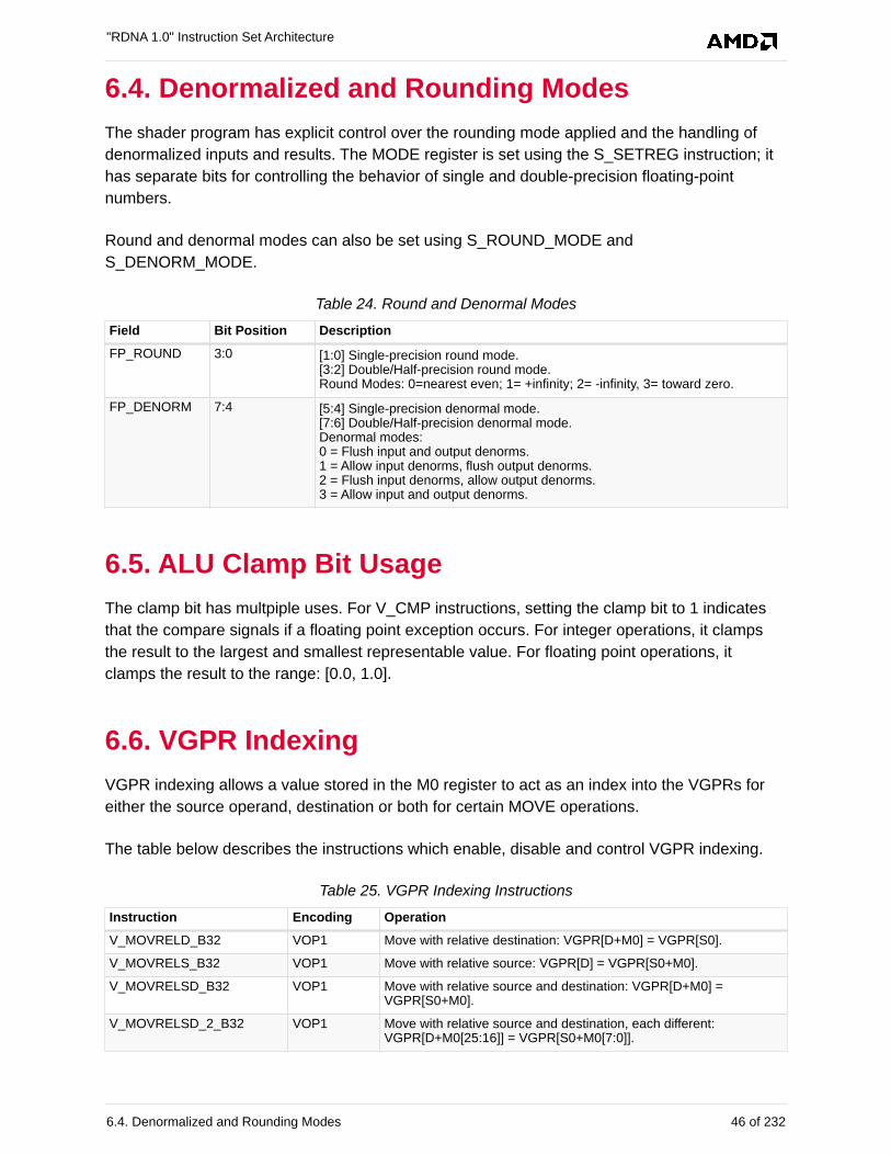
6.4. Denormalized and Rounding Modes
The shader program has explicit control over the rounding mode applied and the handling of
denormalized inputs and results. The MODE register is set using the S_SETREG instruction; it
has separate bits for controlling the behavior of single and double-precision floating-point
numbers.
Round and denormal modes can also be set using S_ROUND_MODE and
S_DENORM_MODE.
Table 24. Round and Denormal Modes
Field Bit Position Description
FP_ROUND 3:0 [1:0] Single-precision round mode.[3:2] Double/Half-precision round mode.Round Modes: 0=nearest even; 1= +infinity; 2= -infinity, 3= toward zero.
FP_DENORM 7:4 [5:4] Single-precision denormal mode.[7:6] Double/Half-precision denormal mode.Denormal modes:0 = Flush input and output denorms.1 = Allow input denorms, flush output denorms.2 = Flush input denorms, allow output denorms.3 = Allow input and output denorms.
6.5. ALU Clamp Bit Usage
The clamp bit has multpiple uses. For V_CMP instructions, setting the clamp bit to 1 indicates
that the compare signals if a floating point exception occurs. For integer operations, it clamps
the result to the largest and smallest representable value. For floating point operations, it
clamps the result to the range: [0.0, 1.0].
6.6. VGPR Indexing
VGPR indexing allows a value stored in the M0 register to act as an index into the VGPRs for
either the source operand, destination or both for certain MOVE operations.
The table below describes the instructions which enable, disable and control VGPR indexing.
Table 25. VGPR Indexing Instructions
Instruction Encoding Operation
V_MOVRELD_B32 VOP1 Move with relative destination: VGPR[D+M0] = VGPR[S0].
V_MOVRELS_B32 VOP1 Move with relative source: VGPR[D] = VGPR[S0+M0].
V_MOVRELSD_B32 VOP1 Move with relative source and destination: VGPR[D+M0] =VGPR[S0+M0].
V_MOVRELSD_2_B32 VOP1 Move with relative source and destination, each different:VGPR[D+M0[25:16]] = VGPR[S0+M0[7:0]].
"RDNA 1.0" Instruction Set Architecture
6.4. Denormalized and Rounding Modes 46 of 232
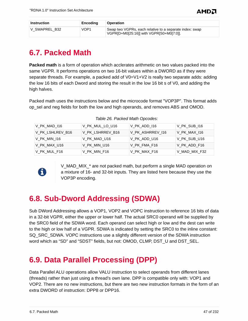
Instruction Encoding Operation
V_SWAPREL_B32 VOP1 Swap two VGPRs, each relative to a separate index: swapVGPR[D+M0[25:16]] with VGPR[S0+M0[7:0]].
6.7. Packed Math
Packed math is a form of operation which acclerates arithmetic on two values packed into the
same VGPR. It performs operations on two 16-bit values within a DWORD as if they were
separate threads. For example, a packed add of V0=V1+V2 is really two separate adds: adding
the low 16 bits of each Dword and storing the result in the low 16 bit s of V0, and adding the
high halves.
Packed math uses the instructions below and the microcode format "VOP3P". This format adds
op_sel and neg fields for both the low and high operands, and removes ABS and OMOD.
Table 26. Packed Math Opcodes:
V_PK_MAD_I16 V_PK_MUL_LO_U16 V_PK_ADD_I16 V_PK_SUB_I16
V_PK_LSHLREV_B16 V_PK_LSHRREV_B16 V_PK_ASHRREV_I16 V_PK_MAX_I16
V_PK_MIN_I16 V_PK_MAD_U16 V_PK_ADD_U16 V_PK_SUB_U16
V_PK_MAX_U16 V_PK_MIN_U16 V_PK_FMA_F16 V_PK_ADD_F16
V_PK_MUL_F16 V_PK_MIN_F16 V_PK_MAX_F16 V_MAD_MIX_F32
V_MAD_MIX_* are not packed math, but perform a single MAD operation on
a mixture of 16- and 32-bit inputs. They are listed here because they use the
VOP3P encoding.
6.8. Sub-Dword Addressing (SDWA)
Sub DWord Addressing allows a VOP1, VOP2 and VOPC instruction to reference 16 bits of data
in a 32-bit VGPR, either the upper or lower half. The actual SRC0 operand will be supplied by
the SRC0 field of the SDWA word. Each operand can select high or low and the dest can write
to the high or low half of a VGPR. SDWA is indicated by setting the SRC0 to the inline constant:
SQ_SRC_SDWA. VOPC instructions use a slightly different version of the SDWA instruction
word which as “SD” and “SDST” fields, but not: OMOD, CLMP, DST_U and DST_SEL.
6.9. Data Parallel Processing (DPP)
Data Parallel ALU operations allow VALU instruction to select operands from different lanes
(threads) rather than just using a thread’s own lane. DPP is compatible only with: VOP1 and
VOP2. There are no new instructions, but there are two new instruction formats in the form of an
extra DWORD of instruction: DPP8 or DPP16.
"RDNA 1.0" Instruction Set Architecture
6.7. Packed Math 47 of 232

There are two forms of the DPP instruction word:
DPP8
allows arbitrary swizzling between groups of 8 lanes
DPP16
allows a set of predefined swizzles between groups of 16 lanes
A scan operation is one which computes a value per thread which is based on the values of the
previous threads and possibly itself. E.g. a running sum is the sum of the values from previous
threads in the vector. A reduction operation is essentially a scan which returns a single value
from the highest numbered active thread. These operations take the SP multiple instruction
cycles (at least 8 times what an ADD_F32 takes). Rather than make these a single macro in
SQ, the shader program will have unique instructions for each pass of the scan. This prevents
any instruction scheduling issues (any other waves may execute in between these individual
stage instruction) and allows more general flexibility.
Use of DPP is indicated by setting the SRC0 operand to a literal constant: DPP8 or DPP16.
Note that since SRC-0 is set to the literal value, the actual VGPR address for Source-0 comes
from the literal constant (DPP). The scan operation requires the EXEC mask to be set to all 1’s
for proper operation. Unused threads (lanes) must be set to a value which will not change the
result prior to the scan. Readlane, readfirstlane and writelane cannot be used with DPP.
6.10. PERMLANE Specific Rules
V_PERMLANE must not occur immediately after a V_CMPX. To prevent this, any other VALU
opcode may be inserted (e.g. v_mov_b32 v0, v0).
"RDNA 1.0" Instruction Set Architecture
6.10. PERMLANE Specific Rules 48 of 232
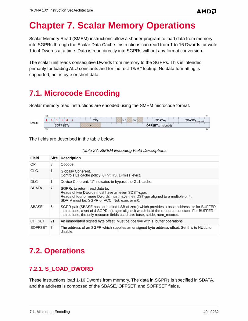
Chapter 7. Scalar Memory Operations
Scalar Memory Read (SMEM) instructions allow a shader program to load data from memory
into SGPRs through the Scalar Data Cache. Instructions can read from 1 to 16 Dwords, or write
1 to 4 Dwords at a time. Data is read directly into SGPRs without any format conversion.
The scalar unit reads consecutive Dwords from memory to the SGPRs. This is intended
primarily for loading ALU constants and for indirect T#/S# lookup. No data formatting is
supported, nor is byte or short data.
7.1. Microcode Encoding
Scalar memory read instructions are encoded using the SMEM microcode format.
The fields are described in the table below:
Table 27. SMEM Encoding Field Descriptions
Field Size Description
OP 8 Opcode.
GLC 1 Globally Coherent.Controls L1 cache policy: 0=hit_lru, 1=miss_evict.
DLC 1 Device Coherent. "1" indicates to bypass the GL1 cache.
SDATA 7 SGPRs to return read data to.Reads of two Dwords must have an even SDST-sgpr.Reads of four or more Dwords must have their DST-gpr aligned to a multiple of 4.SDATA must be: SGPR or VCC. Not: exec or m0.
SBASE 6 SGPR-pair (SBASE has an implied LSB of zero) which provides a base address, or for BUFFERinstructions, a set of 4 SGPRs (4-sgpr aligned) which hold the resource constant. For BUFFERinstructions, the only resource fields used are: base, stride, num_records.
OFFSET 21 An immediated signed byte offset. Must be positive with s_buffer operations.
SOFFSET 7 The address of an SGPR which supplies an unsigned byte address offset. Set this to NULL todisable.
7.2. Operations
7.2.1. S_LOAD_DWORD
These instructions load 1-16 Dwords from memory. The data in SGPRs is specified in SDATA,
and the address is composed of the SBASE, OFFSET, and SOFFSET fields.
"RDNA 1.0" Instruction Set Architecture
7.1. Microcode Encoding 49 of 232
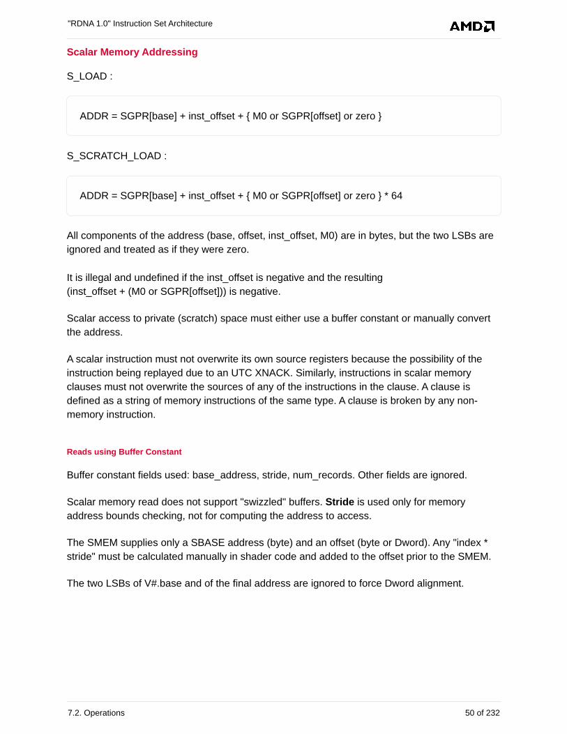
Scalar Memory Addressing
S_LOAD :
ADDR = SGPR[base] + inst_offset + { M0 or SGPR[offset] or zero }
S_SCRATCH_LOAD :
ADDR = SGPR[base] + inst_offset + { M0 or SGPR[offset] or zero } * 64
All components of the address (base, offset, inst_offset, M0) are in bytes, but the two LSBs are
ignored and treated as if they were zero.
It is illegal and undefined if the inst_offset is negative and the resulting
(inst_offset + (M0 or SGPR[offset])) is negative.
Scalar access to private (scratch) space must either use a buffer constant or manually convert
the address.
A scalar instruction must not overwrite its own source registers because the possibility of the
instruction being replayed due to an UTC XNACK. Similarly, instructions in scalar memory
clauses must not overwrite the sources of any of the instructions in the clause. A clause is
defined as a string of memory instructions of the same type. A clause is broken by any non-
memory instruction.
Reads using Buffer Constant
Buffer constant fields used: base_address, stride, num_records. Other fields are ignored.
Scalar memory read does not support "swizzled" buffers. Stride is used only for memory
address bounds checking, not for computing the address to access.
The SMEM supplies only a SBASE address (byte) and an offset (byte or Dword). Any "index *
stride" must be calculated manually in shader code and added to the offset prior to the SMEM.
The two LSBs of V#.base and of the final address are ignored to force Dword alignment.
"RDNA 1.0" Instruction Set Architecture
7.2. Operations 50 of 232
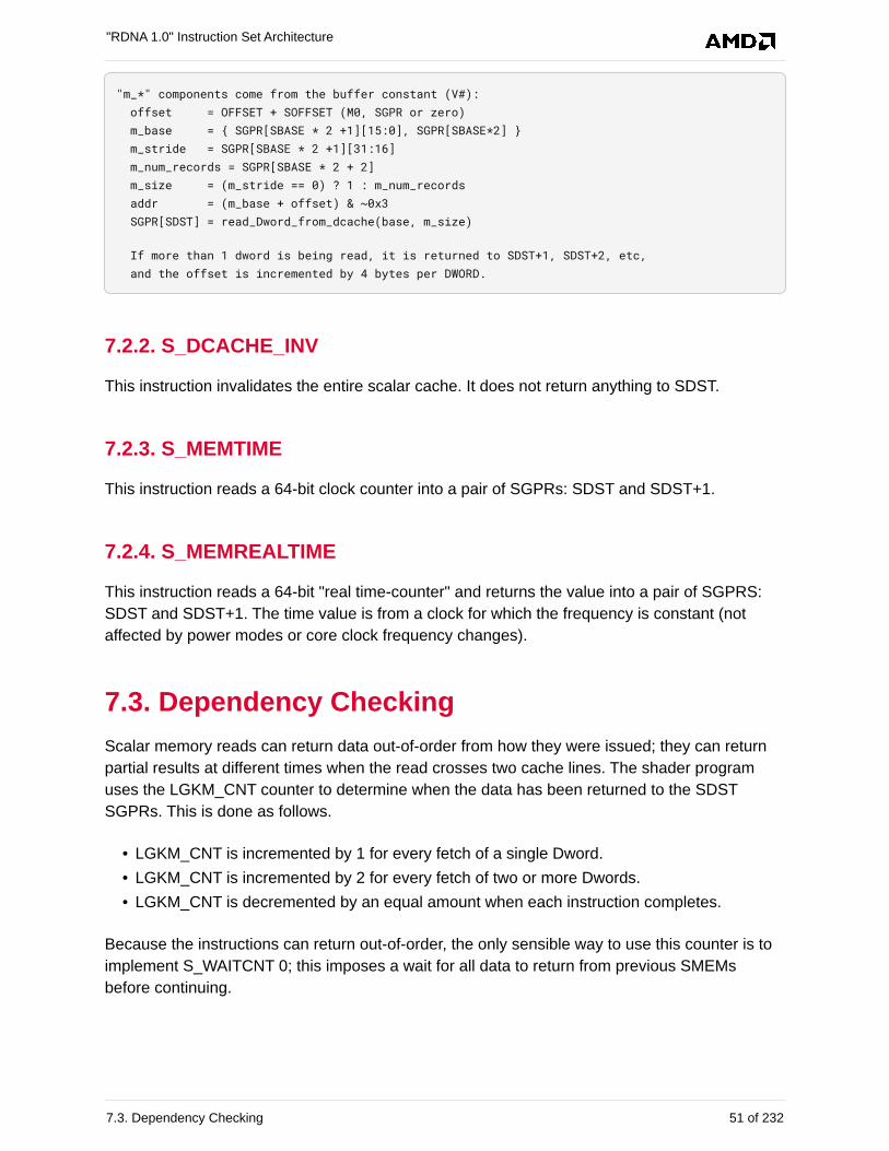
"m_*" components come from the buffer constant (V#): offset = OFFSET + SOFFSET (M0, SGPR or zero) m_base = { SGPR[SBASE * 2 +1][15:0], SGPR[SBASE*2] } m_stride = SGPR[SBASE * 2 +1][31:16] m_num_records = SGPR[SBASE * 2 + 2] m_size = (m_stride == 0) ? 1 : m_num_records addr = (m_base + offset) & ~0x3 SGPR[SDST] = read_Dword_from_dcache(base, m_size)
If more than 1 dword is being read, it is returned to SDST+1, SDST+2, etc, and the offset is incremented by 4 bytes per DWORD.
7.2.2. S_DCACHE_INV
This instruction invalidates the entire scalar cache. It does not return anything to SDST.
7.2.3. S_MEMTIME
This instruction reads a 64-bit clock counter into a pair of SGPRs: SDST and SDST+1.
7.2.4. S_MEMREALTIME
This instruction reads a 64-bit "real time-counter" and returns the value into a pair of SGPRS:
SDST and SDST+1. The time value is from a clock for which the frequency is constant (not
affected by power modes or core clock frequency changes).
7.3. Dependency Checking
Scalar memory reads can return data out-of-order from how they were issued; they can return
partial results at different times when the read crosses two cache lines. The shader program
uses the LGKM_CNT counter to determine when the data has been returned to the SDST
SGPRs. This is done as follows.
• LGKM_CNT is incremented by 1 for every fetch of a single Dword.
• LGKM_CNT is incremented by 2 for every fetch of two or more Dwords.
• LGKM_CNT is decremented by an equal amount when each instruction completes.
Because the instructions can return out-of-order, the only sensible way to use this counter is to
implement S_WAITCNT 0; this imposes a wait for all data to return from previous SMEMs
before continuing.
"RDNA 1.0" Instruction Set Architecture
7.3. Dependency Checking 51 of 232
7.4. Scalar Memory Clauses and Groups
A “clause” is a sequence of instructions starting with S_CLAUSE and continuing for 2-63
instructions. Clauses lock the instruction arbiter onto this wave until the clause completes.
A “group” is a set of the same type of instruction that happen to occur in the code but are not
necessarily executed as a clause. A group ends when there a non-SMEM instruction.
Scalar memory instructions are issued in groups. A group is a sequence of SMEM instructions,
and any non-SMEM instruction breaks the group. The hardware does not enforce that a single
wave will execute an entire group before issuing instructions from another wave.
Group restrictions:
1. Reads and writes must not be in the same group if they might access the same addresses
2. INV must be in a group by itself
3. “TIME” instructions are considered as reads for group rules
Instruction ordering
The data cache is free to re-order instructions. The only assurance of ordering comes when the
shader executes an S_WAITCNT LGKMcnt==0. Cache invalidate instructions are not assured to
have completed until the shader waits for LGKMcnt==0.
7.5. Alignment and Bounds Checking
SDST
The value of SDST must be even for fetches of two Dwords (including S_MEMTIME), or a
multiple of four for larger fetches. If this rule is not followed, invalid data can result. If SDST
is out-of-range, the instruction is not executed.
SBASE
The value of SBASE must be even for S_BUFFER_LOAD (specifying the address of an
SGPR which is a multiple of four). If SBASE is out-of-range, the value from SGPR0 is used.
OFFSET
The value of OFFSET has no alignment restrictions.
Memory Address : If the memory address is out-of-range (clamped), the operation is not
performed for any Dwords that are out-of-range.
"RDNA 1.0" Instruction Set Architecture
7.4. Scalar Memory Clauses and Groups 52 of 232
Chapter 8. Vector Memory Operations
Vector Memory (VMEM) instructions read or write one piece of data separately for each work-
item in a wavefront into, or out of, VGPRs. This is in contrast to Scalar Memory instructions,
which move a single piece of data that is shared by all threads in the wavefront. All Vector
Memory (VM) operations are processed by the texture cache system (level 1 and level 2
caches).
Software initiates a load, store or atomic operation through the texture cache through one of
three types of VMEM instructions:
• MTBUF: Memory typed-buffer operations.
• MUBUF: Memory untyped-buffer operations.
• MIMG: Memory image operations.
The instruction defines which VGPR(s) supply the addresses for the operation, which VGPRs
supply or receive data from the operation, and a series of SGPRs that contain the memory
buffer descriptor (V# or T#). Also, MIMG operations supply a texture sampler (S#) from a series
of four SGPRs; this sampler defines texel filtering operations to be performed on data read from
the image.
8.1. Vector Memory Buffer Instructions
Vector-memory (VM) operations transfer data between the VGPRs and buffer objects in memory
through the texture cache (TC). Vector means that one or more piece of data is transferred
uniquely for every thread in the wavefront, in contrast to scalar memory reads, which transfer
only one value that is shared by all threads in the wavefront.
Buffer reads have the option of returning data to VGPRs or directly into LDS.
Examples of buffer objects are vertex buffers, raw buffers, stream-out buffers, and structured
buffers.
Buffer objects support both homogeneous and heterogeneous data, but no filtering of read-data
(no samplers). Buffer instructions are divided into two groups:
• MUBUF: Untyped buffer objects.
◦ Data format is specified in the resource constant.
◦ Load, store, atomic operations, with or without data format conversion.
• MTBUF: Typed buffer objects.
◦ Data format is specified in the instruction.
◦ The only operations are Load and Store, both with data format conversion.
Atomic operations take data from VGPRs and combine them arithmetically with data already in
"RDNA 1.0" Instruction Set Architecture
8.1. Vector Memory Buffer Instructions 53 of 232
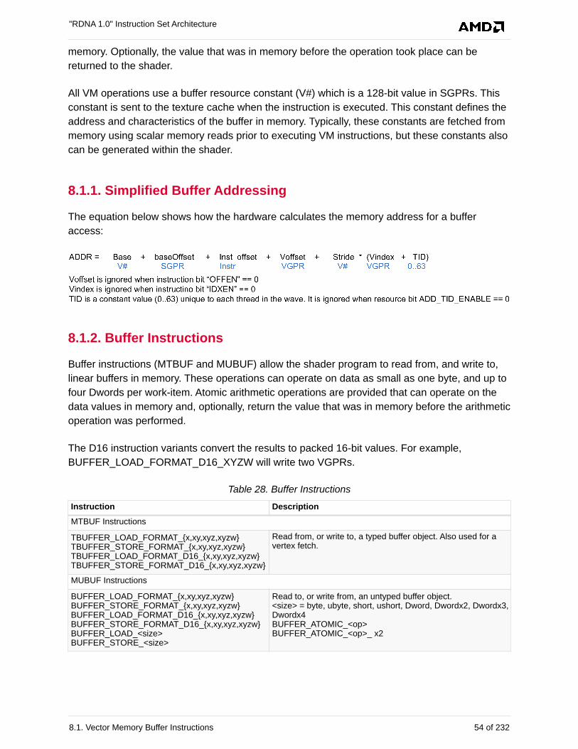
memory. Optionally, the value that was in memory before the operation took place can be
returned to the shader.
All VM operations use a buffer resource constant (V#) which is a 128-bit value in SGPRs. This
constant is sent to the texture cache when the instruction is executed. This constant defines the
address and characteristics of the buffer in memory. Typically, these constants are fetched from
memory using scalar memory reads prior to executing VM instructions, but these constants also
can be generated within the shader.
8.1.1. Simplified Buffer Addressing
The equation below shows how the hardware calculates the memory address for a buffer
access:
8.1.2. Buffer Instructions
Buffer instructions (MTBUF and MUBUF) allow the shader program to read from, and write to,
linear buffers in memory. These operations can operate on data as small as one byte, and up to
four Dwords per work-item. Atomic arithmetic operations are provided that can operate on the
data values in memory and, optionally, return the value that was in memory before the arithmetic
operation was performed.
The D16 instruction variants convert the results to packed 16-bit values. For example,
BUFFER_LOAD_FORMAT_D16_XYZW will write two VGPRs.
Table 28. Buffer Instructions
Instruction Description
MTBUF Instructions
TBUFFER_LOAD_FORMAT_{x,xy,xyz,xyzw}TBUFFER_STORE_FORMAT_{x,xy,xyz,xyzw}TBUFFER_LOAD_FORMAT_D16_{x,xy,xyz,xyzw}TBUFFER_STORE_FORMAT_D16_{x,xy,xyz,xyzw}
Read from, or write to, a typed buffer object. Also used for avertex fetch.
MUBUF Instructions
BUFFER_LOAD_FORMAT_{x,xy,xyz,xyzw}BUFFER_STORE_FORMAT_{x,xy,xyz,xyzw}BUFFER_LOAD_FORMAT_D16_{x,xy,xyz,xyzw}BUFFER_STORE_FORMAT_D16_{x,xy,xyz,xyzw}BUFFER_LOAD_<size>BUFFER_STORE_<size>
Read to, or write from, an untyped buffer object.<size> = byte, ubyte, short, ushort, Dword, Dwordx2, Dwordx3,Dwordx4BUFFER_ATOMIC_<op>BUFFER_ATOMIC_<op>_ x2
"RDNA 1.0" Instruction Set Architecture
8.1. Vector Memory Buffer Instructions 54 of 232
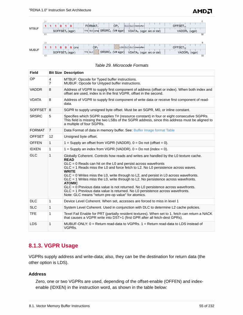
Table 29. Microcode Formats
Field Bit Size Description
OP 47
MTBUF: Opcode for Typed buffer instructions.MUBUF: Opcode for Untyped buffer instructions.
VADDR 8 Address of VGPR to supply first component of address (offset or index). When both index andoffset are used, index is in the first VGPR, offset in the second.
VDATA 8 Address of VGPR to supply first component of write data or receive first component of read-data.
SOFFSET 8 SGPR to supply unsigned byte offset. Must be an SGPR, M0, or inline constant.
SRSRC 5 Specifies which SGPR supplies T# (resource constant) in four or eight consecutive SGPRs.This field is missing the two LSBs of the SGPR address, since this address must be aligned toa multiple of four SGPRs.
FORMAT 7 Data Format of data in memory buffer. See: Buffer Image format Table
OFFSET 12 Unsigned byte offset.
OFFEN 1 1 = Supply an offset from VGPR (VADDR). 0 = Do not (offset = 0).
IDXEN 1 1 = Supply an index from VGPR (VADDR). 0 = Do not (index = 0).
GLC 1 Globally Coherent. Controls how reads and writes are handled by the L0 texture cache.READGLC = 0 Reads can hit on the L0 and persist across wavefrontsGLC = 1 Reads miss the L0 and force fetch to L2. No L0 persistence across waves.WRITEGLC = 0 Writes miss the L0, write through to L2, and persist in L0 across wavefronts.GLC = 1 Writes miss the L0, write through to L2. No persistence across wavefronts.ATOMICGLC = 0 Previous data value is not returned. No L0 persistence across wavefronts.GLC = 1 Previous data value is returned. No L0 persistence across wavefronts.Note: GLC means "return pre-op value" for atomics.
DLC 1 Device Level Coherent. When set, accesses are forced to miss in level 1
SLC 1 System Level Coherent. Used in conjunction with DLC to determine L2 cache policies.
TFE 1 Texel Fail Enable for PRT (partially resident textures). When set to 1, fetch can return a NACKthat causes a VGPR write into DST+1 (first GPR after all fetch-dest GPRs).
LDS 1 MUBUF-ONLY: 0 = Return read-data to VGPRs. 1 = Return read-data to LDS instead ofVGPRs.
8.1.3. VGPR Usage
VGPRs supply address and write-data; also, they can be the destination for return data (the
other option is LDS).
Address
Zero, one or two VGPRs are used, depending of the offset-enable (OFFEN) and index-
enable (IDXEN) in the instruction word, as shown in the table below:
"RDNA 1.0" Instruction Set Architecture
8.1. Vector Memory Buffer Instructions 55 of 232
Table 30. Address VGPRs
IDXEN OFFEN VGPRn VGPRn+1
0 0 nothing
0 1 uint offset
1 0 uint index
1 1 uint index uint offset
Write Data : N consecutive VGPRs, starting at VDATA. The data format specified in the
instruction word (FORMAT for MTBUF, or encoded in the opcode field for MUBUF) determines
how many Dwords to write.
Read Data : Same as writes. Data is returned to consecutive GPRs.
Read Data Format : Read data is 32 bits, based on the data format in the instruction or
resource. Float or normalized data is returned as floats; integer formats are returned as integers
(signed or unsigned, same type as the memory storage format). Memory reads of data in
memory that is 32 or 64 bits do not undergo any format conversion.
Atomics with Return : Data is read out of the VGPR(s) starting at VDATA to supply to the
atomic operation. If the atomic returns a value to VGPRs, that data is returned to those same
VGPRs starting at VDATA.
8.1.4. Buffer Data
The amount and type of data that is read or written is controlled by the following: the resource
format field, destination-component-selects (dst_sel), and the opcode. FORMAT can come from
the resource, instruction fields, or the opcode itself. Dst_sel comes from the resource, but is
ignored for many operations.
Table 31. Buffer Instructions
Instruction Data Format Num Format DST SEL
TBUFFER_LOAD_FORMAT_* instruction instruction identity
TBUFFER_STORE_FORMAT_* instruction instruction identity
BUFFER_LOAD_<type> derived derived identity
BUFFER_STORE_<type> derived derived identity
BUFFER_LOAD_FORMAT_* resource resource resource
BUFFER_STORE_FORMAT_* resource resource resource
BUFFER_ATOMIC_* derived derived identity
Instruction : The instruction’s format field is used instead of the resource’s fields.
Data format derived : The data format is derived from the opcode and ignores the resource
definition. For example, buffer_load_ubyte sets the data-format to 8 and number-format to uint.
"RDNA 1.0" Instruction Set Architecture
8.1. Vector Memory Buffer Instructions 56 of 232
The resource’s data format must not be INVALID; that format has specific
meaning (unbound resource), and for that case the data format is not
replaced by the instruction’s implied data format.
DST_SEL identity : Depending on the number of components in the data-format, this is: X000,
XY00, XYZ0, or XYZW.
The MTBUF derives the data format from the instruction. The MUBUF
BUFFER_LOAD_FORMAT and BUFFER_STORE_FORMAT instructions use dst_sel from the
resource; other MUBUF instructions derive data-format from the instruction itself.
D16 Instructions : Load-format and store-format instructions also come in a "d16" variant. For
stores, each 32-bit VGPR holds two 16-bit data elements that are passed to the texture unit.
This texture unit converts them to the texture format before writing to memory. For loads, data
returned from the texture unit is converted to 16 bits, and a pair of data are stored in each 32-bit
VGPR (LSBs first, then MSBs). Control over int vs. float is controlled by FORMAT.
8.1.5. Buffer Addressing
A buffer is a data structure in memory that is addressed with an index and an offset. The index
points to a particular record of size stride bytes, and the offset is the byte-offset within the
record. The stride comes from the resource, the index from a VGPR (or zero), and the offset
from an SGPR or VGPR and also from the instruction itself.
Table 32. BUFFER Instruction Fields for Addressing
Field Size Description
inst_offset 12 Literal byte offset from the instruction.
inst_idxen 1 Boolean: get index from VGPR when true, or no index when false.
inst_offen 1 Boolean: get offset from VGPR when true, or no offset when false. Note that inst_offset ispresent, regardless of this bit.
The "element size" for a buffer instruction is the amount of data the instruction transfers. It is the
number of contiguous bytes of a record for a given index, and is fixed at 4 bytes.
Table 33. V# Buffer Resource Constant Fields for Addressing
Field Size Description
const_base 48 Base address, in bytes, of the buffer resource.
const_stride 14 Stride of the record in bytes (0 to 16,383 bytes, or 0 to
262,143 bytes).
"RDNA 1.0" Instruction Set Architecture
8.1. Vector Memory Buffer Instructions 57 of 232
Field Size Description
const_num_records 32Number of records in the buffer.
In units of:
Bytes if: const_stride == 0 || or const_swizzle_enable == false
Otherwise, in units of "stride".
const_add_tid_enable 1 Boolean. Add thread_ID within the wavefront to the index
when true.
const_swizzle_enable 1 Boolean. Indicates that the surface is swizzled when true.
const_index_stride 2 Used only when const_swizzle_en = true. Number of
contiguous indices for a single element (of element_size)
before switching to the next element. There are 8, 16, 32, or
64 indices.
Table 34. Address Components from GPRs
Field Size Description
SGPR_offset 32 An unsigned byte-offset to the address. Comes from an SGPR or M0.
VGPR_offset 32 An optional unsigned byte-offset. It is per-thread, and comes from a VGPR.
VGPR_index 32 An optional index value. It is per-thread and comes from a VGPR.
The final buffer memory address is composed of three parts:
• the base address from the buffer resource (V#),
• the offset from the SGPR, and
• a buffer-offset that is calculated differently, depending on whether the buffer is linearly
addressed (a simple Array-of-Structures calculation) or is swizzled.
"RDNA 1.0" Instruction Set Architecture
8.1. Vector Memory Buffer Instructions 58 of 232
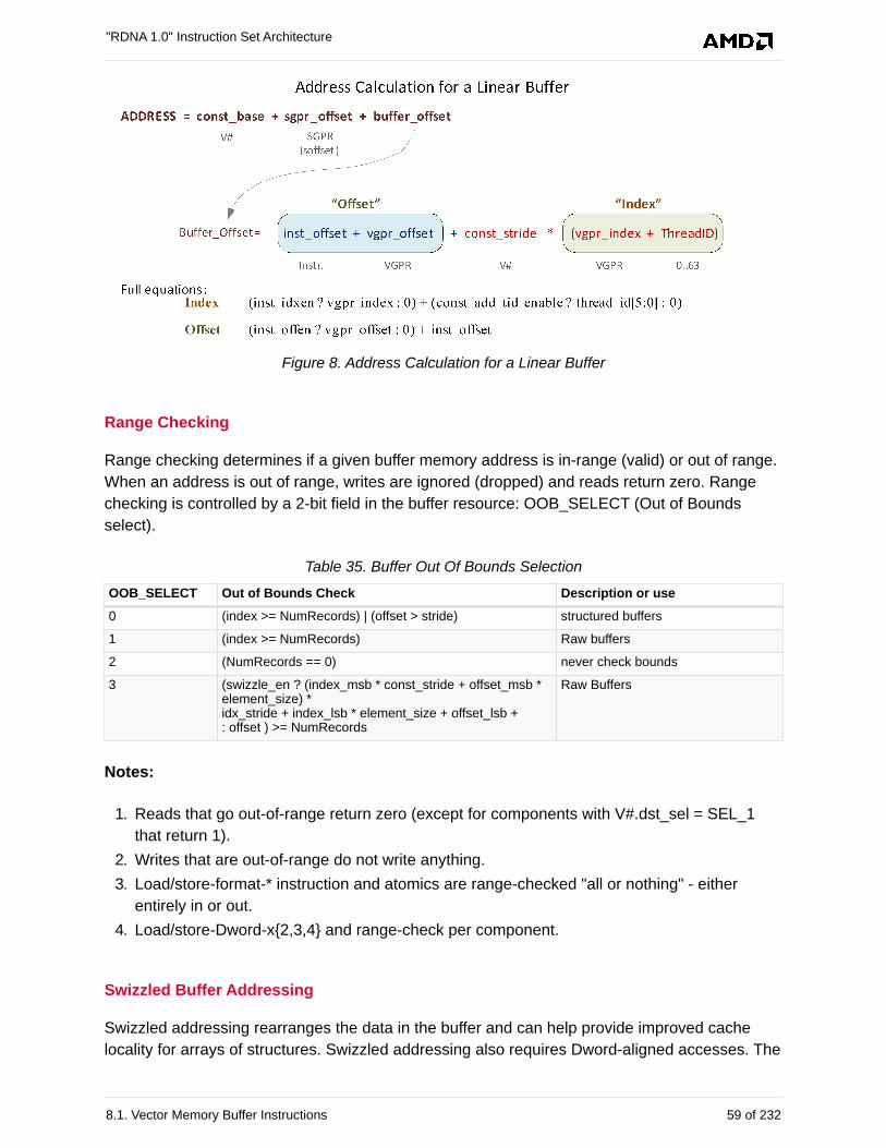
Figure 8. Address Calculation for a Linear Buffer
Range Checking
Range checking determines if a given buffer memory address is in-range (valid) or out of range.
When an address is out of range, writes are ignored (dropped) and reads return zero. Range
checking is controlled by a 2-bit field in the buffer resource: OOB_SELECT (Out of Bounds
select).
Table 35. Buffer Out Of Bounds Selection
OOB_SELECT Out of Bounds Check Description or use
0 (index >= NumRecords) | (offset > stride) structured buffers
1 (index >= NumRecords) Raw buffers
2 (NumRecords == 0) never check bounds
3 (swizzle_en ? (index_msb * const_stride + offset_msb *element_size) *idx_stride + index_lsb * element_size + offset_lsb +: offset ) >= NumRecords
Raw Buffers
Notes:
1. Reads that go out-of-range return zero (except for components with V#.dst_sel = SEL_1
that return 1).
2. Writes that are out-of-range do not write anything.
3. Load/store-format-* instruction and atomics are range-checked "all or nothing" - either
entirely in or out.
4. Load/store-Dword-x{2,3,4} and range-check per component.
Swizzled Buffer Addressing
Swizzled addressing rearranges the data in the buffer and can help provide improved cache
locality for arrays of structures. Swizzled addressing also requires Dword-aligned accesses. The
"RDNA 1.0" Instruction Set Architecture
8.1. Vector Memory Buffer Instructions 59 of 232
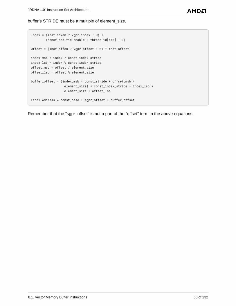
buffer’s STRIDE must be a multiple of element_size.
Index = (inst_idxen ? vgpr_index : 0) + (const_add_tid_enable ? thread_id[5:0] : 0)
Offset = (inst_offen ? vgpr_offset : 0) + inst_offset
index_msb = index / const_index_strideindex_lsb = index % const_index_strideoffset_msb = offset / element_sizeoffset_lsb = offset % element_size
buffer_offset = (index_msb * const_stride + offset_msb * element_size) * const_index_stride + index_lsb * element_size + offset_lsb
Final Address = const_base + sgpr_offset + buffer_offset
Remember that the "sgpr_offset" is not a part of the "offset" term in the above equations.
"RDNA 1.0" Instruction Set Architecture
8.1. Vector Memory Buffer Instructions 60 of 232
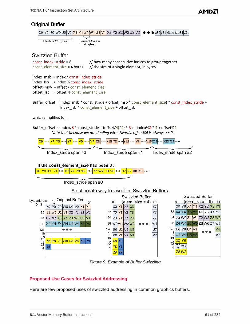
Figure 9. Example of Buffer Swizzling
Proposed Use Cases for Swizzled Addressing
Here are few proposed uses of swizzled addressing in common graphics buffers.
"RDNA 1.0" Instruction Set Architecture
8.1. Vector Memory Buffer Instructions 61 of 232
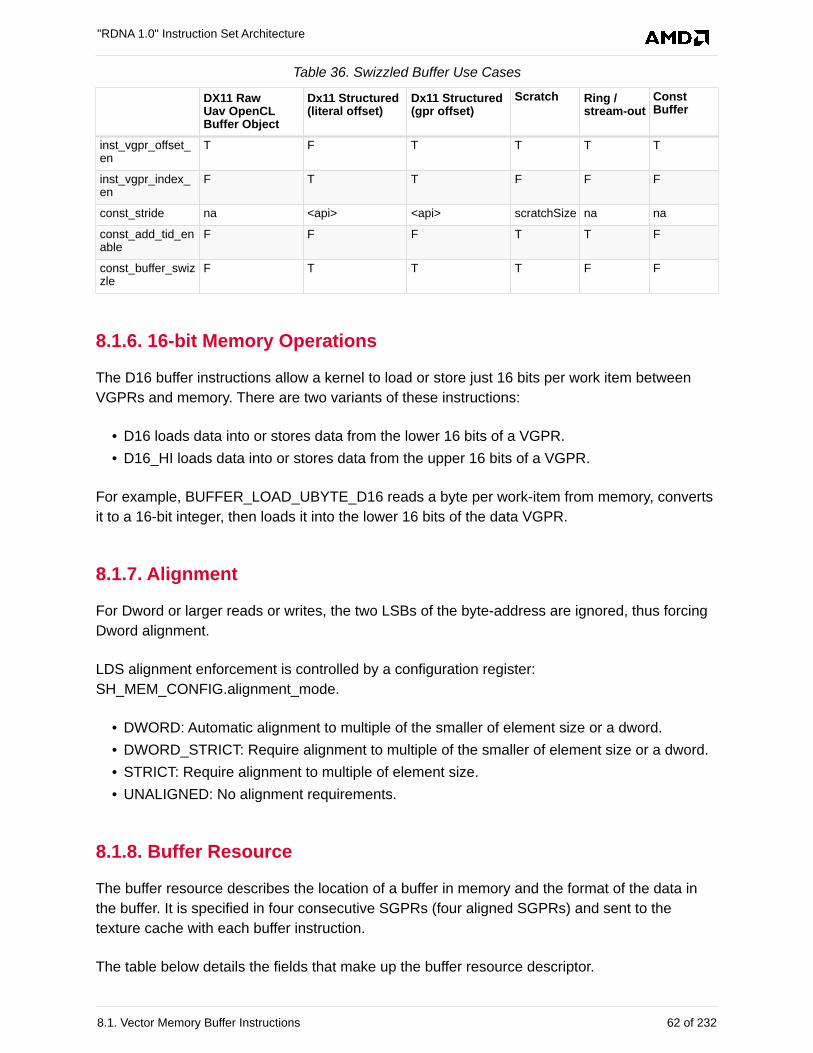
Table 36. Swizzled Buffer Use Cases
DX11 RawUav OpenCLBuffer Object
Dx11 Structured(literal offset)
Dx11 Structured(gpr offset)
Scratch Ring /stream-out
ConstBuffer
inst_vgpr_offset_en
T F T T T T
inst_vgpr_index_en
F T T F F F
const_stride na <api> <api> scratchSize na na
const_add_tid_enable
F F F T T F
const_buffer_swizzle
F T T T F F
8.1.6. 16-bit Memory Operations
The D16 buffer instructions allow a kernel to load or store just 16 bits per work item between
VGPRs and memory. There are two variants of these instructions:
• D16 loads data into or stores data from the lower 16 bits of a VGPR.
• D16_HI loads data into or stores data from the upper 16 bits of a VGPR.
For example, BUFFER_LOAD_UBYTE_D16 reads a byte per work-item from memory, converts
it to a 16-bit integer, then loads it into the lower 16 bits of the data VGPR.
8.1.7. Alignment
For Dword or larger reads or writes, the two LSBs of the byte-address are ignored, thus forcing
Dword alignment.
LDS alignment enforcement is controlled by a configuration register:
SH_MEM_CONFIG.alignment_mode.
• DWORD: Automatic alignment to multiple of the smaller of element size or a dword.
• DWORD_STRICT: Require alignment to multiple of the smaller of element size or a dword.
• STRICT: Require alignment to multiple of element size.
• UNALIGNED: No alignment requirements.
8.1.8. Buffer Resource
The buffer resource describes the location of a buffer in memory and the format of the data in
the buffer. It is specified in four consecutive SGPRs (four aligned SGPRs) and sent to the
texture cache with each buffer instruction.
The table below details the fields that make up the buffer resource descriptor.
"RDNA 1.0" Instruction Set Architecture
8.1. Vector Memory Buffer Instructions 62 of 232
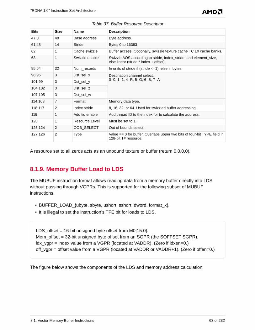
Table 37. Buffer Resource Descriptor
Bits Size Name Description
47:0 48 Base address Byte address.
61:48 14 Stride Bytes 0 to 16383
62 1 Cache swizzle Buffer access. Optionally, swizzle texture cache TC L0 cache banks.
63 1 Swizzle enable Swizzle AOS according to stride, index_stride, and element_size,else linear (stride * index + offset).
95:64 32 Num_records In units of stride if (stride <=1), else in bytes.
98:96 3 Dst_sel_x Destination channel select:0=0, 1=1, 4=R, 5=G, 6=B, 7=A
101:99 3 Dst_sel_y
104:102 3 Dst_sel_z
107:105 3 Dst_sel_w
114:108 7 Format Memory data type.
118:117 2 Index stride 8, 16, 32, or 64. Used for swizzled buffer addressing.
119 1 Add tid enable Add thread ID to the index for to calculate the address.
120 1 Resource Level Must be set to 1.
125:124 2 OOB_SELECT Out of bounds select.
127:126 2 Type Value == 0 for buffer. Overlaps upper two bits of four-bit TYPE field in128-bit T# resource.
A resource set to all zeros acts as an unbound texture or buffer (return 0,0,0,0).
8.1.9. Memory Buffer Load to LDS
The MUBUF instruction format allows reading data from a memory buffer directly into LDS
without passing through VGPRs. This is supported for the following subset of MUBUF
instructions.
• BUFFER_LOAD_{ubyte, sbyte, ushort, sshort, dword, format_x}.
• It is illegal to set the instruction’s TFE bit for loads to LDS.
LDS_offset = 16-bit unsigned byte offset from M0[15:0].
Mem_offset = 32-bit unsigned byte offset from an SGPR (the SOFFSET SGPR).
idx_vgpr = index value from a VGPR (located at VADDR). (Zero if idxen=0.)
off_vgpr = offset value from a VGPR (located at VADDR or VADDR+1). (Zero if offen=0.)
The figure below shows the components of the LDS and memory address calculation:
"RDNA 1.0" Instruction Set Architecture
8.1. Vector Memory Buffer Instructions 63 of 232
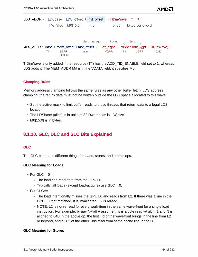
TIDinWave is only added if the resource (T#) has the ADD_TID_ENABLE field set to 1, whereas
LDS adds it. The MEM_ADDR M# is in the VDATA field; it specifies M0.
Clamping Rules
Memory address clamping follows the same rules as any other buffer fetch. LDS address
clamping: the return data must not be written outside the LDS space allocated to this wave.
• Set the active-mask to limit buffer reads to those threads that return data to a legal LDS
location.
• The LDSbase (alloc) is in units of 32 Dwords, as is LDSsize.
• M0[15:0] is in bytes.
8.1.10. GLC, DLC and SLC Bits Explained
GLC
The GLC bit means different things for loads, stores, and atomic ops.
GLC Meaning for Loads
• For GLC==0
◦ The load can read data from the GPU L0.
◦ Typically, all loads (except load-acquire) use GLC==0.
• For GLC==1
◦ The load intentionally misses the GPU L0 and reads from L2. If there was a line in the
GPU L0 that matched, it is invalidated; L2 is reread.
◦ NOTE: L2 is not re-read for every work-item in the same wave-front for a single load
instruction. For example: b=uav[N+tid] // assume this is a byte read w/ glc==1 and N is
aligned to 64B In the above op, the first Tid of the wavefront brings in the line from L2
or beyond, and all 63 of the other Tids read from same cache line in the L0.
GLC Meaning for Stores
"RDNA 1.0" Instruction Set Architecture
8.1. Vector Memory Buffer Instructions 64 of 232
• For GLC==0 This causes a write-combine across work-items of the wavefront store op;
dirtied lines are written to the L2 automatically.
◦ If the store operation dirtied all bytes of the 64 B line, it is left clean and valid in the L0;
subsequent accesses to the cache are allowed to hit on this cache line.
◦ Else do not leave write-combined lines in L0.
• For GLC==1 Same as GLC==0, except the write-combined lines are not left in the line,
even if all bytes are dirtied.
Atomics
• For GLC == 0 No return data (this is "write-only" atomic op).
• For GLC == 1 Returns previous value in memory (before the atomic operation).
DLC and SLC
The Device Level Coherent bit (DLC) and System Level Coherent (SLC) bits control the
behavior of the second and third level caches.
Table 38. Vector Load Operations
SLC DLC L2 Cache L1 Cache
0 0 LRU Hit LRU - reads can hit on previous data
0 1 LRU Miss Evict - reads miss
1 0 Stream Hit LRU
1 1 Hit No Allocate Miss Evict
Table 39. Vector Store & Atomic Operations
SLC DLC L2 Cache
0 0 LRU
0 1 Bypass
1 0 Stream - Hit leaves line in cache but do not reset age.
1 1 Hit No Allocate
For stores and atomics, the L1 cache is bypassed (but is coherent).
For stores the L0 cache is controlled by GLC: 0 = Miss-LRU (leave completely directly
cachelines valid in the cache), 1 = Miss-Evict.
8.2. Vector Memory (VM) Image Instructions
Vector Memory (VM) operations transfer data between the VGPRs and memory through the
texture cache (TC). Vector means the transfer of one or more pieces of data uniquely for every
work-item in the wavefront. This is in contrast to scalar memory reads, which transfer only one
value that is shared by all work-items in the wavefront.
"RDNA 1.0" Instruction Set Architecture
8.2. Vector Memory (VM) Image Instructions 65 of 232
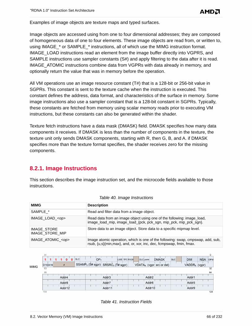
Examples of image objects are texture maps and typed surfaces.
Image objects are accessed using from one to four dimensional addresses; they are composed
of homogeneous data of one to four elements. These image objects are read from, or written to,
using IMAGE_* or SAMPLE_* instructions, all of which use the MIMG instruction format.
IMAGE_LOAD instructions read an element from the image buffer directly into VGPRS, and
SAMPLE instructions use sampler constants (S#) and apply filtering to the data after it is read.
IMAGE_ATOMIC instructions combine data from VGPRs with data already in memory, and
optionally return the value that was in memory before the operation.
All VM operations use an image resource constant (T#) that is a 128-bit or 256-bit value in
SGPRs. This constant is sent to the texture cache when the instruction is executed. This
constant defines the address, data format, and characteristics of the surface in memory. Some
image instructions also use a sampler constant that is a 128-bit constant in SGPRs. Typically,
these constants are fetched from memory using scalar memory reads prior to executing VM
instructions, but these constants can also be generated within the shader.
Texture fetch instructions have a data mask (DMASK) field. DMASK specifies how many data
components it receives. If DMASK is less than the number of components in the texture, the
texture unit only sends DMASK components, starting with R, then G, B, and A. if DMASK
specifies more than the texture format specifies, the shader receives zero for the missing
components.
8.2.1. Image Instructions
This section describes the image instruction set, and the microcode fields available to those
instructions.
Table 40. Image Instructions
MIMG Description
SAMPLE_* Read and filter data from a image object.
IMAGE_LOAD_<op> Read data from an image object using one of the following: image_load,image_load_mip, image_load_{pck, pck_sgn, mip_pck, mip_pck_sgn}.
IMAGE_STOREIMAGE_STORE_MIP
Store data to an image object. Store data to a specific mipmap level.
IMAGE_ATOMIC_<op> Image atomic operation, which is one of the following: swap, cmpswap, add, sub,rsub, {u,s}{min,max}, and, or, xor, inc, dec, fcmpswap, fmin, fmax.
Table 41. Instruction Fields
"RDNA 1.0" Instruction Set Architecture
8.2. Vector Memory (VM) Image Instructions 66 of 232
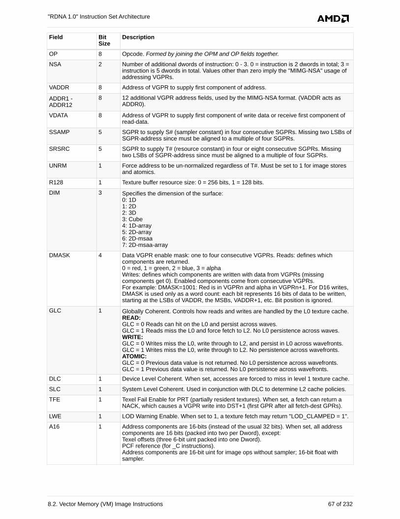
Field BitSize
Description
OP 8 Opcode. Formed by joining the OPM and OP fields together.
NSA 2 Number of additional dwords of instruction: 0 - 3. 0 = instruction is 2 dwords in total; 3 =instruction is 5 dwords in total. Values other than zero imply the "MIMG-NSA" usage ofaddressing VGPRs.
VADDR 8 Address of VGPR to supply first component of address.
ADDR1 -ADDR12
8 12 additional VGPR address fields, used by the MIMG-NSA format. (VADDR acts asADDR0).
VDATA 8 Address of VGPR to supply first component of write data or receive first component ofread-data.
SSAMP 5 SGPR to supply S# (sampler constant) in four consecutive SGPRs. Missing two LSBs ofSGPR-address since must be aligned to a multiple of four SGPRs.
SRSRC 5 SGPR to supply T# (resource constant) in four or eight consecutive SGPRs. Missingtwo LSBs of SGPR-address since must be aligned to a multiple of four SGPRs.
UNRM 1 Force address to be un-normalized regardless of T#. Must be set to 1 for image storesand atomics.
R128 1 Texture buffer resource size: 0 = 256 bits, 1 = 128 bits.
DIM 3 Specifies the dimension of the surface:0: 1D1: 2D2: 3D3: Cube4: 1D-array5: 2D-array6: 2D-msaa7: 2D-msaa-array
DMASK 4 Data VGPR enable mask: one to four consecutive VGPRs. Reads: defines whichcomponents are returned.0 = red, 1 = green, 2 = blue, 3 = alphaWrites: defines which components are written with data from VGPRs (missingcomponents get 0). Enabled components come from consecutive VGPRs.For example: DMASK=1001: Red is in VGPRn and alpha in VGPRn+1. For D16 writes,DMASK is used only as a word count: each bit represents 16 bits of data to be written,starting at the LSBs of VADDR, the MSBs, VADDR+1, etc. Bit position is ignored.
GLC 1 Globally Coherent. Controls how reads and writes are handled by the L0 texture cache.READ:GLC = 0 Reads can hit on the L0 and persist across waves.GLC = 1 Reads miss the L0 and force fetch to L2. No L0 persistence across waves.WRITE:GLC = 0 Writes miss the L0, write through to L2, and persist in L0 across wavefronts.GLC = 1 Writes miss the L0, write through to L2. No persistence across wavefronts.ATOMIC:GLC = 0 Previous data value is not returned. No L0 persistence across wavefronts.GLC = 1 Previous data value is returned. No L0 persistence across wavefronts.
DLC 1 Device Level Coherent. When set, accesses are forced to miss in level 1 texture cache.
SLC 1 System Level Coherent. Used in conjunction with DLC to determine L2 cache policies.
TFE 1 Texel Fail Enable for PRT (partially resident textures). When set, a fetch can return aNACK, which causes a VGPR write into DST+1 (first GPR after all fetch-dest GPRs).
LWE 1 LOD Warning Enable. When set to 1, a texture fetch may return "LOD_CLAMPED = 1".
A16 1 Address components are 16-bits (instead of the usual 32 bits). When set, all addresscomponents are 16 bits (packed into two per Dword), except:Texel offsets (three 6-bit uint packed into one Dword).PCF reference (for _C instructions).Address components are 16-bit uint for image ops without sampler; 16-bit float withsampler.
"RDNA 1.0" Instruction Set Architecture
8.2. Vector Memory (VM) Image Instructions 67 of 232
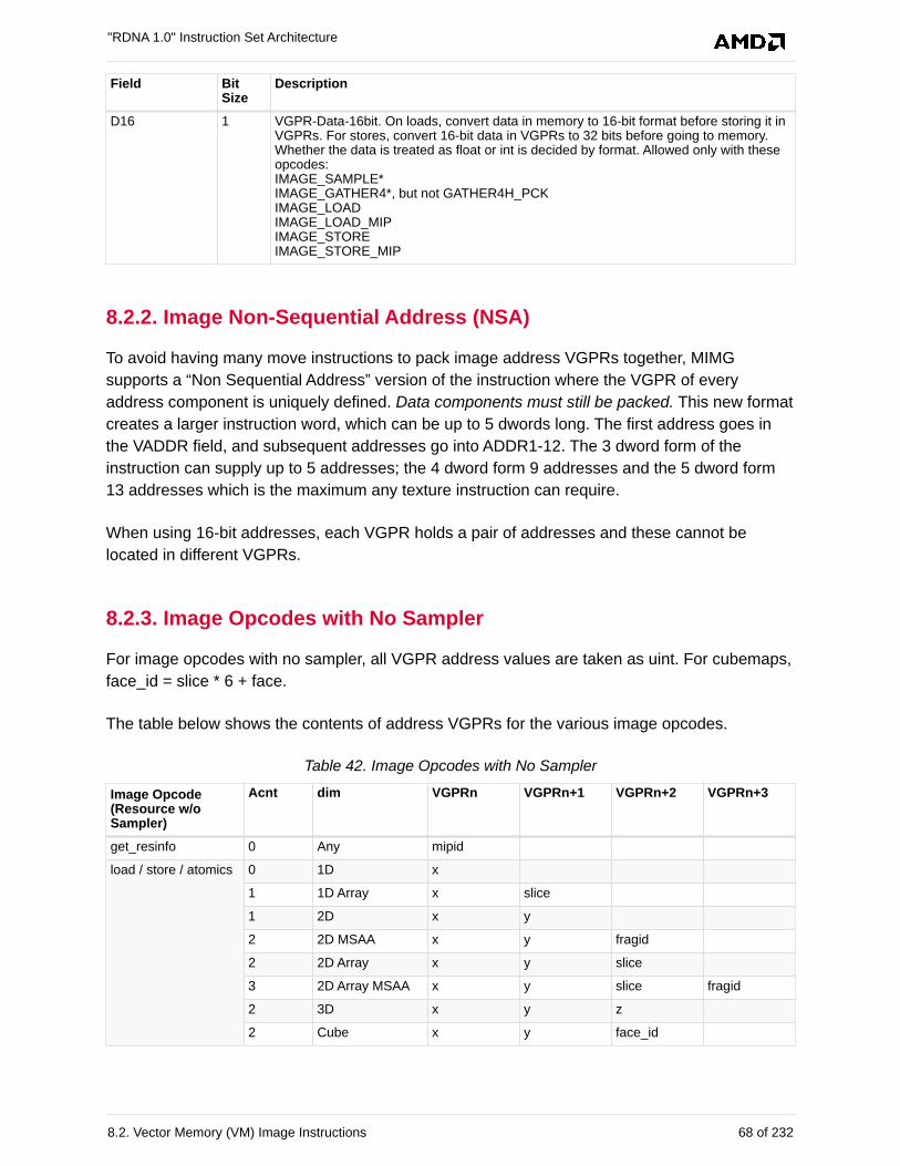
Field BitSize
Description
D16 1 VGPR-Data-16bit. On loads, convert data in memory to 16-bit format before storing it inVGPRs. For stores, convert 16-bit data in VGPRs to 32 bits before going to memory.Whether the data is treated as float or int is decided by format. Allowed only with theseopcodes:IMAGE_SAMPLE*IMAGE_GATHER4*, but not GATHER4H_PCKIMAGE_LOADIMAGE_LOAD_MIPIMAGE_STOREIMAGE_STORE_MIP
8.2.2. Image Non-Sequential Address (NSA)
To avoid having many move instructions to pack image address VGPRs together, MIMG
supports a “Non Sequential Address” version of the instruction where the VGPR of every
address component is uniquely defined. Data components must still be packed. This new format
creates a larger instruction word, which can be up to 5 dwords long. The first address goes in
the VADDR field, and subsequent addresses go into ADDR1-12. The 3 dword form of the
instruction can supply up to 5 addresses; the 4 dword form 9 addresses and the 5 dword form
13 addresses which is the maximum any texture instruction can require.
When using 16-bit addresses, each VGPR holds a pair of addresses and these cannot be
located in different VGPRs.
8.2.3. Image Opcodes with No Sampler
For image opcodes with no sampler, all VGPR address values are taken as uint. For cubemaps,
face_id = slice * 6 + face.
The table below shows the contents of address VGPRs for the various image opcodes.
Table 42. Image Opcodes with No Sampler
Image Opcode(Resource w/oSampler)
Acnt dim VGPRn VGPRn+1 VGPRn+2 VGPRn+3
get_resinfo 0 Any mipid
load / store / atomics 0 1D x
1 1D Array x slice
1 2D x y
2 2D MSAA x y fragid
2 2D Array x y slice
3 2D Array MSAA x y slice fragid
2 3D x y z
2 Cube x y face_id
"RDNA 1.0" Instruction Set Architecture
8.2. Vector Memory (VM) Image Instructions 68 of 232
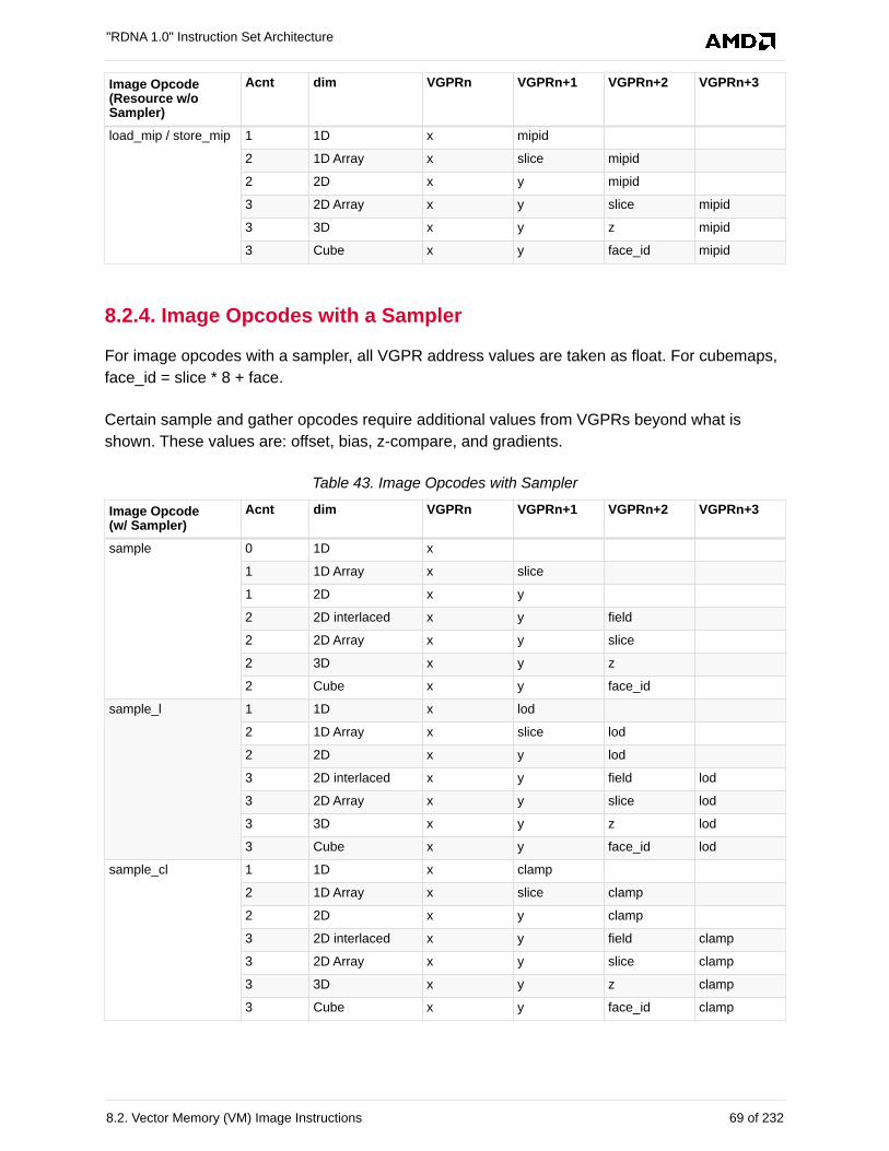
Image Opcode(Resource w/oSampler)
Acnt dim VGPRn VGPRn+1 VGPRn+2 VGPRn+3
load_mip / store_mip 1 1D x mipid
2 1D Array x slice mipid
2 2D x y mipid
3 2D Array x y slice mipid
3 3D x y z mipid
3 Cube x y face_id mipid
8.2.4. Image Opcodes with a Sampler
For image opcodes with a sampler, all VGPR address values are taken as float. For cubemaps,
face_id = slice * 8 + face.
Certain sample and gather opcodes require additional values from VGPRs beyond what is
shown. These values are: offset, bias, z-compare, and gradients.
Table 43. Image Opcodes with Sampler
Image Opcode(w/ Sampler)
Acnt dim VGPRn VGPRn+1 VGPRn+2 VGPRn+3
sample 0 1D x
1 1D Array x slice
1 2D x y
2 2D interlaced x y field
2 2D Array x y slice
2 3D x y z
2 Cube x y face_id
sample_l 1 1D x lod
2 1D Array x slice lod
2 2D x y lod
3 2D interlaced x y field lod
3 2D Array x y slice lod
3 3D x y z lod
3 Cube x y face_id lod
sample_cl 1 1D x clamp
2 1D Array x slice clamp
2 2D x y clamp
3 2D interlaced x y field clamp
3 2D Array x y slice clamp
3 3D x y z clamp
3 Cube x y face_id clamp
"RDNA 1.0" Instruction Set Architecture
8.2. Vector Memory (VM) Image Instructions 69 of 232
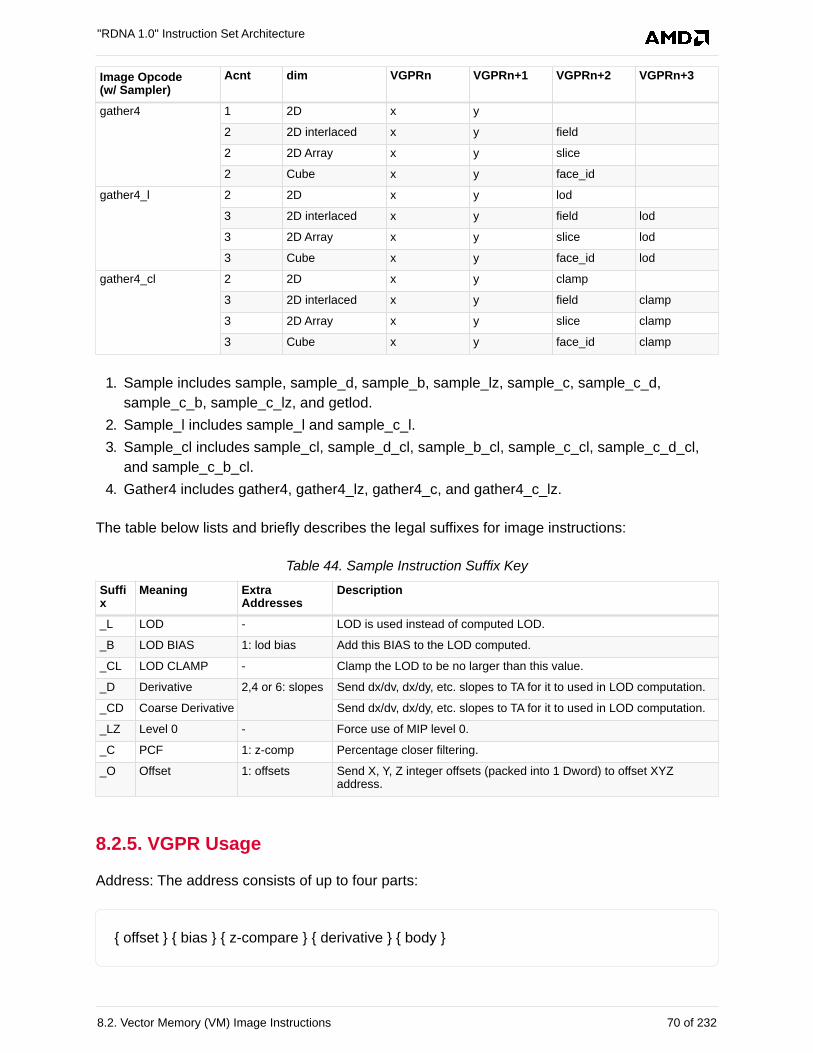
Image Opcode(w/ Sampler)
Acnt dim VGPRn VGPRn+1 VGPRn+2 VGPRn+3
gather4 1 2D x y
2 2D interlaced x y field
2 2D Array x y slice
2 Cube x y face_id
gather4_l 2 2D x y lod
3 2D interlaced x y field lod
3 2D Array x y slice lod
3 Cube x y face_id lod
gather4_cl 2 2D x y clamp
3 2D interlaced x y field clamp
3 2D Array x y slice clamp
3 Cube x y face_id clamp
1. Sample includes sample, sample_d, sample_b, sample_lz, sample_c, sample_c_d,
sample_c_b, sample_c_lz, and getlod.
2. Sample_l includes sample_l and sample_c_l.
3. Sample_cl includes sample_cl, sample_d_cl, sample_b_cl, sample_c_cl, sample_c_d_cl,
and sample_c_b_cl.
4. Gather4 includes gather4, gather4_lz, gather4_c, and gather4_c_lz.
The table below lists and briefly describes the legal suffixes for image instructions:
Table 44. Sample Instruction Suffix Key
Suffix
Meaning ExtraAddresses
Description
_L LOD - LOD is used instead of computed LOD.
_B LOD BIAS 1: lod bias Add this BIAS to the LOD computed.
_CL LOD CLAMP - Clamp the LOD to be no larger than this value.
_D Derivative 2,4 or 6: slopes Send dx/dv, dx/dy, etc. slopes to TA for it to used in LOD computation.
_CD Coarse Derivative Send dx/dv, dx/dy, etc. slopes to TA for it to used in LOD computation.
_LZ Level 0 - Force use of MIP level 0.
_C PCF 1: z-comp Percentage closer filtering.
_O Offset 1: offsets Send X, Y, Z integer offsets (packed into 1 Dword) to offset XYZaddress.
8.2.5. VGPR Usage
Address: The address consists of up to four parts:
{ offset } { bias } { z-compare } { derivative } { body }
"RDNA 1.0" Instruction Set Architecture
8.2. Vector Memory (VM) Image Instructions 70 of 232
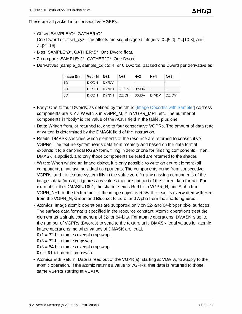
These are all packed into consecutive VGPRs.
• Offset: SAMPLE*O*, GATHER*O*
One Dword of offset_xyz. The offsets are six-bit signed integers: X=[5:0], Y=[13:8], and
Z=[21:16].
• Bias: SAMPLE*B*, GATHER*B*. One Dword float.
• Z-compare: SAMPLE*C*, GATHER*C*. One Dword.
• Derivatives (sample_d, sample_cd): 2, 4, or 6 Dwords, packed one Dword per derivative as:
Image Dim Vgpr N N+1 N+2 N+3 N+4 N+5
1D DX/DH DX/DV - - - -
2D DX/DH DY/DH DX/DV DY/DV - -
3D DX/DH DY/DH DZ/DH DX/DV DY/DV DZ/DV
• Body: One to four Dwords, as defined by the table: [Image Opcodes with Sampler] Address
components are X,Y,Z,W with X in VGPR_M, Y in VGPR_M+1, etc. The number of
components in "body" is the value of the ACNT field in the table, plus one.
• Data: Written from, or returned to, one to four consecutive VGPRs. The amount of data read
or written is determined by the DMASK field of the instruction.
• Reads: DMASK specifies which elements of the resource are returned to consecutive
VGPRs. The texture system reads data from memory and based on the data format
expands it to a canonical RGBA form, filling in zero or one for missing components. Then,
DMASK is applied, and only those components selected are returned to the shader.
• Writes: When writing an image object, it is only possible to write an entire element (all
components), not just individual components. The components come from consecutive
VGPRs, and the texture system fills in the value zero for any missing components of the
image’s data format; it ignores any values that are not part of the stored data format. For
example, if the DMASK=1001, the shader sends Red from VGPR_N, and Alpha from
VGPR_N+1, to the texture unit. If the image object is RGB, the texel is overwritten with Red
from the VGPR_N, Green and Blue set to zero, and Alpha from the shader ignored.
• Atomics: Image atomic operations are supported only on 32- and 64-bit-per pixel surfaces.
The surface data format is specified in the resource constant. Atomic operations treat the
element as a single component of 32- or 64-bits. For atomic operations, DMASK is set to
the number of VGPRs (Dwords) to send to the texture unit. DMASK legal values for atomic
image operations: no other values of DMASK are legal.
0x1 = 32-bit atomics except cmpswap.
0x3 = 32-bit atomic cmpswap.
0x3 = 64-bit atomics except cmpswap.
0xf = 64-bit atomic cmpswap.
• Atomics with Return: Data is read out of the VGPR(s), starting at VDATA, to supply to the
atomic operation. If the atomic returns a value to VGPRs, that data is returned to those
same VGPRs starting at VDATA.
"RDNA 1.0" Instruction Set Architecture
8.2. Vector Memory (VM) Image Instructions 71 of 232
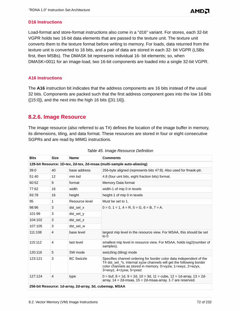
D16 Instructions
Load-format and store-format instructions also come in a "d16" variant. For stores, each 32-bit
VGPR holds two 16-bit data elements that are passed to the texture unit. The texture unit
converts them to the texture format before writing to memory. For loads, data returned from the
texture unit is converted to 16 bits, and a pair of data are stored in each 32- bit VGPR (LSBs
first, then MSBs). The DMASK bit represents individual 16- bit elements; so, when
DMASK=0011 for an image-load, two 16-bit components are loaded into a single 32-bit VGPR.
A16 Instructions
The A16 instruction bit indicates that the address components are 16 bits instead of the usual
32 bits. Components are packed such that the first address component goes into the low 16 bits
([15:0]), and the next into the high 16 bits ([31:16]).
8.2.6. Image Resource
The image resource (also referred to as T#) defines the location of the image buffer in memory,
its dimensions, tiling, and data format. These resources are stored in four or eight consecutive
SGPRs and are read by MIMG instructions.
Table 45. Image Resource Definition
Bits Size Name Comments
128-bit Resource: 1D-tex, 2d-tex, 2d-msaa (multi-sample auto-aliasing)
39:0 40 base address 256-byte aligned (represents bits 47:8). Also used for fmask-ptr.
51:40 12 min lod 4.8 (four uint bits, eight fraction bits) format.
60:52 9 format Memory Data format
77:62 16 width width-1 of mip 0 in texels
93:78 16 height height-1 of mip 0 in texels
95 1 Resource level Must be set to 1.
98:96 3 dst_sel_x 0 = 0, 1 = 1, 4 = R, 5 = G, 6 = B, 7 = A.
101:99 3 dst_sel_y
104:102 3 dst_sel_z
107:105 3 dst_sel_w
111:108 4 base level largest mip level in the resource view. For MSAA, this should be setto 0
115:112 4 last level smallest mip level in resource view. For MSAA, holds log2(number ofsamples).
120:116 5 SW mode swizzling (tiling) mode
123:121 3 BC Swizzle Specifies channel ordering for border color data independent of theT# dst_sel_*s. Internal xyzw channels will get the following bordercolor channels as stored in memory. 0=xyzw, 1=xwyz, 2=wzyx,3=wxyz, 4=zyxw, 5=yxwz
127:124 4 type 0 = buf, 8 = 1d, 9 = 2d, 10 = 3d, 11 = cube, 12 = 1d-array, 13 = 2d-array, 14 = 2d-msaa, 15 = 2d-msaa-array. 1-7 are reserved.
256-bit Resource: 1d-array, 2d-array, 3d, cubemap, MSAA
"RDNA 1.0" Instruction Set Architecture
8.2. Vector Memory (VM) Image Instructions 72 of 232
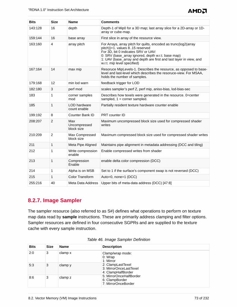
Bits Size Name Comments
143:128 16 depth Depth-1 of Mip0 for a 3D map; last array slice for a 2D-array or 1D-array or cube-map.
159:144 16 base array First slice in array of the resource view.
163:160 4 array pitch For Arrays, array pitch for quilts, encoded as trunc(log2(arraypitch))+1. values 8..15 reservedFor 3D, bit 0 indicates SRV or UAV:0: SRV (base_array ignored, depth w.r.t. base map)1: UAV (base_array and depth are first and last layer in view, andw.r.t. mip level specified)
167:164 14 max mip Resoruce MipLevels-1. Describes the resource, as opposed to base-level and last-level which describes the resoruce-view. For MSAA,holds the number of samples.
179:168 12 min lod warn feedback trigger for LOD
182:180 3 perf mod scales sampler’s perf Z, perf mip, aniso-bias, lod-bias-sec
183 1 corner samplesmod
Describes how texels were generated in the resource. 0=centersampled, 1 = corner sampled.
185 1 LOD hardwarecount enable
Partially resident texture hardware counter enable
199:192 8 Counter Bank ID PRT counter ID
208:207 2 MaxUncompressedblock size
Maximum uncompressed block size used for compressed shaderwrites
210:209 2 Max Compressedblock size
Maximum compressed block size used for compressed shader writes
211 1 Meta Pipe Aligned Maintains pipe alignment in metadata addressing (DCC and tiling)
212 1 Write compressionenable
Enable compressed writes from shader
213 1 CompressionEnable
enable delta color compression (DCC)
214 1 Alpha is on MSB Set to 1 if the surface’s component swap is not reversed (DCC)
215 1 Color Transform Auto=0, none=1 (DCC)
255:216 40 Meta Data Address Upper bits of meta-data address (DCC) [47:8]
8.2.7. Image Sampler
The sampler resource (also referred to as S#) defines what operations to perform on texture
map data read by sample instructions. These are primarily address clamping and filter options.
Sampler resources are defined in four consecutive SGPRs and are supplied to the texture
cache with every sample instruction.
Table 46. Image Sampler Definition
Bits Size Name Description
2:0 3 clamp x Clamp/wrap mode:0: Wrap1: Mirror2: ClampLastTexel3: MirrorOnceLastTexel4: ClampHalfBorder5: MirrorOnceHalfBorder6: ClampBorder7: MirrorOnceBorder
5:3 3 clamp y
8:6 3 clamp z
"RDNA 1.0" Instruction Set Architecture
8.2. Vector Memory (VM) Image Instructions 73 of 232
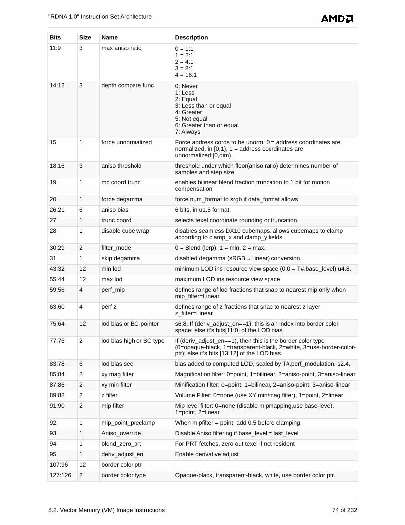
Bits Size Name Description
11:9 3 max aniso ratio 0 = 1:11 = 2:12 = 4:13 = 8:14 = 16:1
14:12 3 depth compare func 0: Never1: Less2: Equal3: Less than or equal4: Greater5: Not equal6: Greater than or equal7: Always
15 1 force unnormalized Force address cords to be unorm: 0 = address coordinates arenormalized, in [0,1); 1 = address coordinates areunnormalized:[0,dim).
18:16 3 aniso threshold threshold under which floor(aniso ratio) determines number ofsamples and step size
19 1 mc coord trunc enables bilinear blend fraction truncation to 1 bit for motioncompensation
20 1 force degamma force num_format to srgb if data_format allows
26:21 6 aniso bias 6 bits, in u1.5 format.
27 1 trunc coord selects texel coordinate rounding or truncation.
28 1 disable cube wrap disables seamless DX10 cubemaps, allows cubemaps to clampaccording to clamp_x and clamp_y fields
30:29 2 filter_mode 0 = Blend (lerp); 1 = min, 2 = max.
31 1 skip degamma disabled degamma (sRGB→Linear) conversion.
43:32 12 min lod minimum LOD ins resource view space (0.0 = T#.base_level) u4.8.
55:44 12 max lod maximum LOD ins resource view space
59:56 4 perf_mip defines range of lod fractions that snap to nearest mip only whenmip_filter=Linear
63:60 4 perf z defines range of z fractions that snap to nearest z layerz_filter=Linear
75:64 12 lod bias or BC-pointer s6.8. If (deriv_adjust_en==1), this is an index into border colorspace; else it’s bits[11:0] of the LOD bias.
77:76 2 lod bias high or BC type If (deriv_adjust_en==1), then this is the border color type(0=opaque-black, 1=transparent-black, 2=white, 3=use-border-color-ptr); else it’s bits [13:12] of the LOD bias.
83:78 6 lod bias sec bias added to computed LOD, scaled by T#.perf_modulation. s2.4.
85:84 2 xy mag filter Magnification filter: 0=point, 1=bilinear, 2=aniso-point, 3=aniso-linear
87:86 2 xy min filter Minification filter: 0=point, 1=bilinear, 2=aniso-point, 3=aniso-linear
89:88 2 z filter Volume Filter: 0=none (use XY min/mag filter), 1=point, 2=linear
91:90 2 mip filter Mip level filter: 0=none (disable mipmapping,use base-leve),1=point, 2=linear
92 1 mip_point_preclamp When mipfilter = point, add 0.5 before clamping.
93 1 Aniso_override Disable Aniso filtering if base_level = last_level
94 1 blend_zero_prt For PRT fetches, zero out texel if not resident
95 1 deriv_adjust_en Enable derivative adjust
107:96 12 border color ptr
127:126 2 border color type Opaque-black, transparent-black, white, use border color ptr.
"RDNA 1.0" Instruction Set Architecture
8.2. Vector Memory (VM) Image Instructions 74 of 232
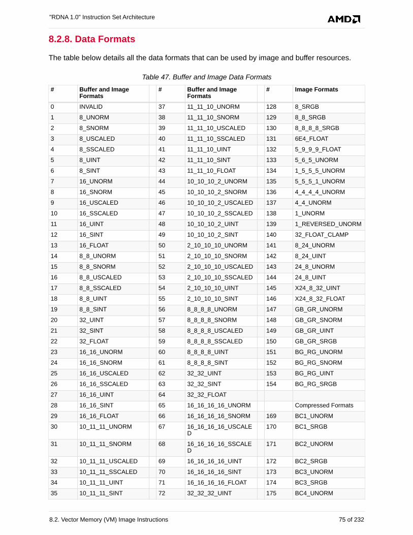
8.2.8. Data Formats
The table below details all the data formats that can be used by image and buffer resources.
Table 47. Buffer and Image Data Formats
# Buffer and ImageFormats
# Buffer and ImageFormats
# Image Formats
0 INVALID 37 11_11_10_UNORM 128 8_SRGB
1 8_UNORM 38 11_11_10_SNORM 129 8_8_SRGB
2 8_SNORM 39 11_11_10_USCALED 130 8_8_8_8_SRGB
3 8_USCALED 40 11_11_10_SSCALED 131 6E4_FLOAT
4 8_SSCALED 41 11_11_10_UINT 132 5_9_9_9_FLOAT
5 8_UINT 42 11_11_10_SINT 133 5_6_5_UNORM
6 8_SINT 43 11_11_10_FLOAT 134 1_5_5_5_UNORM
7 16_UNORM 44 10_10_10_2_UNORM 135 5_5_5_1_UNORM
8 16_SNORM 45 10_10_10_2_SNORM 136 4_4_4_4_UNORM
9 16_USCALED 46 10_10_10_2_USCALED 137 4_4_UNORM
10 16_SSCALED 47 10_10_10_2_SSCALED 138 1_UNORM
11 16_UINT 48 10_10_10_2_UINT 139 1_REVERSED_UNORM
12 16_SINT 49 10_10_10_2_SINT 140 32_FLOAT_CLAMP
13 16_FLOAT 50 2_10_10_10_UNORM 141 8_24_UNORM
14 8_8_UNORM 51 2_10_10_10_SNORM 142 8_24_UINT
15 8_8_SNORM 52 2_10_10_10_USCALED 143 24_8_UNORM
16 8_8_USCALED 53 2_10_10_10_SSCALED 144 24_8_UINT
17 8_8_SSCALED 54 2_10_10_10_UINT 145 X24_8_32_UINT
18 8_8_UINT 55 2_10_10_10_SINT 146 X24_8_32_FLOAT
19 8_8_SINT 56 8_8_8_8_UNORM 147 GB_GR_UNORM
20 32_UINT 57 8_8_8_8_SNORM 148 GB_GR_SNORM
21 32_SINT 58 8_8_8_8_USCALED 149 GB_GR_UINT
22 32_FLOAT 59 8_8_8_8_SSCALED 150 GB_GR_SRGB
23 16_16_UNORM 60 8_8_8_8_UINT 151 BG_RG_UNORM
24 16_16_SNORM 61 8_8_8_8_SINT 152 BG_RG_SNORM
25 16_16_USCALED 62 32_32_UINT 153 BG_RG_UINT
26 16_16_SSCALED 63 32_32_SINT 154 BG_RG_SRGB
27 16_16_UINT 64 32_32_FLOAT
28 16_16_SINT 65 16_16_16_16_UNORM Compressed Formats
29 16_16_FLOAT 66 16_16_16_16_SNORM 169 BC1_UNORM
30 10_11_11_UNORM 67 16_16_16_16_USCALED
170 BC1_SRGB
31 10_11_11_SNORM 68 16_16_16_16_SSCALED
171 BC2_UNORM
32 10_11_11_USCALED 69 16_16_16_16_UINT 172 BC2_SRGB
33 10_11_11_SSCALED 70 16_16_16_16_SINT 173 BC3_UNORM
34 10_11_11_UINT 71 16_16_16_16_FLOAT 174 BC3_SRGB
35 10_11_11_SINT 72 32_32_32_UINT 175 BC4_UNORM
"RDNA 1.0" Instruction Set Architecture
8.2. Vector Memory (VM) Image Instructions 75 of 232
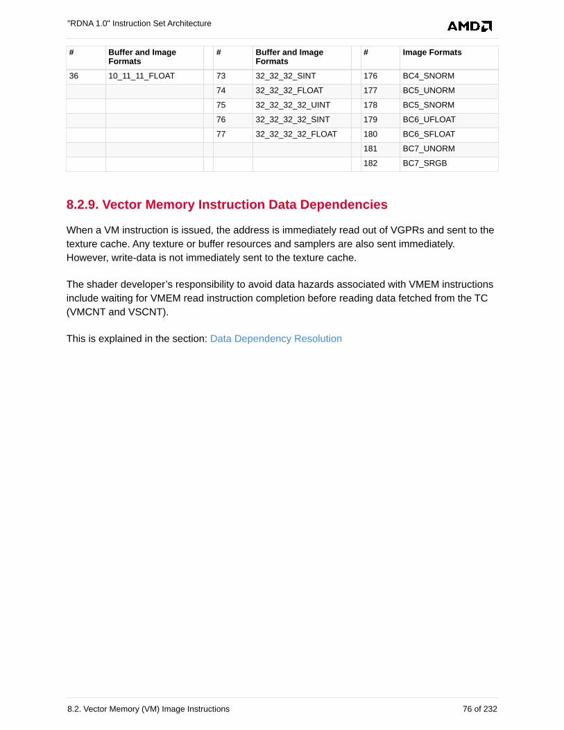
# Buffer and ImageFormats
# Buffer and ImageFormats
# Image Formats
36 10_11_11_FLOAT 73 32_32_32_SINT 176 BC4_SNORM
74 32_32_32_FLOAT 177 BC5_UNORM
75 32_32_32_32_UINT 178 BC5_SNORM
76 32_32_32_32_SINT 179 BC6_UFLOAT
77 32_32_32_32_FLOAT 180 BC6_SFLOAT
181 BC7_UNORM
182 BC7_SRGB
8.2.9. Vector Memory Instruction Data Dependencies
When a VM instruction is issued, the address is immediately read out of VGPRs and sent to the
texture cache. Any texture or buffer resources and samplers are also sent immediately.
However, write-data is not immediately sent to the texture cache.
The shader developer’s responsibility to avoid data hazards associated with VMEM instructions
include waiting for VMEM read instruction completion before reading data fetched from the TC
(VMCNT and VSCNT).
This is explained in the section: Data Dependency Resolution
"RDNA 1.0" Instruction Set Architecture
8.2. Vector Memory (VM) Image Instructions 76 of 232
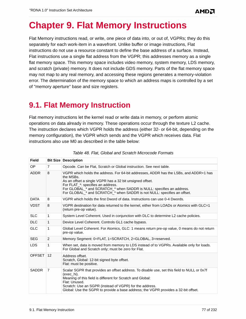
Chapter 9. Flat Memory Instructions
Flat Memory instructions read, or write, one piece of data into, or out of, VGPRs; they do this
separately for each work-item in a wavefront. Unlike buffer or image instructions, Flat
instructions do not use a resource constant to define the base address of a surface. Instead,
Flat instructions use a single flat address from the VGPR; this addresses memory as a single
flat memory space. This memory space includes video memory, system memory, LDS memory,
and scratch (private) memory. It does not include GDS memory. Parts of the flat memory space
may not map to any real memory, and accessing these regions generates a memory-violation
error. The determination of the memory space to which an address maps is controlled by a set
of "memory aperture" base and size registers.
9.1. Flat Memory Instruction
Flat memory instructions let the kernel read or write data in memory, or perform atomic
operations on data already in memory. These operations occur through the texture L2 cache.
The instruction declares which VGPR holds the address (either 32- or 64-bit, depending on the
memory configuration), the VGPR which sends and the VGPR which receives data. Flat
instructions also use M0 as described in the table below:
Table 48. Flat, Global and Scratch Microcode Formats
Field Bit Size Description
OP 7 Opcode. Can be Flat, Scratch or Global instruction. See next table.
ADDR 8 VGPR which holds the address. For 64-bit addresses, ADDR has the LSBs, and ADDR+1 hasthe MSBs.As an offset a single VGPR has a 32 bit unsigned offset.For FLAT_*: specifies an address.For GLOBAL_* and SCRATCH_* when SADDR is NULL: specifies an address.For GLOBAL_* and SCRATCH_* when SADDR is not NULL: specifies an offset.
DATA 8 VGPR which holds the first Dword of data. Instructions can use 0-4 Dwords.
VDST 8 VGPR destination for data returned to the kernel, either from LOADs or Atomics with GLC=1(return pre-op value).
SLC 1 System Level Coherent. Used in conjunction with DLC to determine L2 cache policies.
DLC 1 Device Level Coherent. Controls GL1 cache bypass.
GLC 1 Global Level Coherent. For Atomics, GLC: 1 means return pre-op value, 0 means do not returnpre-op value.
SEG 2 Memory Segment: 0=FLAT, 1=SCRATCH, 2=GLOBAL, 3=reserved.
LDS 1 When set, data is moved from memory to LDS instead of to VGPRs. Available only for loads.For Global and Scratch only; must be zero for Flat.
OFFSET 12 Address offset.Scratch, Global: 12-bit signed byte offset.Flat: must be positive.
SADDR 7 Scalar SGPR that provides an offset address. To disable use, set this field to NULL or 0x7f(exec_hi).Meaning of this field is different for Scratch and Global:Flat: Unused.Scratch: Use an SGPR (instead of VGPR) for the address.Global: Use the SGPR to provide a base address; the VGPR provides a 32-bit offset.
"RDNA 1.0" Instruction Set Architecture
9.1. Flat Memory Instruction 77 of 232
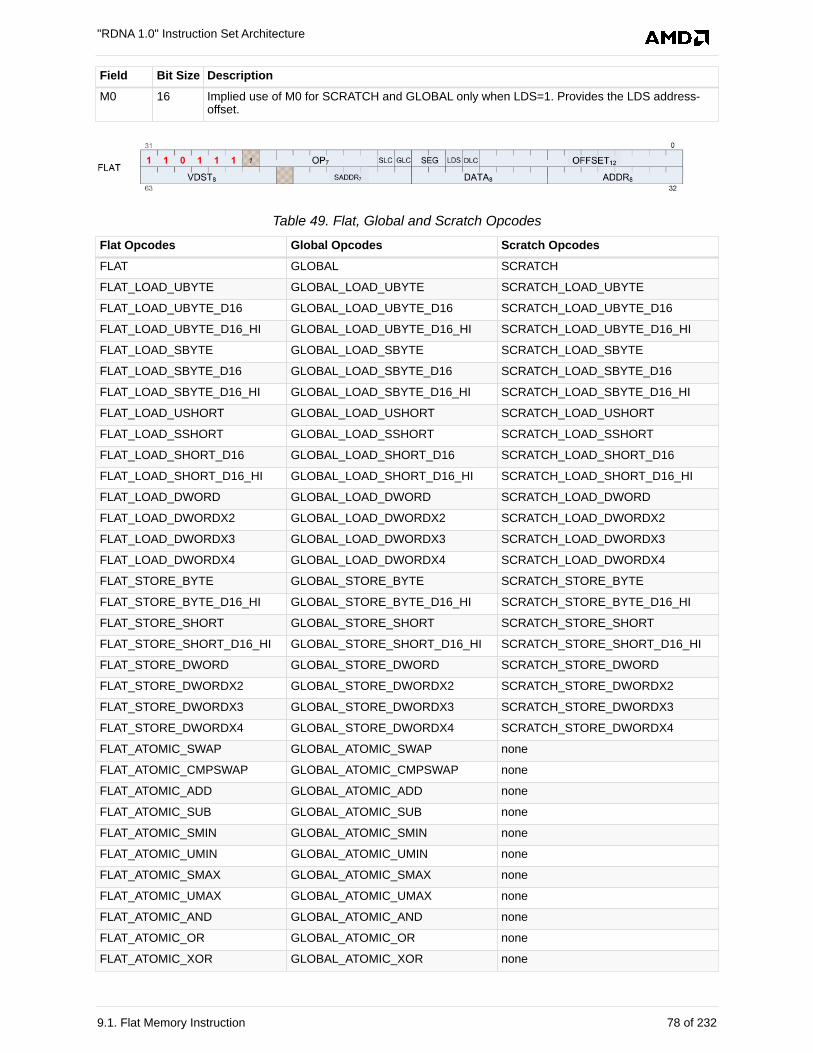
Field Bit Size Description
M0 16 Implied use of M0 for SCRATCH and GLOBAL only when LDS=1. Provides the LDS address-offset.
Table 49. Flat, Global and Scratch Opcodes
Flat Opcodes Global Opcodes Scratch Opcodes
FLAT GLOBAL SCRATCH
FLAT_LOAD_UBYTE GLOBAL_LOAD_UBYTE SCRATCH_LOAD_UBYTE
FLAT_LOAD_UBYTE_D16 GLOBAL_LOAD_UBYTE_D16 SCRATCH_LOAD_UBYTE_D16
FLAT_LOAD_UBYTE_D16_HI GLOBAL_LOAD_UBYTE_D16_HI SCRATCH_LOAD_UBYTE_D16_HI
FLAT_LOAD_SBYTE GLOBAL_LOAD_SBYTE SCRATCH_LOAD_SBYTE
FLAT_LOAD_SBYTE_D16 GLOBAL_LOAD_SBYTE_D16 SCRATCH_LOAD_SBYTE_D16
FLAT_LOAD_SBYTE_D16_HI GLOBAL_LOAD_SBYTE_D16_HI SCRATCH_LOAD_SBYTE_D16_HI
FLAT_LOAD_USHORT GLOBAL_LOAD_USHORT SCRATCH_LOAD_USHORT
FLAT_LOAD_SSHORT GLOBAL_LOAD_SSHORT SCRATCH_LOAD_SSHORT
FLAT_LOAD_SHORT_D16 GLOBAL_LOAD_SHORT_D16 SCRATCH_LOAD_SHORT_D16
FLAT_LOAD_SHORT_D16_HI GLOBAL_LOAD_SHORT_D16_HI SCRATCH_LOAD_SHORT_D16_HI
FLAT_LOAD_DWORD GLOBAL_LOAD_DWORD SCRATCH_LOAD_DWORD
FLAT_LOAD_DWORDX2 GLOBAL_LOAD_DWORDX2 SCRATCH_LOAD_DWORDX2
FLAT_LOAD_DWORDX3 GLOBAL_LOAD_DWORDX3 SCRATCH_LOAD_DWORDX3
FLAT_LOAD_DWORDX4 GLOBAL_LOAD_DWORDX4 SCRATCH_LOAD_DWORDX4
FLAT_STORE_BYTE GLOBAL_STORE_BYTE SCRATCH_STORE_BYTE
FLAT_STORE_BYTE_D16_HI GLOBAL_STORE_BYTE_D16_HI SCRATCH_STORE_BYTE_D16_HI
FLAT_STORE_SHORT GLOBAL_STORE_SHORT SCRATCH_STORE_SHORT
FLAT_STORE_SHORT_D16_HI GLOBAL_STORE_SHORT_D16_HI SCRATCH_STORE_SHORT_D16_HI
FLAT_STORE_DWORD GLOBAL_STORE_DWORD SCRATCH_STORE_DWORD
FLAT_STORE_DWORDX2 GLOBAL_STORE_DWORDX2 SCRATCH_STORE_DWORDX2
FLAT_STORE_DWORDX3 GLOBAL_STORE_DWORDX3 SCRATCH_STORE_DWORDX3
FLAT_STORE_DWORDX4 GLOBAL_STORE_DWORDX4 SCRATCH_STORE_DWORDX4
FLAT_ATOMIC_SWAP GLOBAL_ATOMIC_SWAP none
FLAT_ATOMIC_CMPSWAP GLOBAL_ATOMIC_CMPSWAP none
FLAT_ATOMIC_ADD GLOBAL_ATOMIC_ADD none
FLAT_ATOMIC_SUB GLOBAL_ATOMIC_SUB none
FLAT_ATOMIC_SMIN GLOBAL_ATOMIC_SMIN none
FLAT_ATOMIC_UMIN GLOBAL_ATOMIC_UMIN none
FLAT_ATOMIC_SMAX GLOBAL_ATOMIC_SMAX none
FLAT_ATOMIC_UMAX GLOBAL_ATOMIC_UMAX none
FLAT_ATOMIC_AND GLOBAL_ATOMIC_AND none
FLAT_ATOMIC_OR GLOBAL_ATOMIC_OR none
FLAT_ATOMIC_XOR GLOBAL_ATOMIC_XOR none
"RDNA 1.0" Instruction Set Architecture
9.1. Flat Memory Instruction 78 of 232
Flat Opcodes Global Opcodes Scratch Opcodes
FLAT_ATOMIC_INC GLOBAL_ATOMIC_INC none
FLAT_ATOMIC_DEC GLOBAL_ATOMIC_DEC none
FLAT_ATOMIC_FMIN GLOBAL_ATOMIC_FMIN none
FLAT_ATOMIC_FMAX GLOBAL_ATOMIC_FMAX none
FLAT_ATOMIC_FCMPSWAP GLOBAL_ATOMIC_FCMPSWAP none
The atomic instructions above are also available in "_X2" versions (64-bit).
9.2. Instructions
The FLAT instruction set is nearly identical to the Buffer instruction set, but without the FORMAT
reads and writes. Unlike Buffer instructions, FLAT instructions cannot return data directly to
LDS, but only to VGPRs.
FLAT instructions do not use a resource constant (V#) or sampler (S#); however, they do require
a additional register (FLAT_SCRATCH) to hold scratch-space memory address information in
case any threads' address resolves to scratch space. See the scratch section for details.
Internally, FLAT instruction are executed as both an LDS and a Buffer instruction; so, they
increment both VM_CNT/VS_CNT and LGKM_CNT and are not considered done until both
have been decremented. There is no way beforehand to determine whether a FLAT instruction
uses only LDS or texture memory space.
9.2.1. Ordering
Flat instructions can complete out of order with each other. If one flat instruction finds all of its
data in Texture cache, and the next finds all of its data in LDS, the second instruction might
complete first. If the two fetches return data to the same VGPR, the result are unknown.
9.2.2. Importing Timing Consideration
Since the data for a FLAT load can come from either LDS or the texture cache, and because
these units have different latencies, there is a potential race condition with respect to the
VM_CNT/VS_CNT and LGKM_CNT counters. Because of this, the only sensible S_WAITCNT
value to use after FLAT instructions is zero.
9.3. Addressing
FLAT instructions support both 64- and 32-bit addressing. The address size is set using a mode
register (PTR32), and a local copy of the value is stored per wave.
The addresses for the aperture check differ in 32- and 64-bit mode; however, this is not covered
"RDNA 1.0" Instruction Set Architecture
9.2. Instructions 79 of 232
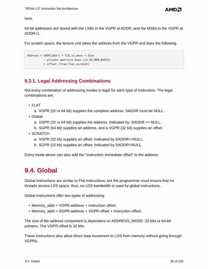
here.
64-bit addresses are stored with the LSBs in the VGPR at ADDR, and the MSBs in the VGPR at
ADDR+1.
For scratch space, the texture unit takes the address from the VGPR and does the following.
Address = VGPR[addr] + TID_in_wave * Size - private aperture base (in SH_MEM_BASES) + offset (from flat_scratch)
9.3.1. Legal Addressing Combinations
Not every combination of addressing modes is legal for each type of instruction. The legal
combinations are:
• FLAT
a. VGPR (32 or 64 bit) supplies the complete address. SADDR must be NULL.
• Global
a. VGPR (32 or 64 bit) supplies the address. Indicated by: SADDR == NULL.
b. SGPR (64 bit) supplies an address, and a VGPR (32 bit) supplies an offset
• SCRATCH
a. VGPR (32 bit) supplies an offset. Indicated by SADDR==NULL.
b. SGPR (32 bit) supplies an offset. Indicated by SADDR!=NULL.
Every mode above can also add the "instruction immediate offset" to the address.
9.4. Global
Global instructions are similar to Flat instructions, but the programmer must ensure that no
threads access LDS space; thus, no LDS bandwidth is used by global instructions.
Global instructions offer two types of addressing:
• Memory_addr = VGPR-address + instruction offset.
• Memory_addr = SGPR-address + VGPR-offset + instruction offset.
The size of the address component is dependent on ADDRESS_MODE: 32-bits or 64-bit
pointers. The VGPR-offset is 32 bits.
These instructions also allow direct data movement to LDS from memory without going through
VGPRs.
"RDNA 1.0" Instruction Set Architecture
9.4. Global 80 of 232
Since these instructions do not access LDS, only VM_CNT/VS_CNT is used, not LGKM_CNT. If
a global instruction does attempt to access LDS, the instruction returns MEM_VIOL.
9.5. Scratch
Scratch instructions are similar to Flat, but the programmer must ensure that no threads access
LDS space, and the memory space is swizzled. Thus, no LDS bandwidth is used by scratch
instructions.
Scratch instructions also support multi-Dword access and mis-aligned access (although mis-
aligned is slower).
Scratch instructions use the following addressing:
• Memory_addr = flat_scratch.addr + swizzle(V/SGPR_offset + inst_offset, threadID)
The offset can come from either an SGPR or a VGPR, and is a 32- bit unsigned byte.
The size of the address component is dependent on the ADDRESS_MODE: 32-bits or 64-bit
pointers. The VGPR-offset is 32 bits.
These instructions also allow direct data movement to LDS from memory without going through
VGPRs.
Since these instructions do not access LDS, only VM_CNT/VS_CNT is used, not LGKM_CNT. It
is not possible for a Scratch instruction to access LDS; thus, no error or aperture checking is
done.
9.6. Memory Error Checking
Both the texture unit and LDS can report that an error occurred due to a bad address. This can
occur for the following reasons:
• invalid address (outside any aperture)
• write to read-only surface
• misaligned data
• out-of-range address:
◦ LDS access with an address outside the range: [ 0, MIN(M0, LDS_SIZE)-1 ]
◦ Scratch access with an address outside the range: [0, scratch-size -1 ]
The policy for threads with bad addresses is: writes outside this range do not write a value, and
reads return zero.
Addressing errors from either LDS or texture are returned on their respective "instruction done"
busses as MEM_VIOL. This sets the wave’s MEM_VIOL TrapStatus bit and causes an
"RDNA 1.0" Instruction Set Architecture
9.5. Scratch 81 of 232
exception (trap) if the corresponding EXCPEN bit is set.
9.7. Data
FLAT instructions can use zero to four consecutive Dwords of data in VGPRs and/or memory.
The DATA field determines which VGPR(s) supply source data (if any), and the VDST VGPRs
hold return data (if any). No data-format conversion is done.
“D16” instructions use only 16-bit of the VGPR instead of the full 32bits. “D16_HI” instructions
read or write only the high 16-bits, while “D16” use the low 16-bits. Scratch & Global D16 load
instructions with LDS=1 will write the entire 32-bits of LDS.
9.8. Scratch Space (Private)
Scratch (thread-private memory) is an area of memory defined by the aperture registers. When
an address falls in scratch space, additional address computation is automatically performed by
the hardware. The kernel must provide additional information for this computation to occur in the
form of the FLAT_SCRATCH register.
The wavefront must supply the scratch size and offset (for space allocated to this wave) with
every FLAT request. Prior to issuing any FLAT or Scratch instructions, the shader program must
initialize the FLAT_SCRATCH register with the base address of scratch space allocated this
wave.
FLAT_SCRATCH is a 64-bit, byte address. The shader composes the value by adding together
two separate values: the base address, which can be passed in via an initialized SGPR, or
perhaps through a constant buffer, and the per-wave allocation offset (also initialized in an
SGPR).
"RDNA 1.0" Instruction Set Architecture
9.7. Data 82 of 232
Chapter 10. Data Share Operations
Local data share (LDS) is a very low-latency, RAM scratchpad for temporary data with at least
one order of magnitude higher effective bandwidth than direct, uncached global memory. It
permits sharing of data between work-items in a work-group, as well as holding parameters for
pixel shader parameter interpolation. Unlike read-only caches, the LDS permits high-speed
write-to-read re-use of the memory space (gather/read/load and scatter/write/store operations).
10.1. Overview
The figure below shows the conceptual framework of the LDS is integration into the memory of
AMD GPUs using OpenCL.
Figure 10. High-Level Memory Configuration
Physically located on-chip, directly adjacent to the ALUs, the LDS is approximately one order of
magnitude faster than global memory (assuming no bank conflicts).
There are 128kB memory per workgroup processor split up into 64 banks of dword-wide RAMs.
These 64 banks are further sub-divided into two sets of 32-banks each where 32 of the banks
are affiliated with a pair of SIMD32’s, and the other 32 banks are affiliated with the other pair of
SIMD32’s within the WGP. Each bank is a 512x32 two-port RAM (1R/1W per clock cycle).
Dwords are placed in the banks serially, but all banks can execute a store or load
simultaneously. One work-group can request up to 64kB memory.
"RDNA 1.0" Instruction Set Architecture
10.1. Overview 83 of 232
The high bandwidth of the LDS memory is achieved not only through its proximity to the ALUs,
but also through simultaneous access to its memory banks. Thus, it is possible to concurrently
execute 32 write or read instructions, each nominally 32-bits; extended instructions,
read2/write2, can be 64-bits each. If, however, more than one access attempt is made to the
same bank at the same time, a bank conflict occurs. In this case, for indexed and atomic
operations, hardware prevents the attempted concurrent accesses to the same bank by turning
them into serial accesses. This decreases the effective bandwidth of the LDS. For increased
throughput (optimal efficiency), therefore, it is important to avoid bank conflicts. A knowledge of
request scheduling and address mapping is key to achieving this.
10.2. Dataflow in Memory Hierarchy
The figure below is a conceptual diagram of the dataflow withing the memory structure.
Data can be loaded into LDS either by transferring it from VGPRs to LDS using "DS"
instructions, or by loading in from memory. When loading from memory, the data may be loaded
into VGPRs first or for some types of loads it may be loaded directly into LDS from memory. To
store data from LDS to global memory, data is read from LDS and placed into the workitem’s
VGPRs, then written out to global memory. To make effective use of the LDS, an algorithm must
perform many operations on what is transferred between global memory and LDS.
LDS atomics are performed in the LDS hardware. (Thus, although ALUs are not directly used for
these operations, latency is incurred by the LDS executing this function.)
10.3. LDS Modes and Allocation: CU vs. WGP Mode
Workgroups of waves are dispatched in one of two modes: CU or WGP. This mode controls
whether the waves of a workgroup are distributed across just two SIMD32’s (CU mode), or
"RDNA 1.0" Instruction Set Architecture
10.2. Dataflow in Memory Hierarchy 84 of 232
across all 4 SIMD32’s (WGP mode) within a WGP.
In CU mode, waves are allocated to two SIMD32’s which share a texture memory unit, and are
allocated LDS space which is all local (on the same side) as the SIMDs. This mode can provide
higher LDS memory bandwidth than WGP mode.
In WGP mode, the waves are distributed over all 4 SIMD32’s and LDS space maybe allocated
anywhere within the LDS memory. Waves may access data on the "near" or "far" side of LDS
equally, but performance may be lower in some cases. This mode provides more ALU and
texture memory bandwidth to a single workgroup (of at least 4 waves).
10.4. LDS Access
There are 3 forms of Local Data Share access:
• Direct Read – reads a single dword from LDS and broadcasts the data as input to a vector
ALU op.
• Indexed Read/write and Atomic ops – read/write address comes from a VGPR and data
to/from VGPR.
◦ LDS-ops require up to 3 inputs: 2data+1addr and immediate return VGPR.
• Parameter Interpolation – similar to direct read but with specific addressing.
◦ Reads up to 2 parameters (P0, P1-P0) or (P2-P0) from one attribute to be supplied to a
muladd.
◦ Also supplies individual parameter read for general interpolation (or select I,J=0.0)
The following subsections describe these methods.
10.4.1. LDS Direct Reads
Direct reads are only available in LDS, not in GDS.
LDS Direct reads occur in vector ALU (VALU) instructions and allow the LDS to supply a single
DWORD value which is broadcast to all threads in the wavefront and is used as the SRC0 input
to the ALU operations. A VALU instruction indicates that input is to be supplied by LDS by using
the LDS_DIRECT for the SRC0 field.
The LDS address and data-type of the data to be read from LDS comes from the M0 register:
"RDNA 1.0" Instruction Set Architecture
10.4. LDS Access 85 of 232
LDS_addr = M0[15:0] (byte address and must be Dword aligned)DataType = M0[18:16] 0 unsigned byte 1 unsigned short 2 Dword 3 unused 4 signed byte 5 signed short
10.4.2. LDS Parameter Reads
Parameter reads are only available in LDS, not in GDS.
Pixel shaders use LDS to read vertex parameter values; the pixel shader then interpolates them
to find the per-pixel parameter values. LDS parameter reads occur when the following opcodes
are used.
• V_INTERP_P1_F32 D = P10 * S + P0 Parameter interpolation, first step.
• V_INTERP_P2_F32D = P20 * S + DParameter interpolation, second step.
• V_INTERP_MOV_F32D = {P10,P20,P0}[S]Parameter load.
The typical parameter interpolation operations involves reading three parameters: P0, P10, and
P20, and using the two barycentric coordinates, I and J, to determine the final per-pixel value:
Final value = P0 + P10 * I + P20 * J
Parameter interpolation instructions indicate the parameter attribute number (0 to 32) and the
component number (0=x, 1=y, 2=z and 3=w).
Table 50. Parameter Instruction Fields
Field Size Description
VDST 8 Destination VGPR. Also acts as source for v_interp_p2_f32.
OP 2 Opcode:0: v_interp_p1_f32 VDST = P10 * VSRC + P01: v_interp_p2_f32 VDST = P20 * VSRC + VDST2: v_interp_mov_f32 VDST = (P0, P10 or P20 selected by VSRC[1:0])P0, P10 and P20 are parameter values read from LDS
ATTR 6 Attribute number: 0 to 32.
ATTRCHAN 2 0=X, 1=Y, 2=Z, 3=W
VSRC 8 Source VGPR supplies interpolation "I" or "J" value. For OP==v_interp_mov_f32: 0=P10,1=P20, 2=P0.
( M0 ) 32 Use of the M0 register is automatic. M0 must contain: { 1’b0, new_prim_mask[15:1],lds_param_offset[15:0] }
Parameter interpolation and parameter move instructions must initialize the M0 register before
"RDNA 1.0" Instruction Set Architecture
10.4. LDS Access 86 of 232
using it. The lds_param_offset[15:0] is an address offset from the beginning of LDS storage
allocated to this wavefront to where parameters begin in LDS memory for this wavefront.
The new_prim_mask is a 15-bit mask with one bit per quad; a one in this mask indicates that
this quad begins a new primitive, a zero indicates it uses the same primitive as the previous
quad. The mask is 15 bits, not 16, since the first quad in a wavefront begins a new primitive and
so it is not included in the mask.
Parameter Interpolation on 16-bit data
The above parameter interpolation opcodes use the VINTRP microcode format, but for
interpolation on 16-bit data, the VOP3 format is used. The opcodes supported are:
Opcode Operation Description
V_INTERP_P1LL_F16 d.f32 = lds.f16 * vgpr.f32 + lds.f16 attr_word selects LDS high or low 16bits. “LL” isfor “two LDS arguments.”
V_INTERP_P2_F16 d.f16 = lds.f16 * vgpr.f32 + vgpr.f32 Final computation. attr_word selects LDS high orlow 16bits. Result is written to the 16 LSB’s of thedest-vgpr.
In the VOP3 encoding, the following fields are overloaded:
• SRC1 : this field holds the VINTERP VSRC value (I or J)
• SRC0 : this is treated as a set of bit-fields: {attr_word[1], attr_chan[2], attr[6]}
“attr_word” is a bit to select the low or high half of the LDS word. 1=high, 0=low.
10.4.3. Data Share Indexed and Atomic Access
Both LDS and GDS can perform indexed and atomic data share operations. For brevity, "LDS"
is used in the text below and, except where noted, also applies to GDS.
Indexed and atomic operations supply a unique address per work-item from the VGPRs to the
LDS, and supply or return unique data per work-item back to VGPRs. Due to the internal
banked structure of LDS, operations can complete in as little as one cycle (for wave32, or 2
cycles for wave64), or take as many 64 cycles, depending upon the number of bank conflicts
(addresses that map to the same memory bank).
Indexed operations are simple LDS load and store operations that read data from, and return
data to, VGPRs.
Atomic operations are arithmetic operations that combine data from VGPRs and data in LDS,
and write the result back to LDS. Atomic operations have the option of returning the LDS "pre-
op" value to VGPRs.
The table below lists and briefly describes the LDS instruction fields.
"RDNA 1.0" Instruction Set Architecture
10.4. LDS Access 87 of 232
Table 51. LDS Instruction Fields
Field Size Description
OP 7 LDS opcode.
GDS 1 0 = LDS, 1 = GDS.
OFFSET0 8 Immediate offset, in bytes. Instructions with one address combine the offset fields into a single 16-bit unsigned offset: {offset1, offset0}. Instructions with two addresses (for example: READ2) usethe offsets separately as two 8- bit unsigned offsets.OFFSET1 8
VDST 8 VGPR to which result is written: either from LDS-load or atomic return value.
ADDR 8 VGPR that supplies the byte address offset.
DATA0 8 VGPR that supplies first data source.
DATA1 8 VGPR that supplies second data source.
The M0 register is not used for most LDS-indexed operations: only the "ADD_TID" instructions
read M0 and for these it represents a byte address.
Table 52. LDS Indexed Load/Store
Load / Store Description
DS_READ_{B32,B64,B96,B128,U8,I8,U16,I16} Read one value per thread; sign extend to Dword, if signed.
DS_READ2_{B32,B64} Read two values at unique addresses.
DS_READ2ST64_{B32,B64} Read 2 values at unique addresses; offset *= 64.
DS_WRITE_{B32,B64,B96,B128,B8,B16} Write one value.
DS_WRITE2_{B32,B64} Write two values.
DS_WRITE2ST64_{B32,B64} Write two values, offset *= 64.
DS_WRXCHG2_RTN_{B32,B64} Exchange GPR with LDS-memory.
DS_WRXCHG2ST64_RTN_{B32,B64} Exchange GPR with LDS-memory; offset *= 64.
DS_PERMUTE_B32 Forward permute. Does not write any LDS memory.LDS[dst] = src0returnVal = LDS[thread_id]where thread_id is 0..63.
DS_BPERMUTE_B32 Backward permute. Does not actually write any LDS memory.LDS[thread_id] = src0where thread_id is 0..63, and returnVal = LDS[dst].
Single Address Instructions
LDS_Addr = LDS_BASE + VGPR[ADDR] + {InstrOffset1,InstrOffset0}
Double Address Instructions
LDS_Addr0 = LDS_BASE + VGPR[ADDR] + InstrOffset0*ADJ +LDS_Addr1 = LDS_BASE + VGPR[ADDR] + InstrOffset1*ADJ Where ADJ = 4 for 8, 16 and 32-bit data types; and ADJ = 8 for 64-bit.
Note that LDS_ADDR1 is used only for READ2*, WRITE2*, and WREXCHG2*.
M0[15:0] provides the size in bytes for this access. The size sent to LDS is MIN(M0,
"RDNA 1.0" Instruction Set Architecture
10.4. LDS Access 88 of 232
LDS_SIZE), where LDS_SIZE is the amount of LDS space allocated by the shader processor
interpolator, SPI, at the time the wavefront was created.
The address comes from VGPR, and both ADDR and InstrOffset are byte addresses.
At the time of wavefront creation, LDS_BASE is assigned to the physical LDS region owned by
this wavefront or work-group.
Specify only one address by setting both offsets to the same value. This causes only one read
or write to occur and uses only the first DATA0.
DS_{READ,WRITE}_ADD_TID Addressing
LDS_Addr = LDS_BASE + {Inst_offset1, Inst_offset0} + TID(0..63)*4 + M0 Note: no part of the address comes from a VGPR. M0 must be dword-aligned.
The "ADD_TID" (add thread-id) is a separate form where the base address for the instruction is
common to all threads, but then each thread has a fixed offset added in based on its thread-ID
within the wave. This allows a convenient way to quickly transfer data between VGPRs and LDS
without having to use a VGPR to supply an address.
LDS Atomic Ops
DS_<atomicOp> OP, GDS=0, OFFSET0, OFFSET1, VDST, ADDR, Data0, Data1
Data size is encoded in atomicOp: byte, word, Dword, or double.
LDS_Addr0 = LDS_BASE + VGPR[ADDR] + {InstrOffset1,InstrOffset0}
ADDR is a Dword address. VGPRs 0,1 and dst are double-GPRs for doubles data.
VGPR data sources can only be VGPRs or constant values, not SGPRs.
10.4.4. LDS Lane-permute Ops
DS_PERMUTE instructions allow data to be swizzled arbitrarily across 32 lanes. Two versions
of the instruction are provided: a forward (scatter) and backward (gather).
Note that in wave64 mode the permute operates only across 32 lanes at a time of each half of a
wave64. In other words, it executes as if were two independent wave32’s. Each half-wave can
use indices in the range 0-31 to reference lanes in that same half-wave.
These instructions use the LDS hardware but do not use any memory storage, and may be
used by waves which have not allocated any LDS space. The instructions supply a data value
"RDNA 1.0" Instruction Set Architecture
10.4. LDS Access 89 of 232
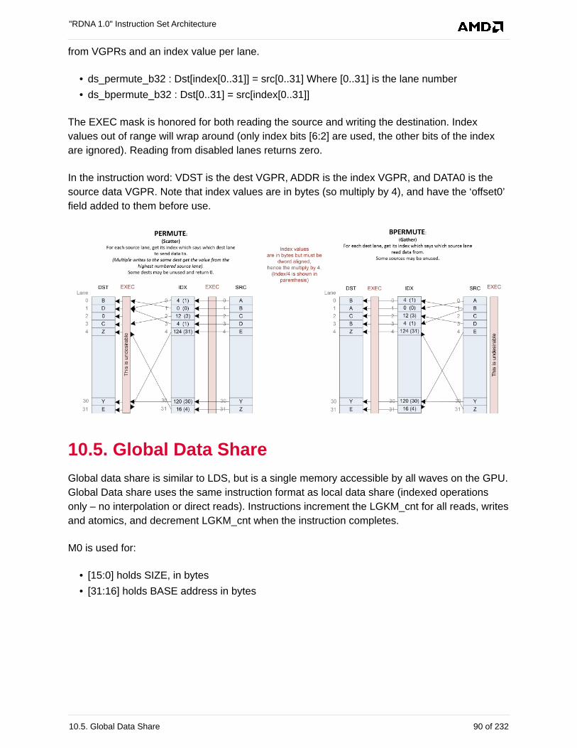
from VGPRs and an index value per lane.
• ds_permute_b32 : Dst[index[0..31]] = src[0..31] Where [0..31] is the lane number
• ds_bpermute_b32 : Dst[0..31] = src[index[0..31]]
The EXEC mask is honored for both reading the source and writing the destination. Index
values out of range will wrap around (only index bits [6:2] are used, the other bits of the index
are ignored). Reading from disabled lanes returns zero.
In the instruction word: VDST is the dest VGPR, ADDR is the index VGPR, and DATA0 is the
source data VGPR. Note that index values are in bytes (so multiply by 4), and have the ‘offset0’
field added to them before use.
10.5. Global Data Share
Global data share is similar to LDS, but is a single memory accessible by all waves on the GPU.
Global Data share uses the same instruction format as local data share (indexed operations
only – no interpolation or direct reads). Instructions increment the LGKM_cnt for all reads, writes
and atomics, and decrement LGKM_cnt when the instruction completes.
M0 is used for:
• [15:0] holds SIZE, in bytes
• [31:16] holds BASE address in bytes
"RDNA 1.0" Instruction Set Architecture
10.5. Global Data Share 90 of 232
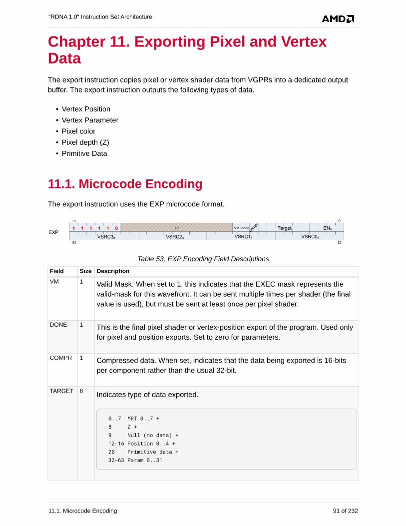
Chapter 11. Exporting Pixel and VertexData
The export instruction copies pixel or vertex shader data from VGPRs into a dedicated output
buffer. The export instruction outputs the following types of data.
• Vertex Position
• Vertex Parameter
• Pixel color
• Pixel depth (Z)
• Primitive Data
11.1. Microcode Encoding
The export instruction uses the EXP microcode format.
Table 53. EXP Encoding Field Descriptions
Field Size Description
VM 1 Valid Mask. When set to 1, this indicates that the EXEC mask represents the
valid-mask for this wavefront. It can be sent multiple times per shader (the final
value is used), but must be sent at least once per pixel shader.
DONE 1 This is the final pixel shader or vertex-position export of the program. Used only
for pixel and position exports. Set to zero for parameters.
COMPR 1 Compressed data. When set, indicates that the data being exported is 16-bits
per component rather than the usual 32-bit.
TARGET 6Indicates type of data exported.
0..7 MRT 0..7 + 8 Z + 9 Null (no data) + 12-16 Position 0..4 + 20 Primitive data + 32-63 Param 0..31
"RDNA 1.0" Instruction Set Architecture
11.1. Microcode Encoding 91 of 232
Field Size Description
EN 4COMPR==1: export half-Dword enable. Valid values are: 0x0,3,C,F.
[0] enables VSRC0 : R,G from one VGPGR
[2] enables VSRC1 : B,A from one VGPR
COMPR==0: [0-3] = enables for VSRC0..3.
EN can be zero (used when exporting only valid mask to NULL target).
VSRC3 8VGPR from which to read data.
Pos & Param: vsrc0=X, 1=Y, 2=Z, 3=W
MRT: vsrc0=R, 1=G, 2=B, 3=A
VSRC2 8
VSRC1 8
VSRC0 8
11.2. Operations
11.2.1. Pixel Shader Exports
Export instructions copy color data to the MRTs. Data has up to four components (R, G, B, A).
Optionally, export instructions also output depth (Z) data.
Every pixel shader must have at least one export instruction. The last export instruction
executed must have the DONE bit set to one.
The EXEC mask is applied to all exports. Only pixels with the corresponding EXEC bit set to 1
export data to the output buffer. Results from multiple exports are accumulated in the output
buffer.
At least one export must have the VM bit set to 1. This export, in addition to copying data to the
color or depth output buffer, also informs the color buffer which pixels are valid and which have
been discarded. The value of the EXEC mask communicates the pixel valid mask. If multiple
exports are sent with VM set to 1, the mask from the final export is used. If the shader program
wants to only update the valid mask but not send any new data, the program can do an export
to the NULL target.
11.2.2. Vertex Shader Exports
The vertex shader uses export instructions to output vertex position data and vertex parameter
data to the output buffer. This data is passed on to subsequent pixel shaders.
Every vertex shader must output at least one position vector (x, y, z; w is optional) to the POS0
target. The last position export must have the DONE bit set to 1. A vertex shader can export
zero or more parameters. For improved performance, it is recommended to output all position
data as early as possible in the vertex shader.
"RDNA 1.0" Instruction Set Architecture
11.2. Operations 92 of 232
11.3. Primitive Shader Exports
The primitive shader may export Position and Primitive data. Before exporting, the shader must
request that space be allocated in the output buffer using the ALLOC_REQ message.
11.4. Dependency Checking
Export instructions are executed by the hardware in two phases. First, the instruction is selected
to be executed, and EXPCNT is incremented by 1. At this time, the hardware requests the use
of internal busses needed to complete the instruction.
When access to the bus is granted, the EXEC mask is read and the VGPR data sent out. After
the last of the VGPR data is sent, the EXPCNT counter is decremented by 1.
Use S_WAITCNT on EXPCNT to prevent the shader program from overwriting EXEC or the
VGPRs holding the data to be exported before the export operation has completed.
Multiple export instructions can be outstanding at one time. Exports of the same type (for
example: position) are completed in order, but exports of different types can be completed out of
order.
If the STATUS register’s SKIP_EXPORT bit is set to one, the hardware treats all EXPORT
instructions as if they were NOPs.
"RDNA 1.0" Instruction Set Architecture
11.3. Primitive Shader Exports 93 of 232
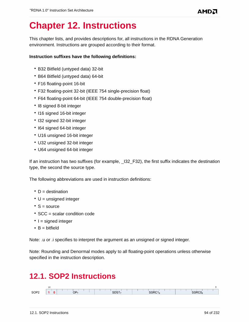
Chapter 12. Instructions
This chapter lists, and provides descriptions for, all instructions in the RDNA Generation
environment. Instructions are grouped according to their format.
Instruction suffixes have the following definitions:
• B32 Bitfield (untyped data) 32-bit
• B64 Bitfield (untyped data) 64-bit
• F16 floating-point 16-bit
• F32 floating-point 32-bit (IEEE 754 single-precision float)
• F64 floating-point 64-bit (IEEE 754 double-precision float)
• I8 signed 8-bit integer
• I16 signed 16-bit integer
• I32 signed 32-bit integer
• I64 signed 64-bit integer
• U16 unsigned 16-bit integer
• U32 unsigned 32-bit integer
• U64 unsigned 64-bit integer
If an instruction has two suffixes (for example, _I32_F32), the first suffix indicates the destination
type, the second the source type.
The following abbreviations are used in instruction definitions:
• D = destination
• U = unsigned integer
• S = source
• SCC = scalar condition code
• I = signed integer
• B = bitfield
Note: .u or .i specifies to interpret the argument as an unsigned or signed integer.
Note: Rounding and Denormal modes apply to all floating-point operations unless otherwise
specified in the instruction description.
12.1. SOP2 Instructions
"RDNA 1.0" Instruction Set Architecture
12.1. SOP2 Instructions 94 of 232
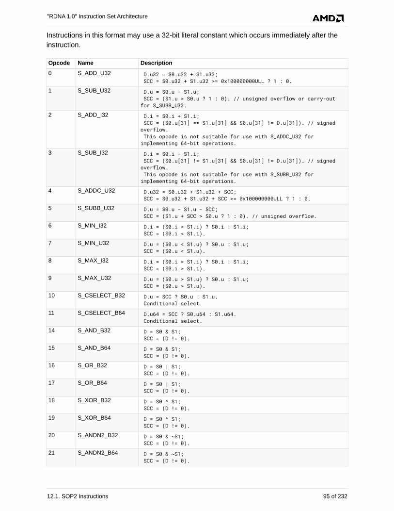
Instructions in this format may use a 32-bit literal constant which occurs immediately after the
instruction.
Opcode Name Description
0 S_ADD_U32 D.u32 = S0.u32 + S1.u32; SCC = S0.u32 + S1.u32 >= 0x100000000ULL ? 1 : 0.
1 S_SUB_U32 D.u = S0.u - S1.u; SCC = (S1.u > S0.u ? 1 : 0). // unsigned overflow or carry-outfor S_SUBB_U32.
2 S_ADD_I32 D.i = S0.i + S1.i; SCC = (S0.u[31] == S1.u[31] && S0.u[31] != D.u[31]). // signedoverflow. This opcode is not suitable for use with S_ADDC_U32 forimplementing 64-bit operations.
3 S_SUB_I32 D.i = S0.i - S1.i; SCC = (S0.u[31] != S1.u[31] && S0.u[31] != D.u[31]). // signedoverflow. This opcode is not suitable for use with S_SUBB_U32 forimplementing 64-bit operations.
4 S_ADDC_U32 D.u32 = S0.u32 + S1.u32 + SCC; SCC = S0.u32 + S1.u32 + SCC >= 0x100000000ULL ? 1 : 0.
5 S_SUBB_U32 D.u = S0.u - S1.u - SCC; SCC = (S1.u + SCC > S0.u ? 1 : 0). // unsigned overflow.
6 S_MIN_I32 D.i = (S0.i < S1.i) ? S0.i : S1.i; SCC = (S0.i < S1.i).
7 S_MIN_U32 D.u = (S0.u < S1.u) ? S0.u : S1.u; SCC = (S0.u < S1.u).
8 S_MAX_I32 D.i = (S0.i > S1.i) ? S0.i : S1.i; SCC = (S0.i > S1.i).
9 S_MAX_U32 D.u = (S0.u > S1.u) ? S0.u : S1.u; SCC = (S0.u > S1.u).
10 S_CSELECT_B32 D.u = SCC ? S0.u : S1.u. Conditional select.
11 S_CSELECT_B64 D.u64 = SCC ? S0.u64 : S1.u64. Conditional select.
14 S_AND_B32 D = S0 & S1; SCC = (D != 0).
15 S_AND_B64 D = S0 & S1; SCC = (D != 0).
16 S_OR_B32 D = S0 | S1; SCC = (D != 0).
17 S_OR_B64 D = S0 | S1; SCC = (D != 0).
18 S_XOR_B32 D = S0 ^ S1; SCC = (D != 0).
19 S_XOR_B64 D = S0 ^ S1; SCC = (D != 0).
20 S_ANDN2_B32 D = S0 & ~S1; SCC = (D != 0).
21 S_ANDN2_B64 D = S0 & ~S1; SCC = (D != 0).
"RDNA 1.0" Instruction Set Architecture
12.1. SOP2 Instructions 95 of 232
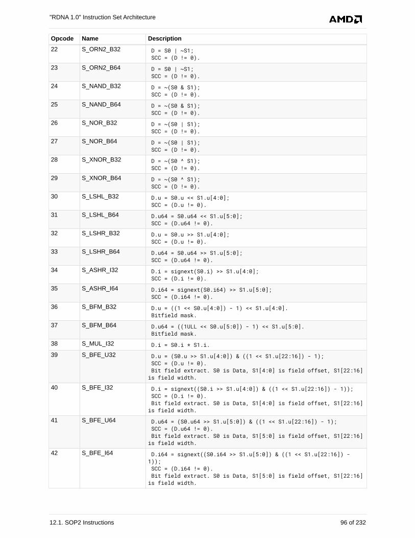
Opcode Name Description
22 S_ORN2_B32 D = S0 | ~S1; SCC = (D != 0).
23 S_ORN2_B64 D = S0 | ~S1; SCC = (D != 0).
24 S_NAND_B32 D = ~(S0 & S1); SCC = (D != 0).
25 S_NAND_B64 D = ~(S0 & S1); SCC = (D != 0).
26 S_NOR_B32 D = ~(S0 | S1); SCC = (D != 0).
27 S_NOR_B64 D = ~(S0 | S1); SCC = (D != 0).
28 S_XNOR_B32 D = ~(S0 ^ S1); SCC = (D != 0).
29 S_XNOR_B64 D = ~(S0 ^ S1); SCC = (D != 0).
30 S_LSHL_B32 D.u = S0.u << S1.u[4:0]; SCC = (D.u != 0).
31 S_LSHL_B64 D.u64 = S0.u64 << S1.u[5:0]; SCC = (D.u64 != 0).
32 S_LSHR_B32 D.u = S0.u >> S1.u[4:0]; SCC = (D.u != 0).
33 S_LSHR_B64 D.u64 = S0.u64 >> S1.u[5:0]; SCC = (D.u64 != 0).
34 S_ASHR_I32 D.i = signext(S0.i) >> S1.u[4:0]; SCC = (D.i != 0).
35 S_ASHR_I64 D.i64 = signext(S0.i64) >> S1.u[5:0]; SCC = (D.i64 != 0).
36 S_BFM_B32 D.u = ((1 << S0.u[4:0]) - 1) << S1.u[4:0]. Bitfield mask.
37 S_BFM_B64 D.u64 = ((1ULL << S0.u[5:0]) - 1) << S1.u[5:0]. Bitfield mask.
38 S_MUL_I32 D.i = S0.i * S1.i.
39 S_BFE_U32 D.u = (S0.u >> S1.u[4:0]) & ((1 << S1.u[22:16]) - 1); SCC = (D.u != 0). Bit field extract. S0 is Data, S1[4:0] is field offset, S1[22:16]is field width.
40 S_BFE_I32 D.i = signext((S0.i >> S1.u[4:0]) & ((1 << S1.u[22:16]) - 1)); SCC = (D.i != 0). Bit field extract. S0 is Data, S1[4:0] is field offset, S1[22:16]is field width.
41 S_BFE_U64 D.u64 = (S0.u64 >> S1.u[5:0]) & ((1 << S1.u[22:16]) - 1); SCC = (D.u64 != 0). Bit field extract. S0 is Data, S1[5:0] is field offset, S1[22:16]is field width.
42 S_BFE_I64 D.i64 = signext((S0.i64 >> S1.u[5:0]) & ((1 << S1.u[22:16]) -1)); SCC = (D.i64 != 0). Bit field extract. S0 is Data, S1[5:0] is field offset, S1[22:16]is field width.
"RDNA 1.0" Instruction Set Architecture
12.1. SOP2 Instructions 96 of 232
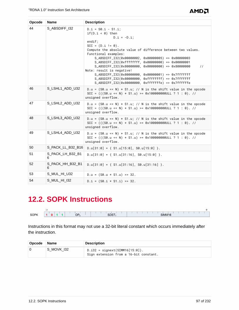
Opcode Name Description
44 S_ABSDIFF_I32 D.i = S0.i - S1.i; if(D.i < 0) then D.i = -D.i; endif; SCC = (D.i != 0). Compute the absolute value of difference between two values. Functional examples: S_ABSDIFF_I32(0x00000002, 0x00000005) => 0x00000003 S_ABSDIFF_I32(0xffffffff, 0x00000000) => 0x00000001 S_ABSDIFF_I32(0x80000000, 0x00000000) => 0x80000000 //Note: result is negative! S_ABSDIFF_I32(0x80000000, 0x00000001) => 0x7fffffff S_ABSDIFF_I32(0x80000000, 0xffffffff) => 0x7fffffff S_ABSDIFF_I32(0x80000000, 0xfffffffe) => 0x7ffffffe
46 S_LSHL1_ADD_U32 D.u = (S0.u << N) + S1.u; // N is the shift value in the opcode SCC = (((S0.u << N) + S1.u) >= 0x100000000ULL ? 1 : 0). //unsigned overflow.
47 S_LSHL2_ADD_U32 D.u = (S0.u << N) + S1.u; // N is the shift value in the opcode SCC = (((S0.u << N) + S1.u) >= 0x100000000ULL ? 1 : 0). //unsigned overflow.
48 S_LSHL3_ADD_U32 D.u = (S0.u << N) + S1.u; // N is the shift value in the opcode SCC = (((S0.u << N) + S1.u) >= 0x100000000ULL ? 1 : 0). //unsigned overflow.
49 S_LSHL4_ADD_U32 D.u = (S0.u << N) + S1.u; // N is the shift value in the opcode SCC = (((S0.u << N) + S1.u) >= 0x100000000ULL ? 1 : 0). //unsigned overflow.
50 S_PACK_LL_B32_B16 D.u[31:0] = { S1.u[15:0], S0.u[15:0] }.
51 S_PACK_LH_B32_B16
D.u[31:0] = { S1.u[31:16], S0.u[15:0] }.
52 S_PACK_HH_B32_B16
D.u[31:0] = { S1.u[31:16], S0.u[31:16] }.
53 S_MUL_HI_U32 D.u = (S0.u * S1.u) >> 32.
54 S_MUL_HI_I32 D.i = (S0.i * S1.i) >> 32.
12.2. SOPK Instructions
Instructions in this format may not use a 32-bit literal constant which occurs immediately after
the instruction.
Opcode Name Description
0 S_MOVK_I32 D.i32 = signext(SIMM16[15:0]). Sign extension from a 16-bit constant.
"RDNA 1.0" Instruction Set Architecture
12.2. SOPK Instructions 97 of 232
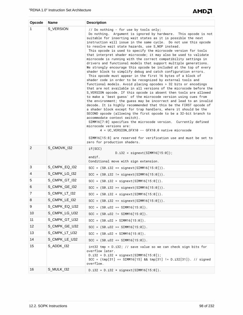
Opcode Name Description
1 S_VERSION // Do nothing - for use by tools only; Do nothing. Argument is ignored by hardware. This opcode is notsuitable for inserting wait states as it is possible the nextinstruction will issue in the same cycle. Do not use this opcodeto resolve wait state hazards, use S_NOP instead. This opcode is used to specify the microcode version for toolsthat interpret shader microcode; it may also be used to validatemicrocode is running with the correct compatibility settings indrivers and functional models that support multiple generations.We strongly encourage this opcode be included at the top of everyshader block to simplify debug and catch configuration errors. This opcode must appear in the first 16 bytes of a block ofshader code in order to be recognized by external tools andfunctional models. Avoid placing opcodes > 32 bits or encodingsthat are not available in all versions of the microcode before theS_VERSION opcode. If this opcode is absent then tools are allowedto make a 'best guess' of the microcode version using cues fromthe environment; the guess may be incorrect and lead to an invaliddecode. It is highly recommended that this be the FIRST opcode ofa shader block except for trap handlers, where it should be theSECOND opcode (allowing the first opcode to be a 32-bit branch toaccommodate context switch). SIMM16[7:0] specifies the microcode version. Currently definedmicrocode versions are: 4 = UC_VERSION_GFX10 -- GFX10.0 native microcode
SIMM16[15:8] are reserved for verification use and must be set tozero for production shaders.
2 S_CMOVK_I32 if(SCC) D.i32 = signext(SIMM16[15:0]); endif. Conditional move with sign extension.
3 S_CMPK_EQ_I32 SCC = (S0.i32 == signext(SIMM16[15:0])).
4 S_CMPK_LG_I32 SCC = (S0.i32 != signext(SIMM16[15:0])).
5 S_CMPK_GT_I32 SCC = (S0.i32 > signext(SIMM16[15:0])).
6 S_CMPK_GE_I32 SCC = (S0.i32 >= signext(SIMM16[15:0])).
7 S_CMPK_LT_I32 SCC = (S0.i32 < signext(SIMM16[15:0])).
8 S_CMPK_LE_I32 SCC = (S0.i32 <= signext(SIMM16[15:0])).
9 S_CMPK_EQ_U32 SCC = (S0.u32 == SIMM16[15:0]).
10 S_CMPK_LG_U32 SCC = (S0.u32 != SIMM16[15:0]).
11 S_CMPK_GT_U32 SCC = (S0.u32 > SIMM16[15:0]).
12 S_CMPK_GE_U32 SCC = (S0.u32 >= SIMM16[15:0]).
13 S_CMPK_LT_U32 SCC = (S0.u32 < SIMM16[15:0]).
14 S_CMPK_LE_U32 SCC = (S0.u32 <= SIMM16[15:0]).
15 S_ADDK_I32 int32 tmp = D.i32; // save value so we can check sign bits foroverflow later. D.i32 = D.i32 + signext(SIMM16[15:0]); SCC = (tmp[31] == SIMM16[15] && tmp[31] != D.i32[31]). // signedoverflow.
16 S_MULK_I32 D.i32 = D.i32 * signext(SIMM16[15:0]).
"RDNA 1.0" Instruction Set Architecture
12.2. SOPK Instructions 98 of 232
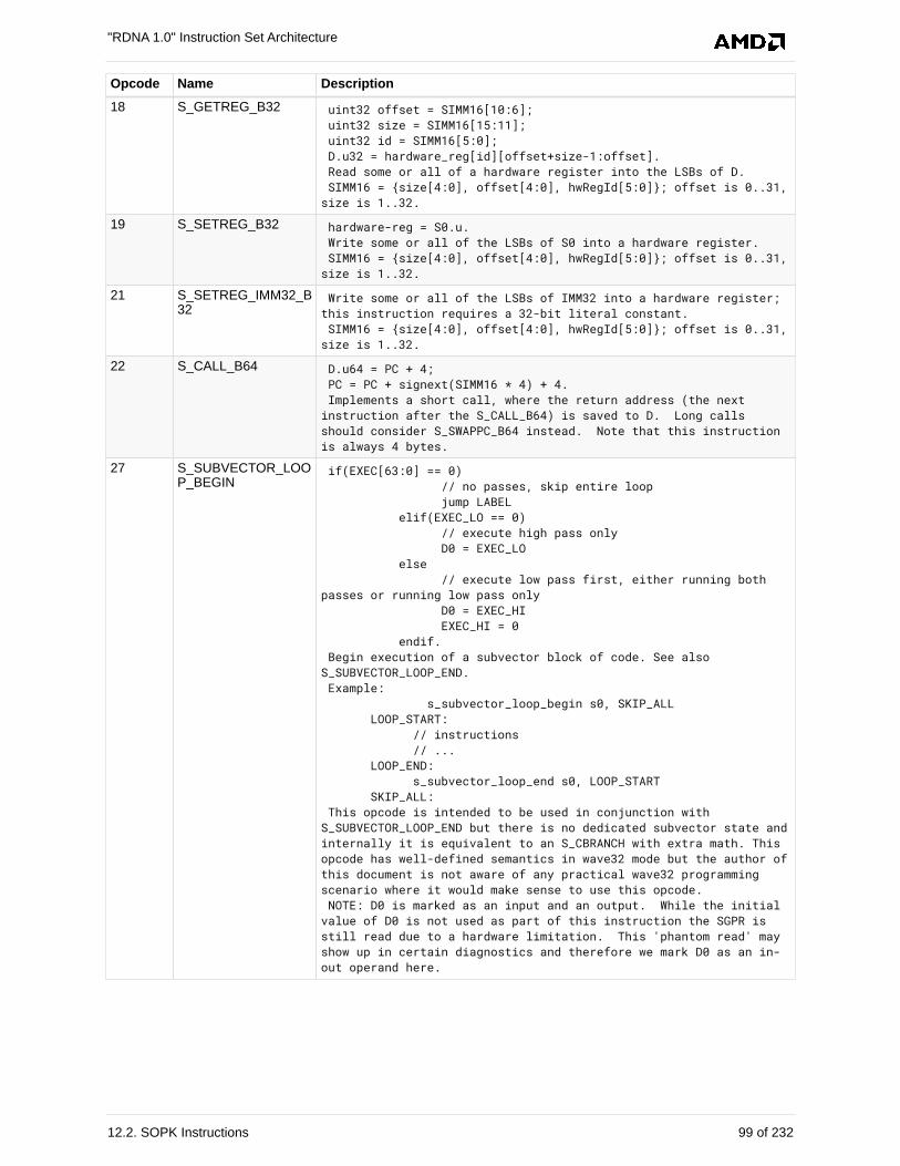
Opcode Name Description
18 S_GETREG_B32 uint32 offset = SIMM16[10:6]; uint32 size = SIMM16[15:11]; uint32 id = SIMM16[5:0]; D.u32 = hardware_reg[id][offset+size-1:offset]. Read some or all of a hardware register into the LSBs of D. SIMM16 = {size[4:0], offset[4:0], hwRegId[5:0]}; offset is 0..31,size is 1..32.
19 S_SETREG_B32 hardware-reg = S0.u. Write some or all of the LSBs of S0 into a hardware register. SIMM16 = {size[4:0], offset[4:0], hwRegId[5:0]}; offset is 0..31,size is 1..32.
21 S_SETREG_IMM32_B32
Write some or all of the LSBs of IMM32 into a hardware register;this instruction requires a 32-bit literal constant. SIMM16 = {size[4:0], offset[4:0], hwRegId[5:0]}; offset is 0..31,size is 1..32.
22 S_CALL_B64 D.u64 = PC + 4; PC = PC + signext(SIMM16 * 4) + 4. Implements a short call, where the return address (the nextinstruction after the S_CALL_B64) is saved to D. Long callsshould consider S_SWAPPC_B64 instead. Note that this instructionis always 4 bytes.
27 S_SUBVECTOR_LOOP_BEGIN
if(EXEC[63:0] == 0) // no passes, skip entire loop jump LABEL elif(EXEC_LO == 0) // execute high pass only D0 = EXEC_LO else // execute low pass first, either running bothpasses or running low pass only D0 = EXEC_HI EXEC_HI = 0 endif. Begin execution of a subvector block of code. See alsoS_SUBVECTOR_LOOP_END. Example: s_subvector_loop_begin s0, SKIP_ALL LOOP_START: // instructions // ... LOOP_END: s_subvector_loop_end s0, LOOP_START SKIP_ALL: This opcode is intended to be used in conjunction withS_SUBVECTOR_LOOP_END but there is no dedicated subvector state andinternally it is equivalent to an S_CBRANCH with extra math. Thisopcode has well-defined semantics in wave32 mode but the author ofthis document is not aware of any practical wave32 programmingscenario where it would make sense to use this opcode. NOTE: D0 is marked as an input and an output. While the initialvalue of D0 is not used as part of this instruction the SGPR isstill read due to a hardware limitation. This 'phantom read' mayshow up in certain diagnostics and therefore we mark D0 as an in-out operand here.
"RDNA 1.0" Instruction Set Architecture
12.2. SOPK Instructions 99 of 232
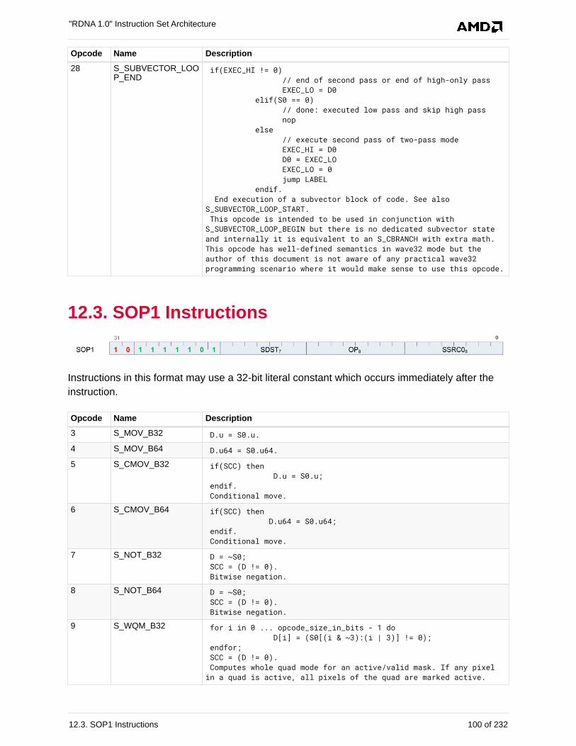
Opcode Name Description
28 S_SUBVECTOR_LOOP_END
if(EXEC_HI != 0) // end of second pass or end of high-only pass EXEC_LO = D0 elif(S0 == 0) // done: executed low pass and skip high pass nop else // execute second pass of two-pass mode EXEC_HI = D0 D0 = EXEC_LO EXEC_LO = 0 jump LABEL endif. End execution of a subvector block of code. See alsoS_SUBVECTOR_LOOP_START. This opcode is intended to be used in conjunction withS_SUBVECTOR_LOOP_BEGIN but there is no dedicated subvector stateand internally it is equivalent to an S_CBRANCH with extra math.This opcode has well-defined semantics in wave32 mode but theauthor of this document is not aware of any practical wave32programming scenario where it would make sense to use this opcode.
12.3. SOP1 Instructions
Instructions in this format may use a 32-bit literal constant which occurs immediately after the
instruction.
Opcode Name Description
3 S_MOV_B32 D.u = S0.u.
4 S_MOV_B64 D.u64 = S0.u64.
5 S_CMOV_B32 if(SCC) then D.u = S0.u; endif. Conditional move.
6 S_CMOV_B64 if(SCC) then D.u64 = S0.u64; endif. Conditional move.
7 S_NOT_B32 D = ~S0; SCC = (D != 0). Bitwise negation.
8 S_NOT_B64 D = ~S0; SCC = (D != 0). Bitwise negation.
9 S_WQM_B32 for i in 0 ... opcode_size_in_bits - 1 do D[i] = (S0[(i & ~3):(i | 3)] != 0); endfor; SCC = (D != 0). Computes whole quad mode for an active/valid mask. If any pixelin a quad is active, all pixels of the quad are marked active.
"RDNA 1.0" Instruction Set Architecture
12.3. SOP1 Instructions 100 of 232
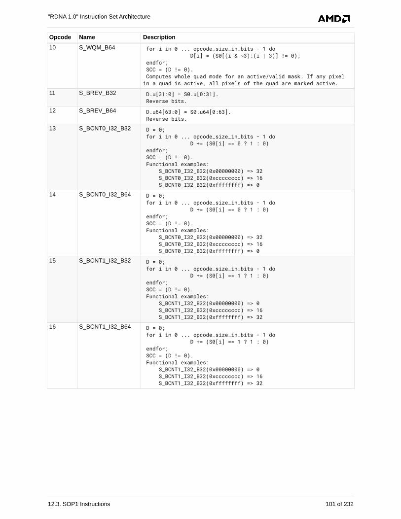
Opcode Name Description
10 S_WQM_B64 for i in 0 ... opcode_size_in_bits - 1 do D[i] = (S0[(i & ~3):(i | 3)] != 0); endfor; SCC = (D != 0). Computes whole quad mode for an active/valid mask. If any pixelin a quad is active, all pixels of the quad are marked active.
11 S_BREV_B32 D.u[31:0] = S0.u[0:31]. Reverse bits.
12 S_BREV_B64 D.u64[63:0] = S0.u64[0:63]. Reverse bits.
13 S_BCNT0_I32_B32 D = 0; for i in 0 ... opcode_size_in_bits - 1 do D += (S0[i] == 0 ? 1 : 0) endfor; SCC = (D != 0). Functional examples: S_BCNT0_I32_B32(0x00000000) => 32 S_BCNT0_I32_B32(0xcccccccc) => 16 S_BCNT0_I32_B32(0xffffffff) => 0
14 S_BCNT0_I32_B64 D = 0; for i in 0 ... opcode_size_in_bits - 1 do D += (S0[i] == 0 ? 1 : 0) endfor; SCC = (D != 0). Functional examples: S_BCNT0_I32_B32(0x00000000) => 32 S_BCNT0_I32_B32(0xcccccccc) => 16 S_BCNT0_I32_B32(0xffffffff) => 0
15 S_BCNT1_I32_B32 D = 0; for i in 0 ... opcode_size_in_bits - 1 do D += (S0[i] == 1 ? 1 : 0) endfor; SCC = (D != 0). Functional examples: S_BCNT1_I32_B32(0x00000000) => 0 S_BCNT1_I32_B32(0xcccccccc) => 16 S_BCNT1_I32_B32(0xffffffff) => 32
16 S_BCNT1_I32_B64 D = 0; for i in 0 ... opcode_size_in_bits - 1 do D += (S0[i] == 1 ? 1 : 0) endfor; SCC = (D != 0). Functional examples: S_BCNT1_I32_B32(0x00000000) => 0 S_BCNT1_I32_B32(0xcccccccc) => 16 S_BCNT1_I32_B32(0xffffffff) => 32
"RDNA 1.0" Instruction Set Architecture
12.3. SOP1 Instructions 101 of 232
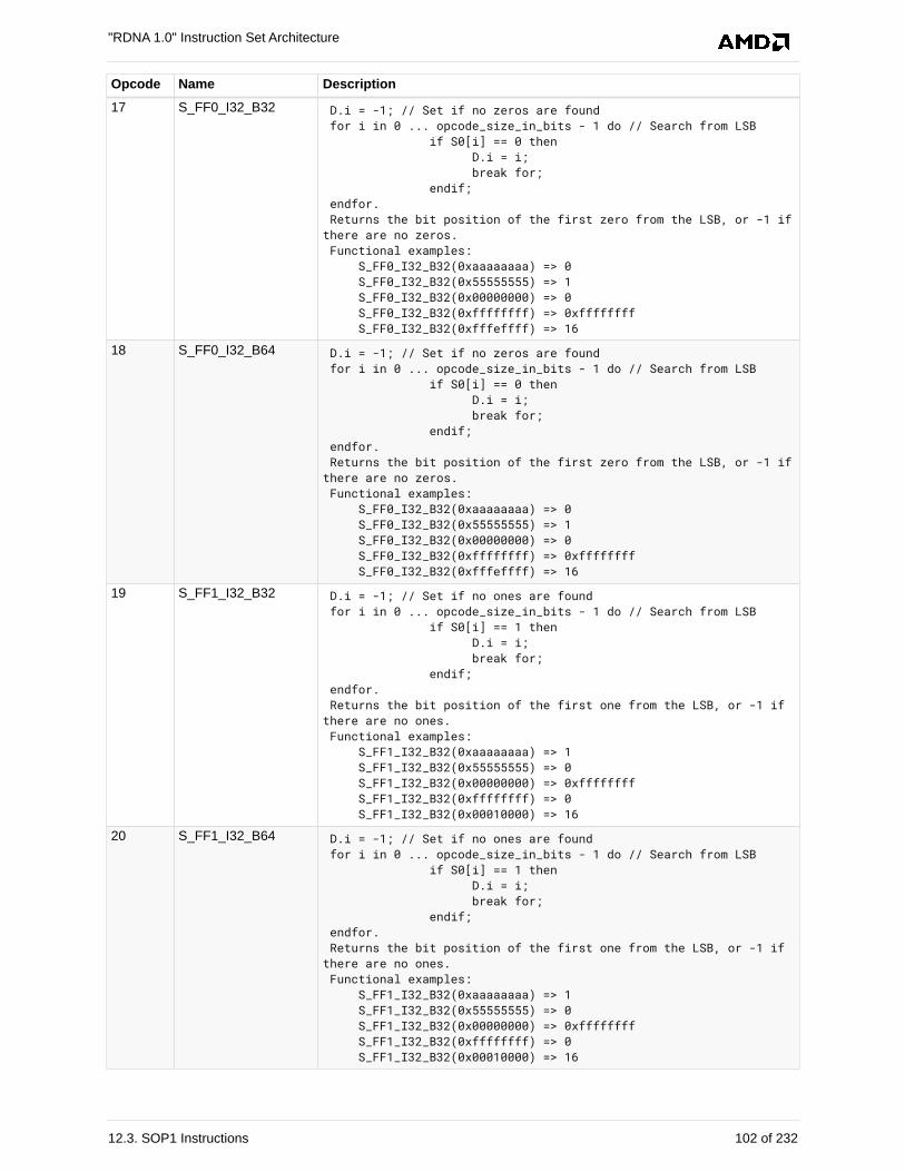
Opcode Name Description
17 S_FF0_I32_B32 D.i = -1; // Set if no zeros are found for i in 0 ... opcode_size_in_bits - 1 do // Search from LSB if S0[i] == 0 then D.i = i; break for; endif; endfor. Returns the bit position of the first zero from the LSB, or -1 ifthere are no zeros. Functional examples: S_FF0_I32_B32(0xaaaaaaaa) => 0 S_FF0_I32_B32(0x55555555) => 1 S_FF0_I32_B32(0x00000000) => 0 S_FF0_I32_B32(0xffffffff) => 0xffffffff S_FF0_I32_B32(0xfffeffff) => 16
18 S_FF0_I32_B64 D.i = -1; // Set if no zeros are found for i in 0 ... opcode_size_in_bits - 1 do // Search from LSB if S0[i] == 0 then D.i = i; break for; endif; endfor. Returns the bit position of the first zero from the LSB, or -1 ifthere are no zeros. Functional examples: S_FF0_I32_B32(0xaaaaaaaa) => 0 S_FF0_I32_B32(0x55555555) => 1 S_FF0_I32_B32(0x00000000) => 0 S_FF0_I32_B32(0xffffffff) => 0xffffffff S_FF0_I32_B32(0xfffeffff) => 16
19 S_FF1_I32_B32 D.i = -1; // Set if no ones are found for i in 0 ... opcode_size_in_bits - 1 do // Search from LSB if S0[i] == 1 then D.i = i; break for; endif; endfor. Returns the bit position of the first one from the LSB, or -1 ifthere are no ones. Functional examples: S_FF1_I32_B32(0xaaaaaaaa) => 1 S_FF1_I32_B32(0x55555555) => 0 S_FF1_I32_B32(0x00000000) => 0xffffffff S_FF1_I32_B32(0xffffffff) => 0 S_FF1_I32_B32(0x00010000) => 16
20 S_FF1_I32_B64 D.i = -1; // Set if no ones are found for i in 0 ... opcode_size_in_bits - 1 do // Search from LSB if S0[i] == 1 then D.i = i; break for; endif; endfor. Returns the bit position of the first one from the LSB, or -1 ifthere are no ones. Functional examples: S_FF1_I32_B32(0xaaaaaaaa) => 1 S_FF1_I32_B32(0x55555555) => 0 S_FF1_I32_B32(0x00000000) => 0xffffffff S_FF1_I32_B32(0xffffffff) => 0 S_FF1_I32_B32(0x00010000) => 16
"RDNA 1.0" Instruction Set Architecture
12.3. SOP1 Instructions 102 of 232
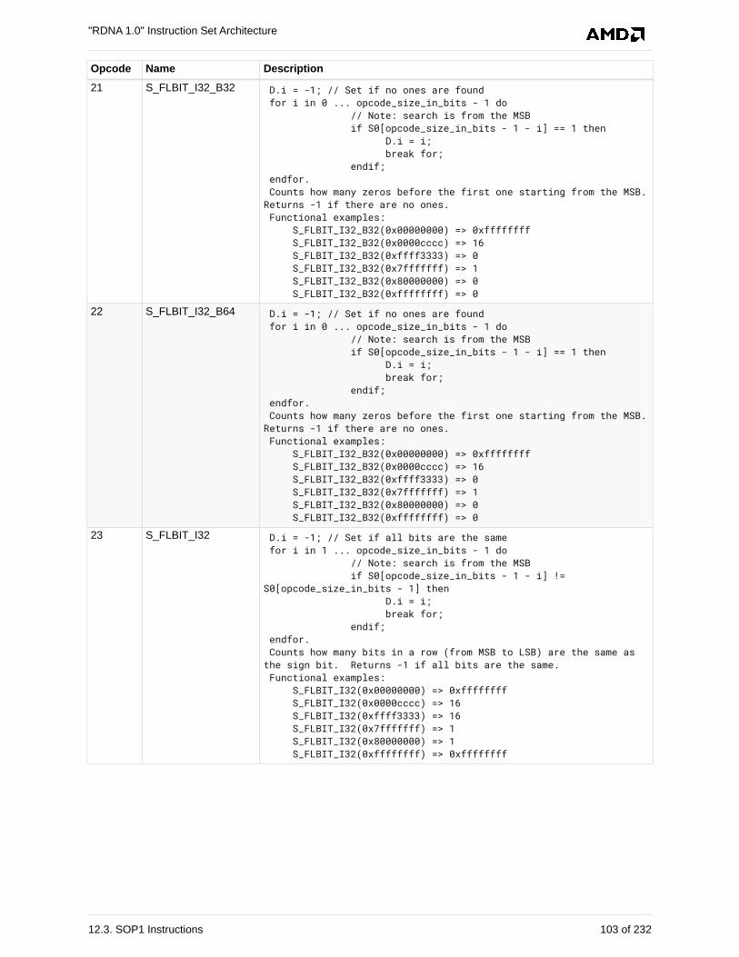
Opcode Name Description
21 S_FLBIT_I32_B32 D.i = -1; // Set if no ones are found for i in 0 ... opcode_size_in_bits - 1 do // Note: search is from the MSB if S0[opcode_size_in_bits - 1 - i] == 1 then D.i = i; break for; endif; endfor. Counts how many zeros before the first one starting from the MSB.Returns -1 if there are no ones. Functional examples: S_FLBIT_I32_B32(0x00000000) => 0xffffffff S_FLBIT_I32_B32(0x0000cccc) => 16 S_FLBIT_I32_B32(0xffff3333) => 0 S_FLBIT_I32_B32(0x7fffffff) => 1 S_FLBIT_I32_B32(0x80000000) => 0 S_FLBIT_I32_B32(0xffffffff) => 0
22 S_FLBIT_I32_B64 D.i = -1; // Set if no ones are found for i in 0 ... opcode_size_in_bits - 1 do // Note: search is from the MSB if S0[opcode_size_in_bits - 1 - i] == 1 then D.i = i; break for; endif; endfor. Counts how many zeros before the first one starting from the MSB.Returns -1 if there are no ones. Functional examples: S_FLBIT_I32_B32(0x00000000) => 0xffffffff S_FLBIT_I32_B32(0x0000cccc) => 16 S_FLBIT_I32_B32(0xffff3333) => 0 S_FLBIT_I32_B32(0x7fffffff) => 1 S_FLBIT_I32_B32(0x80000000) => 0 S_FLBIT_I32_B32(0xffffffff) => 0
23 S_FLBIT_I32 D.i = -1; // Set if all bits are the same for i in 1 ... opcode_size_in_bits - 1 do // Note: search is from the MSB if S0[opcode_size_in_bits - 1 - i] !=S0[opcode_size_in_bits - 1] then D.i = i; break for; endif; endfor. Counts how many bits in a row (from MSB to LSB) are the same asthe sign bit. Returns -1 if all bits are the same. Functional examples: S_FLBIT_I32(0x00000000) => 0xffffffff S_FLBIT_I32(0x0000cccc) => 16 S_FLBIT_I32(0xffff3333) => 16 S_FLBIT_I32(0x7fffffff) => 1 S_FLBIT_I32(0x80000000) => 1 S_FLBIT_I32(0xffffffff) => 0xffffffff
"RDNA 1.0" Instruction Set Architecture
12.3. SOP1 Instructions 103 of 232
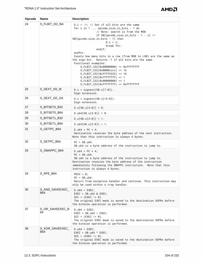
Opcode Name Description
24 S_FLBIT_I32_I64 D.i = -1; // Set if all bits are the same for i in 1 ... opcode_size_in_bits - 1 do // Note: search is from the MSB if S0[opcode_size_in_bits - 1 - i] !=S0[opcode_size_in_bits - 1] then D.i = i; break for; endif; endfor. Counts how many bits in a row (from MSB to LSB) are the same asthe sign bit. Returns -1 if all bits are the same. Functional examples: S_FLBIT_I32(0x00000000) => 0xffffffff S_FLBIT_I32(0x0000cccc) => 16 S_FLBIT_I32(0xffff3333) => 16 S_FLBIT_I32(0x7fffffff) => 1 S_FLBIT_I32(0x80000000) => 1 S_FLBIT_I32(0xffffffff) => 0xffffffff
25 S_SEXT_I32_I8 D.i = signext(S0.i[7:0]). Sign extension.
26 S_SEXT_I32_I16 D.i = signext(S0.i[15:0]). Sign extension.
27 S_BITSET0_B32 D.u[S0.u[4:0]] = 0.
28 S_BITSET0_B64 D.u64[S0.u[5:0]] = 0.
29 S_BITSET1_B32 D.u[S0.u[4:0]] = 1.
30 S_BITSET1_B64 D.u64[S0.u[5:0]] = 1.
31 S_GETPC_B64 D.u64 = PC + 4. Destination receives the byte address of the next instruction.Note that this instruction is always 4 bytes.
32 S_SETPC_B64 PC = S0.u64. S0.u64 is a byte address of the instruction to jump to.
33 S_SWAPPC_B64 D.u64 = PC + 4; PC = S0.u64. S0.u64 is a byte address of the instruction to jump to.Destination receives the byte address of the instructionimmediately following the SWAPPC instruction. Note that thisinstruction is always 4 bytes.
34 S_RFE_B64 PRIV = 0; PC = S0.u64. Return from exception handler and continue. This instruction mayonly be used within a trap handler.
36 S_AND_SAVEEXEC_B64
D.u64 = EXEC; EXEC = S0.u64 & EXEC; SCC = (EXEC != 0). The original EXEC mask is saved to the destination SGPRs beforethe bitwise operation is performed.
37 S_OR_SAVEEXEC_B64
D.u64 = EXEC; EXEC = S0.u64 | EXEC; SCC = (EXEC != 0). The original EXEC mask is saved to the destination SGPRs beforethe bitwise operation is performed.
38 S_XOR_SAVEEXEC_B64
D.u64 = EXEC; EXEC = S0.u64 ^ EXEC; SCC = (EXEC != 0). The original EXEC mask is saved to the destination SGPRs beforethe bitwise operation is performed.
"RDNA 1.0" Instruction Set Architecture
12.3. SOP1 Instructions 104 of 232
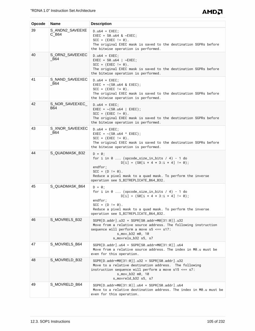
Opcode Name Description
39 S_ANDN2_SAVEEXEC_B64
D.u64 = EXEC; EXEC = S0.u64 & ~EXEC; SCC = (EXEC != 0). The original EXEC mask is saved to the destination SGPRs beforethe bitwise operation is performed.
40 S_ORN2_SAVEEXEC_B64
D.u64 = EXEC; EXEC = S0.u64 | ~EXEC; SCC = (EXEC != 0). The original EXEC mask is saved to the destination SGPRs beforethe bitwise operation is performed.
41 S_NAND_SAVEEXEC_B64
D.u64 = EXEC; EXEC = ~(S0.u64 & EXEC); SCC = (EXEC != 0). The original EXEC mask is saved to the destination SGPRs beforethe bitwise operation is performed.
42 S_NOR_SAVEEXEC_B64
D.u64 = EXEC; EXEC = ~(S0.u64 | EXEC); SCC = (EXEC != 0). The original EXEC mask is saved to the destination SGPRs beforethe bitwise operation is performed.
43 S_XNOR_SAVEEXEC_B64
D.u64 = EXEC; EXEC = ~(S0.u64 ^ EXEC); SCC = (EXEC != 0). The original EXEC mask is saved to the destination SGPRs beforethe bitwise operation is performed.
44 S_QUADMASK_B32 D = 0; for i in 0 ... (opcode_size_in_bits / 4) - 1 do D[i] = (S0[i * 4 + 3:i * 4] != 0); endfor; SCC = (D != 0). Reduce a pixel mask to a quad mask. To perform the inverseoperation see S_BITREPLICATE_B64_B32.
45 S_QUADMASK_B64 D = 0; for i in 0 ... (opcode_size_in_bits / 4) - 1 do D[i] = (S0[i * 4 + 3:i * 4] != 0); endfor; SCC = (D != 0). Reduce a pixel mask to a quad mask. To perform the inverseoperation see S_BITREPLICATE_B64_B32.
46 S_MOVRELS_B32 SGPR[D.addr].u32 = SGPR[S0.addr+M0[31:0]].u32 Move from a relative source address. The following instructionsequence will perform a move s5 <== s17: s_mov_b32 m0, 10 s_movrels_b32 s5, s7
47 S_MOVRELS_B64 SGPR[D.addr].u64 = SGPR[S0.addr+M0[31:0]].u64 Move from a relative source address. The index in M0.u must beeven for this operation.
48 S_MOVRELD_B32 SGPR[D.addr+M0[31:0]].u32 = SGPR[S0.addr].u32 Move to a relative destination address. The followinginstruction sequence will perform a move s15 <== s7: s_mov_b32 m0, 10 s_movreld_b32 s5, s7
49 S_MOVRELD_B64 SGPR[D.addr+M0[31:0]].u64 = SGPR[S0.addr].u64 Move to a relative destination address. The index in M0.u must beeven for this operation.
"RDNA 1.0" Instruction Set Architecture
12.3. SOP1 Instructions 105 of 232
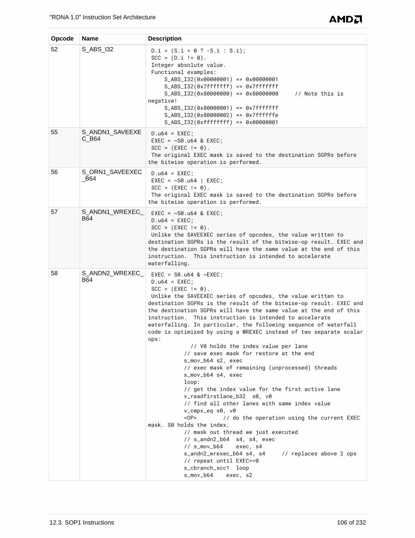
Opcode Name Description
52 S_ABS_I32 D.i = (S.i < 0 ? -S.i : S.i); SCC = (D.i != 0). Integer absolute value. Functional examples: S_ABS_I32(0x00000001) => 0x00000001 S_ABS_I32(0x7fffffff) => 0x7fffffff S_ABS_I32(0x80000000) => 0x80000000 // Note this isnegative! S_ABS_I32(0x80000001) => 0x7fffffff S_ABS_I32(0x80000002) => 0x7ffffffe S_ABS_I32(0xffffffff) => 0x00000001
55 S_ANDN1_SAVEEXEC_B64
D.u64 = EXEC; EXEC = ~S0.u64 & EXEC; SCC = (EXEC != 0). The original EXEC mask is saved to the destination SGPRs beforethe bitwise operation is performed.
56 S_ORN1_SAVEEXEC_B64
D.u64 = EXEC; EXEC = ~S0.u64 | EXEC; SCC = (EXEC != 0). The original EXEC mask is saved to the destination SGPRs beforethe bitwise operation is performed.
57 S_ANDN1_WREXEC_B64
EXEC = ~S0.u64 & EXEC; D.u64 = EXEC; SCC = (EXEC != 0). Unlike the SAVEEXEC series of opcodes, the value written todestination SGPRs is the result of the bitwise-op result. EXEC andthe destination SGPRs will have the same value at the end of thisinstruction. This instruction is intended to acceleratewaterfalling.
58 S_ANDN2_WREXEC_B64
EXEC = S0.u64 & ~EXEC; D.u64 = EXEC; SCC = (EXEC != 0). Unlike the SAVEEXEC series of opcodes, the value written todestination SGPRs is the result of the bitwise-op result. EXEC andthe destination SGPRs will have the same value at the end of thisinstruction. This instruction is intended to acceleratewaterfalling. In particular, the following sequence of waterfallcode is optimized by using a WREXEC instead of two separate scalarops: // V0 holds the index value per lane // save exec mask for restore at the end s_mov_b64 s2, exec // exec mask of remaining (unprocessed) threads s_mov_b64 s4, exec loop: // get the index value for the first active lane v_readfirstlane_b32 s0, v0 // find all other lanes with same index value v_cmpx_eq s0, v0 <OP> // do the operation using the current EXECmask. S0 holds the index. // mask out thread we just executed // s_andn2_b64 s4, s4, exec // s_mov_b64 exec, s4 s_andn2_wrexec_b64 s4, s4 // replaces above 2 ops // repeat until EXEC==0 s_cbranch_scc1 loop s_mov_b64 exec, s2
"RDNA 1.0" Instruction Set Architecture
12.3. SOP1 Instructions 106 of 232
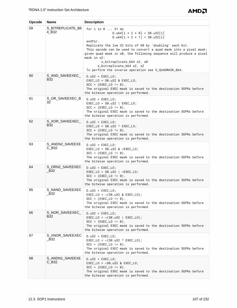
Opcode Name Description
59 S_BITREPLICATE_B64_B32
for i in 0 ... 31 do D.u64[i * 2 + 0] = S0.u32[i] D.u64[i * 2 + 1] = S0.u32[i] endfor. Replicate the low 32 bits of S0 by 'doubling' each bit. This opcode can be used to convert a quad mask into a pixel mask;given quad mask in s0, the following sequence will produce a pixelmask in s2: s_bitreplicate_b64 s2, s0 s_bitreplicate_b64 s2, s2 To perform the inverse operation see S_QUADMASK_B64.
60 S_AND_SAVEEXEC_B32
D.u32 = EXEC_LO; EXEC_LO = S0.u32 & EXEC_LO; SCC = (EXEC_LO != 0). The original EXEC mask is saved to the destination SGPRs beforethe bitwise operation is performed.
61 S_OR_SAVEEXEC_B32
D.u32 = EXEC_LO; EXEC_LO = S0.u32 | EXEC_LO; SCC = (EXEC_LO != 0). The original EXEC mask is saved to the destination SGPRs beforethe bitwise operation is performed.
62 S_XOR_SAVEEXEC_B32
D.u32 = EXEC_LO; EXEC_LO = S0.u32 ^ EXEC_LO; SCC = (EXEC_LO != 0). The original EXEC mask is saved to the destination SGPRs beforethe bitwise operation is performed.
63 S_ANDN2_SAVEEXEC_B32
D.u32 = EXEC_LO; EXEC_LO = S0.u32 & ~EXEC_LO; SCC = (EXEC_LO != 0). The original EXEC mask is saved to the destination SGPRs beforethe bitwise operation is performed.
64 S_ORN2_SAVEEXEC_B32
D.u32 = EXEC_LO; EXEC_LO = S0.u32 | ~EXEC_LO; SCC = (EXEC_LO != 0). The original EXEC mask is saved to the destination SGPRs beforethe bitwise operation is performed.
65 S_NAND_SAVEEXEC_B32
D.u32 = EXEC_LO; EXEC_LO = ~(S0.u32 & EXEC_LO); SCC = (EXEC_LO != 0). The original EXEC mask is saved to the destination SGPRs beforethe bitwise operation is performed.
66 S_NOR_SAVEEXEC_B32
D.u32 = EXEC_LO; EXEC_LO = ~(S0.u32 | EXEC_LO); SCC = (EXEC_LO != 0). The original EXEC mask is saved to the destination SGPRs beforethe bitwise operation is performed.
67 S_XNOR_SAVEEXEC_B32
D.u32 = EXEC_LO; EXEC_LO = ~(S0.u32 ^ EXEC_LO); SCC = (EXEC_LO != 0). The original EXEC mask is saved to the destination SGPRs beforethe bitwise operation is performed.
68 S_ANDN1_SAVEEXEC_B32
D.u32 = EXEC_LO; EXEC_LO = ~S0.u32 & EXEC_LO; SCC = (EXEC_LO != 0). The original EXEC mask is saved to the destination SGPRs beforethe bitwise operation is performed.
"RDNA 1.0" Instruction Set Architecture
12.3. SOP1 Instructions 107 of 232
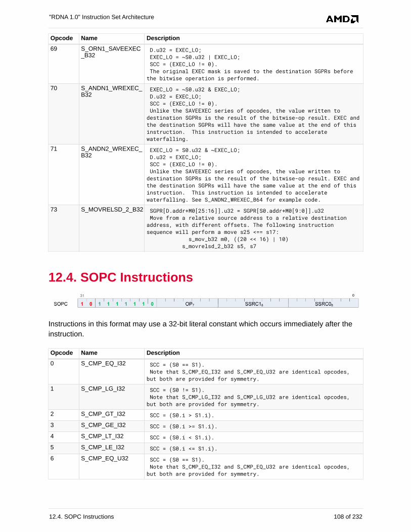
Opcode Name Description
69 S_ORN1_SAVEEXEC_B32
D.u32 = EXEC_LO; EXEC_LO = ~S0.u32 | EXEC_LO; SCC = (EXEC_LO != 0). The original EXEC mask is saved to the destination SGPRs beforethe bitwise operation is performed.
70 S_ANDN1_WREXEC_B32
EXEC_LO = ~S0.u32 & EXEC_LO; D.u32 = EXEC_LO; SCC = (EXEC_LO != 0). Unlike the SAVEEXEC series of opcodes, the value written todestination SGPRs is the result of the bitwise-op result. EXEC andthe destination SGPRs will have the same value at the end of thisinstruction. This instruction is intended to acceleratewaterfalling.
71 S_ANDN2_WREXEC_B32
EXEC_LO = S0.u32 & ~EXEC_LO; D.u32 = EXEC_LO; SCC = (EXEC_LO != 0). Unlike the SAVEEXEC series of opcodes, the value written todestination SGPRs is the result of the bitwise-op result. EXEC andthe destination SGPRs will have the same value at the end of thisinstruction. This instruction is intended to acceleratewaterfalling. See S_ANDN2_WREXEC_B64 for example code.
73 S_MOVRELSD_2_B32 SGPR[D.addr+M0[25:16]].u32 = SGPR[S0.addr+M0[9:0]].u32 Move from a relative source address to a relative destinationaddress, with different offsets. The following instructionsequence will perform a move s25 <== s17: s_mov_b32 m0, ((20 << 16) | 10) s_movrelsd_2_b32 s5, s7
12.4. SOPC Instructions
Instructions in this format may use a 32-bit literal constant which occurs immediately after the
instruction.
Opcode Name Description
0 S_CMP_EQ_I32 SCC = (S0 == S1). Note that S_CMP_EQ_I32 and S_CMP_EQ_U32 are identical opcodes,but both are provided for symmetry.
1 S_CMP_LG_I32 SCC = (S0 != S1). Note that S_CMP_LG_I32 and S_CMP_LG_U32 are identical opcodes,but both are provided for symmetry.
2 S_CMP_GT_I32 SCC = (S0.i > S1.i).
3 S_CMP_GE_I32 SCC = (S0.i >= S1.i).
4 S_CMP_LT_I32 SCC = (S0.i < S1.i).
5 S_CMP_LE_I32 SCC = (S0.i <= S1.i).
6 S_CMP_EQ_U32 SCC = (S0 == S1). Note that S_CMP_EQ_I32 and S_CMP_EQ_U32 are identical opcodes,but both are provided for symmetry.
"RDNA 1.0" Instruction Set Architecture
12.4. SOPC Instructions 108 of 232
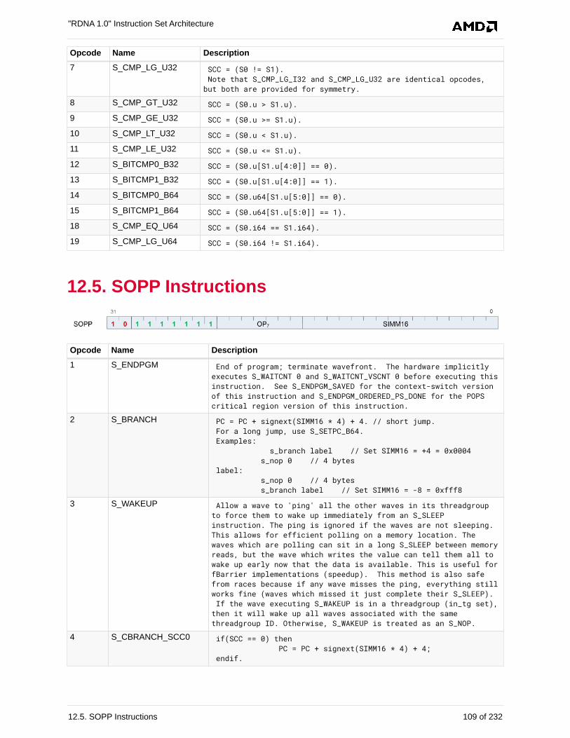
Opcode Name Description
7 S_CMP_LG_U32 SCC = (S0 != S1). Note that S_CMP_LG_I32 and S_CMP_LG_U32 are identical opcodes,but both are provided for symmetry.
8 S_CMP_GT_U32 SCC = (S0.u > S1.u).
9 S_CMP_GE_U32 SCC = (S0.u >= S1.u).
10 S_CMP_LT_U32 SCC = (S0.u < S1.u).
11 S_CMP_LE_U32 SCC = (S0.u <= S1.u).
12 S_BITCMP0_B32 SCC = (S0.u[S1.u[4:0]] == 0).
13 S_BITCMP1_B32 SCC = (S0.u[S1.u[4:0]] == 1).
14 S_BITCMP0_B64 SCC = (S0.u64[S1.u[5:0]] == 0).
15 S_BITCMP1_B64 SCC = (S0.u64[S1.u[5:0]] == 1).
18 S_CMP_EQ_U64 SCC = (S0.i64 == S1.i64).
19 S_CMP_LG_U64 SCC = (S0.i64 != S1.i64).
12.5. SOPP Instructions
Opcode Name Description
1 S_ENDPGM End of program; terminate wavefront. The hardware implicitlyexecutes S_WAITCNT 0 and S_WAITCNT_VSCNT 0 before executing thisinstruction. See S_ENDPGM_SAVED for the context-switch versionof this instruction and S_ENDPGM_ORDERED_PS_DONE for the POPScritical region version of this instruction.
2 S_BRANCH PC = PC + signext(SIMM16 * 4) + 4. // short jump. For a long jump, use S_SETPC_B64. Examples: s_branch label // Set SIMM16 = +4 = 0x0004 s_nop 0 // 4 bytes label: s_nop 0 // 4 bytes s_branch label // Set SIMM16 = -8 = 0xfff8
3 S_WAKEUP Allow a wave to 'ping' all the other waves in its threadgroupto force them to wake up immediately from an S_SLEEPinstruction. The ping is ignored if the waves are not sleeping.This allows for efficient polling on a memory location. Thewaves which are polling can sit in a long S_SLEEP between memoryreads, but the wave which writes the value can tell them all towake up early now that the data is available. This is useful forfBarrier implementations (speedup). This method is also safefrom races because if any wave misses the ping, everything stillworks fine (waves which missed it just complete their S_SLEEP). If the wave executing S_WAKEUP is in a threadgroup (in_tg set),then it will wake up all waves associated with the samethreadgroup ID. Otherwise, S_WAKEUP is treated as an S_NOP.
4 S_CBRANCH_SCC0 if(SCC == 0) then PC = PC + signext(SIMM16 * 4) + 4; endif.
"RDNA 1.0" Instruction Set Architecture
12.5. SOPP Instructions 109 of 232
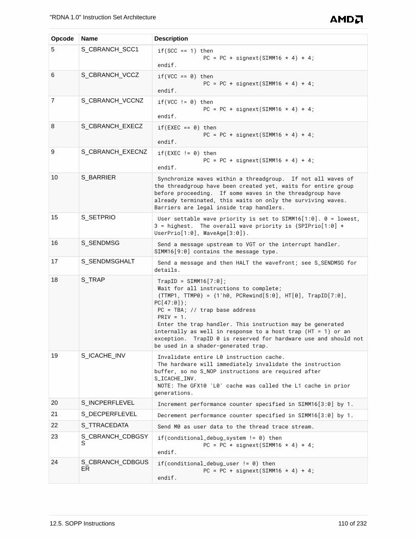
Opcode Name Description
5 S_CBRANCH_SCC1 if(SCC == 1) then PC = PC + signext(SIMM16 * 4) + 4; endif.
6 S_CBRANCH_VCCZ if(VCC == 0) then PC = PC + signext(SIMM16 * 4) + 4; endif.
7 S_CBRANCH_VCCNZ if(VCC != 0) then PC = PC + signext(SIMM16 * 4) + 4; endif.
8 S_CBRANCH_EXECZ if(EXEC == 0) then PC = PC + signext(SIMM16 * 4) + 4; endif.
9 S_CBRANCH_EXECNZ if(EXEC != 0) then PC = PC + signext(SIMM16 * 4) + 4; endif.
10 S_BARRIER Synchronize waves within a threadgroup. If not all waves ofthe threadgroup have been created yet, waits for entire groupbefore proceeding. If some waves in the threadgroup havealready terminated, this waits on only the surviving waves.Barriers are legal inside trap handlers.
15 S_SETPRIO User settable wave priority is set to SIMM16[1:0]. 0 = lowest,3 = highest. The overall wave priority is {SPIPrio[1:0] +UserPrio[1:0], WaveAge[3:0]}.
16 S_SENDMSG Send a message upstream to VGT or the interrupt handler.SIMM16[9:0] contains the message type.
17 S_SENDMSGHALT Send a message and then HALT the wavefront; see S_SENDMSG fordetails.
18 S_TRAP TrapID = SIMM16[7:0]; Wait for all instructions to complete; {TTMP1, TTMP0} = {1'h0, PCRewind[5:0], HT[0], TrapID[7:0],PC[47:0]}; PC = TBA; // trap base address PRIV = 1. Enter the trap handler. This instruction may be generatedinternally as well in response to a host trap (HT = 1) or anexception. TrapID 0 is reserved for hardware use and should notbe used in a shader-generated trap.
19 S_ICACHE_INV Invalidate entire L0 instruction cache. The hardware will immediately invalidate the instructionbuffer, so no S_NOP instructions are required afterS_ICACHE_INV. NOTE: The GFX10 'L0' cache was called the L1 cache in priorgenerations.
20 S_INCPERFLEVEL Increment performance counter specified in SIMM16[3:0] by 1.
21 S_DECPERFLEVEL Decrement performance counter specified in SIMM16[3:0] by 1.
22 S_TTRACEDATA Send M0 as user data to the thread trace stream.
23 S_CBRANCH_CDBGSYS
if(conditional_debug_system != 0) then PC = PC + signext(SIMM16 * 4) + 4; endif.
24 S_CBRANCH_CDBGUSER
if(conditional_debug_user != 0) then PC = PC + signext(SIMM16 * 4) + 4; endif.
"RDNA 1.0" Instruction Set Architecture
12.5. SOPP Instructions 110 of 232
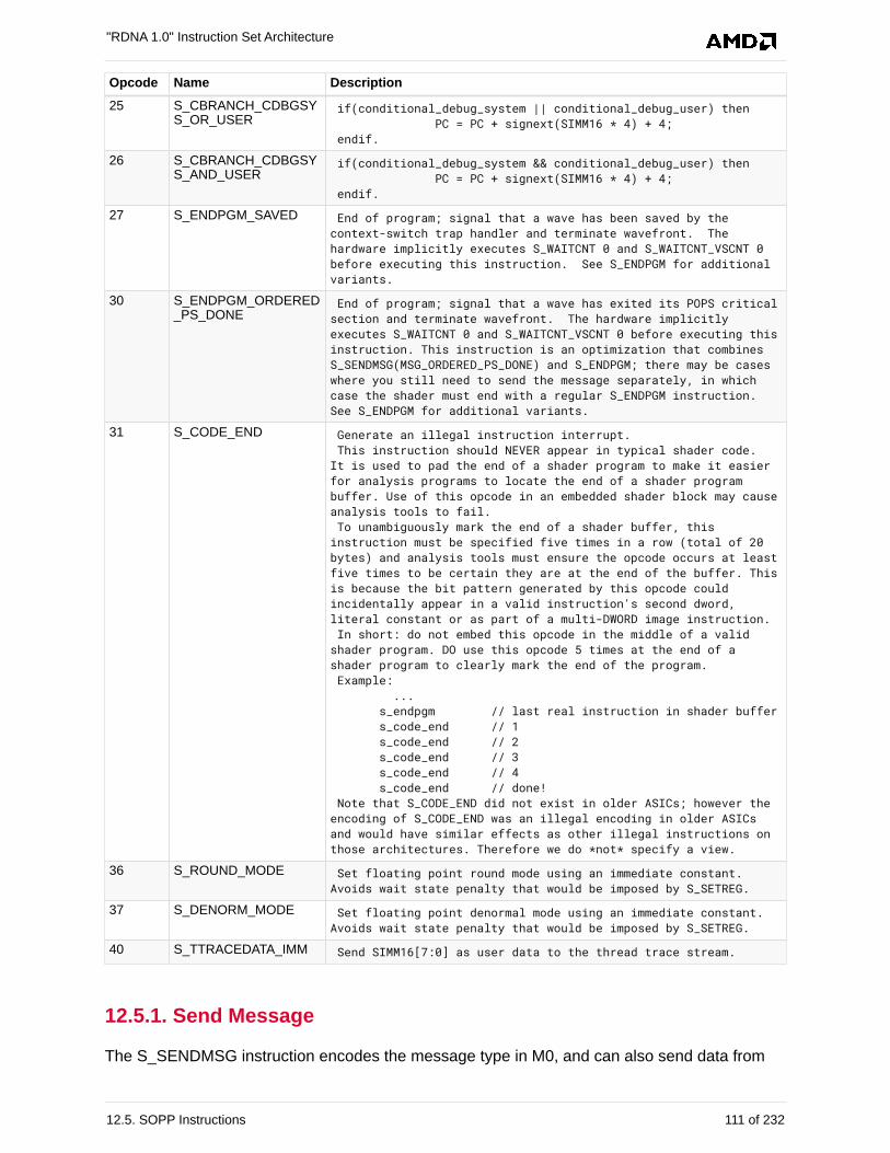
Opcode Name Description
25 S_CBRANCH_CDBGSYS_OR_USER
if(conditional_debug_system || conditional_debug_user) then PC = PC + signext(SIMM16 * 4) + 4; endif.
26 S_CBRANCH_CDBGSYS_AND_USER
if(conditional_debug_system && conditional_debug_user) then PC = PC + signext(SIMM16 * 4) + 4; endif.
27 S_ENDPGM_SAVED End of program; signal that a wave has been saved by thecontext-switch trap handler and terminate wavefront. Thehardware implicitly executes S_WAITCNT 0 and S_WAITCNT_VSCNT 0before executing this instruction. See S_ENDPGM for additionalvariants.
30 S_ENDPGM_ORDERED_PS_DONE
End of program; signal that a wave has exited its POPS criticalsection and terminate wavefront. The hardware implicitlyexecutes S_WAITCNT 0 and S_WAITCNT_VSCNT 0 before executing thisinstruction. This instruction is an optimization that combinesS_SENDMSG(MSG_ORDERED_PS_DONE) and S_ENDPGM; there may be caseswhere you still need to send the message separately, in whichcase the shader must end with a regular S_ENDPGM instruction.See S_ENDPGM for additional variants.
31 S_CODE_END Generate an illegal instruction interrupt. This instruction should NEVER appear in typical shader code.It is used to pad the end of a shader program to make it easierfor analysis programs to locate the end of a shader programbuffer. Use of this opcode in an embedded shader block may causeanalysis tools to fail. To unambiguously mark the end of a shader buffer, thisinstruction must be specified five times in a row (total of 20bytes) and analysis tools must ensure the opcode occurs at leastfive times to be certain they are at the end of the buffer. Thisis because the bit pattern generated by this opcode couldincidentally appear in a valid instruction's second dword,literal constant or as part of a multi-DWORD image instruction. In short: do not embed this opcode in the middle of a validshader program. DO use this opcode 5 times at the end of ashader program to clearly mark the end of the program. Example: ... s_endpgm // last real instruction in shader buffer s_code_end // 1 s_code_end // 2 s_code_end // 3 s_code_end // 4 s_code_end // done! Note that S_CODE_END did not exist in older ASICs; however theencoding of S_CODE_END was an illegal encoding in older ASICsand would have similar effects as other illegal instructions onthose architectures. Therefore we do *not* specify a view.
36 S_ROUND_MODE Set floating point round mode using an immediate constant.Avoids wait state penalty that would be imposed by S_SETREG.
37 S_DENORM_MODE Set floating point denormal mode using an immediate constant.Avoids wait state penalty that would be imposed by S_SETREG.
40 S_TTRACEDATA_IMM Send SIMM16[7:0] as user data to the thread trace stream.
12.5.1. Send Message
The S_SENDMSG instruction encodes the message type in M0, and can also send data from
"RDNA 1.0" Instruction Set Architecture
12.5. SOPP Instructions 111 of 232
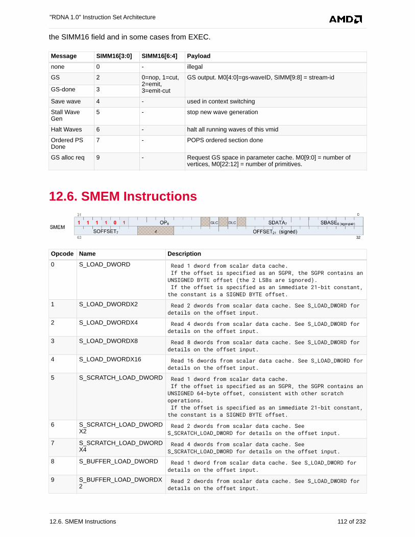
the SIMM16 field and in some cases from EXEC.
Message SIMM16[3:0] SIMM16[6:4] Payload
none 0 - illegal
GS 2 0=nop, 1=cut,2=emit,3=emit-cut
GS output. M0[4:0]=gs-waveID, SIMM[9:8] = stream-id
GS-done 3
Save wave 4 - used in context switching
Stall WaveGen
5 - stop new wave generation
Halt Waves 6 - halt all running waves of this vmid
Ordered PSDone
7 - POPS ordered section done
GS alloc req 9 - Request GS space in parameter cache. M0[9:0] = number ofvertices, M0[22:12] = number of primitives.
12.6. SMEM Instructions
Opcode Name Description
0 S_LOAD_DWORD Read 1 dword from scalar data cache. If the offset is specified as an SGPR, the SGPR contains anUNSIGNED BYTE offset (the 2 LSBs are ignored). If the offset is specified as an immediate 21-bit constant,the constant is a SIGNED BYTE offset.
1 S_LOAD_DWORDX2 Read 2 dwords from scalar data cache. See S_LOAD_DWORD fordetails on the offset input.
2 S_LOAD_DWORDX4 Read 4 dwords from scalar data cache. See S_LOAD_DWORD fordetails on the offset input.
3 S_LOAD_DWORDX8 Read 8 dwords from scalar data cache. See S_LOAD_DWORD fordetails on the offset input.
4 S_LOAD_DWORDX16 Read 16 dwords from scalar data cache. See S_LOAD_DWORD fordetails on the offset input.
5 S_SCRATCH_LOAD_DWORD Read 1 dword from scalar data cache. If the offset is specified as an SGPR, the SGPR contains anUNSIGNED 64-byte offset, consistent with other scratchoperations. If the offset is specified as an immediate 21-bit constant,the constant is a SIGNED BYTE offset.
6 S_SCRATCH_LOAD_DWORDX2
Read 2 dwords from scalar data cache. SeeS_SCRATCH_LOAD_DWORD for details on the offset input.
7 S_SCRATCH_LOAD_DWORDX4
Read 4 dwords from scalar data cache. SeeS_SCRATCH_LOAD_DWORD for details on the offset input.
8 S_BUFFER_LOAD_DWORD Read 1 dword from scalar data cache. See S_LOAD_DWORD fordetails on the offset input.
9 S_BUFFER_LOAD_DWORDX2
Read 2 dwords from scalar data cache. See S_LOAD_DWORD fordetails on the offset input.
"RDNA 1.0" Instruction Set Architecture
12.6. SMEM Instructions 112 of 232
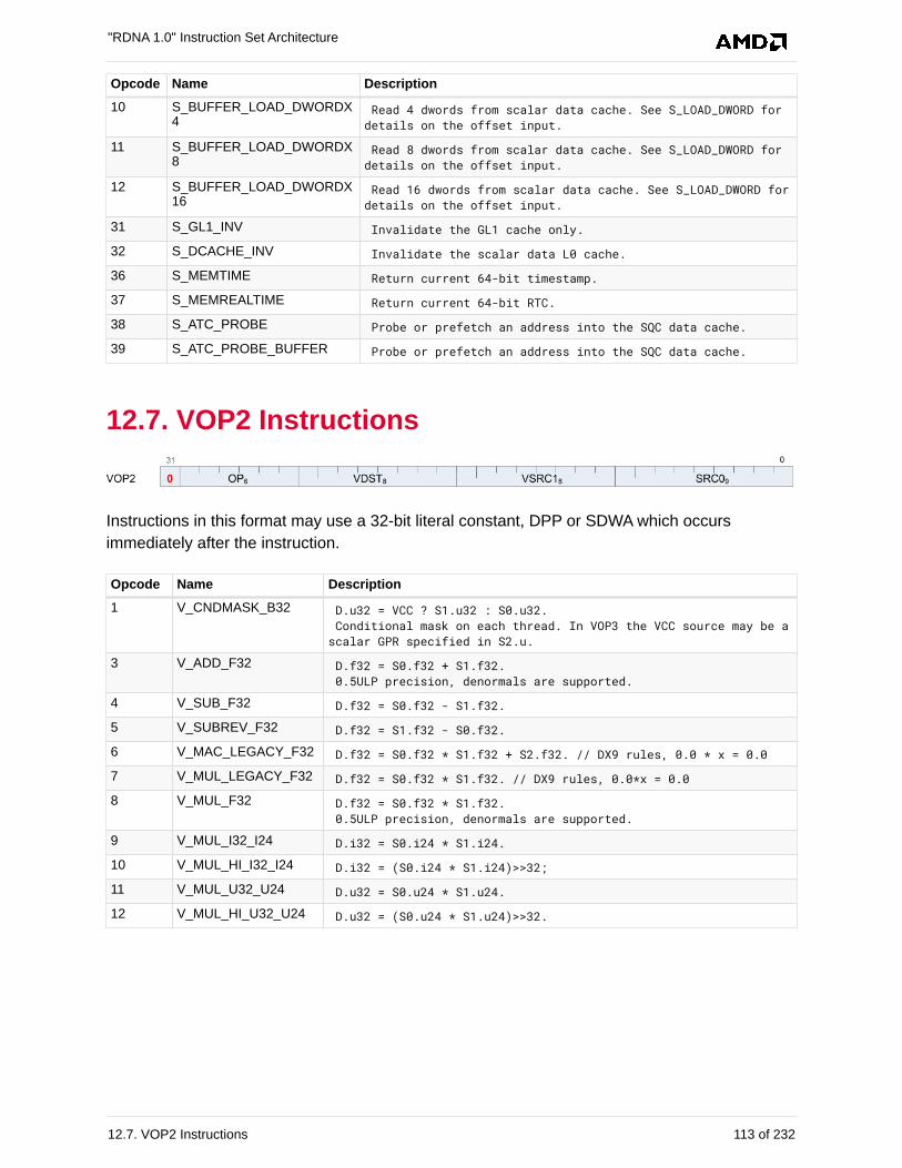
Opcode Name Description
10 S_BUFFER_LOAD_DWORDX4
Read 4 dwords from scalar data cache. See S_LOAD_DWORD fordetails on the offset input.
11 S_BUFFER_LOAD_DWORDX8
Read 8 dwords from scalar data cache. See S_LOAD_DWORD fordetails on the offset input.
12 S_BUFFER_LOAD_DWORDX16
Read 16 dwords from scalar data cache. See S_LOAD_DWORD fordetails on the offset input.
31 S_GL1_INV Invalidate the GL1 cache only.
32 S_DCACHE_INV Invalidate the scalar data L0 cache.
36 S_MEMTIME Return current 64-bit timestamp.
37 S_MEMREALTIME Return current 64-bit RTC.
38 S_ATC_PROBE Probe or prefetch an address into the SQC data cache.
39 S_ATC_PROBE_BUFFER Probe or prefetch an address into the SQC data cache.
12.7. VOP2 Instructions
Instructions in this format may use a 32-bit literal constant, DPP or SDWA which occurs
immediately after the instruction.
Opcode Name Description
1 V_CNDMASK_B32 D.u32 = VCC ? S1.u32 : S0.u32. Conditional mask on each thread. In VOP3 the VCC source may be ascalar GPR specified in S2.u.
3 V_ADD_F32 D.f32 = S0.f32 + S1.f32. 0.5ULP precision, denormals are supported.
4 V_SUB_F32 D.f32 = S0.f32 - S1.f32.
5 V_SUBREV_F32 D.f32 = S1.f32 - S0.f32.
6 V_MAC_LEGACY_F32 D.f32 = S0.f32 * S1.f32 + S2.f32. // DX9 rules, 0.0 * x = 0.0
7 V_MUL_LEGACY_F32 D.f32 = S0.f32 * S1.f32. // DX9 rules, 0.0*x = 0.0
8 V_MUL_F32 D.f32 = S0.f32 * S1.f32. 0.5ULP precision, denormals are supported.
9 V_MUL_I32_I24 D.i32 = S0.i24 * S1.i24.
10 V_MUL_HI_I32_I24 D.i32 = (S0.i24 * S1.i24)>>32;
11 V_MUL_U32_U24 D.u32 = S0.u24 * S1.u24.
12 V_MUL_HI_U32_U24 D.u32 = (S0.u24 * S1.u24)>>32.
"RDNA 1.0" Instruction Set Architecture
12.7. VOP2 Instructions 113 of 232
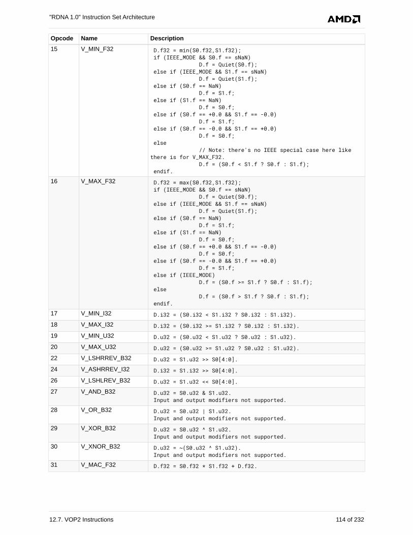
Opcode Name Description
15 V_MIN_F32 D.f32 = min(S0.f32,S1.f32); if (IEEE_MODE && S0.f == sNaN) D.f = Quiet(S0.f); else if (IEEE_MODE && S1.f == sNaN) D.f = Quiet(S1.f); else if (S0.f == NaN) D.f = S1.f; else if (S1.f == NaN) D.f = S0.f; else if (S0.f == +0.0 && S1.f == -0.0) D.f = S1.f; else if (S0.f == -0.0 && S1.f == +0.0) D.f = S0.f; else // Note: there's no IEEE special case here likethere is for V_MAX_F32. D.f = (S0.f < S1.f ? S0.f : S1.f); endif.
16 V_MAX_F32 D.f32 = max(S0.f32,S1.f32); if (IEEE_MODE && S0.f == sNaN) D.f = Quiet(S0.f); else if (IEEE_MODE && S1.f == sNaN) D.f = Quiet(S1.f); else if (S0.f == NaN) D.f = S1.f; else if (S1.f == NaN) D.f = S0.f; else if (S0.f == +0.0 && S1.f == -0.0) D.f = S0.f; else if (S0.f == -0.0 && S1.f == +0.0) D.f = S1.f; else if (IEEE_MODE) D.f = (S0.f >= S1.f ? S0.f : S1.f); else D.f = (S0.f > S1.f ? S0.f : S1.f); endif.
17 V_MIN_I32 D.i32 = (S0.i32 < S1.i32 ? S0.i32 : S1.i32).
18 V_MAX_I32 D.i32 = (S0.i32 >= S1.i32 ? S0.i32 : S1.i32).
19 V_MIN_U32 D.u32 = (S0.u32 < S1.u32 ? S0.u32 : S1.u32).
20 V_MAX_U32 D.u32 = (S0.u32 >= S1.u32 ? S0.u32 : S1.u32).
22 V_LSHRREV_B32 D.u32 = S1.u32 >> S0[4:0].
24 V_ASHRREV_I32 D.i32 = S1.i32 >> S0[4:0].
26 V_LSHLREV_B32 D.u32 = S1.u32 << S0[4:0].
27 V_AND_B32 D.u32 = S0.u32 & S1.u32. Input and output modifiers not supported.
28 V_OR_B32 D.u32 = S0.u32 | S1.u32. Input and output modifiers not supported.
29 V_XOR_B32 D.u32 = S0.u32 ^ S1.u32. Input and output modifiers not supported.
30 V_XNOR_B32 D.u32 = ~(S0.u32 ^ S1.u32). Input and output modifiers not supported.
31 V_MAC_F32 D.f32 = S0.f32 * S1.f32 + D.f32.
"RDNA 1.0" Instruction Set Architecture
12.7. VOP2 Instructions 114 of 232
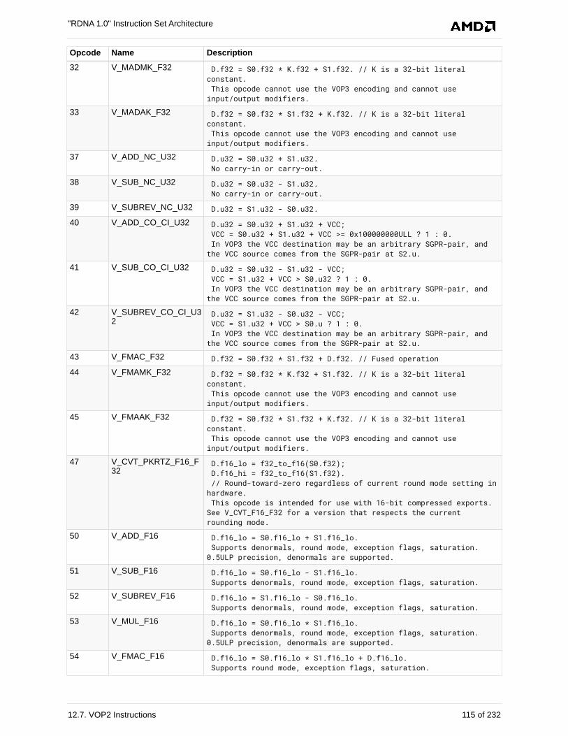
Opcode Name Description
32 V_MADMK_F32 D.f32 = S0.f32 * K.f32 + S1.f32. // K is a 32-bit literalconstant. This opcode cannot use the VOP3 encoding and cannot useinput/output modifiers.
33 V_MADAK_F32 D.f32 = S0.f32 * S1.f32 + K.f32. // K is a 32-bit literalconstant. This opcode cannot use the VOP3 encoding and cannot useinput/output modifiers.
37 V_ADD_NC_U32 D.u32 = S0.u32 + S1.u32. No carry-in or carry-out.
38 V_SUB_NC_U32 D.u32 = S0.u32 - S1.u32. No carry-in or carry-out.
39 V_SUBREV_NC_U32 D.u32 = S1.u32 - S0.u32.
40 V_ADD_CO_CI_U32 D.u32 = S0.u32 + S1.u32 + VCC; VCC = S0.u32 + S1.u32 + VCC >= 0x100000000ULL ? 1 : 0. In VOP3 the VCC destination may be an arbitrary SGPR-pair, andthe VCC source comes from the SGPR-pair at S2.u.
41 V_SUB_CO_CI_U32 D.u32 = S0.u32 - S1.u32 - VCC; VCC = S1.u32 + VCC > S0.u32 ? 1 : 0. In VOP3 the VCC destination may be an arbitrary SGPR-pair, andthe VCC source comes from the SGPR-pair at S2.u.
42 V_SUBREV_CO_CI_U32
D.u32 = S1.u32 - S0.u32 - VCC; VCC = S1.u32 + VCC > S0.u ? 1 : 0. In VOP3 the VCC destination may be an arbitrary SGPR-pair, andthe VCC source comes from the SGPR-pair at S2.u.
43 V_FMAC_F32 D.f32 = S0.f32 * S1.f32 + D.f32. // Fused operation
44 V_FMAMK_F32 D.f32 = S0.f32 * K.f32 + S1.f32. // K is a 32-bit literalconstant. This opcode cannot use the VOP3 encoding and cannot useinput/output modifiers.
45 V_FMAAK_F32 D.f32 = S0.f32 * S1.f32 + K.f32. // K is a 32-bit literalconstant. This opcode cannot use the VOP3 encoding and cannot useinput/output modifiers.
47 V_CVT_PKRTZ_F16_F32
D.f16_lo = f32_to_f16(S0.f32); D.f16_hi = f32_to_f16(S1.f32). // Round-toward-zero regardless of current round mode setting inhardware. This opcode is intended for use with 16-bit compressed exports.See V_CVT_F16_F32 for a version that respects the currentrounding mode.
50 V_ADD_F16 D.f16_lo = S0.f16_lo + S1.f16_lo. Supports denormals, round mode, exception flags, saturation.0.5ULP precision, denormals are supported.
51 V_SUB_F16 D.f16_lo = S0.f16_lo - S1.f16_lo. Supports denormals, round mode, exception flags, saturation.
52 V_SUBREV_F16 D.f16_lo = S1.f16_lo - S0.f16_lo. Supports denormals, round mode, exception flags, saturation.
53 V_MUL_F16 D.f16_lo = S0.f16_lo * S1.f16_lo. Supports denormals, round mode, exception flags, saturation.0.5ULP precision, denormals are supported.
54 V_FMAC_F16 D.f16_lo = S0.f16_lo * S1.f16_lo + D.f16_lo. Supports round mode, exception flags, saturation.
"RDNA 1.0" Instruction Set Architecture
12.7. VOP2 Instructions 115 of 232
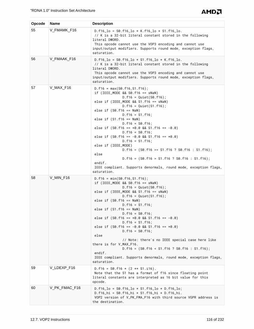
Opcode Name Description
55 V_FMAMK_F16 D.f16_lo = S0.f16_lo * K.f16_lo + S1.f16_lo. // K is a 32-bit literal constant stored in the followingliteral DWORD. This opcode cannot use the VOP3 encoding and cannot useinput/output modifiers. Supports round mode, exception flags,saturation.
56 V_FMAAK_F16 D.f16_lo = S0.f16_lo * S1.f16_lo + K.f16_lo. // K is a 32-bit literal constant stored in the followingliteral DWORD. This opcode cannot use the VOP3 encoding and cannot useinput/output modifiers. Supports round mode, exception flags,saturation.
57 V_MAX_F16 D.f16 = max(S0.f16,S1.f16); if (IEEE_MODE && S0.f16 == sNaN) D.f16 = Quiet(S0.f16); else if (IEEE_MODE && S1.f16 == sNaN) D.f16 = Quiet(S1.f16); else if (S0.f16 == NaN) D.f16 = S1.f16; else if (S1.f16 == NaN) D.f16 = S0.f16; else if (S0.f16 == +0.0 && S1.f16 == -0.0) D.f16 = S0.f16; else if (S0.f16 == -0.0 && S1.f16 == +0.0) D.f16 = S1.f16; else if (IEEE_MODE) D.f16 = (S0.f16 >= S1.f16 ? S0.f16 : S1.f16); else D.f16 = (S0.f16 > S1.f16 ? S0.f16 : S1.f16); endif. IEEE compliant. Supports denormals, round mode, exception flags,saturation.
58 V_MIN_F16 D.f16 = min(S0.f16,S1.f16); if (IEEE_MODE && S0.f16 == sNaN) D.f16 = Quiet(S0.f16); else if (IEEE_MODE && S1.f16 == sNaN) D.f16 = Quiet(S1.f16); else if (S0.f16 == NaN) D.f16 = S1.f16; else if (S1.f16 == NaN) D.f16 = S0.f16; else if (S0.f16 == +0.0 && S1.f16 == -0.0) D.f16 = S1.f16; else if (S0.f16 == -0.0 && S1.f16 == +0.0) D.f16 = S0.f16; else // Note: there's no IEEE special case here likethere is for V_MAX_F16. D.f16 = (S0.f16 < S1.f16 ? S0.f16 : S1.f16); endif. IEEE compliant. Supports denormals, round mode, exception flags,saturation.
59 V_LDEXP_F16 D.f16 = S0.f16 * (2 ** S1.i16). Note that the S1 has a format of f16 since floating pointliteral constants are interpreted as 16 bit value for thisopcode.
60 V_PK_FMAC_F16 D.f16_lo = S0.f16_lo * S1.f16_lo + D.f16_lo; D.f16_hi = S0.f16_hi * S1.f16_hi + D.f16_hi. VOP2 version of V_PK_FMA_F16 with third source VGPR address isthe destination.
"RDNA 1.0" Instruction Set Architecture
12.7. VOP2 Instructions 116 of 232
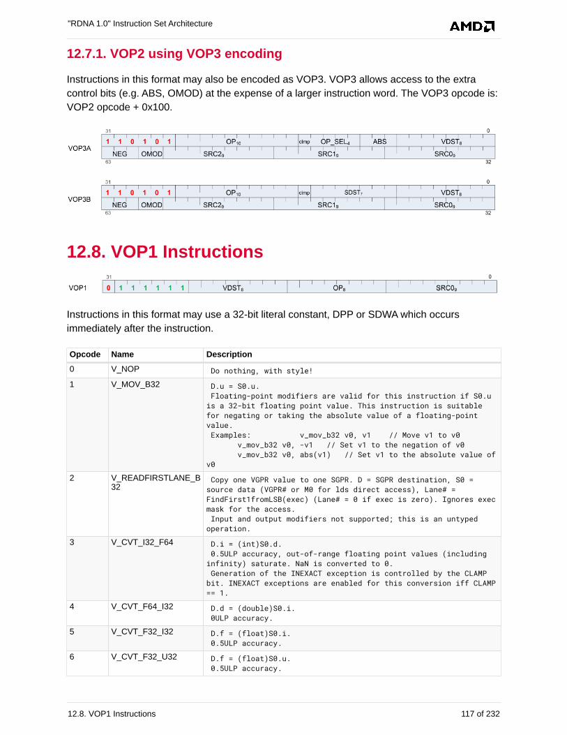
12.7.1. VOP2 using VOP3 encoding
Instructions in this format may also be encoded as VOP3. VOP3 allows access to the extra
control bits (e.g. ABS, OMOD) at the expense of a larger instruction word. The VOP3 opcode is:
VOP2 opcode + 0x100.
12.8. VOP1 Instructions
Instructions in this format may use a 32-bit literal constant, DPP or SDWA which occurs
immediately after the instruction.
Opcode Name Description
0 V_NOP Do nothing, with style!
1 V_MOV_B32 D.u = S0.u. Floating-point modifiers are valid for this instruction if S0.uis a 32-bit floating point value. This instruction is suitablefor negating or taking the absolute value of a floating-pointvalue. Examples: v_mov_b32 v0, v1 // Move v1 to v0 v_mov_b32 v0, -v1 // Set v1 to the negation of v0 v_mov_b32 v0, abs(v1) // Set v1 to the absolute value ofv0
2 V_READFIRSTLANE_B32
Copy one VGPR value to one SGPR. D = SGPR destination, S0 =source data (VGPR# or M0 for lds direct access), Lane# =FindFirst1fromLSB(exec) (Lane# = 0 if exec is zero). Ignores execmask for the access. Input and output modifiers not supported; this is an untypedoperation.
3 V_CVT_I32_F64 D.i = (int)S0.d. 0.5ULP accuracy, out-of-range floating point values (includinginfinity) saturate. NaN is converted to 0. Generation of the INEXACT exception is controlled by the CLAMPbit. INEXACT exceptions are enabled for this conversion iff CLAMP== 1.
4 V_CVT_F64_I32 D.d = (double)S0.i. 0ULP accuracy.
5 V_CVT_F32_I32 D.f = (float)S0.i. 0.5ULP accuracy.
6 V_CVT_F32_U32 D.f = (float)S0.u. 0.5ULP accuracy.
"RDNA 1.0" Instruction Set Architecture
12.8. VOP1 Instructions 117 of 232
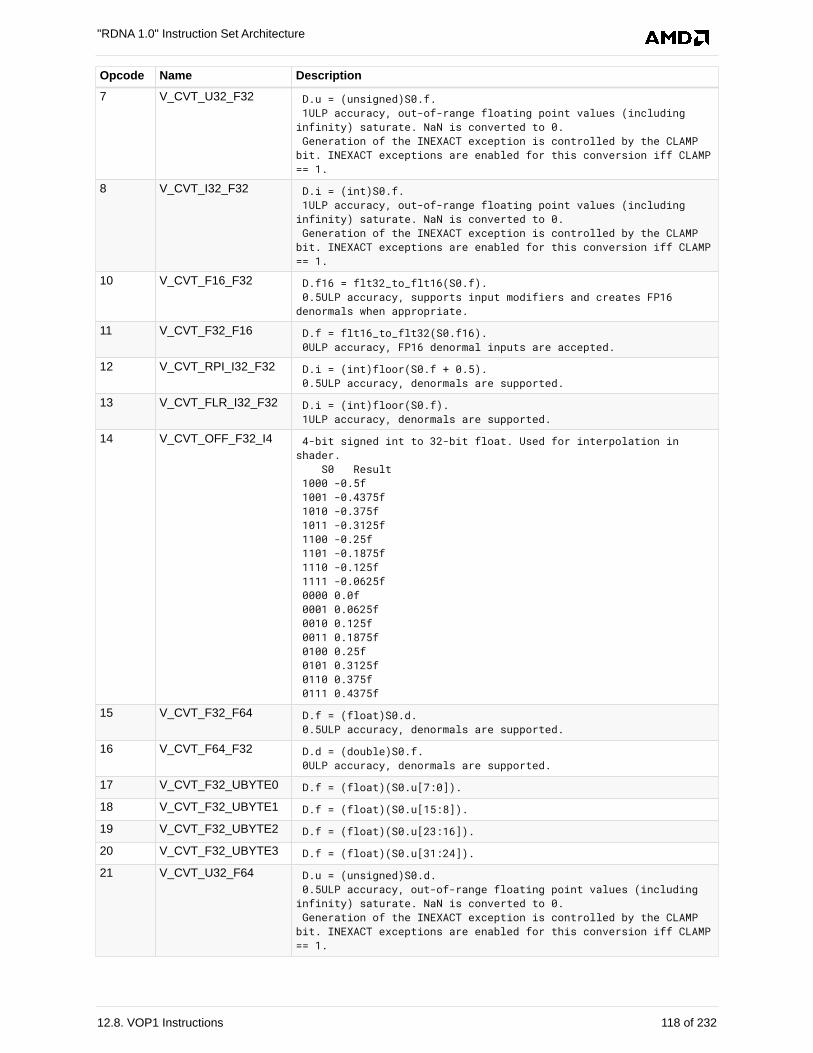
Opcode Name Description
7 V_CVT_U32_F32 D.u = (unsigned)S0.f. 1ULP accuracy, out-of-range floating point values (includinginfinity) saturate. NaN is converted to 0. Generation of the INEXACT exception is controlled by the CLAMPbit. INEXACT exceptions are enabled for this conversion iff CLAMP== 1.
8 V_CVT_I32_F32 D.i = (int)S0.f. 1ULP accuracy, out-of-range floating point values (includinginfinity) saturate. NaN is converted to 0. Generation of the INEXACT exception is controlled by the CLAMPbit. INEXACT exceptions are enabled for this conversion iff CLAMP== 1.
10 V_CVT_F16_F32 D.f16 = flt32_to_flt16(S0.f). 0.5ULP accuracy, supports input modifiers and creates FP16denormals when appropriate.
11 V_CVT_F32_F16 D.f = flt16_to_flt32(S0.f16). 0ULP accuracy, FP16 denormal inputs are accepted.
12 V_CVT_RPI_I32_F32 D.i = (int)floor(S0.f + 0.5). 0.5ULP accuracy, denormals are supported.
13 V_CVT_FLR_I32_F32 D.i = (int)floor(S0.f). 1ULP accuracy, denormals are supported.
14 V_CVT_OFF_F32_I4 4-bit signed int to 32-bit float. Used for interpolation inshader. S0 Result 1000 -0.5f 1001 -0.4375f 1010 -0.375f 1011 -0.3125f 1100 -0.25f 1101 -0.1875f 1110 -0.125f 1111 -0.0625f 0000 0.0f 0001 0.0625f 0010 0.125f 0011 0.1875f 0100 0.25f 0101 0.3125f 0110 0.375f 0111 0.4375f
15 V_CVT_F32_F64 D.f = (float)S0.d. 0.5ULP accuracy, denormals are supported.
16 V_CVT_F64_F32 D.d = (double)S0.f. 0ULP accuracy, denormals are supported.
17 V_CVT_F32_UBYTE0 D.f = (float)(S0.u[7:0]).
18 V_CVT_F32_UBYTE1 D.f = (float)(S0.u[15:8]).
19 V_CVT_F32_UBYTE2 D.f = (float)(S0.u[23:16]).
20 V_CVT_F32_UBYTE3 D.f = (float)(S0.u[31:24]).
21 V_CVT_U32_F64 D.u = (unsigned)S0.d. 0.5ULP accuracy, out-of-range floating point values (includinginfinity) saturate. NaN is converted to 0. Generation of the INEXACT exception is controlled by the CLAMPbit. INEXACT exceptions are enabled for this conversion iff CLAMP== 1.
"RDNA 1.0" Instruction Set Architecture
12.8. VOP1 Instructions 118 of 232
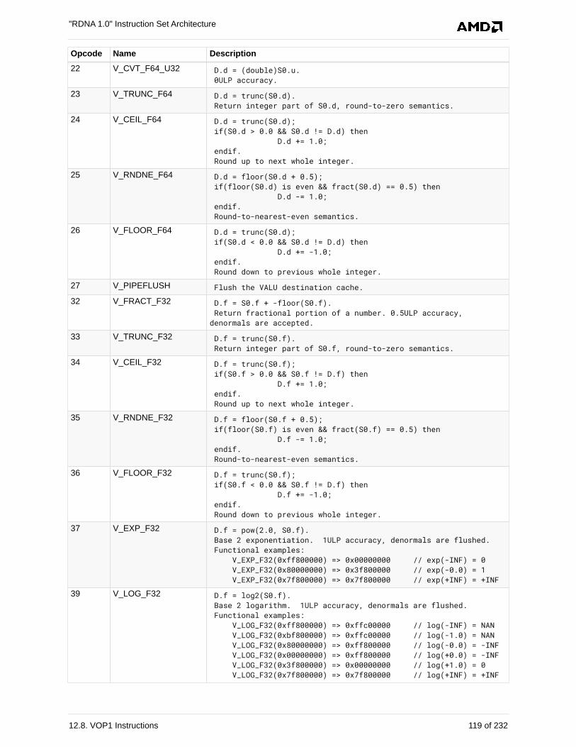
Opcode Name Description
22 V_CVT_F64_U32 D.d = (double)S0.u. 0ULP accuracy.
23 V_TRUNC_F64 D.d = trunc(S0.d). Return integer part of S0.d, round-to-zero semantics.
24 V_CEIL_F64 D.d = trunc(S0.d); if(S0.d > 0.0 && S0.d != D.d) then D.d += 1.0; endif. Round up to next whole integer.
25 V_RNDNE_F64 D.d = floor(S0.d + 0.5); if(floor(S0.d) is even && fract(S0.d) == 0.5) then D.d -= 1.0; endif. Round-to-nearest-even semantics.
26 V_FLOOR_F64 D.d = trunc(S0.d); if(S0.d < 0.0 && S0.d != D.d) then D.d += -1.0; endif. Round down to previous whole integer.
27 V_PIPEFLUSH Flush the VALU destination cache.
32 V_FRACT_F32 D.f = S0.f + -floor(S0.f). Return fractional portion of a number. 0.5ULP accuracy,denormals are accepted.
33 V_TRUNC_F32 D.f = trunc(S0.f). Return integer part of S0.f, round-to-zero semantics.
34 V_CEIL_F32 D.f = trunc(S0.f); if(S0.f > 0.0 && S0.f != D.f) then D.f += 1.0; endif. Round up to next whole integer.
35 V_RNDNE_F32 D.f = floor(S0.f + 0.5); if(floor(S0.f) is even && fract(S0.f) == 0.5) then D.f -= 1.0; endif. Round-to-nearest-even semantics.
36 V_FLOOR_F32 D.f = trunc(S0.f); if(S0.f < 0.0 && S0.f != D.f) then D.f += -1.0; endif. Round down to previous whole integer.
37 V_EXP_F32 D.f = pow(2.0, S0.f). Base 2 exponentiation. 1ULP accuracy, denormals are flushed. Functional examples: V_EXP_F32(0xff800000) => 0x00000000 // exp(-INF) = 0 V_EXP_F32(0x80000000) => 0x3f800000 // exp(-0.0) = 1 V_EXP_F32(0x7f800000) => 0x7f800000 // exp(+INF) = +INF
39 V_LOG_F32 D.f = log2(S0.f). Base 2 logarithm. 1ULP accuracy, denormals are flushed. Functional examples: V_LOG_F32(0xff800000) => 0xffc00000 // log(-INF) = NAN V_LOG_F32(0xbf800000) => 0xffc00000 // log(-1.0) = NAN V_LOG_F32(0x80000000) => 0xff800000 // log(-0.0) = -INF V_LOG_F32(0x00000000) => 0xff800000 // log(+0.0) = -INF V_LOG_F32(0x3f800000) => 0x00000000 // log(+1.0) = 0 V_LOG_F32(0x7f800000) => 0x7f800000 // log(+INF) = +INF
"RDNA 1.0" Instruction Set Architecture
12.8. VOP1 Instructions 119 of 232
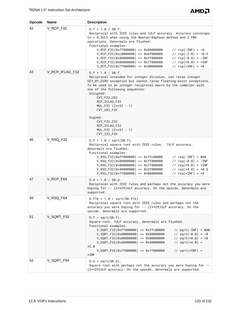
Opcode Name Description
42 V_RCP_F32 D.f = 1.0 / S0.f. Reciprocal with IEEE rules and 1ULP accuracy. Accuracy convergesto < 0.5ULP when using the Newton-Raphson method and 2 FMAoperations. Denormals are flushed. Functional examples: V_RCP_F32(0xff800000) => 0x80000000 // rcp(-INF) = -0 V_RCP_F32(0xc0000000) => 0xbf000000 // rcp(-2.0) = -0.5 V_RCP_F32(0x80000000) => 0xff800000 // rcp(-0.0) = -INF V_RCP_F32(0x00000000) => 0x7f800000 // rcp(+0.0) = +INF V_RCP_F32(0x7f800000) => 0x00000000 // rcp(+INF) = +0
43 V_RCP_IFLAG_F32 D.f = 1.0 / S0.f. Reciprocal intended for integer division, can raise integerDIV_BY_ZERO exception but cannot raise floating-point exceptions.To be used in an integer reciprocal macro by the compiler withone of the following sequences: Unsigned: CVT_F32_U32 RCP_IFLAG_F32 MUL_F32 (2**32 - 1) CVT_U32_F32
Signed: CVT_F32_I32 RCP_IFLAG_F32 MUL_F32 (2**31 - 1) CVT_I32_F32
46 V_RSQ_F32 D.f = 1.0 / sqrt(S0.f). Reciprocal square root with IEEE rules. 1ULP accuracy,denormals are flushed. Functional examples: V_RSQ_F32(0xff800000) => 0xffc00000 // rsq(-INF) = NAN V_RSQ_F32(0x80000000) => 0xff800000 // rsq(-0.0) = -INF V_RSQ_F32(0x00000000) => 0x7f800000 // rsq(+0.0) = +INF V_RSQ_F32(0x40800000) => 0x3f000000 // rsq(+4.0) = +0.5 V_RSQ_F32(0x7f800000) => 0x00000000 // rsq(+INF) = +0
47 V_RCP_F64 D.d = 1.0 / S0.d. Reciprocal with IEEE rules and perhaps not the accuracy you werehoping for -- (2**29)ULP accuracy. On the upside, denormals aresupported.
49 V_RSQ_F64 D.f16 = 1.0 / sqrt(S0.f16). Reciprocal square root with IEEE rules and perhaps not theaccuracy you were hoping for -- (2**29)ULP accuracy. On theupside, denormals are supported.
51 V_SQRT_F32 D.f = sqrt(S0.f). Square root. 1ULP accuracy, denormals are flushed. Functional examples: V_SQRT_F32(0xff800000) => 0xffc00000 // sqrt(-INF) = NAN V_SQRT_F32(0x80000000) => 0x80000000 // sqrt(-0.0) = -0 V_SQRT_F32(0x00000000) => 0x00000000 // sqrt(+0.0) = +0 V_SQRT_F32(0x40800000) => 0x40000000 // sqrt(+4.0) =+2.0 V_SQRT_F32(0x7f800000) => 0x7f800000 // sqrt(+INF) =+INF
52 V_SQRT_F64 D.d = sqrt(S0.d). Square root with perhaps not the accuracy you were hoping for --(2**29)ULP accuracy. On the upside, denormals are supported.
"RDNA 1.0" Instruction Set Architecture
12.8. VOP1 Instructions 120 of 232
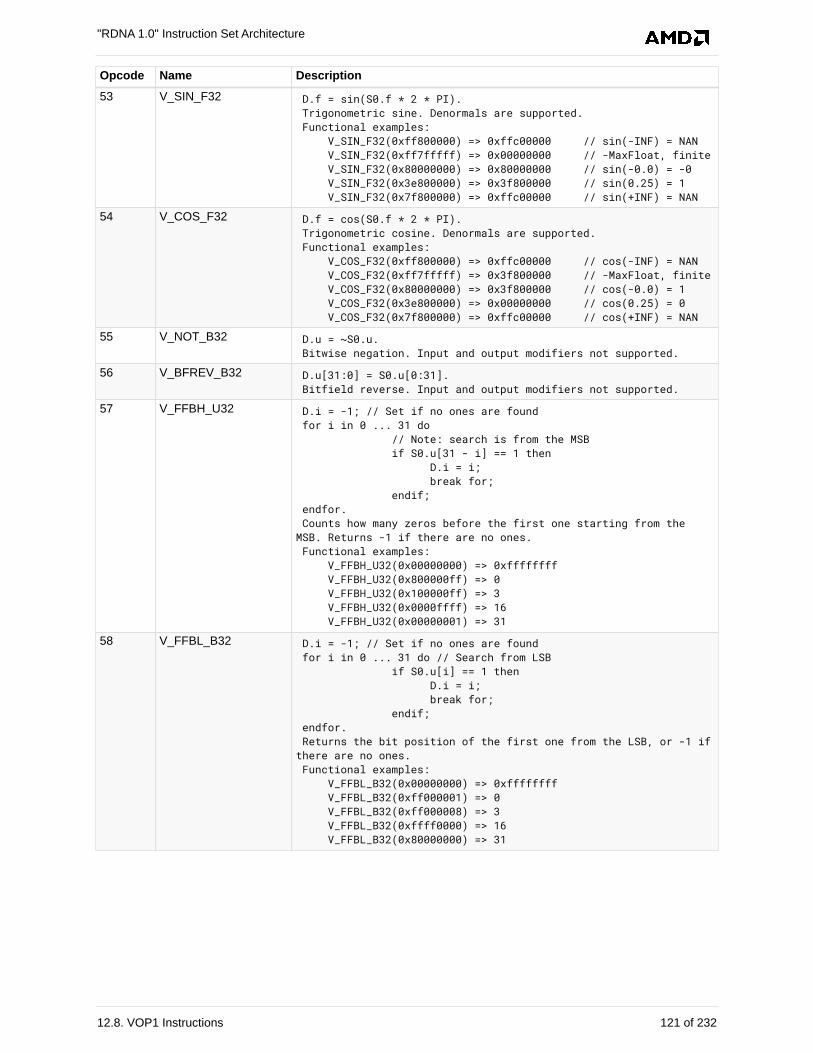
Opcode Name Description
53 V_SIN_F32 D.f = sin(S0.f * 2 * PI). Trigonometric sine. Denormals are supported. Functional examples: V_SIN_F32(0xff800000) => 0xffc00000 // sin(-INF) = NAN V_SIN_F32(0xff7fffff) => 0x00000000 // -MaxFloat, finite V_SIN_F32(0x80000000) => 0x80000000 // sin(-0.0) = -0 V_SIN_F32(0x3e800000) => 0x3f800000 // sin(0.25) = 1 V_SIN_F32(0x7f800000) => 0xffc00000 // sin(+INF) = NAN
54 V_COS_F32 D.f = cos(S0.f * 2 * PI). Trigonometric cosine. Denormals are supported. Functional examples: V_COS_F32(0xff800000) => 0xffc00000 // cos(-INF) = NAN V_COS_F32(0xff7fffff) => 0x3f800000 // -MaxFloat, finite V_COS_F32(0x80000000) => 0x3f800000 // cos(-0.0) = 1 V_COS_F32(0x3e800000) => 0x00000000 // cos(0.25) = 0 V_COS_F32(0x7f800000) => 0xffc00000 // cos(+INF) = NAN
55 V_NOT_B32 D.u = ~S0.u. Bitwise negation. Input and output modifiers not supported.
56 V_BFREV_B32 D.u[31:0] = S0.u[0:31]. Bitfield reverse. Input and output modifiers not supported.
57 V_FFBH_U32 D.i = -1; // Set if no ones are found for i in 0 ... 31 do // Note: search is from the MSB if S0.u[31 - i] == 1 then D.i = i; break for; endif; endfor. Counts how many zeros before the first one starting from theMSB. Returns -1 if there are no ones. Functional examples: V_FFBH_U32(0x00000000) => 0xffffffff V_FFBH_U32(0x800000ff) => 0 V_FFBH_U32(0x100000ff) => 3 V_FFBH_U32(0x0000ffff) => 16 V_FFBH_U32(0x00000001) => 31
58 V_FFBL_B32 D.i = -1; // Set if no ones are found for i in 0 ... 31 do // Search from LSB if S0.u[i] == 1 then D.i = i; break for; endif; endfor. Returns the bit position of the first one from the LSB, or -1 ifthere are no ones. Functional examples: V_FFBL_B32(0x00000000) => 0xffffffff V_FFBL_B32(0xff000001) => 0 V_FFBL_B32(0xff000008) => 3 V_FFBL_B32(0xffff0000) => 16 V_FFBL_B32(0x80000000) => 31
"RDNA 1.0" Instruction Set Architecture
12.8. VOP1 Instructions 121 of 232
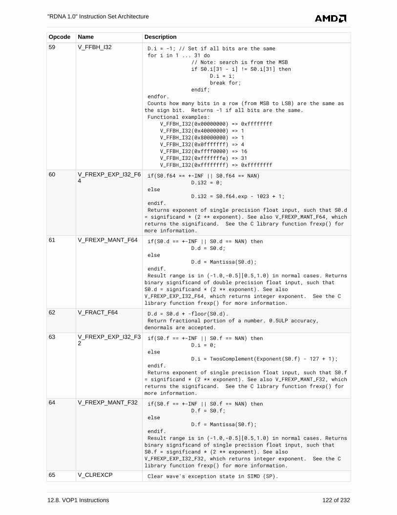
Opcode Name Description
59 V_FFBH_I32 D.i = -1; // Set if all bits are the same for i in 1 ... 31 do // Note: search is from the MSB if S0.i[31 - i] != S0.i[31] then D.i = i; break for; endif; endfor. Counts how many bits in a row (from MSB to LSB) are the same asthe sign bit. Returns -1 if all bits are the same. Functional examples: V_FFBH_I32(0x00000000) => 0xffffffff V_FFBH_I32(0x40000000) => 1 V_FFBH_I32(0x80000000) => 1 V_FFBH_I32(0x0fffffff) => 4 V_FFBH_I32(0xffff0000) => 16 V_FFBH_I32(0xfffffffe) => 31 V_FFBH_I32(0xffffffff) => 0xffffffff
60 V_FREXP_EXP_I32_F64
if(S0.f64 == +-INF || S0.f64 == NAN) D.i32 = 0; else D.i32 = S0.f64.exp - 1023 + 1; endif. Returns exponent of single precision float input, such that S0.d= significand * (2 ** exponent). See also V_FREXP_MANT_F64, whichreturns the significand. See the C library function frexp() formore information.
61 V_FREXP_MANT_F64 if(S0.d == +-INF || S0.d == NAN) then D.d = S0.d; else D.d = Mantissa(S0.d); endif. Result range is in (-1.0,-0.5][0.5,1.0) in normal cases. Returnsbinary significand of double precision float input, such thatS0.d = significand * (2 ** exponent). See alsoV_FREXP_EXP_I32_F64, which returns integer exponent. See the Clibrary function frexp() for more information.
62 V_FRACT_F64 D.d = S0.d + -floor(S0.d). Return fractional portion of a number. 0.5ULP accuracy,denormals are accepted.
63 V_FREXP_EXP_I32_F32
if(S0.f == +-INF || S0.f == NAN) then D.i = 0; else D.i = TwosComplement(Exponent(S0.f) - 127 + 1); endif. Returns exponent of single precision float input, such that S0.f= significand * (2 ** exponent). See also V_FREXP_MANT_F32, whichreturns the significand. See the C library function frexp() formore information.
64 V_FREXP_MANT_F32 if(S0.f == +-INF || S0.f == NAN) then D.f = S0.f; else D.f = Mantissa(S0.f); endif. Result range is in (-1.0,-0.5][0.5,1.0) in normal cases. Returnsbinary significand of single precision float input, such thatS0.f = significand * (2 ** exponent). See alsoV_FREXP_EXP_I32_F32, which returns integer exponent. See the Clibrary function frexp() for more information.
65 V_CLREXCP Clear wave's exception state in SIMD (SP).
"RDNA 1.0" Instruction Set Architecture
12.8. VOP1 Instructions 122 of 232
Opcode Name Description
66 V_MOVRELD_B32 addr = VGPR address appearing in instruction DST field; addr += M0.u[31:0]; VGPR[addr].u = S0.u. Move to a relative destination address. The followinginstruction sequence will perform a move v15 <== v7: s_mov_b32 m0, 10 v_movreld_b32 v5, v7
67 V_MOVRELS_B32 addr = VGPR address appearing in instruction SRC0 field; addr += M0.u[31:0]; D.u = VGPR[addr].u. Move from a relative source address. The following instructionsequence will perform a move v5 <== v17: s_mov_b32 m0, 10 v_movrels_b32 v5, v7
68 V_MOVRELSD_B32 addr_src = VGPR address appearing in instruction SRC0 field; addr_src += M0.u[31:0]; addr_dst = VGPR address appearing in instruction DST field; addr_dst += M0.u[31:0]; VGPR[addr_dst].u = VGPR[addr_src].u. Move from a relative source address to a relative destinationaddress. The following instruction sequence will perform a movev15 <== v17: s_mov_b32 m0, 10 v_movrelsd_b32 v5, v7
72 V_MOVRELSD_2_B32 addr_src = VGPR address appearing in instruction SRC0 field; addr_src += M0.u[9:0]; addr_dst = VGPR address appearing in instruction DST field; addr_dst += M0.u[25:16]; VGPR[addr_dst].u = VGPR[addr_src].u. Move from a relative source address to a relative destinationaddress, with different relative offsets. The followinginstruction sequence will perform a move v25 <== v17: s_mov_b32 m0, ((20 << 16) | 10) v_movrelsd_2_b32 v5, v7
80 V_CVT_F16_U16 D.f16 = uint16_to_flt16(S.u16). 0.5ULP accuracy, supports denormals, rounding, exception flagsand saturation.
81 V_CVT_F16_I16 D.f16 = int16_to_flt16(S.i16). 0.5ULP accuracy, supports denormals, rounding, exception flagsand saturation.
82 V_CVT_U16_F16 D.u16 = flt16_to_uint16(S.f16). 1ULP accuracy, supports rounding, exception flags andsaturation. FP16 denormals are accepted. Conversion is done withtruncation. Generation of the INEXACT exception is controlled by the CLAMPbit. INEXACT exceptions are enabled for this conversion iff CLAMP== 1.
83 V_CVT_I16_F16 D.i16 = flt16_to_int16(S.f16). 1ULP accuracy, supports rounding, exception flags andsaturation. FP16 denormals are accepted. Conversion is done withtruncation. Generation of the INEXACT exception is controlled by the CLAMPbit. INEXACT exceptions are enabled for this conversion iff CLAMP== 1.
"RDNA 1.0" Instruction Set Architecture
12.8. VOP1 Instructions 123 of 232

Opcode Name Description
84 V_RCP_F16 D.f16 = 1.0 / S0.f16. Reciprocal with IEEE rules and 0.51ULP accuracy. Functional examples: V_RCP_F16(0xfc00) => 0x8000 // rcp(-INF) = -0 V_RCP_F16(0xc000) => 0xb800 // rcp(-2.0) = -0.5 V_RCP_F16(0x8000) => 0xfc00 // rcp(-0.0) = -INF V_RCP_F16(0x0000) => 0x7c00 // rcp(+0.0) = +INF V_RCP_F16(0x7c00) => 0x0000 // rcp(+INF) = +0
85 V_SQRT_F16 D.f16 = sqrt(S0.f16). Square root. 0.51ULP accuracy, denormals are supported. Functional examples: V_SQRT_F16(0xfc00) => 0xfe00 // sqrt(-INF) = NAN V_SQRT_F16(0x8000) => 0x8000 // sqrt(-0.0) = -0 V_SQRT_F16(0x0000) => 0x0000 // sqrt(+0.0) = +0 V_SQRT_F16(0x4400) => 0x4000 // sqrt(+4.0) = +2.0 V_SQRT_F16(0x7c00) => 0x7c00 // sqrt(+INF) = +INF
86 V_RSQ_F16 D.f16 = 1.0 / sqrt(S0.f16). Reciprocal square root with IEEE rules. 0.51ULP accuracy,denormals are supported. Functional examples: V_RSQ_F16(0xfc00) => 0xfe00 // rsq(-INF) = NAN V_RSQ_F16(0x8000) => 0xfc00 // rsq(-0.0) = -INF V_RSQ_F16(0x0000) => 0x7c00 // rsq(+0.0) = +INF V_RSQ_F16(0x4400) => 0x3800 // rsq(+4.0) = +0.5 V_RSQ_F16(0x7c00) => 0x0000 // rsq(+INF) = +0
87 V_LOG_F16 D.f16 = log2(S0.f). Base 2 logarithm. 0.51ULP accuracy, denormals are supported. Functional examples: V_LOG_F16(0xfc00) => 0xfe00 // log(-INF) = NAN V_LOG_F16(0xbc00) => 0xfe00 // log(-1.0) = NAN V_LOG_F16(0x8000) => 0xfc00 // log(-0.0) = -INF V_LOG_F16(0x0000) => 0xfc00 // log(+0.0) = -INF V_LOG_F16(0x3c00) => 0x0000 // log(+1.0) = 0 V_LOG_F16(0x7c00) => 0x7c00 // log(+INF) = +INF
88 V_EXP_F16 D.f16 = pow(2.0, S0.f16). Base 2 exponentiation. 0.51ULP accuracy, denormals aresupported. Functional examples: V_EXP_F16(0xfc00) => 0x0000 // exp(-INF) = 0 V_EXP_F16(0x8000) => 0x3c00 // exp(-0.0) = 1 V_EXP_F16(0x7c00) => 0x7c00 // exp(+INF) = +INF
89 V_FREXP_MANT_F16 if(S0.f16 == +-INF || S0.f16 == NAN) then D.f16 = S0.f16; else D.f16 = Mantissa(S0.f16); endif. Result range is in (-1.0,-0.5][0.5,1.0) in normal cases. Returnsbinary significand of half precision float input, such thatS0.f16 = significand * (2 ** exponent). See alsoV_FREXP_EXP_I16_F16, which returns integer exponent. See the Clibrary function frexp() for more information.
90 V_FREXP_EXP_I16_F16
if(S0.f16 == +-INF || S0.f16 == NAN) then D.i = 0; else D.i = TwosComplement(Exponent(S0.f16) - 15 + 1); endif. Returns exponent of half precision float input, such that S0.f16= significand * (2 ** exponent). See also V_FREXP_MANT_F16, whichreturns the significand. See the C library function frexp() formore information.
"RDNA 1.0" Instruction Set Architecture
12.8. VOP1 Instructions 124 of 232
Opcode Name Description
91 V_FLOOR_F16 D.f16 = trunc(S0.f16); if(S0.f16 < 0.0f && S0.f16 != D.f16) then D.f16 -= 1.0; endif. Round down to previous whole integer.
92 V_CEIL_F16 D.f16 = trunc(S0.f16); if(S0.f16 > 0.0f && S0.f16 != D.f16) then D.f16 += 1.0; endif. Round up to next whole integer.
93 V_TRUNC_F16 D.f16 = trunc(S0.f16). Return integer part of S0.f16, round-to-zero semantics.
94 V_RNDNE_F16 D.f16 = floor(S0.f16 + 0.5); if(floor(S0.f16) is even && fract(S0.f16) == 0.5) then D.f16 -= 1.0; endif. Round-to-nearest-even semantics.
95 V_FRACT_F16 D.f16 = S0.f16 + -floor(S0.f16). Return fractional portion of a number. 0.5ULP accuracy,denormals are accepted.
96 V_SIN_F16 D.f16 = sin(S0.f16 * 2 * PI). Trigonometric sine. Denormals are supported. Functional examples: V_SIN_F16(0xfc00) => 0xfe00 // sin(-INF) = NAN V_SIN_F16(0xfbff) => 0x0000 // Most negative finite FP16 V_SIN_F16(0x8000) => 0x8000 // sin(-0.0) = -0 V_SIN_F16(0x3400) => 0x3c00 // sin(0.25) = 1 V_SIN_F16(0x7bff) => 0x0000 // Most positive finite FP16 V_SIN_F16(0x7c00) => 0xfe00 // sin(+INF) = NAN
97 V_COS_F16 D.f16 = cos(S0.f16 * 2 * PI). Trigonometric cosine. Denormals are supported. Functional examples: V_COS_F16(0xfc00) => 0xfe00 // cos(-INF) = NAN V_COS_F16(0xfbff) => 0x3c00 // Most negative finite FP16 V_COS_F16(0x8000) => 0x3c00 // cos(-0.0) = 1 V_COS_F16(0x3400) => 0x0000 // cos(0.25) = 0 V_COS_F16(0x7bff) => 0x3c00 // Most positive finite FP16 V_COS_F16(0x7c00) => 0xfe00 // cos(+INF) = NAN
98 V_SAT_PK_U8_I16 D.u32 = {16'b0, sat8(S.u[31:16]), sat8(S.u[15:0])}.
99 V_CVT_NORM_I16_F16
D.i16 = flt16_to_snorm16(S.f16). 0.5ULP accuracy, supports rounding, exception flags andsaturation, denormals are supported.
100 V_CVT_NORM_U16_F16
D.u16 = flt16_to_unorm16(S.f16). 0.5ULP accuracy, supports rounding, exception flags andsaturation, denormals are supported.
101 V_SWAP_B32 tmp = D.u; D.u = S0.u; S0.u = tmp. Swap operands. Input and output modifiers not supported; this isan untyped operation.
"RDNA 1.0" Instruction Set Architecture
12.8. VOP1 Instructions 125 of 232
Opcode Name Description
104 V_SWAPREL_B32 addr_src = VGPR address appearing in instruction SRC0 field; addr_src += M0.u[9:0]; addr_dst = VGPR address appearing in instruction DST field; addr_dst += M0.u[25:16]; tmp = VGPR[addr_dst]; VGPR[addr_dst] = VGPR[addr_src]; VGPR[addr_src] = tmp. Swap operands. Input and output modifiers not supported; this isan untyped operation. The two addresses are relatively indexed using M0. The followinginstruction sequence will swap v25 and v17: s_mov_b32 m0, ((20 << 16) | 10) v_swaprel_b32 v5, v7
12.8.1. VOP1 using VOP3 encoding
Instructions in this format may also be encoded as VOP3. VOP3 allows access to the extra
control bits (e.g. ABS, OMOD) at the expense of a larger instruction word. The VOP3 opcode is:
VOP2 opcode + 0x140.
12.9. VOPC Instructions
The bitfield map for VOPC is:
where:
SRC0 = First operand for instruction. VSRC1 = Second operand for instruction. OP = Instructions. All VOPC instructions can alternatively be encoded in the VOP3A format.
Compare instructions perform the same compare operation on each lane (workItem or thread)
using that lane’s private data, and producing a 1 bit result per lane into VCC or EXEC.
Instructions in this format may use a 32-bit literal constant or SDWA which occurs immediately
after the instruction.
"RDNA 1.0" Instruction Set Architecture
12.9. VOPC Instructions 126 of 232
Most compare instructions fall into one of two categories:
• Those which can use one of 16 compare operations (floating point types). "{COMPF}"
• Those which can use one of 8 compare operations (integer types). "{COMPI}"
The opcode number is such that for these the opcode number can be calculated from a base
opcode number for the data type, plus an offset for the specific compare operation.
Table 54. Instructions with Sixteen Compare Operations
Compare Operation Opcode Offset Description
F 0 D.u = 0
LT 1 D.u = (S0 < S1)
EQ 2 D.u = (S0 == S1)
LE 3 D.u = (S0 <= S1)
GT 4 D.u = (S0 > S1)
LG 5 D.u = (S0 <> S1)
GE 6 D.u = (S0 >= S1)
O 7 D.u = (!isNaN(S0) && !isNaN(S1))
U 8 D.u = (!isNaN(S0) || !isNaN(S1))
NGE 9 D.u = !(S0 >= S1)
NLG 10 D.u = !(S0 <> S1)
NGT 11 D.u = !(S0 > S1)
NLE 12 D.u = !(S0 <= S1)
NEQ 13 D.u = !(S0 == S1)
NLT 14 D.u = !(S0 < S1)
TRU 15 D.u = 1
Table 55. Instructions with Sixteen Compare Operations
Instruction Description Hex Range
V_CMP_{COMPF}_F16 16-bit float compare. 0x20 to 0x2F
V_CMPX_{COMPF}_F16 16-bit float compare. Also writes EXEC. 0x30 to 0x3F
V_CMP_{COMPF}_F32 32-bit float compare. 0x40 to 0x4F
V_CMPX_{COMPF}_F32 32-bit float compare. Also writes EXEC. 0x50 to 0x5F
V_CMPS_{COMPF}_F64 64-bit float compare. 0x60 to 0x6F
V_CMPSX_{COMPF}_F64 64-bit float compare. Also writes EXEC. 0x70 to 0x7F
Table 56. Instructions with Sixteen Compare Operations
Compare Operation Opcode Offset Description
F 0 D.u = 0
LT 1 D.u = (S0 < S1)
EQ 2 D.u = (S0 == S1)
LE 3 D.u = (S0 <= S1)
GT 4 D.u = (S0 > S1)
LG 5 D.u = (S0 <> S1)
"RDNA 1.0" Instruction Set Architecture
12.9. VOPC Instructions 127 of 232
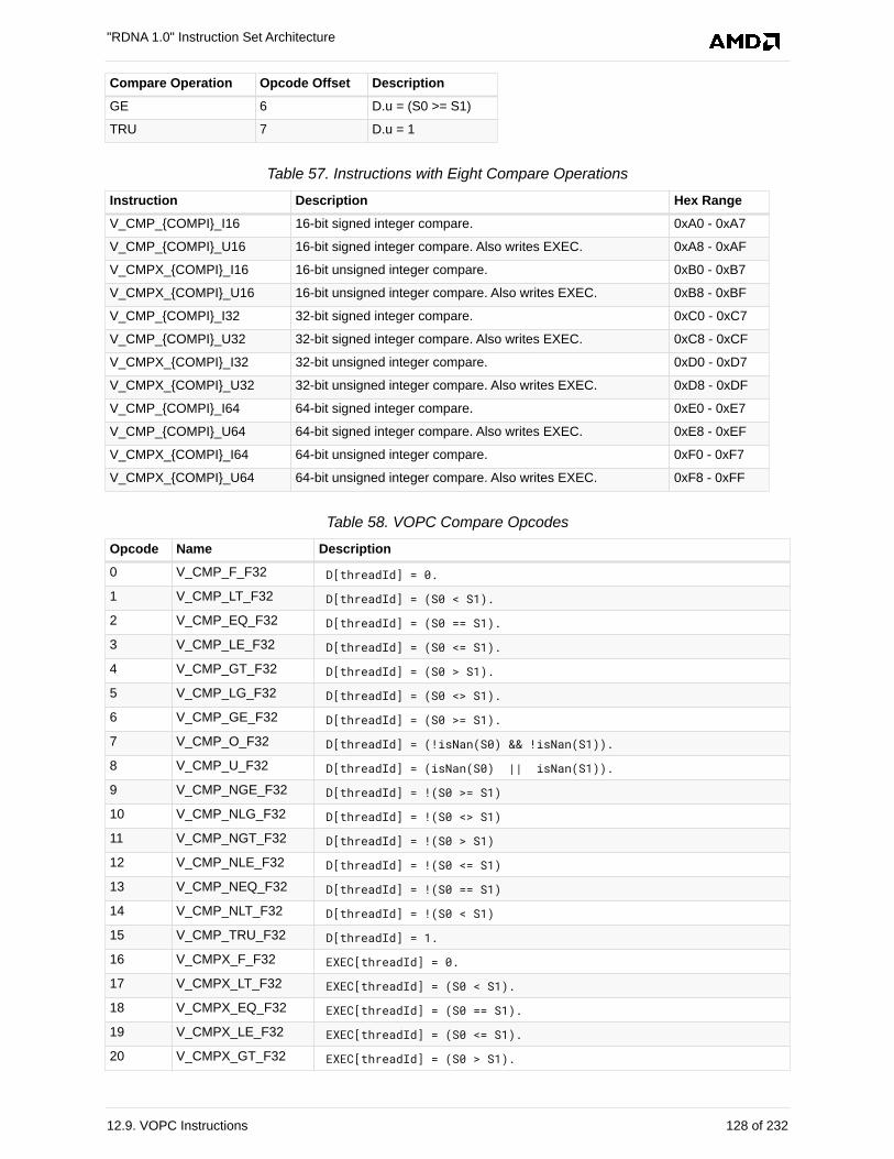
Compare Operation Opcode Offset Description
GE 6 D.u = (S0 >= S1)
TRU 7 D.u = 1
Table 57. Instructions with Eight Compare Operations
Instruction Description Hex Range
V_CMP_{COMPI}_I16 16-bit signed integer compare. 0xA0 - 0xA7
V_CMP_{COMPI}_U16 16-bit signed integer compare. Also writes EXEC. 0xA8 - 0xAF
V_CMPX_{COMPI}_I16 16-bit unsigned integer compare. 0xB0 - 0xB7
V_CMPX_{COMPI}_U16 16-bit unsigned integer compare. Also writes EXEC. 0xB8 - 0xBF
V_CMP_{COMPI}_I32 32-bit signed integer compare. 0xC0 - 0xC7
V_CMP_{COMPI}_U32 32-bit signed integer compare. Also writes EXEC. 0xC8 - 0xCF
V_CMPX_{COMPI}_I32 32-bit unsigned integer compare. 0xD0 - 0xD7
V_CMPX_{COMPI}_U32 32-bit unsigned integer compare. Also writes EXEC. 0xD8 - 0xDF
V_CMP_{COMPI}_I64 64-bit signed integer compare. 0xE0 - 0xE7
V_CMP_{COMPI}_U64 64-bit signed integer compare. Also writes EXEC. 0xE8 - 0xEF
V_CMPX_{COMPI}_I64 64-bit unsigned integer compare. 0xF0 - 0xF7
V_CMPX_{COMPI}_U64 64-bit unsigned integer compare. Also writes EXEC. 0xF8 - 0xFF
Table 58. VOPC Compare Opcodes
Opcode Name Description
0 V_CMP_F_F32 D[threadId] = 0.
1 V_CMP_LT_F32 D[threadId] = (S0 < S1).
2 V_CMP_EQ_F32 D[threadId] = (S0 == S1).
3 V_CMP_LE_F32 D[threadId] = (S0 <= S1).
4 V_CMP_GT_F32 D[threadId] = (S0 > S1).
5 V_CMP_LG_F32 D[threadId] = (S0 <> S1).
6 V_CMP_GE_F32 D[threadId] = (S0 >= S1).
7 V_CMP_O_F32 D[threadId] = (!isNan(S0) && !isNan(S1)).
8 V_CMP_U_F32 D[threadId] = (isNan(S0) || isNan(S1)).
9 V_CMP_NGE_F32 D[threadId] = !(S0 >= S1)
10 V_CMP_NLG_F32 D[threadId] = !(S0 <> S1)
11 V_CMP_NGT_F32 D[threadId] = !(S0 > S1)
12 V_CMP_NLE_F32 D[threadId] = !(S0 <= S1)
13 V_CMP_NEQ_F32 D[threadId] = !(S0 == S1)
14 V_CMP_NLT_F32 D[threadId] = !(S0 < S1)
15 V_CMP_TRU_F32 D[threadId] = 1.
16 V_CMPX_F_F32 EXEC[threadId] = 0.
17 V_CMPX_LT_F32 EXEC[threadId] = (S0 < S1).
18 V_CMPX_EQ_F32 EXEC[threadId] = (S0 == S1).
19 V_CMPX_LE_F32 EXEC[threadId] = (S0 <= S1).
20 V_CMPX_GT_F32 EXEC[threadId] = (S0 > S1).
"RDNA 1.0" Instruction Set Architecture
12.9. VOPC Instructions 128 of 232
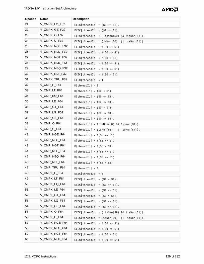
Opcode Name Description
21 V_CMPX_LG_F32 EXEC[threadId] = (S0 <> S1).
22 V_CMPX_GE_F32 EXEC[threadId] = (S0 >= S1).
23 V_CMPX_O_F32 EXEC[threadId] = (!isNan(S0) && !isNan(S1)).
24 V_CMPX_U_F32 EXEC[threadId] = (isNan(S0) || isNan(S1)).
25 V_CMPX_NGE_F32 EXEC[threadId] = !(S0 >= S1)
26 V_CMPX_NLG_F32 EXEC[threadId] = !(S0 <> S1)
27 V_CMPX_NGT_F32 EXEC[threadId] = !(S0 > S1)
28 V_CMPX_NLE_F32 EXEC[threadId] = !(S0 <= S1)
29 V_CMPX_NEQ_F32 EXEC[threadId] = !(S0 == S1)
30 V_CMPX_NLT_F32 EXEC[threadId] = !(S0 < S1)
31 V_CMPX_TRU_F32 EXEC[threadId] = 1.
32 V_CMP_F_F64 D[threadId] = 0.
33 V_CMP_LT_F64 D[threadId] = (S0 < S1).
34 V_CMP_EQ_F64 D[threadId] = (S0 == S1).
35 V_CMP_LE_F64 D[threadId] = (S0 <= S1).
36 V_CMP_GT_F64 D[threadId] = (S0 > S1).
37 V_CMP_LG_F64 D[threadId] = (S0 <> S1).
38 V_CMP_GE_F64 D[threadId] = (S0 >= S1).
39 V_CMP_O_F64 D[threadId] = (!isNan(S0) && !isNan(S1)).
40 V_CMP_U_F64 D[threadId] = (isNan(S0) || isNan(S1)).
41 V_CMP_NGE_F64 D[threadId] = !(S0 >= S1)
42 V_CMP_NLG_F64 D[threadId] = !(S0 <> S1)
43 V_CMP_NGT_F64 D[threadId] = !(S0 > S1)
44 V_CMP_NLE_F64 D[threadId] = !(S0 <= S1)
45 V_CMP_NEQ_F64 D[threadId] = !(S0 == S1)
46 V_CMP_NLT_F64 D[threadId] = !(S0 < S1)
47 V_CMP_TRU_F64 D[threadId] = 1.
48 V_CMPX_F_F64 EXEC[threadId] = 0.
49 V_CMPX_LT_F64 EXEC[threadId] = (S0 < S1).
50 V_CMPX_EQ_F64 EXEC[threadId] = (S0 == S1).
51 V_CMPX_LE_F64 EXEC[threadId] = (S0 <= S1).
52 V_CMPX_GT_F64 EXEC[threadId] = (S0 > S1).
53 V_CMPX_LG_F64 EXEC[threadId] = (S0 <> S1).
54 V_CMPX_GE_F64 EXEC[threadId] = (S0 >= S1).
55 V_CMPX_O_F64 EXEC[threadId] = (!isNan(S0) && !isNan(S1)).
56 V_CMPX_U_F64 EXEC[threadId] = (isNan(S0) || isNan(S1)).
57 V_CMPX_NGE_F64 EXEC[threadId] = !(S0 >= S1)
58 V_CMPX_NLG_F64 EXEC[threadId] = !(S0 <> S1)
59 V_CMPX_NGT_F64 EXEC[threadId] = !(S0 > S1)
60 V_CMPX_NLE_F64 EXEC[threadId] = !(S0 <= S1)
"RDNA 1.0" Instruction Set Architecture
12.9. VOPC Instructions 129 of 232
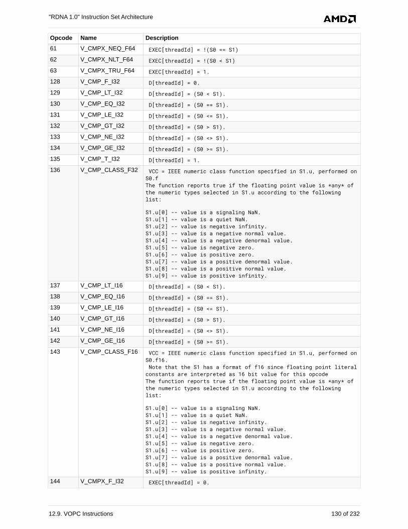
Opcode Name Description
61 V_CMPX_NEQ_F64 EXEC[threadId] = !(S0 == S1)
62 V_CMPX_NLT_F64 EXEC[threadId] = !(S0 < S1)
63 V_CMPX_TRU_F64 EXEC[threadId] = 1.
128 V_CMP_F_I32 D[threadId] = 0.
129 V_CMP_LT_I32 D[threadId] = (S0 < S1).
130 V_CMP_EQ_I32 D[threadId] = (S0 == S1).
131 V_CMP_LE_I32 D[threadId] = (S0 <= S1).
132 V_CMP_GT_I32 D[threadId] = (S0 > S1).
133 V_CMP_NE_I32 D[threadId] = (S0 <> S1).
134 V_CMP_GE_I32 D[threadId] = (S0 >= S1).
135 V_CMP_T_I32 D[threadId] = 1.
136 V_CMP_CLASS_F32 VCC = IEEE numeric class function specified in S1.u, performed onS0.fThe function reports true if the floating point value is *any* ofthe numeric types selected in S1.u according to the followinglist:
S1.u[0] -- value is a signaling NaN.S1.u[1] -- value is a quiet NaN.S1.u[2] -- value is negative infinity.S1.u[3] -- value is a negative normal value.S1.u[4] -- value is a negative denormal value.S1.u[5] -- value is negative zero.S1.u[6] -- value is positive zero.S1.u[7] -- value is a positive denormal value.S1.u[8] -- value is a positive normal value.S1.u[9] -- value is positive infinity.
137 V_CMP_LT_I16 D[threadId] = (S0 < S1).
138 V_CMP_EQ_I16 D[threadId] = (S0 == S1).
139 V_CMP_LE_I16 D[threadId] = (S0 <= S1).
140 V_CMP_GT_I16 D[threadId] = (S0 > S1).
141 V_CMP_NE_I16 D[threadId] = (S0 <> S1).
142 V_CMP_GE_I16 D[threadId] = (S0 >= S1).
143 V_CMP_CLASS_F16 VCC = IEEE numeric class function specified in S1.u, performed onS0.f16. Note that the S1 has a format of f16 since floating point literalconstants are interpreted as 16 bit value for this opcodeThe function reports true if the floating point value is *any* ofthe numeric types selected in S1.u according to the followinglist:
S1.u[0] -- value is a signaling NaN.S1.u[1] -- value is a quiet NaN.S1.u[2] -- value is negative infinity.S1.u[3] -- value is a negative normal value.S1.u[4] -- value is a negative denormal value.S1.u[5] -- value is negative zero.S1.u[6] -- value is positive zero.S1.u[7] -- value is a positive denormal value.S1.u[8] -- value is a positive normal value.S1.u[9] -- value is positive infinity.
144 V_CMPX_F_I32 EXEC[threadId] = 0.
"RDNA 1.0" Instruction Set Architecture
12.9. VOPC Instructions 130 of 232
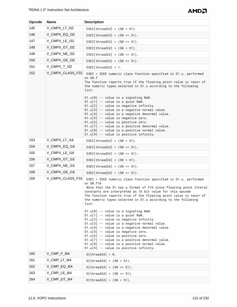
Opcode Name Description
145 V_CMPX_LT_I32 EXEC[threadId] = (S0 < S1).
146 V_CMPX_EQ_I32 EXEC[threadId] = (S0 == S1).
147 V_CMPX_LE_I32 EXEC[threadId] = (S0 <= S1).
148 V_CMPX_GT_I32 EXEC[threadId] = (S0 > S1).
149 V_CMPX_NE_I32 EXEC[threadId] = (S0 <> S1).
150 V_CMPX_GE_I32 EXEC[threadId] = (S0 >= S1).
151 V_CMPX_T_I32 EXEC[threadId] = 1.
152 V_CMPX_CLASS_F32 EXEC = IEEE numeric class function specified in S1.u, performedon S0.fThe function reports true if the floating point value is *any* ofthe numeric types selected in S1.u according to the followinglist:
S1.u[0] -- value is a signaling NaN.S1.u[1] -- value is a quiet NaN.S1.u[2] -- value is negative infinity.S1.u[3] -- value is a negative normal value.S1.u[4] -- value is a negative denormal value.S1.u[5] -- value is negative zero.S1.u[6] -- value is positive zero.S1.u[7] -- value is a positive denormal value.S1.u[8] -- value is a positive normal value.S1.u[9] -- value is positive infinity.
153 V_CMPX_LT_I16 EXEC[threadId] = (S0 < S1).
154 V_CMPX_EQ_I16 EXEC[threadId] = (S0 == S1).
155 V_CMPX_LE_I16 EXEC[threadId] = (S0 <= S1).
156 V_CMPX_GT_I16 EXEC[threadId] = (S0 > S1).
157 V_CMPX_NE_I16 EXEC[threadId] = (S0 <> S1).
158 V_CMPX_GE_I16 EXEC[threadId] = (S0 >= S1).
159 V_CMPX_CLASS_F16 EXEC = IEEE numeric class function specified in S1.u, performedon S0.f16 Note that the S1 has a format of f16 since floating point literalconstants are interpreted as 16 bit value for this opcodeThe function reports true if the floating point value is *any* ofthe numeric types selected in S1.u according to the followinglist:
S1.u[0] -- value is a signaling NaN.S1.u[1] -- value is a quiet NaN.S1.u[2] -- value is negative infinity.S1.u[3] -- value is a negative normal value.S1.u[4] -- value is a negative denormal value.S1.u[5] -- value is negative zero.S1.u[6] -- value is positive zero.S1.u[7] -- value is a positive denormal value.S1.u[8] -- value is a positive normal value.S1.u[9] -- value is positive infinity.
160 V_CMP_F_I64 D[threadId] = 0.
161 V_CMP_LT_I64 D[threadId] = (S0 < S1).
162 V_CMP_EQ_I64 D[threadId] = (S0 == S1).
163 V_CMP_LE_I64 D[threadId] = (S0 <= S1).
164 V_CMP_GT_I64 D[threadId] = (S0 > S1).
"RDNA 1.0" Instruction Set Architecture
12.9. VOPC Instructions 131 of 232
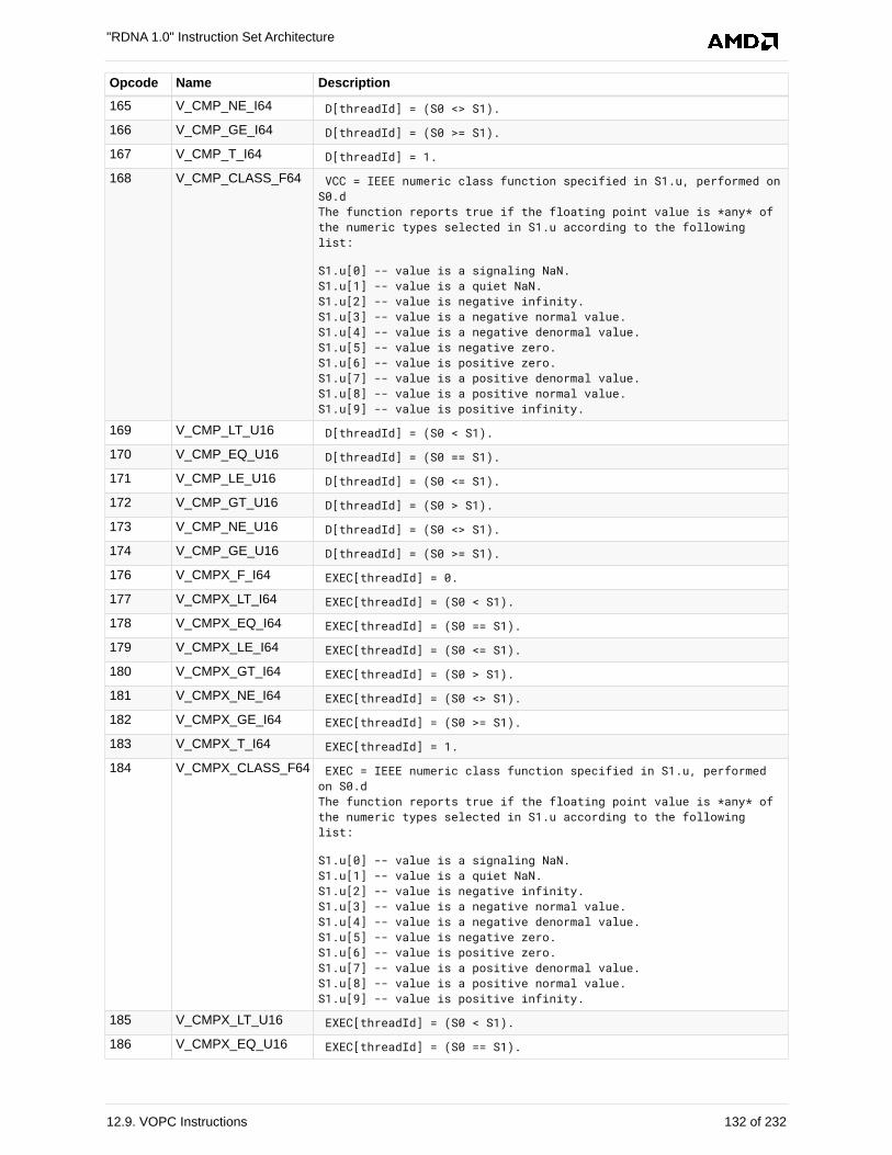
Opcode Name Description
165 V_CMP_NE_I64 D[threadId] = (S0 <> S1).
166 V_CMP_GE_I64 D[threadId] = (S0 >= S1).
167 V_CMP_T_I64 D[threadId] = 1.
168 V_CMP_CLASS_F64 VCC = IEEE numeric class function specified in S1.u, performed onS0.dThe function reports true if the floating point value is *any* ofthe numeric types selected in S1.u according to the followinglist:
S1.u[0] -- value is a signaling NaN.S1.u[1] -- value is a quiet NaN.S1.u[2] -- value is negative infinity.S1.u[3] -- value is a negative normal value.S1.u[4] -- value is a negative denormal value.S1.u[5] -- value is negative zero.S1.u[6] -- value is positive zero.S1.u[7] -- value is a positive denormal value.S1.u[8] -- value is a positive normal value.S1.u[9] -- value is positive infinity.
169 V_CMP_LT_U16 D[threadId] = (S0 < S1).
170 V_CMP_EQ_U16 D[threadId] = (S0 == S1).
171 V_CMP_LE_U16 D[threadId] = (S0 <= S1).
172 V_CMP_GT_U16 D[threadId] = (S0 > S1).
173 V_CMP_NE_U16 D[threadId] = (S0 <> S1).
174 V_CMP_GE_U16 D[threadId] = (S0 >= S1).
176 V_CMPX_F_I64 EXEC[threadId] = 0.
177 V_CMPX_LT_I64 EXEC[threadId] = (S0 < S1).
178 V_CMPX_EQ_I64 EXEC[threadId] = (S0 == S1).
179 V_CMPX_LE_I64 EXEC[threadId] = (S0 <= S1).
180 V_CMPX_GT_I64 EXEC[threadId] = (S0 > S1).
181 V_CMPX_NE_I64 EXEC[threadId] = (S0 <> S1).
182 V_CMPX_GE_I64 EXEC[threadId] = (S0 >= S1).
183 V_CMPX_T_I64 EXEC[threadId] = 1.
184 V_CMPX_CLASS_F64 EXEC = IEEE numeric class function specified in S1.u, performedon S0.dThe function reports true if the floating point value is *any* ofthe numeric types selected in S1.u according to the followinglist:
S1.u[0] -- value is a signaling NaN.S1.u[1] -- value is a quiet NaN.S1.u[2] -- value is negative infinity.S1.u[3] -- value is a negative normal value.S1.u[4] -- value is a negative denormal value.S1.u[5] -- value is negative zero.S1.u[6] -- value is positive zero.S1.u[7] -- value is a positive denormal value.S1.u[8] -- value is a positive normal value.S1.u[9] -- value is positive infinity.
185 V_CMPX_LT_U16 EXEC[threadId] = (S0 < S1).
186 V_CMPX_EQ_U16 EXEC[threadId] = (S0 == S1).
"RDNA 1.0" Instruction Set Architecture
12.9. VOPC Instructions 132 of 232
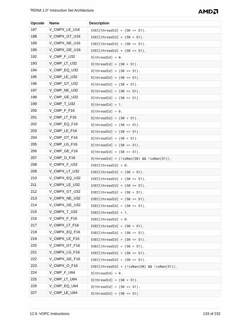
Opcode Name Description
187 V_CMPX_LE_U16 EXEC[threadId] = (S0 <= S1).
188 V_CMPX_GT_U16 EXEC[threadId] = (S0 > S1).
189 V_CMPX_NE_U16 EXEC[threadId] = (S0 <> S1).
190 V_CMPX_GE_U16 EXEC[threadId] = (S0 >= S1).
192 V_CMP_F_U32 D[threadId] = 0.
193 V_CMP_LT_U32 D[threadId] = (S0 < S1).
194 V_CMP_EQ_U32 D[threadId] = (S0 == S1).
195 V_CMP_LE_U32 D[threadId] = (S0 <= S1).
196 V_CMP_GT_U32 D[threadId] = (S0 > S1).
197 V_CMP_NE_U32 D[threadId] = (S0 <> S1).
198 V_CMP_GE_U32 D[threadId] = (S0 >= S1).
199 V_CMP_T_U32 D[threadId] = 1.
200 V_CMP_F_F16 D[threadId] = 0.
201 V_CMP_LT_F16 D[threadId] = (S0 < S1).
202 V_CMP_EQ_F16 D[threadId] = (S0 == S1).
203 V_CMP_LE_F16 D[threadId] = (S0 <= S1).
204 V_CMP_GT_F16 D[threadId] = (S0 > S1).
205 V_CMP_LG_F16 D[threadId] = (S0 <> S1).
206 V_CMP_GE_F16 D[threadId] = (S0 >= S1).
207 V_CMP_O_F16 D[threadId] = (!isNan(S0) && !isNan(S1)).
208 V_CMPX_F_U32 EXEC[threadId] = 0.
209 V_CMPX_LT_U32 EXEC[threadId] = (S0 < S1).
210 V_CMPX_EQ_U32 EXEC[threadId] = (S0 == S1).
211 V_CMPX_LE_U32 EXEC[threadId] = (S0 <= S1).
212 V_CMPX_GT_U32 EXEC[threadId] = (S0 > S1).
213 V_CMPX_NE_U32 EXEC[threadId] = (S0 <> S1).
214 V_CMPX_GE_U32 EXEC[threadId] = (S0 >= S1).
215 V_CMPX_T_U32 EXEC[threadId] = 1.
216 V_CMPX_F_F16 EXEC[threadId] = 0.
217 V_CMPX_LT_F16 EXEC[threadId] = (S0 < S1).
218 V_CMPX_EQ_F16 EXEC[threadId] = (S0 == S1).
219 V_CMPX_LE_F16 EXEC[threadId] = (S0 <= S1).
220 V_CMPX_GT_F16 EXEC[threadId] = (S0 > S1).
221 V_CMPX_LG_F16 EXEC[threadId] = (S0 <> S1).
222 V_CMPX_GE_F16 EXEC[threadId] = (S0 >= S1).
223 V_CMPX_O_F16 EXEC[threadId] = (!isNan(S0) && !isNan(S1)).
224 V_CMP_F_U64 D[threadId] = 0.
225 V_CMP_LT_U64 D[threadId] = (S0 < S1).
226 V_CMP_EQ_U64 D[threadId] = (S0 == S1).
227 V_CMP_LE_U64 D[threadId] = (S0 <= S1).
"RDNA 1.0" Instruction Set Architecture
12.9. VOPC Instructions 133 of 232
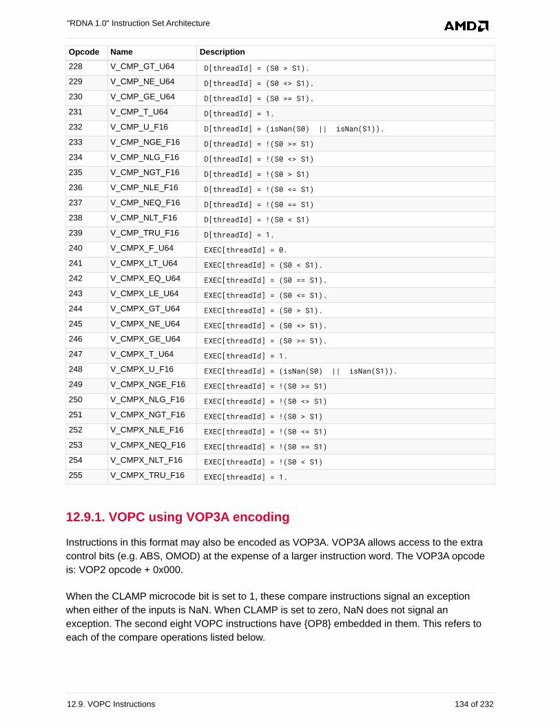
Opcode Name Description
228 V_CMP_GT_U64 D[threadId] = (S0 > S1).
229 V_CMP_NE_U64 D[threadId] = (S0 <> S1).
230 V_CMP_GE_U64 D[threadId] = (S0 >= S1).
231 V_CMP_T_U64 D[threadId] = 1.
232 V_CMP_U_F16 D[threadId] = (isNan(S0) || isNan(S1)).
233 V_CMP_NGE_F16 D[threadId] = !(S0 >= S1)
234 V_CMP_NLG_F16 D[threadId] = !(S0 <> S1)
235 V_CMP_NGT_F16 D[threadId] = !(S0 > S1)
236 V_CMP_NLE_F16 D[threadId] = !(S0 <= S1)
237 V_CMP_NEQ_F16 D[threadId] = !(S0 == S1)
238 V_CMP_NLT_F16 D[threadId] = !(S0 < S1)
239 V_CMP_TRU_F16 D[threadId] = 1.
240 V_CMPX_F_U64 EXEC[threadId] = 0.
241 V_CMPX_LT_U64 EXEC[threadId] = (S0 < S1).
242 V_CMPX_EQ_U64 EXEC[threadId] = (S0 == S1).
243 V_CMPX_LE_U64 EXEC[threadId] = (S0 <= S1).
244 V_CMPX_GT_U64 EXEC[threadId] = (S0 > S1).
245 V_CMPX_NE_U64 EXEC[threadId] = (S0 <> S1).
246 V_CMPX_GE_U64 EXEC[threadId] = (S0 >= S1).
247 V_CMPX_T_U64 EXEC[threadId] = 1.
248 V_CMPX_U_F16 EXEC[threadId] = (isNan(S0) || isNan(S1)).
249 V_CMPX_NGE_F16 EXEC[threadId] = !(S0 >= S1)
250 V_CMPX_NLG_F16 EXEC[threadId] = !(S0 <> S1)
251 V_CMPX_NGT_F16 EXEC[threadId] = !(S0 > S1)
252 V_CMPX_NLE_F16 EXEC[threadId] = !(S0 <= S1)
253 V_CMPX_NEQ_F16 EXEC[threadId] = !(S0 == S1)
254 V_CMPX_NLT_F16 EXEC[threadId] = !(S0 < S1)
255 V_CMPX_TRU_F16 EXEC[threadId] = 1.
12.9.1. VOPC using VOP3A encoding
Instructions in this format may also be encoded as VOP3A. VOP3A allows access to the extra
control bits (e.g. ABS, OMOD) at the expense of a larger instruction word. The VOP3A opcode
is: VOP2 opcode + 0x000.
When the CLAMP microcode bit is set to 1, these compare instructions signal an exception
when either of the inputs is NaN. When CLAMP is set to zero, NaN does not signal an
exception. The second eight VOPC instructions have {OP8} embedded in them. This refers to
each of the compare operations listed below.
"RDNA 1.0" Instruction Set Architecture
12.9. VOPC Instructions 134 of 232
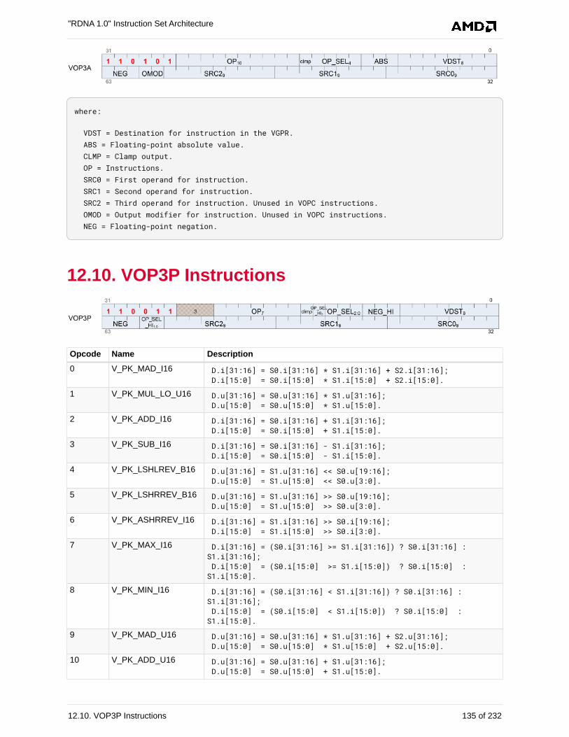
where:
VDST = Destination for instruction in the VGPR. ABS = Floating-point absolute value. CLMP = Clamp output. OP = Instructions. SRC0 = First operand for instruction. SRC1 = Second operand for instruction. SRC2 = Third operand for instruction. Unused in VOPC instructions. OMOD = Output modifier for instruction. Unused in VOPC instructions. NEG = Floating-point negation.
12.10. VOP3P Instructions
Opcode Name Description
0 V_PK_MAD_I16 D.i[31:16] = S0.i[31:16] * S1.i[31:16] + S2.i[31:16]; D.i[15:0] = S0.i[15:0] * S1.i[15:0] + S2.i[15:0].
1 V_PK_MUL_LO_U16 D.u[31:16] = S0.u[31:16] * S1.u[31:16]; D.u[15:0] = S0.u[15:0] * S1.u[15:0].
2 V_PK_ADD_I16 D.i[31:16] = S0.i[31:16] + S1.i[31:16]; D.i[15:0] = S0.i[15:0] + S1.i[15:0].
3 V_PK_SUB_I16 D.i[31:16] = S0.i[31:16] - S1.i[31:16]; D.i[15:0] = S0.i[15:0] - S1.i[15:0].
4 V_PK_LSHLREV_B16 D.u[31:16] = S1.u[31:16] << S0.u[19:16]; D.u[15:0] = S1.u[15:0] << S0.u[3:0].
5 V_PK_LSHRREV_B16 D.u[31:16] = S1.u[31:16] >> S0.u[19:16]; D.u[15:0] = S1.u[15:0] >> S0.u[3:0].
6 V_PK_ASHRREV_I16 D.i[31:16] = S1.i[31:16] >> S0.i[19:16]; D.i[15:0] = S1.i[15:0] >> S0.i[3:0].
7 V_PK_MAX_I16 D.i[31:16] = (S0.i[31:16] >= S1.i[31:16]) ? S0.i[31:16] :S1.i[31:16]; D.i[15:0] = (S0.i[15:0] >= S1.i[15:0]) ? S0.i[15:0] :S1.i[15:0].
8 V_PK_MIN_I16 D.i[31:16] = (S0.i[31:16] < S1.i[31:16]) ? S0.i[31:16] :S1.i[31:16]; D.i[15:0] = (S0.i[15:0] < S1.i[15:0]) ? S0.i[15:0] :S1.i[15:0].
9 V_PK_MAD_U16 D.u[31:16] = S0.u[31:16] * S1.u[31:16] + S2.u[31:16]; D.u[15:0] = S0.u[15:0] * S1.u[15:0] + S2.u[15:0].
10 V_PK_ADD_U16 D.u[31:16] = S0.u[31:16] + S1.u[31:16]; D.u[15:0] = S0.u[15:0] + S1.u[15:0].
"RDNA 1.0" Instruction Set Architecture
12.10. VOP3P Instructions 135 of 232
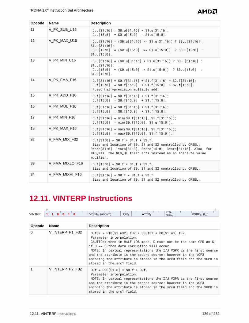
Opcode Name Description
11 V_PK_SUB_U16 D.u[31:16] = S0.u[31:16] - S1.u[31:16]; D.u[15:0] = S0.u[15:0] - S1.u[15:0].
12 V_PK_MAX_U16 D.u[31:16] = (S0.u[31:16] >= S1.u[31:16]) ? S0.u[31:16] :S1.u[31:16]; D.u[15:0] = (S0.u[15:0] >= S1.u[15:0]) ? S0.u[15:0] :S1.u[15:0].
13 V_PK_MIN_U16 D.u[31:16] = (S0.u[31:16] < S1.u[31:16]) ? S0.u[31:16] :S1.u[31:16]; D.u[15:0] = (S0.u[15:0] < S1.u[15:0]) ? S0.u[15:0] :S1.u[15:0].
14 V_PK_FMA_F16 D.f[31:16] = S0.f[31:16] * S1.f[31:16] + S2.f[31:16]; D.f[15:0] = S0.f[15:0] * S1.f[15:0] + S2.f[15:0]. Fused half-precision multiply add.
15 V_PK_ADD_F16 D.f[31:16] = S0.f[31:16] + S1.f[31:16]; D.f[15:0] = S0.f[15:0] + S1.f[15:0].
16 V_PK_MUL_F16 D.f[31:16] = S0.f[31:16] * S1.f[31:16]; D.f[15:0] = S0.f[15:0] * S1.f[15:0].
17 V_PK_MIN_F16 D.f[31:16] = min(S0.f[31:16], S1.f[31:16]); D.f[15:0] = min(S0.f[15:0], S1.u[15:0]).
18 V_PK_MAX_F16 D.f[31:16] = max(S0.f[31:16], S1.f[31:16]); D.f[15:0] = max(S0.f[15:0], S1.f[15:0]).
32 V_FMA_MIX_F32 D.f[31:0] = S0.f * S1.f + S2.f. Size and location of S0, S1 and S2 controlled by OPSEL:0=src[31:0], 1=src[31:0], 2=src[15:0], 3=src[31:16]. Also, forMAD_MIX, the NEG_HI field acts instead as an absolute-valuemodifier.
33 V_FMA_MIXLO_F16 D.f[15:0] = S0.f * S1.f + S2.f. Size and location of S0, S1 and S2 controlled by OPSEL.
34 V_FMA_MIXHI_F16 D.f[31:16] = S0.f * S1.f + S2.f. Size and location of S0, S1 and S2 controlled by OPSEL.
12.11. VINTERP Instructions
Opcode Name Description
0 V_INTERP_P1_F32 D.f32 = P10[S1.u32].f32 * S0.f32 + P0[S1.u3].f32. Parameter interpolation. CAUTION: when in HALF_LDS mode, D must not be the same GPR as S;if D == S then data corruption will occur. NOTE: In textual representations the I/J VGPR is the first sourceand the attribute is the second source; however in the VOP3encoding the attribute is stored in the src0 field and the VGPR isstored in the src1 field.
1 V_INTERP_P2_F32 D.f = P20[S1.u] * S0.f + D.f. Parameter interpolation. NOTE: In textual representations the I/J VGPR is the first sourceand the attribute is the second source; however in the VOP3encoding the attribute is stored in the src0 field and the VGPR isstored in the src1 field.
"RDNA 1.0" Instruction Set Architecture
12.11. VINTERP Instructions 136 of 232
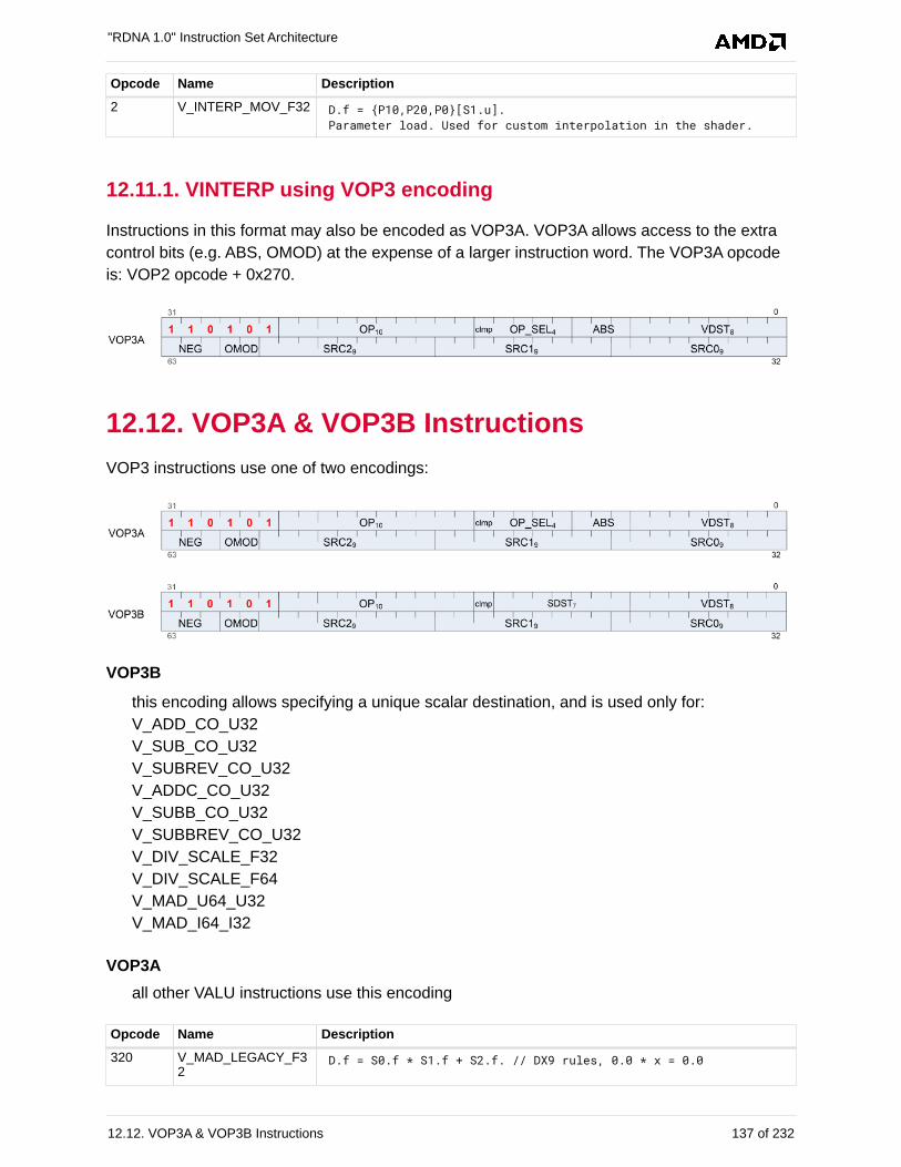
Opcode Name Description
2 V_INTERP_MOV_F32 D.f = {P10,P20,P0}[S1.u]. Parameter load. Used for custom interpolation in the shader.
12.11.1. VINTERP using VOP3 encoding
Instructions in this format may also be encoded as VOP3A. VOP3A allows access to the extra
control bits (e.g. ABS, OMOD) at the expense of a larger instruction word. The VOP3A opcode
is: VOP2 opcode + 0x270.
12.12. VOP3A & VOP3B Instructions
VOP3 instructions use one of two encodings:
VOP3B
this encoding allows specifying a unique scalar destination, and is used only for:
V_ADD_CO_U32
V_SUB_CO_U32
V_SUBREV_CO_U32
V_ADDC_CO_U32
V_SUBB_CO_U32
V_SUBBREV_CO_U32
V_DIV_SCALE_F32
V_DIV_SCALE_F64
V_MAD_U64_U32
V_MAD_I64_I32
VOP3A
all other VALU instructions use this encoding
Opcode Name Description
320 V_MAD_LEGACY_F32
D.f = S0.f * S1.f + S2.f. // DX9 rules, 0.0 * x = 0.0
"RDNA 1.0" Instruction Set Architecture
12.12. VOP3A & VOP3B Instructions 137 of 232
Opcode Name Description
321 V_MAD_F32 D.f = S0.f * S1.f + S2.f. 1ULP accuracy, denormals are flushed.
322 V_MAD_I32_I24 D.i = S0.i[23:0] * S1.i[23:0] + S2.i.
323 V_MAD_U32_U24 D.u = S0.u[23:0] * S1.u[23:0] + S2.u.
324 V_CUBEID_F32 // Set D.f = cubemap face ID ({0.0, 1.0, ..., 5.0}). // XYZ coordinate is given in (S0.f, S1.f, S2.f). // S0.f = x // S1.f = y // S2.f = z if (abs(S2.f) >= abs(S0.f) && abs(S2.f) >= abs(S1.f)) if (S2.f < 0) D.f = 5.0; else D.f = 4.0; endif; else if (abs(S1.f) >= abs(S0.f)) if (S1.f < 0) D.f = 3.0; else D.f = 2.0; endif; else if (S0.f < 0) D.f = 1.0; else D.f = 0.0; endif; endif. Cubemap Face ID determination. Result is a floating point faceID.
325 V_CUBESC_F32 // D.f = cubemap S coordinate. // XYZ coordinate is given in (S0.f, S1.f, S2.f). // S0.f = x // S1.f = y // S2.f = z if (abs(S2.f) >= abs(S0.f) && abs(S2.f) >= abs(S1.f)) if (S2.f < 0) D.f = -S0.f; else D.f = S0.f; endif; else if (abs(S1.f) >= abs(S0.f)) D.f = S0.f; else if (S0.f < 0) D.f = S2.f; else D.f = -S2.f; endif; endif. Cubemap S coordinate.
"RDNA 1.0" Instruction Set Architecture
12.12. VOP3A & VOP3B Instructions 138 of 232
Opcode Name Description
326 V_CUBETC_F32 // D.f = cubemap T coordinate. // XYZ coordinate is given in (S0.f, S1.f, S2.f). // S0.f = x // S1.f = y // S2.f = z if (abs(S2.f) >= abs(S0.f) && abs(S2.f) >= bs(S1.f)) D.f = -S1.f; else if (abs(S1.f) >= abs(S0.f)) if (S1.f < 0) D.f = -S2.f; else D.f = S2.f; endif; else D.f = -S1.f; endif. Cubemap T coordinate.
327 V_CUBEMA_F32 // D.f = 2.0 * cubemap major axis. // XYZ coordinate is given in (S0.f, S1.f, S2.f). // S0.f = x // S1.f = y // S2.f = z if (abs(S2.f) >= abs(S0.f) && abs(S2.f) >= abs(S1.f)) D.f = 2.0 * S2.f; else if (abs(S1.f) >= abs(S0.f)) D.f = 2.0 * S1.f; else D.f = 2.0 * S0.f; endif. Determine cubemap major axis.
328 V_BFE_U32 D.u = (S0.u >> S1.u[4:0]) & ((1 << S2.u[4:0]) - 1). Bitfield extract with S0 = data, S1 = field_offset, S2 =field_width.
329 V_BFE_I32 D.i = (S0.i >> S1.u[4:0]) & ((1 << S2.u[4:0]) - 1). Bitfield extract with S0 = data, S1 = field_offset, S2 =field_width.
330 V_BFI_B32 D.u = (S0.u & S1.u) | (~S0.u & S2.u). Bitfield insert.
331 V_FMA_F32 D.f = S0.f * S1.f + S2.f. Fused single precision multiply add. 0.5ULP accuracy, denormalsare supported.
332 V_FMA_F64 D.d = S0.d * S1.d + S2.d. Fused double precision multiply add. 0.5ULP precision, denormalsare supported.
333 V_LERP_U8 D.u = ((S0.u[31:24] + S1.u[31:24] + S2.u[24]) >> 1) << 24 D.u += ((S0.u[23:16] + S1.u[23:16] + S2.u[16]) >> 1) << 16; D.u += ((S0.u[15:8] + S1.u[15:8] + S2.u[8]) >> 1) << 8; D.u += ((S0.u[7:0] + S1.u[7:0] + S2.u[0]) >> 1). Unsigned 8-bit pixel average on packed unsigned bytes (linearinterpolation). S2 acts as a round mode; if set, 0.5 rounds up,otherwise 0.5 truncates.
334 V_ALIGNBIT_B32 D.u = ({S0,S1} >> S2.u[4:0]) & 0xffffffff.
335 V_ALIGNBYTE_B32 D.u = ({S0,S1} >> (8*S2.u[4:0])) & 0xffffffff.
336 V_MULLIT_F32 D.f = S0.f * S1.f, replicate result into 4 components (0.0 * x = 0.0; special INF, NaN, overflow rules).
337 V_MIN3_F32 D.f = V_MIN_F32(V_MIN_F32(S0.f, S1.f), S2.f).
"RDNA 1.0" Instruction Set Architecture
12.12. VOP3A & VOP3B Instructions 139 of 232
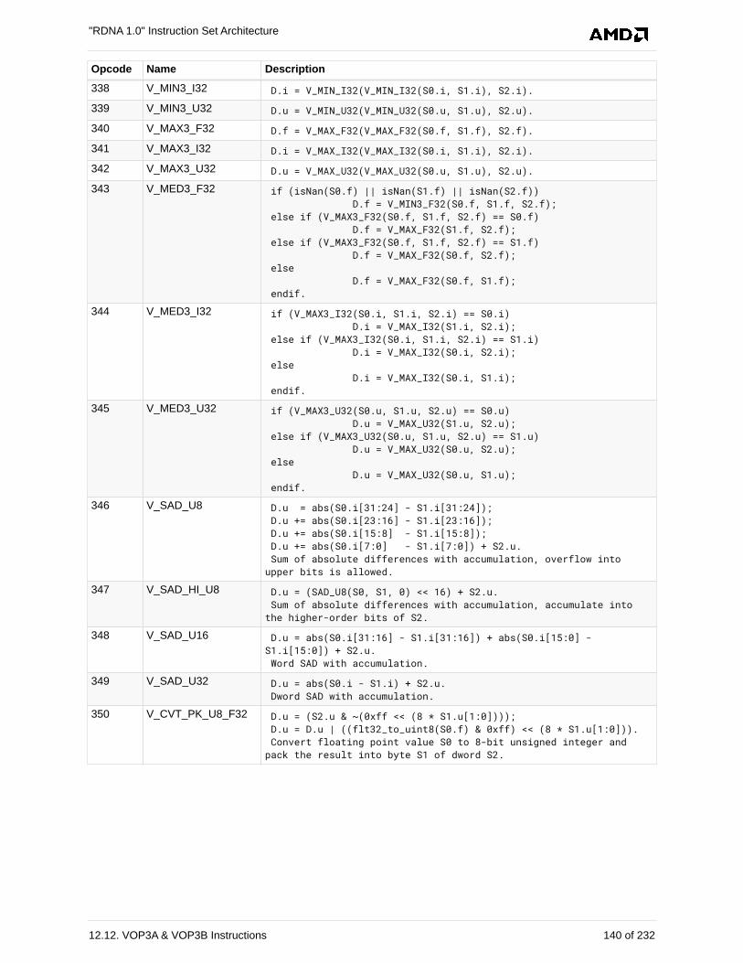
Opcode Name Description
338 V_MIN3_I32 D.i = V_MIN_I32(V_MIN_I32(S0.i, S1.i), S2.i).
339 V_MIN3_U32 D.u = V_MIN_U32(V_MIN_U32(S0.u, S1.u), S2.u).
340 V_MAX3_F32 D.f = V_MAX_F32(V_MAX_F32(S0.f, S1.f), S2.f).
341 V_MAX3_I32 D.i = V_MAX_I32(V_MAX_I32(S0.i, S1.i), S2.i).
342 V_MAX3_U32 D.u = V_MAX_U32(V_MAX_U32(S0.u, S1.u), S2.u).
343 V_MED3_F32 if (isNan(S0.f) || isNan(S1.f) || isNan(S2.f)) D.f = V_MIN3_F32(S0.f, S1.f, S2.f); else if (V_MAX3_F32(S0.f, S1.f, S2.f) == S0.f) D.f = V_MAX_F32(S1.f, S2.f); else if (V_MAX3_F32(S0.f, S1.f, S2.f) == S1.f) D.f = V_MAX_F32(S0.f, S2.f); else D.f = V_MAX_F32(S0.f, S1.f); endif.
344 V_MED3_I32 if (V_MAX3_I32(S0.i, S1.i, S2.i) == S0.i) D.i = V_MAX_I32(S1.i, S2.i); else if (V_MAX3_I32(S0.i, S1.i, S2.i) == S1.i) D.i = V_MAX_I32(S0.i, S2.i); else D.i = V_MAX_I32(S0.i, S1.i); endif.
345 V_MED3_U32 if (V_MAX3_U32(S0.u, S1.u, S2.u) == S0.u) D.u = V_MAX_U32(S1.u, S2.u); else if (V_MAX3_U32(S0.u, S1.u, S2.u) == S1.u) D.u = V_MAX_U32(S0.u, S2.u); else D.u = V_MAX_U32(S0.u, S1.u); endif.
346 V_SAD_U8 D.u = abs(S0.i[31:24] - S1.i[31:24]); D.u += abs(S0.i[23:16] - S1.i[23:16]); D.u += abs(S0.i[15:8] - S1.i[15:8]); D.u += abs(S0.i[7:0] - S1.i[7:0]) + S2.u. Sum of absolute differences with accumulation, overflow intoupper bits is allowed.
347 V_SAD_HI_U8 D.u = (SAD_U8(S0, S1, 0) << 16) + S2.u. Sum of absolute differences with accumulation, accumulate intothe higher-order bits of S2.
348 V_SAD_U16 D.u = abs(S0.i[31:16] - S1.i[31:16]) + abs(S0.i[15:0] -S1.i[15:0]) + S2.u. Word SAD with accumulation.
349 V_SAD_U32 D.u = abs(S0.i - S1.i) + S2.u. Dword SAD with accumulation.
350 V_CVT_PK_U8_F32 D.u = (S2.u & ~(0xff << (8 * S1.u[1:0]))); D.u = D.u | ((flt32_to_uint8(S0.f) & 0xff) << (8 * S1.u[1:0])). Convert floating point value S0 to 8-bit unsigned integer andpack the result into byte S1 of dword S2.
"RDNA 1.0" Instruction Set Architecture
12.12. VOP3A & VOP3B Instructions 140 of 232
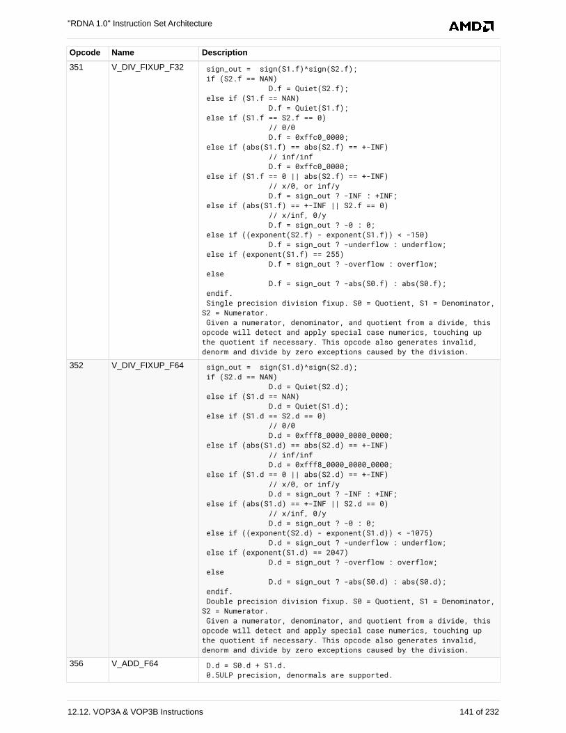
Opcode Name Description
351 V_DIV_FIXUP_F32 sign_out = sign(S1.f)^sign(S2.f); if (S2.f == NAN) D.f = Quiet(S2.f); else if (S1.f == NAN) D.f = Quiet(S1.f); else if (S1.f == S2.f == 0) // 0/0 D.f = 0xffc0_0000; else if (abs(S1.f) == abs(S2.f) == +-INF) // inf/inf D.f = 0xffc0_0000; else if (S1.f == 0 || abs(S2.f) == +-INF) // x/0, or inf/y D.f = sign_out ? -INF : +INF; else if (abs(S1.f) == +-INF || S2.f == 0) // x/inf, 0/y D.f = sign_out ? -0 : 0; else if ((exponent(S2.f) - exponent(S1.f)) < -150) D.f = sign_out ? -underflow : underflow; else if (exponent(S1.f) == 255) D.f = sign_out ? -overflow : overflow; else D.f = sign_out ? -abs(S0.f) : abs(S0.f); endif. Single precision division fixup. S0 = Quotient, S1 = Denominator,S2 = Numerator. Given a numerator, denominator, and quotient from a divide, thisopcode will detect and apply special case numerics, touching upthe quotient if necessary. This opcode also generates invalid,denorm and divide by zero exceptions caused by the division.
352 V_DIV_FIXUP_F64 sign_out = sign(S1.d)^sign(S2.d); if (S2.d == NAN) D.d = Quiet(S2.d); else if (S1.d == NAN) D.d = Quiet(S1.d); else if (S1.d == S2.d == 0) // 0/0 D.d = 0xfff8_0000_0000_0000; else if (abs(S1.d) == abs(S2.d) == +-INF) // inf/inf D.d = 0xfff8_0000_0000_0000; else if (S1.d == 0 || abs(S2.d) == +-INF) // x/0, or inf/y D.d = sign_out ? -INF : +INF; else if (abs(S1.d) == +-INF || S2.d == 0) // x/inf, 0/y D.d = sign_out ? -0 : 0; else if ((exponent(S2.d) - exponent(S1.d)) < -1075) D.d = sign_out ? -underflow : underflow; else if (exponent(S1.d) == 2047) D.d = sign_out ? -overflow : overflow; else D.d = sign_out ? -abs(S0.d) : abs(S0.d); endif. Double precision division fixup. S0 = Quotient, S1 = Denominator,S2 = Numerator. Given a numerator, denominator, and quotient from a divide, thisopcode will detect and apply special case numerics, touching upthe quotient if necessary. This opcode also generates invalid,denorm and divide by zero exceptions caused by the division.
356 V_ADD_F64 D.d = S0.d + S1.d. 0.5ULP precision, denormals are supported.
"RDNA 1.0" Instruction Set Architecture
12.12. VOP3A & VOP3B Instructions 141 of 232
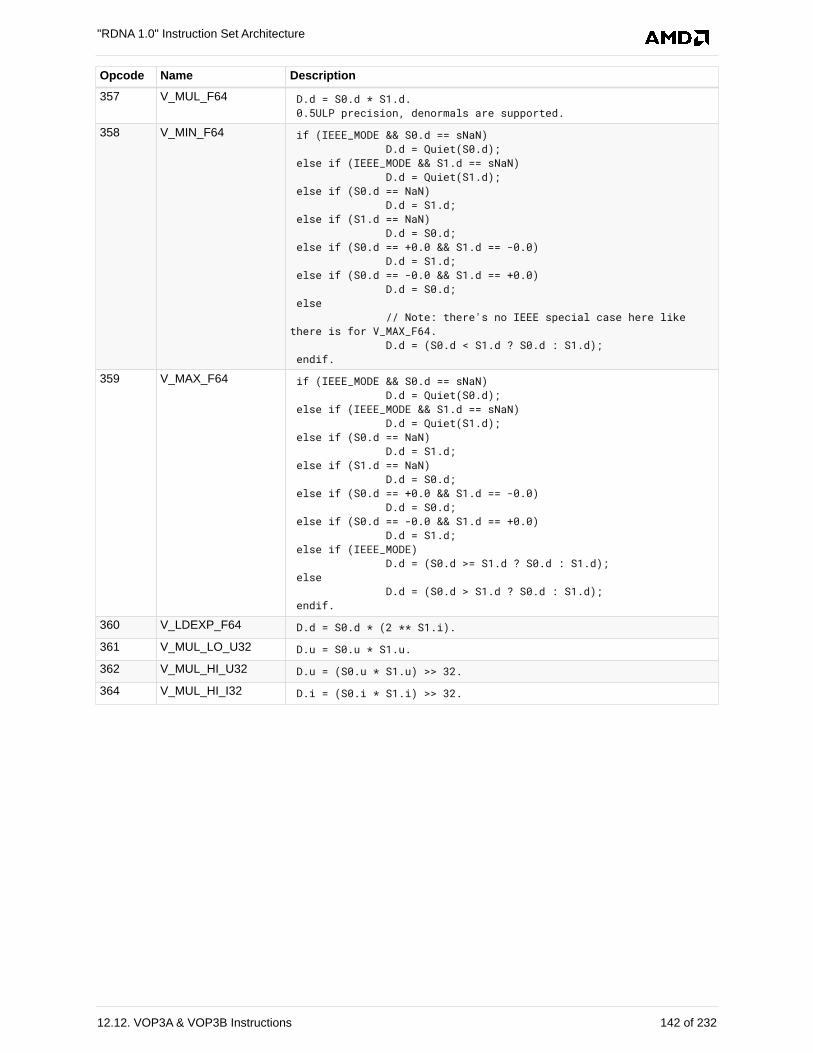
Opcode Name Description
357 V_MUL_F64 D.d = S0.d * S1.d. 0.5ULP precision, denormals are supported.
358 V_MIN_F64 if (IEEE_MODE && S0.d == sNaN) D.d = Quiet(S0.d); else if (IEEE_MODE && S1.d == sNaN) D.d = Quiet(S1.d); else if (S0.d == NaN) D.d = S1.d; else if (S1.d == NaN) D.d = S0.d; else if (S0.d == +0.0 && S1.d == -0.0) D.d = S1.d; else if (S0.d == -0.0 && S1.d == +0.0) D.d = S0.d; else // Note: there's no IEEE special case here likethere is for V_MAX_F64. D.d = (S0.d < S1.d ? S0.d : S1.d); endif.
359 V_MAX_F64 if (IEEE_MODE && S0.d == sNaN) D.d = Quiet(S0.d); else if (IEEE_MODE && S1.d == sNaN) D.d = Quiet(S1.d); else if (S0.d == NaN) D.d = S1.d; else if (S1.d == NaN) D.d = S0.d; else if (S0.d == +0.0 && S1.d == -0.0) D.d = S0.d; else if (S0.d == -0.0 && S1.d == +0.0) D.d = S1.d; else if (IEEE_MODE) D.d = (S0.d >= S1.d ? S0.d : S1.d); else D.d = (S0.d > S1.d ? S0.d : S1.d); endif.
360 V_LDEXP_F64 D.d = S0.d * (2 ** S1.i).
361 V_MUL_LO_U32 D.u = S0.u * S1.u.
362 V_MUL_HI_U32 D.u = (S0.u * S1.u) >> 32.
364 V_MUL_HI_I32 D.i = (S0.i * S1.i) >> 32.
"RDNA 1.0" Instruction Set Architecture
12.12. VOP3A & VOP3B Instructions 142 of 232
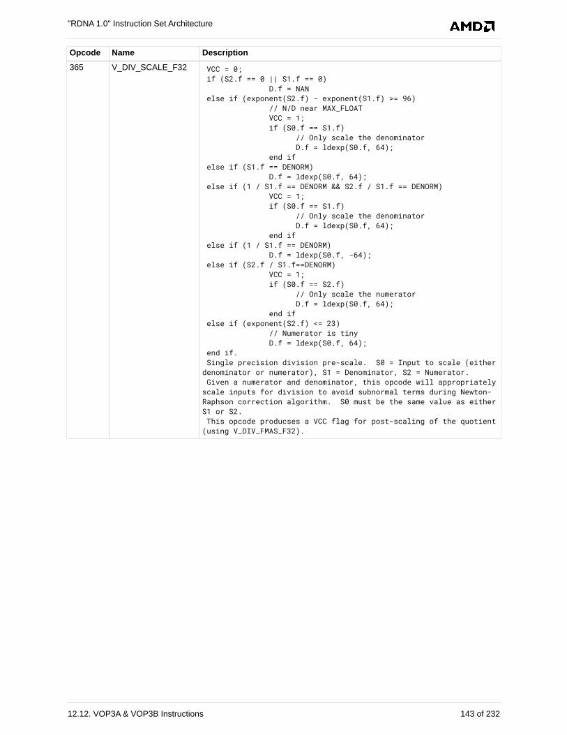
Opcode Name Description
365 V_DIV_SCALE_F32 VCC = 0; if (S2.f == 0 || S1.f == 0) D.f = NAN else if (exponent(S2.f) - exponent(S1.f) >= 96) // N/D near MAX_FLOAT VCC = 1; if (S0.f == S1.f) // Only scale the denominator D.f = ldexp(S0.f, 64); end if else if (S1.f == DENORM) D.f = ldexp(S0.f, 64); else if (1 / S1.f == DENORM && S2.f / S1.f == DENORM) VCC = 1; if (S0.f == S1.f) // Only scale the denominator D.f = ldexp(S0.f, 64); end if else if (1 / S1.f == DENORM) D.f = ldexp(S0.f, -64); else if (S2.f / S1.f==DENORM) VCC = 1; if (S0.f == S2.f) // Only scale the numerator D.f = ldexp(S0.f, 64); end if else if (exponent(S2.f) <= 23) // Numerator is tiny D.f = ldexp(S0.f, 64); end if. Single precision division pre-scale. S0 = Input to scale (eitherdenominator or numerator), S1 = Denominator, S2 = Numerator. Given a numerator and denominator, this opcode will appropriatelyscale inputs for division to avoid subnormal terms during Newton-Raphson correction algorithm. S0 must be the same value as eitherS1 or S2. This opcode producses a VCC flag for post-scaling of the quotient(using V_DIV_FMAS_F32).
"RDNA 1.0" Instruction Set Architecture
12.12. VOP3A & VOP3B Instructions 143 of 232
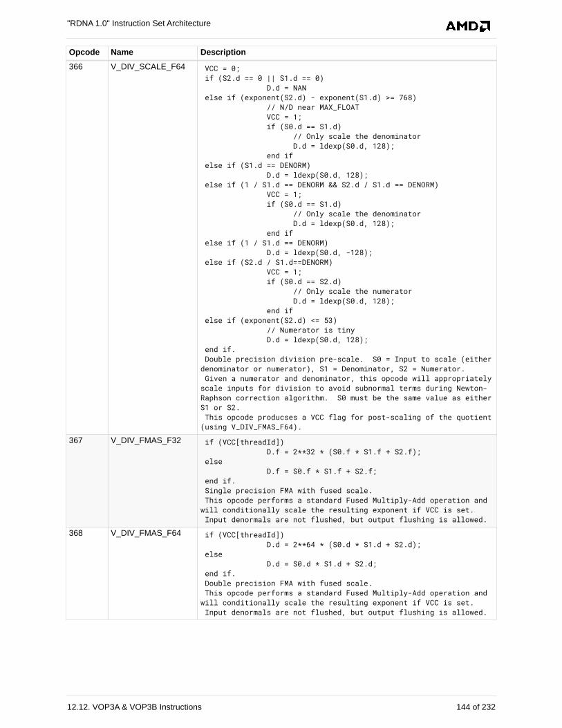
Opcode Name Description
366 V_DIV_SCALE_F64 VCC = 0; if (S2.d == 0 || S1.d == 0) D.d = NAN else if (exponent(S2.d) - exponent(S1.d) >= 768) // N/D near MAX_FLOAT VCC = 1; if (S0.d == S1.d) // Only scale the denominator D.d = ldexp(S0.d, 128); end if else if (S1.d == DENORM) D.d = ldexp(S0.d, 128); else if (1 / S1.d == DENORM && S2.d / S1.d == DENORM) VCC = 1; if (S0.d == S1.d) // Only scale the denominator D.d = ldexp(S0.d, 128); end if else if (1 / S1.d == DENORM) D.d = ldexp(S0.d, -128); else if (S2.d / S1.d==DENORM) VCC = 1; if (S0.d == S2.d) // Only scale the numerator D.d = ldexp(S0.d, 128); end if else if (exponent(S2.d) <= 53) // Numerator is tiny D.d = ldexp(S0.d, 128); end if. Double precision division pre-scale. S0 = Input to scale (eitherdenominator or numerator), S1 = Denominator, S2 = Numerator. Given a numerator and denominator, this opcode will appropriatelyscale inputs for division to avoid subnormal terms during Newton-Raphson correction algorithm. S0 must be the same value as eitherS1 or S2. This opcode producses a VCC flag for post-scaling of the quotient(using V_DIV_FMAS_F64).
367 V_DIV_FMAS_F32 if (VCC[threadId]) D.f = 2**32 * (S0.f * S1.f + S2.f); else D.f = S0.f * S1.f + S2.f; end if. Single precision FMA with fused scale. This opcode performs a standard Fused Multiply-Add operation andwill conditionally scale the resulting exponent if VCC is set. Input denormals are not flushed, but output flushing is allowed.
368 V_DIV_FMAS_F64 if (VCC[threadId]) D.d = 2**64 * (S0.d * S1.d + S2.d); else D.d = S0.d * S1.d + S2.d; end if. Double precision FMA with fused scale. This opcode performs a standard Fused Multiply-Add operation andwill conditionally scale the resulting exponent if VCC is set. Input denormals are not flushed, but output flushing is allowed.
"RDNA 1.0" Instruction Set Architecture
12.12. VOP3A & VOP3B Instructions 144 of 232
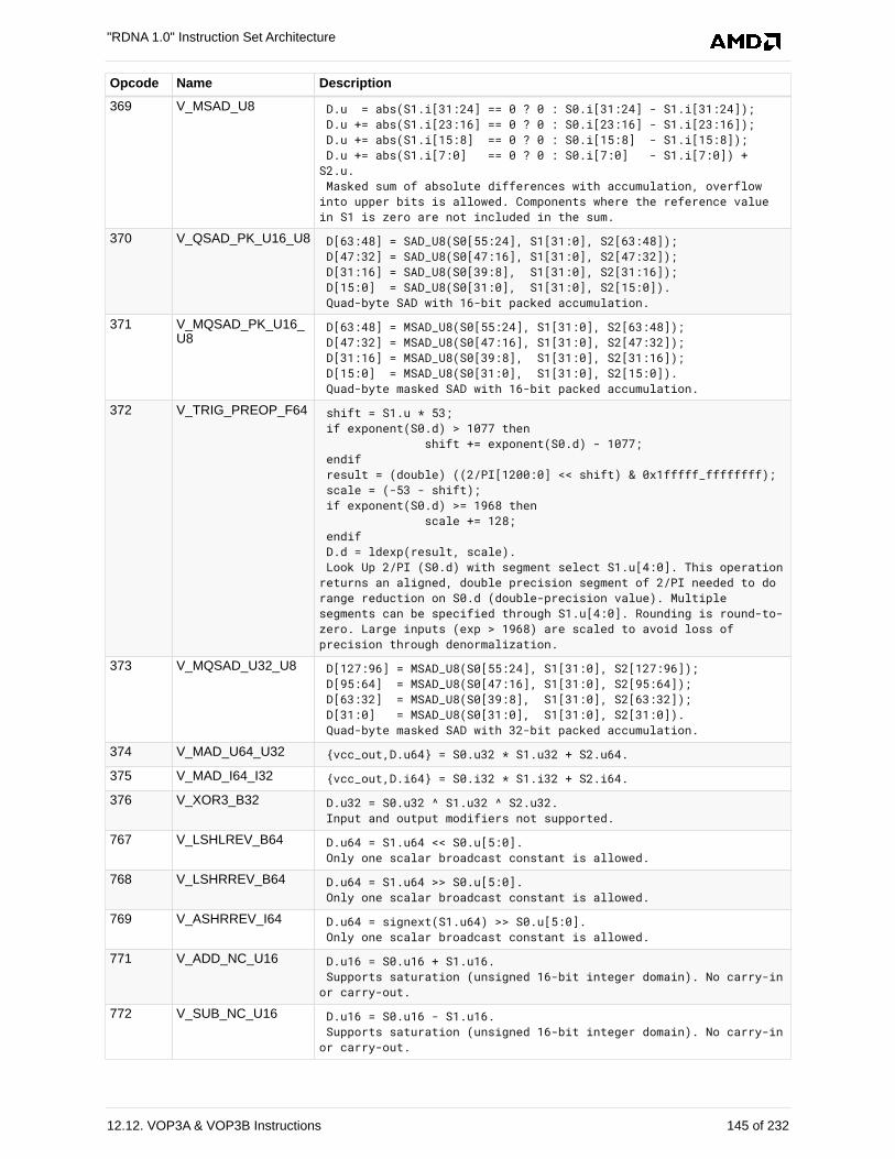
Opcode Name Description
369 V_MSAD_U8 D.u = abs(S1.i[31:24] == 0 ? 0 : S0.i[31:24] - S1.i[31:24]); D.u += abs(S1.i[23:16] == 0 ? 0 : S0.i[23:16] - S1.i[23:16]); D.u += abs(S1.i[15:8] == 0 ? 0 : S0.i[15:8] - S1.i[15:8]); D.u += abs(S1.i[7:0] == 0 ? 0 : S0.i[7:0] - S1.i[7:0]) +S2.u. Masked sum of absolute differences with accumulation, overflowinto upper bits is allowed. Components where the reference valuein S1 is zero are not included in the sum.
370 V_QSAD_PK_U16_U8 D[63:48] = SAD_U8(S0[55:24], S1[31:0], S2[63:48]); D[47:32] = SAD_U8(S0[47:16], S1[31:0], S2[47:32]); D[31:16] = SAD_U8(S0[39:8], S1[31:0], S2[31:16]); D[15:0] = SAD_U8(S0[31:0], S1[31:0], S2[15:0]). Quad-byte SAD with 16-bit packed accumulation.
371 V_MQSAD_PK_U16_U8
D[63:48] = MSAD_U8(S0[55:24], S1[31:0], S2[63:48]); D[47:32] = MSAD_U8(S0[47:16], S1[31:0], S2[47:32]); D[31:16] = MSAD_U8(S0[39:8], S1[31:0], S2[31:16]); D[15:0] = MSAD_U8(S0[31:0], S1[31:0], S2[15:0]). Quad-byte masked SAD with 16-bit packed accumulation.
372 V_TRIG_PREOP_F64 shift = S1.u * 53; if exponent(S0.d) > 1077 then shift += exponent(S0.d) - 1077; endif result = (double) ((2/PI[1200:0] << shift) & 0x1fffff_ffffffff); scale = (-53 - shift); if exponent(S0.d) >= 1968 then scale += 128; endif D.d = ldexp(result, scale). Look Up 2/PI (S0.d) with segment select S1.u[4:0]. This operationreturns an aligned, double precision segment of 2/PI needed to dorange reduction on S0.d (double-precision value). Multiplesegments can be specified through S1.u[4:0]. Rounding is round-to-zero. Large inputs (exp > 1968) are scaled to avoid loss ofprecision through denormalization.
373 V_MQSAD_U32_U8 D[127:96] = MSAD_U8(S0[55:24], S1[31:0], S2[127:96]); D[95:64] = MSAD_U8(S0[47:16], S1[31:0], S2[95:64]); D[63:32] = MSAD_U8(S0[39:8], S1[31:0], S2[63:32]); D[31:0] = MSAD_U8(S0[31:0], S1[31:0], S2[31:0]). Quad-byte masked SAD with 32-bit packed accumulation.
374 V_MAD_U64_U32 {vcc_out,D.u64} = S0.u32 * S1.u32 + S2.u64.
375 V_MAD_I64_I32 {vcc_out,D.i64} = S0.i32 * S1.i32 + S2.i64.
376 V_XOR3_B32 D.u32 = S0.u32 ^ S1.u32 ^ S2.u32. Input and output modifiers not supported.
767 V_LSHLREV_B64 D.u64 = S1.u64 << S0.u[5:0]. Only one scalar broadcast constant is allowed.
768 V_LSHRREV_B64 D.u64 = S1.u64 >> S0.u[5:0]. Only one scalar broadcast constant is allowed.
769 V_ASHRREV_I64 D.u64 = signext(S1.u64) >> S0.u[5:0]. Only one scalar broadcast constant is allowed.
771 V_ADD_NC_U16 D.u16 = S0.u16 + S1.u16. Supports saturation (unsigned 16-bit integer domain). No carry-inor carry-out.
772 V_SUB_NC_U16 D.u16 = S0.u16 - S1.u16. Supports saturation (unsigned 16-bit integer domain). No carry-inor carry-out.
"RDNA 1.0" Instruction Set Architecture
12.12. VOP3A & VOP3B Instructions 145 of 232
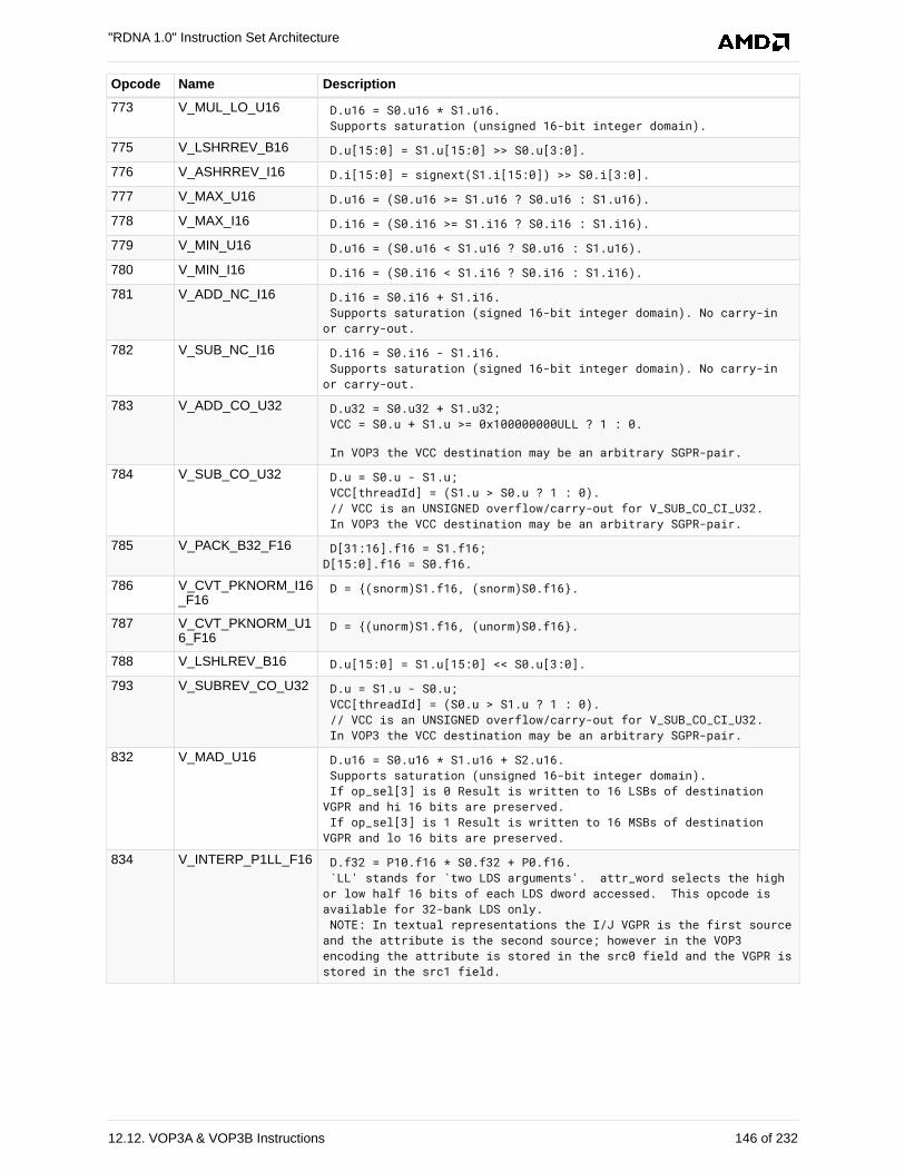
Opcode Name Description
773 V_MUL_LO_U16 D.u16 = S0.u16 * S1.u16. Supports saturation (unsigned 16-bit integer domain).
775 V_LSHRREV_B16 D.u[15:0] = S1.u[15:0] >> S0.u[3:0].
776 V_ASHRREV_I16 D.i[15:0] = signext(S1.i[15:0]) >> S0.i[3:0].
777 V_MAX_U16 D.u16 = (S0.u16 >= S1.u16 ? S0.u16 : S1.u16).
778 V_MAX_I16 D.i16 = (S0.i16 >= S1.i16 ? S0.i16 : S1.i16).
779 V_MIN_U16 D.u16 = (S0.u16 < S1.u16 ? S0.u16 : S1.u16).
780 V_MIN_I16 D.i16 = (S0.i16 < S1.i16 ? S0.i16 : S1.i16).
781 V_ADD_NC_I16 D.i16 = S0.i16 + S1.i16. Supports saturation (signed 16-bit integer domain). No carry-inor carry-out.
782 V_SUB_NC_I16 D.i16 = S0.i16 - S1.i16. Supports saturation (signed 16-bit integer domain). No carry-inor carry-out.
783 V_ADD_CO_U32 D.u32 = S0.u32 + S1.u32; VCC = S0.u + S1.u >= 0x100000000ULL ? 1 : 0.
In VOP3 the VCC destination may be an arbitrary SGPR-pair.
784 V_SUB_CO_U32 D.u = S0.u - S1.u; VCC[threadId] = (S1.u > S0.u ? 1 : 0). // VCC is an UNSIGNED overflow/carry-out for V_SUB_CO_CI_U32. In VOP3 the VCC destination may be an arbitrary SGPR-pair.
785 V_PACK_B32_F16 D[31:16].f16 = S1.f16;D[15:0].f16 = S0.f16.
786 V_CVT_PKNORM_I16_F16
D = {(snorm)S1.f16, (snorm)S0.f16}.
787 V_CVT_PKNORM_U16_F16
D = {(unorm)S1.f16, (unorm)S0.f16}.
788 V_LSHLREV_B16 D.u[15:0] = S1.u[15:0] << S0.u[3:0].
793 V_SUBREV_CO_U32 D.u = S1.u - S0.u; VCC[threadId] = (S0.u > S1.u ? 1 : 0). // VCC is an UNSIGNED overflow/carry-out for V_SUB_CO_CI_U32. In VOP3 the VCC destination may be an arbitrary SGPR-pair.
832 V_MAD_U16 D.u16 = S0.u16 * S1.u16 + S2.u16. Supports saturation (unsigned 16-bit integer domain). If op_sel[3] is 0 Result is written to 16 LSBs of destinationVGPR and hi 16 bits are preserved. If op_sel[3] is 1 Result is written to 16 MSBs of destinationVGPR and lo 16 bits are preserved.
834 V_INTERP_P1LL_F16 D.f32 = P10.f16 * S0.f32 + P0.f16. `LL' stands for `two LDS arguments'. attr_word selects the highor low half 16 bits of each LDS dword accessed. This opcode isavailable for 32-bank LDS only. NOTE: In textual representations the I/J VGPR is the first sourceand the attribute is the second source; however in the VOP3encoding the attribute is stored in the src0 field and the VGPR isstored in the src1 field.
"RDNA 1.0" Instruction Set Architecture
12.12. VOP3A & VOP3B Instructions 146 of 232
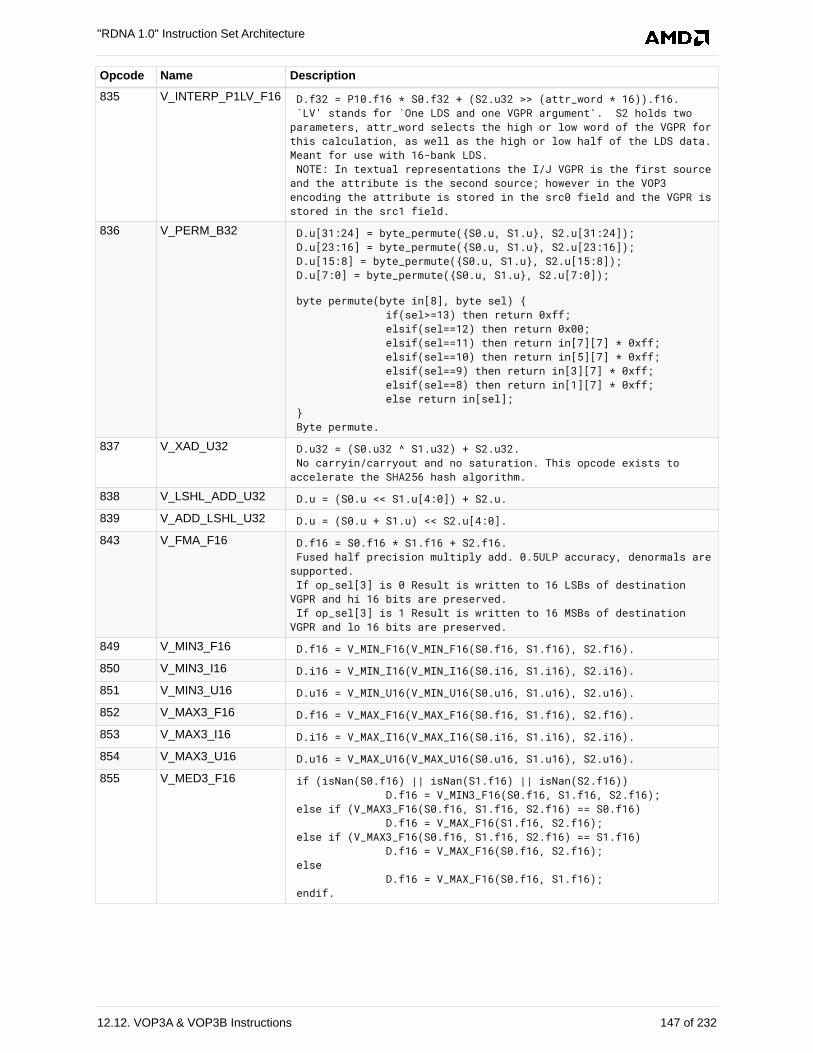
Opcode Name Description
835 V_INTERP_P1LV_F16 D.f32 = P10.f16 * S0.f32 + (S2.u32 >> (attr_word * 16)).f16. `LV' stands for `One LDS and one VGPR argument'. S2 holds twoparameters, attr_word selects the high or low word of the VGPR forthis calculation, as well as the high or low half of the LDS data.Meant for use with 16-bank LDS. NOTE: In textual representations the I/J VGPR is the first sourceand the attribute is the second source; however in the VOP3encoding the attribute is stored in the src0 field and the VGPR isstored in the src1 field.
836 V_PERM_B32 D.u[31:24] = byte_permute({S0.u, S1.u}, S2.u[31:24]); D.u[23:16] = byte_permute({S0.u, S1.u}, S2.u[23:16]); D.u[15:8] = byte_permute({S0.u, S1.u}, S2.u[15:8]); D.u[7:0] = byte_permute({S0.u, S1.u}, S2.u[7:0]);
byte permute(byte in[8], byte sel) { if(sel>=13) then return 0xff; elsif(sel==12) then return 0x00; elsif(sel==11) then return in[7][7] * 0xff; elsif(sel==10) then return in[5][7] * 0xff; elsif(sel==9) then return in[3][7] * 0xff; elsif(sel==8) then return in[1][7] * 0xff; else return in[sel]; } Byte permute.
837 V_XAD_U32 D.u32 = (S0.u32 ^ S1.u32) + S2.u32. No carryin/carryout and no saturation. This opcode exists toaccelerate the SHA256 hash algorithm.
838 V_LSHL_ADD_U32 D.u = (S0.u << S1.u[4:0]) + S2.u.
839 V_ADD_LSHL_U32 D.u = (S0.u + S1.u) << S2.u[4:0].
843 V_FMA_F16 D.f16 = S0.f16 * S1.f16 + S2.f16. Fused half precision multiply add. 0.5ULP accuracy, denormals aresupported. If op_sel[3] is 0 Result is written to 16 LSBs of destinationVGPR and hi 16 bits are preserved. If op_sel[3] is 1 Result is written to 16 MSBs of destinationVGPR and lo 16 bits are preserved.
849 V_MIN3_F16 D.f16 = V_MIN_F16(V_MIN_F16(S0.f16, S1.f16), S2.f16).
850 V_MIN3_I16 D.i16 = V_MIN_I16(V_MIN_I16(S0.i16, S1.i16), S2.i16).
851 V_MIN3_U16 D.u16 = V_MIN_U16(V_MIN_U16(S0.u16, S1.u16), S2.u16).
852 V_MAX3_F16 D.f16 = V_MAX_F16(V_MAX_F16(S0.f16, S1.f16), S2.f16).
853 V_MAX3_I16 D.i16 = V_MAX_I16(V_MAX_I16(S0.i16, S1.i16), S2.i16).
854 V_MAX3_U16 D.u16 = V_MAX_U16(V_MAX_U16(S0.u16, S1.u16), S2.u16).
855 V_MED3_F16 if (isNan(S0.f16) || isNan(S1.f16) || isNan(S2.f16)) D.f16 = V_MIN3_F16(S0.f16, S1.f16, S2.f16); else if (V_MAX3_F16(S0.f16, S1.f16, S2.f16) == S0.f16) D.f16 = V_MAX_F16(S1.f16, S2.f16); else if (V_MAX3_F16(S0.f16, S1.f16, S2.f16) == S1.f16) D.f16 = V_MAX_F16(S0.f16, S2.f16); else D.f16 = V_MAX_F16(S0.f16, S1.f16); endif.
"RDNA 1.0" Instruction Set Architecture
12.12. VOP3A & VOP3B Instructions 147 of 232
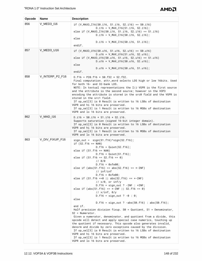
Opcode Name Description
856 V_MED3_I16 if (V_MAX3_I16(S0.i16, S1.i16, S2.i16) == S0.i16) D.i16 = V_MAX_I16(S1.i16, S2.i16); else if (V_MAX3_I16(S0.i16, S1.i16, S2.i16) == S1.i16) D.i16 = V_MAX_I16(S0.i16, S2.i16); else D.i16 = V_MAX_I16(S0.i16, S1.i16); endif.
857 V_MED3_U16 if (V_MAX3_U16(S0.u16, S1.u16, S2.u16) == S0.u16) D.u16 = V_MAX_U16(S1.u16, S2.u16); else if (V_MAX3_U16(S0.u16, S1.u16, S2.u16) == S1.u16) D.u16 = V_MAX_U16(S0.u16, S2.u16); else D.u16 = V_MAX_U16(S0.u16, S1.u16); endif.
858 V_INTERP_P2_F16 D.f16 = P20.f16 * S0.f32 + S2.f32. Final computation. attr_word selects LDS high or low 16bits. Usedfor both 16- and 32-bank LDS. NOTE: In textual representations the I/J VGPR is the first sourceand the attribute is the second source; however in the VOP3encoding the attribute is stored in the src0 field and the VGPR isstored in the src1 field. If op_sel[3] is 0 Result is written to 16 LSBs of destinationVGPR and hi 16 bits are preserved. If op_sel[3] is 1 Result is written to 16 MSBs of destinationVGPR and lo 16 bits are preserved.
862 V_MAD_I16 D.i16 = S0.i16 * S1.i16 + S2.i16. Supports saturation (signed 16-bit integer domain). If op_sel[3] is 0 Result is written to 16 LSBs of destinationVGPR and hi 16 bits are preserved. If op_sel[3] is 1 Result is written to 16 MSBs of destinationVGPR and lo 16 bits are preserved.
863 V_DIV_FIXUP_F16 sign_out = sign(S1.f16)^sign(S2.f16); if (S2.f16 == NAN) D.f16 = Quiet(S2.f16); else if (S1.f16 == NAN) D.f16 = Quiet(S1.f16); else if (S1.f16 == S2.f16 == 0) // 0/0 D.f16 = 0xfe00; else if (abs(S1.f16) == abs(S2.f16) == +-INF) // inf/inf D.f16 = 0xfe00; else if (S1.f16 ==0 || abs(S2.f16) == +-INF) // x/0, or inf/y D.f16 = sign_out ? -INF : +INF; else if (abs(S1.f16) == +-INF || S2.f16 == 0) // x/inf, 0/y D.f16 = sign_out ? -0 : 0; else D.f16 = sign_out ? -abs(S0.f16) : abs(S0.f16); end if. Half precision division fixup. S0 = Quotient, S1 = Denominator,S2 = Numerator. Given a numerator, denominator, and quotient from a divide, thisopcode will detect and apply special case numerics, touching upthe quotient if necessary. This opcode also generates invalid,denorm and divide by zero exceptions caused by the division. If op_sel[3] is 0 Result is written to 16 LSBs of destinationVGPR and hi 16 bits are preserved. If op_sel[3] is 1 Result is written to 16 MSBs of destinationVGPR and lo 16 bits are preserved.
"RDNA 1.0" Instruction Set Architecture
12.12. VOP3A & VOP3B Instructions 148 of 232
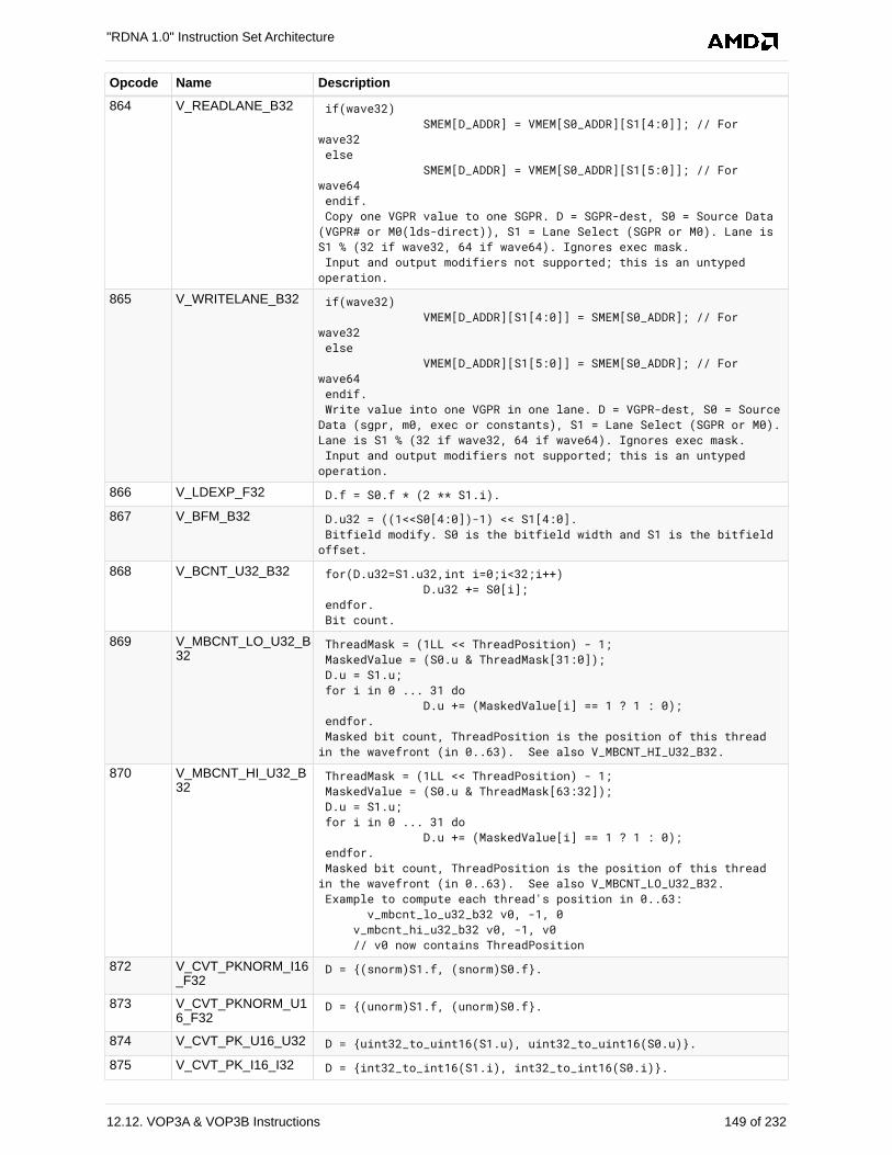
Opcode Name Description
864 V_READLANE_B32 if(wave32) SMEM[D_ADDR] = VMEM[S0_ADDR][S1[4:0]]; // Forwave32 else SMEM[D_ADDR] = VMEM[S0_ADDR][S1[5:0]]; // Forwave64 endif. Copy one VGPR value to one SGPR. D = SGPR-dest, S0 = Source Data(VGPR# or M0(lds-direct)), S1 = Lane Select (SGPR or M0). Lane isS1 % (32 if wave32, 64 if wave64). Ignores exec mask. Input and output modifiers not supported; this is an untypedoperation.
865 V_WRITELANE_B32 if(wave32) VMEM[D_ADDR][S1[4:0]] = SMEM[S0_ADDR]; // Forwave32 else VMEM[D_ADDR][S1[5:0]] = SMEM[S0_ADDR]; // Forwave64 endif. Write value into one VGPR in one lane. D = VGPR-dest, S0 = SourceData (sgpr, m0, exec or constants), S1 = Lane Select (SGPR or M0).Lane is S1 % (32 if wave32, 64 if wave64). Ignores exec mask. Input and output modifiers not supported; this is an untypedoperation.
866 V_LDEXP_F32 D.f = S0.f * (2 ** S1.i).
867 V_BFM_B32 D.u32 = ((1<<S0[4:0])-1) << S1[4:0]. Bitfield modify. S0 is the bitfield width and S1 is the bitfieldoffset.
868 V_BCNT_U32_B32 for(D.u32=S1.u32,int i=0;i<32;i++) D.u32 += S0[i]; endfor. Bit count.
869 V_MBCNT_LO_U32_B32
ThreadMask = (1LL << ThreadPosition) - 1; MaskedValue = (S0.u & ThreadMask[31:0]); D.u = S1.u; for i in 0 ... 31 do D.u += (MaskedValue[i] == 1 ? 1 : 0); endfor. Masked bit count, ThreadPosition is the position of this threadin the wavefront (in 0..63). See also V_MBCNT_HI_U32_B32.
870 V_MBCNT_HI_U32_B32
ThreadMask = (1LL << ThreadPosition) - 1; MaskedValue = (S0.u & ThreadMask[63:32]); D.u = S1.u; for i in 0 ... 31 do D.u += (MaskedValue[i] == 1 ? 1 : 0); endfor. Masked bit count, ThreadPosition is the position of this threadin the wavefront (in 0..63). See also V_MBCNT_LO_U32_B32. Example to compute each thread's position in 0..63: v_mbcnt_lo_u32_b32 v0, -1, 0 v_mbcnt_hi_u32_b32 v0, -1, v0 // v0 now contains ThreadPosition
872 V_CVT_PKNORM_I16_F32
D = {(snorm)S1.f, (snorm)S0.f}.
873 V_CVT_PKNORM_U16_F32
D = {(unorm)S1.f, (unorm)S0.f}.
874 V_CVT_PK_U16_U32 D = {uint32_to_uint16(S1.u), uint32_to_uint16(S0.u)}.
875 V_CVT_PK_I16_I32 D = {int32_to_int16(S1.i), int32_to_int16(S0.i)}.
"RDNA 1.0" Instruction Set Architecture
12.12. VOP3A & VOP3B Instructions 149 of 232
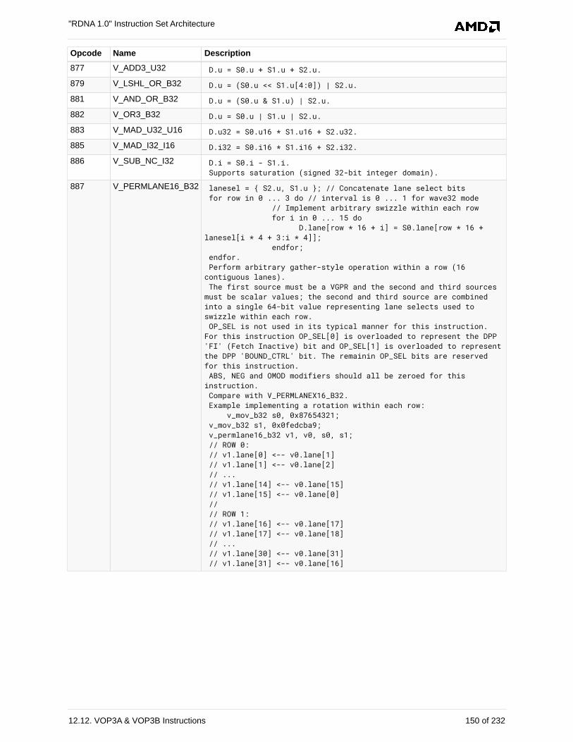
Opcode Name Description
877 V_ADD3_U32 D.u = S0.u + S1.u + S2.u.
879 V_LSHL_OR_B32 D.u = (S0.u << S1.u[4:0]) | S2.u.
881 V_AND_OR_B32 D.u = (S0.u & S1.u) | S2.u.
882 V_OR3_B32 D.u = S0.u | S1.u | S2.u.
883 V_MAD_U32_U16 D.u32 = S0.u16 * S1.u16 + S2.u32.
885 V_MAD_I32_I16 D.i32 = S0.i16 * S1.i16 + S2.i32.
886 V_SUB_NC_I32 D.i = S0.i - S1.i. Supports saturation (signed 32-bit integer domain).
887 V_PERMLANE16_B32 lanesel = { S2.u, S1.u }; // Concatenate lane select bits for row in 0 ... 3 do // interval is 0 ... 1 for wave32 mode // Implement arbitrary swizzle within each row for i in 0 ... 15 do D.lane[row * 16 + i] = S0.lane[row * 16 +lanesel[i * 4 + 3:i * 4]]; endfor; endfor. Perform arbitrary gather-style operation within a row (16contiguous lanes). The first source must be a VGPR and the second and third sourcesmust be scalar values; the second and third source are combinedinto a single 64-bit value representing lane selects used toswizzle within each row. OP_SEL is not used in its typical manner for this instruction.For this instruction OP_SEL[0] is overloaded to represent the DPP'FI' (Fetch Inactive) bit and OP_SEL[1] is overloaded to representthe DPP 'BOUND_CTRL' bit. The remainin OP_SEL bits are reservedfor this instruction. ABS, NEG and OMOD modifiers should all be zeroed for thisinstruction. Compare with V_PERMLANEX16_B32. Example implementing a rotation within each row: v_mov_b32 s0, 0x87654321; v_mov_b32 s1, 0x0fedcba9; v_permlane16_b32 v1, v0, s0, s1; // ROW 0: // v1.lane[0] <-- v0.lane[1] // v1.lane[1] <-- v0.lane[2] // ... // v1.lane[14] <-- v0.lane[15] // v1.lane[15] <-- v0.lane[0] // // ROW 1: // v1.lane[16] <-- v0.lane[17] // v1.lane[17] <-- v0.lane[18] // ... // v1.lane[30] <-- v0.lane[31] // v1.lane[31] <-- v0.lane[16]
"RDNA 1.0" Instruction Set Architecture
12.12. VOP3A & VOP3B Instructions 150 of 232
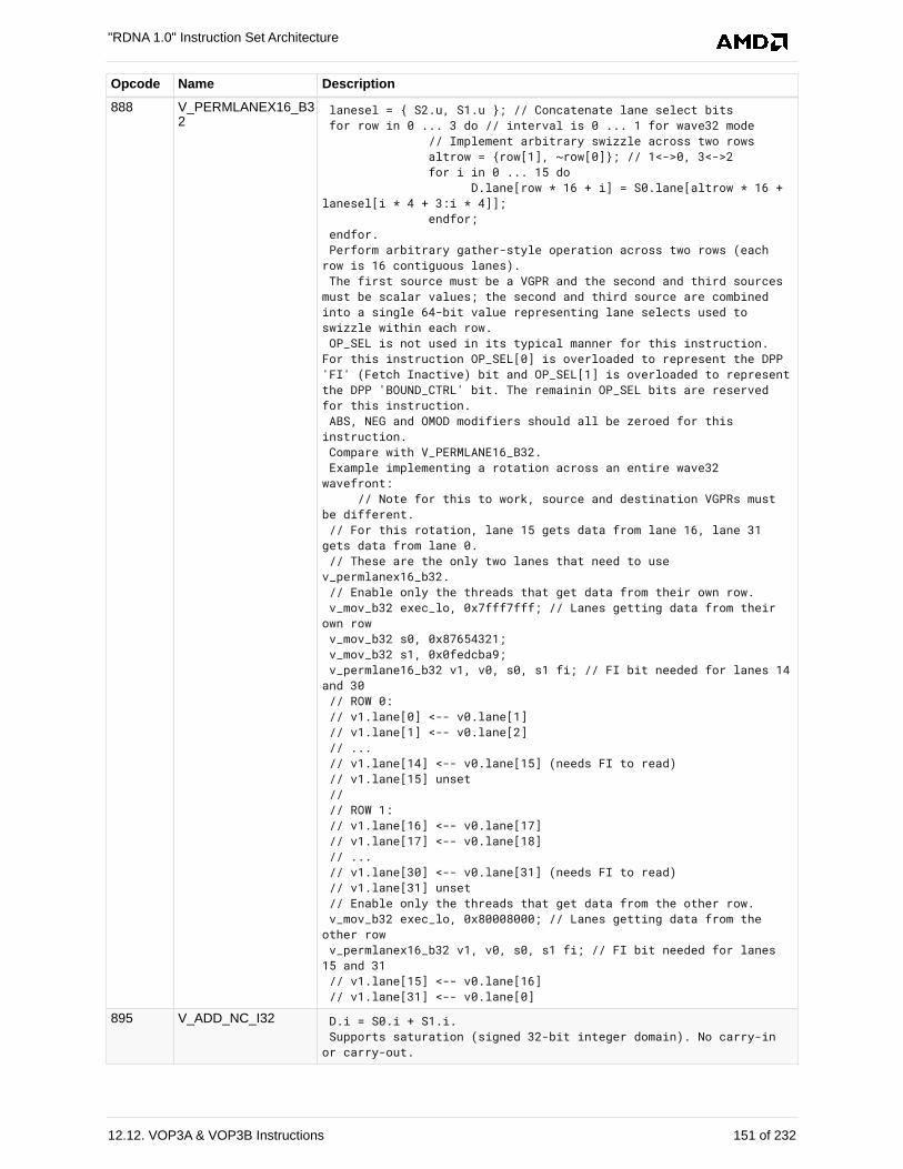
Opcode Name Description
888 V_PERMLANEX16_B32
lanesel = { S2.u, S1.u }; // Concatenate lane select bits for row in 0 ... 3 do // interval is 0 ... 1 for wave32 mode // Implement arbitrary swizzle across two rows altrow = {row[1], ~row[0]}; // 1<->0, 3<->2 for i in 0 ... 15 do D.lane[row * 16 + i] = S0.lane[altrow * 16 +lanesel[i * 4 + 3:i * 4]]; endfor; endfor. Perform arbitrary gather-style operation across two rows (eachrow is 16 contiguous lanes). The first source must be a VGPR and the second and third sourcesmust be scalar values; the second and third source are combinedinto a single 64-bit value representing lane selects used toswizzle within each row. OP_SEL is not used in its typical manner for this instruction.For this instruction OP_SEL[0] is overloaded to represent the DPP'FI' (Fetch Inactive) bit and OP_SEL[1] is overloaded to representthe DPP 'BOUND_CTRL' bit. The remainin OP_SEL bits are reservedfor this instruction. ABS, NEG and OMOD modifiers should all be zeroed for thisinstruction. Compare with V_PERMLANE16_B32. Example implementing a rotation across an entire wave32wavefront: // Note for this to work, source and destination VGPRs mustbe different. // For this rotation, lane 15 gets data from lane 16, lane 31gets data from lane 0. // These are the only two lanes that need to usev_permlanex16_b32. // Enable only the threads that get data from their own row. v_mov_b32 exec_lo, 0x7fff7fff; // Lanes getting data from theirown row v_mov_b32 s0, 0x87654321; v_mov_b32 s1, 0x0fedcba9; v_permlane16_b32 v1, v0, s0, s1 fi; // FI bit needed for lanes 14and 30 // ROW 0: // v1.lane[0] <-- v0.lane[1] // v1.lane[1] <-- v0.lane[2] // ... // v1.lane[14] <-- v0.lane[15] (needs FI to read) // v1.lane[15] unset // // ROW 1: // v1.lane[16] <-- v0.lane[17] // v1.lane[17] <-- v0.lane[18] // ... // v1.lane[30] <-- v0.lane[31] (needs FI to read) // v1.lane[31] unset // Enable only the threads that get data from the other row. v_mov_b32 exec_lo, 0x80008000; // Lanes getting data from theother row v_permlanex16_b32 v1, v0, s0, s1 fi; // FI bit needed for lanes15 and 31 // v1.lane[15] <-- v0.lane[16] // v1.lane[31] <-- v0.lane[0]
895 V_ADD_NC_I32 D.i = S0.i + S1.i. Supports saturation (signed 32-bit integer domain). No carry-inor carry-out.
"RDNA 1.0" Instruction Set Architecture
12.12. VOP3A & VOP3B Instructions 151 of 232
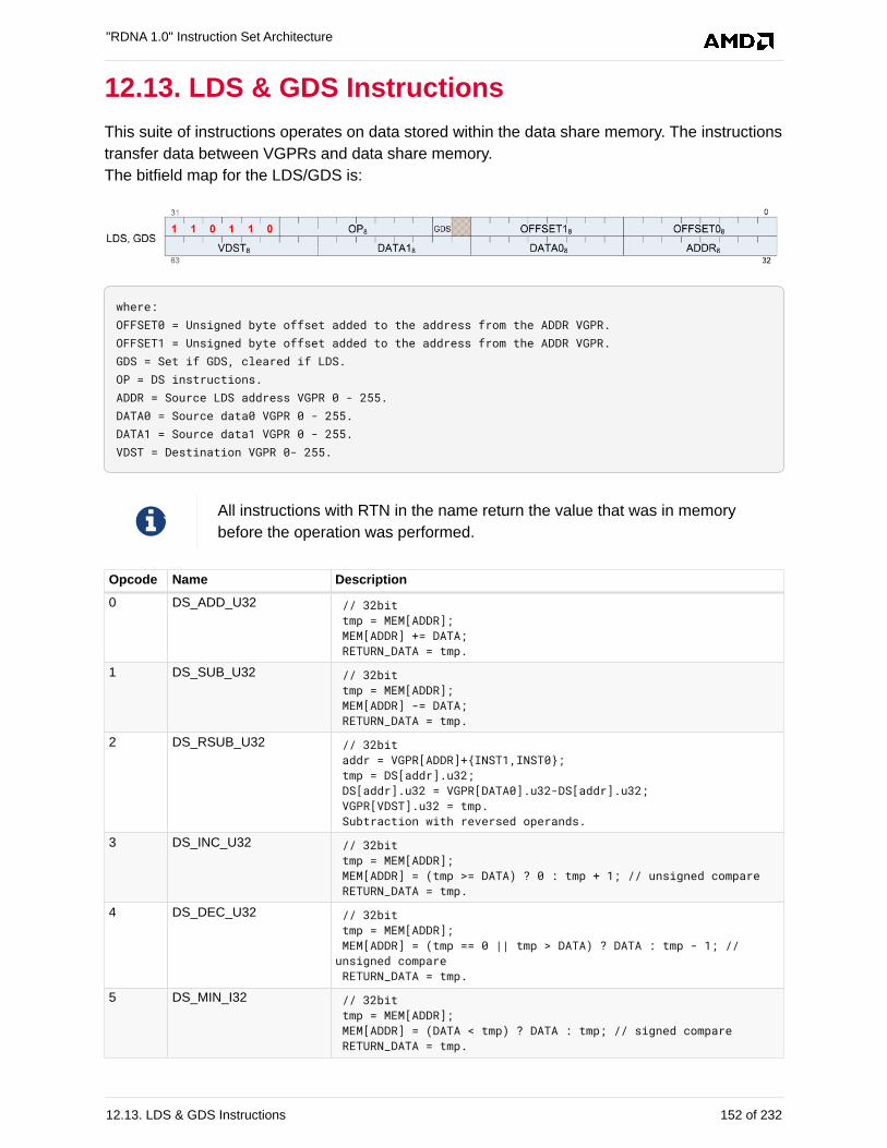
12.13. LDS & GDS Instructions
This suite of instructions operates on data stored within the data share memory. The instructions
transfer data between VGPRs and data share memory.
The bitfield map for the LDS/GDS is:
where:OFFSET0 = Unsigned byte offset added to the address from the ADDR VGPR.OFFSET1 = Unsigned byte offset added to the address from the ADDR VGPR.GDS = Set if GDS, cleared if LDS.OP = DS instructions.ADDR = Source LDS address VGPR 0 - 255.DATA0 = Source data0 VGPR 0 - 255.DATA1 = Source data1 VGPR 0 - 255.VDST = Destination VGPR 0- 255.
All instructions with RTN in the name return the value that was in memory
before the operation was performed.
Opcode Name Description
0 DS_ADD_U32 // 32bit tmp = MEM[ADDR]; MEM[ADDR] += DATA; RETURN_DATA = tmp.
1 DS_SUB_U32 // 32bit tmp = MEM[ADDR]; MEM[ADDR] -= DATA; RETURN_DATA = tmp.
2 DS_RSUB_U32 // 32bit addr = VGPR[ADDR]+{INST1,INST0}; tmp = DS[addr].u32; DS[addr].u32 = VGPR[DATA0].u32-DS[addr].u32; VGPR[VDST].u32 = tmp. Subtraction with reversed operands.
3 DS_INC_U32 // 32bit tmp = MEM[ADDR]; MEM[ADDR] = (tmp >= DATA) ? 0 : tmp + 1; // unsigned compare RETURN_DATA = tmp.
4 DS_DEC_U32 // 32bit tmp = MEM[ADDR]; MEM[ADDR] = (tmp == 0 || tmp > DATA) ? DATA : tmp - 1; //unsigned compare RETURN_DATA = tmp.
5 DS_MIN_I32 // 32bit tmp = MEM[ADDR]; MEM[ADDR] = (DATA < tmp) ? DATA : tmp; // signed compare RETURN_DATA = tmp.
"RDNA 1.0" Instruction Set Architecture
12.13. LDS & GDS Instructions 152 of 232
Opcode Name Description
6 DS_MAX_I32 // 32bit tmp = MEM[ADDR]; MEM[ADDR] = (DATA > tmp) ? DATA : tmp; // signed compare RETURN_DATA = tmp.
7 DS_MIN_U32 // 32bit tmp = MEM[ADDR]; MEM[ADDR] = (DATA < tmp) ? DATA : tmp; // unsigned compare RETURN_DATA = tmp.
8 DS_MAX_U32 // 32bit tmp = MEM[ADDR]; MEM[ADDR] = (DATA > tmp) ? DATA : tmp; // unsigned compare RETURN_DATA = tmp.
9 DS_AND_B32 // 32bit tmp = MEM[ADDR]; MEM[ADDR] &= DATA; RETURN_DATA = tmp.
10 DS_OR_B32 // 32bit tmp = MEM[ADDR]; MEM[ADDR] |= DATA; RETURN_DATA = tmp.
11 DS_XOR_B32 // 32bit tmp = MEM[ADDR]; MEM[ADDR] ^= DATA; RETURN_DATA = tmp.
12 DS_MSKOR_B32 // 32bit tmp = MEM[ADDR]; MEM[ADDR] = (MEM[ADDR] & ~DATA) | DATA2; RETURN_DATA = tmp. Masked dword OR, D0 contains the mask and D1 contains the newvalue.
13 DS_WRITE_B32 // 32bit MEM[ADDR] = DATA. Write dword.
14 DS_WRITE2_B32 // 32bit MEM[ADDR + OFFSET0 * 4] = DATA; MEM[ADDR + OFFSET1 * 4] = DATA2. Write 2 dwords.
15 DS_WRITE2ST64_B32 // 32bit MEM[ADDR + OFFSET0 * 4 * 64] = DATA; MEM[ADDR + OFFSET1 * 4 * 64] = DATA2. Write 2 dwords.
16 DS_CMPST_B32 // 32bit tmp = MEM[ADDR]; src = DATA2; cmp = DATA; MEM[ADDR] = (tmp == cmp) ? src : tmp; RETURN_DATA[0] = tmp. Compare and store. Caution, the order of src and cmp are the*opposite* of the BUFFER_ATOMIC_CMPSWAP opcode.
"RDNA 1.0" Instruction Set Architecture
12.13. LDS & GDS Instructions 153 of 232
Opcode Name Description
17 DS_CMPST_F32 // 32bit tmp = MEM[ADDR]; src = DATA2; cmp = DATA; MEM[ADDR] = (tmp == cmp) ? src : tmp; RETURN_DATA[0] = tmp. Floating point compare and store that handles NaN/INF/denormalvalues. Caution, the order of src and cmp are the *opposite*of the BUFFER_ATOMIC_FCMPSWAP opcode.
18 DS_MIN_F32 // 32bit tmp = MEM[ADDR]; src = DATA; cmp = DATA2; MEM[ADDR] = (cmp < tmp) ? src : tmp. Floating point minimum that handles NaN/INF/denormal values.Note that this opcode is slightly more general-purpose thanBUFFER_ATOMIC_FMIN.
19 DS_MAX_F32 // 32bit tmp = MEM[ADDR]; src = DATA; cmp = DATA2; MEM[ADDR] = (tmp > cmp) ? src : tmp. Floating point maximum that handles NaN/INF/denormal values.Note that this opcode is slightly more general-purpose thanBUFFER_ATOMIC_FMAX.
20 DS_NOP Do nothing.
21 DS_ADD_F32 float tmp = MEM[ADDR].f32; MEM[ADDR].f32 += DATA0.f32; VDST.f32 = tmp; Floating point add that handles NaN/INF/denormal values.
24 DS_GWS_SEMA_RELEASE_ALL
GDS Only: The GWS resource (rid) indicated will process thisopcode by updating the counter and labeling the specifiedresource as a semaphore. // Determine the GWS resource to work on rid[5:0] = SH_SX_EXPCMD.gds_base[5:0] + offset0[5:0]; // Incr the state counter of the resource state.counter[rid] = state.wave_in_queue; state.type = SEMAPHORE; return rd_done; //release calling wave This action will release ALL queued waves; it Will have noeffect if no waves are present.
25 DS_GWS_INIT GDS Only: Initialize a barrier or semaphore resource. // Determine the GWS resource to work on rid[5:0] = SH_SX_EXPCMD.gds_base[5:0] + offset0[5:0]; // Get the value to use in init index = find_first_valid(vector mask) value = DATA[thread: index] // Set the state of the resource state.counter[rid] = lsb(value); //limit #waves state.flag[rid] = 0; return rd_done; //release calling wave
"RDNA 1.0" Instruction Set Architecture
12.13. LDS & GDS Instructions 154 of 232
Opcode Name Description
26 DS_GWS_SEMA_V GDS Only: The GWS resource indicated will process this opcodeby updating the counter and labeling the resource as asemaphore. //Determine the GWS resource to work on rid[5:0] = SH_SX_EXPCMD.gds_base[5:0] + offset0[5:0]; //Incr the state counter of the resource state.counter[rid] += 1; state.type = SEMAPHORE; return rd_done; //release calling wave This action will release one waved if any are queued in thisresource.
27 DS_GWS_SEMA_BR GDS Only: The GWS resource indicated will process this opcodeby updating the counter by the bulk release delivered count andlabeling the resource as a semaphore. //Determine the GWS resource to work on rid[5:0] = SH_SX_EXPCMD.gds_base[5:0] + offset0[5:0]; index = find first valid (vector mask) count = DATA[thread: index]; //Add count to the resource state counter state.counter[rid] += count; state.type = SEMAPHORE; return rd_done; //release calling wave This action will release count number of waves, immediately ifqueued, or as they arrive from the noted resource.
28 DS_GWS_SEMA_P GDS Only: The GWS resource indicated will process this opcodeby queueing it until counter enables a release and thendecrementing the counter of the resource as a semaphore. //Determine the GWS resource to work on rid[5:0] = SH_SX_EXPCMD.gds_base[5:0] + offset0[5:0]; state.type = SEMAPHORE; ENQUEUE until(state[rid].counter > 0) state[rid].counter -= 1; return rd_done;
29 DS_GWS_BARRIER GDS Only: The GWS resource indicated will process this opcodeby queueing it until barrier is satisfied. The number of wavesneeded is passed in as DATA of first valid thread. //Determine the GWS resource to work on rid[5:0] = SH_SX_EXPCMD.gds_base[5:0] + OFFSET0[5:0]; index = find first valid (vector mask); value = DATA[thread: index]; // Input Decision Machine state.type[rid] = BARRIER; if(state[rid].counter <= 0) then thread[rid].flag = state[rid].flag; ENQUEUE; state[rid].flag = !state.flag; state[rid].counter = value; return rd_done; else state[rid].counter -= 1; thread.flag = state[rid].flag; ENQUEUE; endif. Since the waves deliver the count for the next barrier, thisfunction can have a different size barrier for each occurrence. // Release Machine if(state.type == BARRIER) then if(state.flag != thread.flag) then return rd_done; endif; endif.
"RDNA 1.0" Instruction Set Architecture
12.13. LDS & GDS Instructions 155 of 232
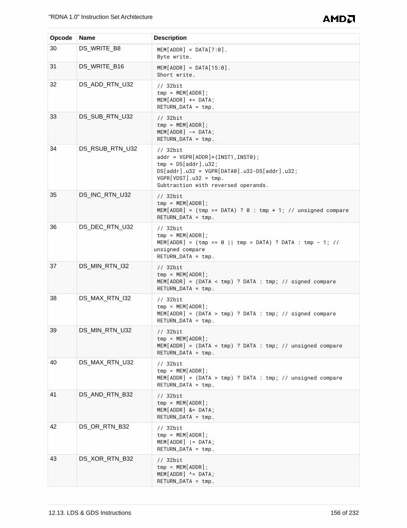
Opcode Name Description
30 DS_WRITE_B8 MEM[ADDR] = DATA[7:0]. Byte write.
31 DS_WRITE_B16 MEM[ADDR] = DATA[15:0]. Short write.
32 DS_ADD_RTN_U32 // 32bit tmp = MEM[ADDR]; MEM[ADDR] += DATA; RETURN_DATA = tmp.
33 DS_SUB_RTN_U32 // 32bit tmp = MEM[ADDR]; MEM[ADDR] -= DATA; RETURN_DATA = tmp.
34 DS_RSUB_RTN_U32 // 32bit addr = VGPR[ADDR]+{INST1,INST0}; tmp = DS[addr].u32; DS[addr].u32 = VGPR[DATA0].u32-DS[addr].u32; VGPR[VDST].u32 = tmp. Subtraction with reversed operands.
35 DS_INC_RTN_U32 // 32bit tmp = MEM[ADDR]; MEM[ADDR] = (tmp >= DATA) ? 0 : tmp + 1; // unsigned compare RETURN_DATA = tmp.
36 DS_DEC_RTN_U32 // 32bit tmp = MEM[ADDR]; MEM[ADDR] = (tmp == 0 || tmp > DATA) ? DATA : tmp - 1; //unsigned compare RETURN_DATA = tmp.
37 DS_MIN_RTN_I32 // 32bit tmp = MEM[ADDR]; MEM[ADDR] = (DATA < tmp) ? DATA : tmp; // signed compare RETURN_DATA = tmp.
38 DS_MAX_RTN_I32 // 32bit tmp = MEM[ADDR]; MEM[ADDR] = (DATA > tmp) ? DATA : tmp; // signed compare RETURN_DATA = tmp.
39 DS_MIN_RTN_U32 // 32bit tmp = MEM[ADDR]; MEM[ADDR] = (DATA < tmp) ? DATA : tmp; // unsigned compare RETURN_DATA = tmp.
40 DS_MAX_RTN_U32 // 32bit tmp = MEM[ADDR]; MEM[ADDR] = (DATA > tmp) ? DATA : tmp; // unsigned compare RETURN_DATA = tmp.
41 DS_AND_RTN_B32 // 32bit tmp = MEM[ADDR]; MEM[ADDR] &= DATA; RETURN_DATA = tmp.
42 DS_OR_RTN_B32 // 32bit tmp = MEM[ADDR]; MEM[ADDR] |= DATA; RETURN_DATA = tmp.
43 DS_XOR_RTN_B32 // 32bit tmp = MEM[ADDR]; MEM[ADDR] ^= DATA; RETURN_DATA = tmp.
"RDNA 1.0" Instruction Set Architecture
12.13. LDS & GDS Instructions 156 of 232
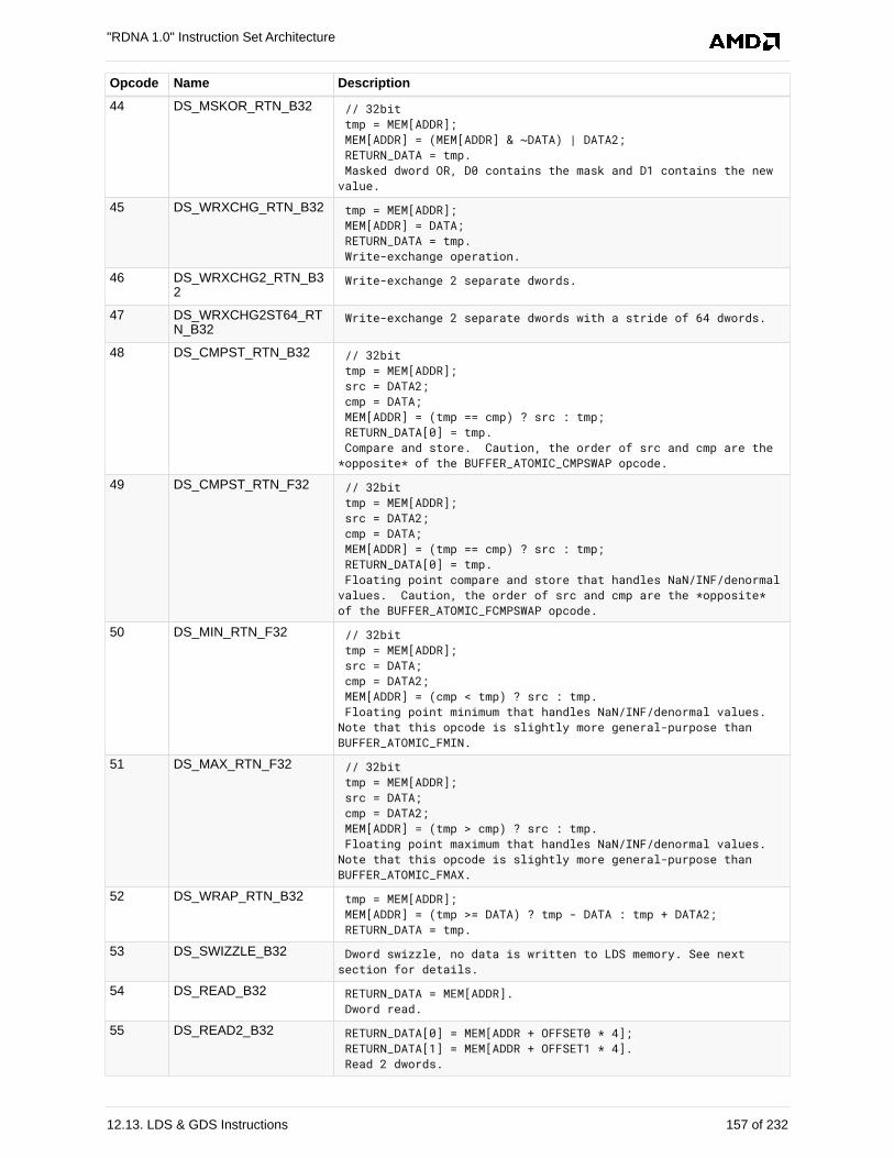
Opcode Name Description
44 DS_MSKOR_RTN_B32 // 32bit tmp = MEM[ADDR]; MEM[ADDR] = (MEM[ADDR] & ~DATA) | DATA2; RETURN_DATA = tmp. Masked dword OR, D0 contains the mask and D1 contains the newvalue.
45 DS_WRXCHG_RTN_B32 tmp = MEM[ADDR]; MEM[ADDR] = DATA; RETURN_DATA = tmp. Write-exchange operation.
46 DS_WRXCHG2_RTN_B32
Write-exchange 2 separate dwords.
47 DS_WRXCHG2ST64_RTN_B32
Write-exchange 2 separate dwords with a stride of 64 dwords.
48 DS_CMPST_RTN_B32 // 32bit tmp = MEM[ADDR]; src = DATA2; cmp = DATA; MEM[ADDR] = (tmp == cmp) ? src : tmp; RETURN_DATA[0] = tmp. Compare and store. Caution, the order of src and cmp are the*opposite* of the BUFFER_ATOMIC_CMPSWAP opcode.
49 DS_CMPST_RTN_F32 // 32bit tmp = MEM[ADDR]; src = DATA2; cmp = DATA; MEM[ADDR] = (tmp == cmp) ? src : tmp; RETURN_DATA[0] = tmp. Floating point compare and store that handles NaN/INF/denormalvalues. Caution, the order of src and cmp are the *opposite*of the BUFFER_ATOMIC_FCMPSWAP opcode.
50 DS_MIN_RTN_F32 // 32bit tmp = MEM[ADDR]; src = DATA; cmp = DATA2; MEM[ADDR] = (cmp < tmp) ? src : tmp. Floating point minimum that handles NaN/INF/denormal values.Note that this opcode is slightly more general-purpose thanBUFFER_ATOMIC_FMIN.
51 DS_MAX_RTN_F32 // 32bit tmp = MEM[ADDR]; src = DATA; cmp = DATA2; MEM[ADDR] = (tmp > cmp) ? src : tmp. Floating point maximum that handles NaN/INF/denormal values.Note that this opcode is slightly more general-purpose thanBUFFER_ATOMIC_FMAX.
52 DS_WRAP_RTN_B32 tmp = MEM[ADDR]; MEM[ADDR] = (tmp >= DATA) ? tmp - DATA : tmp + DATA2; RETURN_DATA = tmp.
53 DS_SWIZZLE_B32 Dword swizzle, no data is written to LDS memory. See nextsection for details.
54 DS_READ_B32 RETURN_DATA = MEM[ADDR]. Dword read.
55 DS_READ2_B32 RETURN_DATA[0] = MEM[ADDR + OFFSET0 * 4]; RETURN_DATA[1] = MEM[ADDR + OFFSET1 * 4]. Read 2 dwords.
"RDNA 1.0" Instruction Set Architecture
12.13. LDS & GDS Instructions 157 of 232
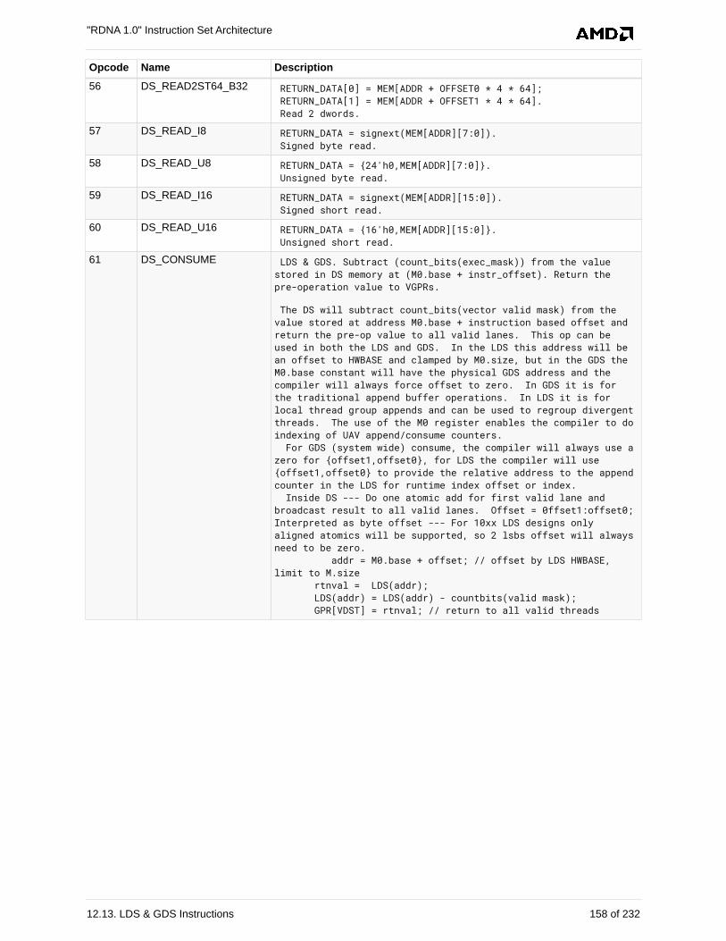
Opcode Name Description
56 DS_READ2ST64_B32 RETURN_DATA[0] = MEM[ADDR + OFFSET0 * 4 * 64]; RETURN_DATA[1] = MEM[ADDR + OFFSET1 * 4 * 64]. Read 2 dwords.
57 DS_READ_I8 RETURN_DATA = signext(MEM[ADDR][7:0]). Signed byte read.
58 DS_READ_U8 RETURN_DATA = {24'h0,MEM[ADDR][7:0]}. Unsigned byte read.
59 DS_READ_I16 RETURN_DATA = signext(MEM[ADDR][15:0]). Signed short read.
60 DS_READ_U16 RETURN_DATA = {16'h0,MEM[ADDR][15:0]}. Unsigned short read.
61 DS_CONSUME LDS & GDS. Subtract (count_bits(exec_mask)) from the valuestored in DS memory at (M0.base + instr_offset). Return thepre-operation value to VGPRs.
The DS will subtract count_bits(vector valid mask) from thevalue stored at address M0.base + instruction based offset andreturn the pre-op value to all valid lanes. This op can beused in both the LDS and GDS. In the LDS this address will bean offset to HWBASE and clamped by M0.size, but in the GDS theM0.base constant will have the physical GDS address and thecompiler will always force offset to zero. In GDS it is forthe traditional append buffer operations. In LDS it is forlocal thread group appends and can be used to regroup divergentthreads. The use of the M0 register enables the compiler to doindexing of UAV append/consume counters. For GDS (system wide) consume, the compiler will always use azero for {offset1,offset0}, for LDS the compiler will use{offset1,offset0} to provide the relative address to the appendcounter in the LDS for runtime index offset or index. Inside DS --- Do one atomic add for first valid lane andbroadcast result to all valid lanes. Offset = 0ffset1:offset0;Interpreted as byte offset --- For 10xx LDS designs onlyaligned atomics will be supported, so 2 lsbs offset will alwaysneed to be zero. addr = M0.base + offset; // offset by LDS HWBASE,limit to M.size rtnval = LDS(addr); LDS(addr) = LDS(addr) - countbits(valid mask); GPR[VDST] = rtnval; // return to all valid threads
"RDNA 1.0" Instruction Set Architecture
12.13. LDS & GDS Instructions 158 of 232
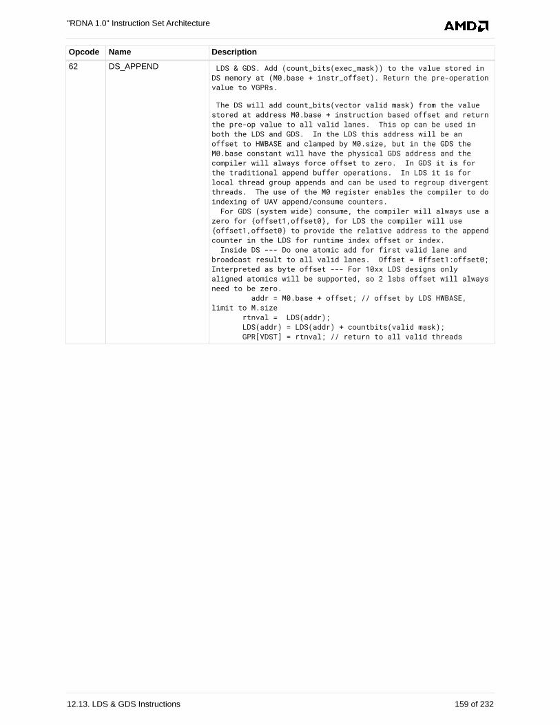
Opcode Name Description
62 DS_APPEND LDS & GDS. Add (count_bits(exec_mask)) to the value stored inDS memory at (M0.base + instr_offset). Return the pre-operationvalue to VGPRs.
The DS will add count_bits(vector valid mask) from the valuestored at address M0.base + instruction based offset and returnthe pre-op value to all valid lanes. This op can be used inboth the LDS and GDS. In the LDS this address will be anoffset to HWBASE and clamped by M0.size, but in the GDS theM0.base constant will have the physical GDS address and thecompiler will always force offset to zero. In GDS it is forthe traditional append buffer operations. In LDS it is forlocal thread group appends and can be used to regroup divergentthreads. The use of the M0 register enables the compiler to doindexing of UAV append/consume counters. For GDS (system wide) consume, the compiler will always use azero for {offset1,offset0}, for LDS the compiler will use{offset1,offset0} to provide the relative address to the appendcounter in the LDS for runtime index offset or index. Inside DS --- Do one atomic add for first valid lane andbroadcast result to all valid lanes. Offset = 0ffset1:offset0;Interpreted as byte offset --- For 10xx LDS designs onlyaligned atomics will be supported, so 2 lsbs offset will alwaysneed to be zero. addr = M0.base + offset; // offset by LDS HWBASE,limit to M.size rtnval = LDS(addr); LDS(addr) = LDS(addr) + countbits(valid mask); GPR[VDST] = rtnval; // return to all valid threads
"RDNA 1.0" Instruction Set Architecture
12.13. LDS & GDS Instructions 159 of 232
Opcode Name Description
63 DS_ORDERED_COUNT GDS-only. Add (count_bits(exec_mask)) to one of 4 dedicatedordered-count counters (aka 'packers'). Additional bits ofinstr.offset field are overloaded to hold packer-id, 'last'.
GDS Only: Intercepted by GDS and processed by ordered appendmodule. The ordered append module will queue request untilthis request wave is the oldest in the queue at which time theoldest wave request will be dispatched to the DS with an atomicadd for execution and broadcast back to ALL lanes of a wave.This is a ordered count operation and can only be called onceper issue with the release flag set. If the release flag isnot sent, the wave will have full control over the order countmodule until it sends a request with the release flag. Unlike append/consume this op needs to be sent even if thereare no valid lanes when it is issued. The GDS will add zeroand advance the tracking walker that needs to match up with thedispatch counter. The sequencer will send the following data to identify whichwave to return the result to: SQ will prepare a SH_SX_EXPCMD.gds_data.pipeline_id for theordered count to use to select the correct pipeline's trackingdata. Additionally pixel waves will use 4 counters dependingon the packer sourcing the pixel waves and generating thelaunch order. Pipeline_id = ring_id + !pixel wave type; 0 = ring0 pixel wave 1 = ring0 CS 2 = ring1 CS 3 = ring2 CS Physical_wave_id = {SH_SX_EXPCMD.se_id,SH_SX_EXPCMD.sh_id, SH_SX_EXPCMD.wave_buf_id} SH_SX_EXPCMD.gds_size from the M0.size register will containthe SPI inserted pkr_id and logical_wave_id for pixel waves andlaunch order logical wave_id for compute shaders. The pixel shader will be using four counters for eachinstance, so the pkr_id will need to be added to the gds_baseto act on the correct counter. index = find first valid (vector mask) count = src0[index][31:0]; Pkr_id = SH_SX_EXPCMD.gds_size[1:0]; gds_atomic_address[15:2] =SH_SX_EXPCMD.gds_base[15:2] will contain the dword address inthe ds for the count accumulation counter. ds_address[15:2] = SH_SX_EXPCMD.gds_base[15:2] +offset0[7:2] + (pipeline_id == 0)?Pkr_id:0 //2 new control signals Wave_release = Offset1[0]; Wave_done = offset1[1]; Pixel_wave = offset1[2]; If this control is not set, hold the crawler until wave doesan additional access with the wave_release the wave. Thisfeature allows one wavefront to issue serial access to the anyof the counters while holding off other waves. It effectivelygives the wave the ability to execute a critical code section. This logical_wave_id is created by the dispatcher andincremented with each wave that will be launched that will doan ordered append. Count = countbits (vector mask); All of the ordered appends have to fit in the bottom 128locations of GDS.
"RDNA 1.0" Instruction Set Architecture
12.13. LDS & GDS Instructions 160 of 232
Opcode Name Description
64 DS_ADD_U64 // 64bit tmp = MEM[ADDR]; MEM[ADDR] += DATA[0:1]; RETURN_DATA[0:1] = tmp.
65 DS_SUB_U64 // 64bit tmp = MEM[ADDR]; MEM[ADDR] -= DATA[0:1]; RETURN_DATA[0:1] = tmp.
66 DS_RSUB_U64 // 64bit tmp = MEM[ADDR]; MEM[ADDR] = DATA - MEM[ADDR]; RETURN_DATA = tmp. Subtraction with reversed operands.
67 DS_INC_U64 // 64bit tmp = MEM[ADDR]; MEM[ADDR] = (tmp >= DATA[0:1]) ? 0 : tmp + 1; // unsignedcompare RETURN_DATA[0:1] = tmp.
68 DS_DEC_U64 // 64bit tmp = MEM[ADDR]; MEM[ADDR] = (tmp == 0 || tmp > DATA[0:1]) ? DATA[0:1] : tmp -1; // unsigned compare RETURN_DATA[0:1] = tmp.
69 DS_MIN_I64 // 64bit tmp = MEM[ADDR]; MEM[ADDR] -= (DATA[0:1] < tmp) ? DATA[0:1] : tmp; // signedcompare RETURN_DATA[0:1] = tmp.
70 DS_MAX_I64 // 64bit tmp = MEM[ADDR]; MEM[ADDR] -= (DATA[0:1] > tmp) ? DATA[0:1] : tmp; // signedcompare RETURN_DATA[0:1] = tmp.
71 DS_MIN_U64 // 64bit tmp = MEM[ADDR]; MEM[ADDR] -= (DATA[0:1] < tmp) ? DATA[0:1] : tmp; // unsignedcompare RETURN_DATA[0:1] = tmp.
72 DS_MAX_U64 // 64bit tmp = MEM[ADDR]; MEM[ADDR] -= (DATA[0:1] > tmp) ? DATA[0:1] : tmp; // unsignedcompare RETURN_DATA[0:1] = tmp.
73 DS_AND_B64 // 64bit tmp = MEM[ADDR]; MEM[ADDR] &= DATA[0:1]; RETURN_DATA[0:1] = tmp.
74 DS_OR_B64 // 64bit tmp = MEM[ADDR]; MEM[ADDR] |= DATA[0:1]; RETURN_DATA[0:1] = tmp.
75 DS_XOR_B64 // 64bit tmp = MEM[ADDR]; MEM[ADDR] ^= DATA[0:1]; RETURN_DATA[0:1] = tmp.
"RDNA 1.0" Instruction Set Architecture
12.13. LDS & GDS Instructions 161 of 232
Opcode Name Description
76 DS_MSKOR_B64 // 64bit tmp = MEM[ADDR]; MEM[ADDR] = (MEM[ADDR] & ~DATA) | DATA2; RETURN_DATA = tmp. Masked dword OR, D0 contains the mask and D1 contains the newvalue.
77 DS_WRITE_B64 // 64bit MEM[ADDR] = DATA. Write qword.
78 DS_WRITE2_B64 // 64bit MEM[ADDR + OFFSET0 * 8] = DATA; MEM[ADDR + OFFSET1 * 8] = DATA2. Write 2 qwords.
79 DS_WRITE2ST64_B64 // 64bit MEM[ADDR + OFFSET0 * 8 * 64] = DATA; MEM[ADDR + OFFSET1 * 8 * 64] = DATA2. Write 2 qwords.
80 DS_CMPST_B64 // 64bit tmp = MEM[ADDR]; src = DATA2; cmp = DATA; MEM[ADDR] = (tmp == cmp) ? src : tmp; RETURN_DATA[0] = tmp. Compare and store. Caution, the order of src and cmp are the*opposite* of the BUFFER_ATOMIC_CMPSWAP_X2 opcode.
81 DS_CMPST_F64 // 64bit tmp = MEM[ADDR]; src = DATA2; cmp = DATA; MEM[ADDR] = (tmp == cmp) ? src : tmp; RETURN_DATA[0] = tmp. Floating point compare and store that handles NaN/INF/denormalvalues. Caution, the order of src and cmp are the *opposite*of the BUFFER_ATOMIC_FCMPSWAP_X2 opcode.
82 DS_MIN_F64 // 64bit tmp = MEM[ADDR]; src = DATA; cmp = DATA2; MEM[ADDR] = (cmp < tmp) ? src : tmp. Floating point minimum that handles NaN/INF/denormal values.Note that this opcode is slightly more general-purpose thanBUFFER_ATOMIC_FMIN_X2.
83 DS_MAX_F64 // 64bit tmp = MEM[ADDR]; src = DATA; cmp = DATA2; MEM[ADDR] = (tmp > cmp) ? src : tmp. Floating point maximum that handles NaN/INF/denormal values.Note that this opcode is slightly more general-purpose thanBUFFER_ATOMIC_FMAX_X2.
85 DS_ADD_RTN_F32 float tmp = MEM[ADDR].f32; MEM[ADDR].f32 += DATA0.f32; VDST.f32 = tmp; Floating point add that handles NaN/INF/denormal values.
96 DS_ADD_RTN_U64 // 64bit tmp = MEM[ADDR]; MEM[ADDR] += DATA[0:1]; RETURN_DATA[0:1] = tmp.
"RDNA 1.0" Instruction Set Architecture
12.13. LDS & GDS Instructions 162 of 232
Opcode Name Description
97 DS_SUB_RTN_U64 // 64bit tmp = MEM[ADDR]; MEM[ADDR] -= DATA[0:1]; RETURN_DATA[0:1] = tmp.
98 DS_RSUB_RTN_U64 // 64bit tmp = MEM[ADDR]; MEM[ADDR] = DATA - MEM[ADDR]; RETURN_DATA = tmp. Subtraction with reversed operands.
99 DS_INC_RTN_U64 // 64bit tmp = MEM[ADDR]; MEM[ADDR] = (tmp >= DATA[0:1]) ? 0 : tmp + 1; // unsignedcompare RETURN_DATA[0:1] = tmp.
100 DS_DEC_RTN_U64 // 64bit tmp = MEM[ADDR]; MEM[ADDR] = (tmp == 0 || tmp > DATA[0:1]) ? DATA[0:1] : tmp -1; // unsigned compare RETURN_DATA[0:1] = tmp.
101 DS_MIN_RTN_I64 // 64bit tmp = MEM[ADDR]; MEM[ADDR] -= (DATA[0:1] < tmp) ? DATA[0:1] : tmp; // signedcompare RETURN_DATA[0:1] = tmp.
102 DS_MAX_RTN_I64 // 64bit tmp = MEM[ADDR]; MEM[ADDR] -= (DATA[0:1] > tmp) ? DATA[0:1] : tmp; // signedcompare RETURN_DATA[0:1] = tmp.
103 DS_MIN_RTN_U64 // 64bit tmp = MEM[ADDR]; MEM[ADDR] -= (DATA[0:1] < tmp) ? DATA[0:1] : tmp; // unsignedcompare RETURN_DATA[0:1] = tmp.
104 DS_MAX_RTN_U64 // 64bit tmp = MEM[ADDR]; MEM[ADDR] -= (DATA[0:1] > tmp) ? DATA[0:1] : tmp; // unsignedcompare RETURN_DATA[0:1] = tmp.
105 DS_AND_RTN_B64 // 64bit tmp = MEM[ADDR]; MEM[ADDR] &= DATA[0:1]; RETURN_DATA[0:1] = tmp.
106 DS_OR_RTN_B64 // 64bit tmp = MEM[ADDR]; MEM[ADDR] |= DATA[0:1]; RETURN_DATA[0:1] = tmp.
107 DS_XOR_RTN_B64 // 64bit tmp = MEM[ADDR]; MEM[ADDR] ^= DATA[0:1]; RETURN_DATA[0:1] = tmp.
108 DS_MSKOR_RTN_B64 // 64bit tmp = MEM[ADDR]; MEM[ADDR] = (MEM[ADDR] & ~DATA) | DATA2; RETURN_DATA = tmp. Masked dword OR, D0 contains the mask and D1 contains the newvalue.
"RDNA 1.0" Instruction Set Architecture
12.13. LDS & GDS Instructions 163 of 232
Opcode Name Description
109 DS_WRXCHG_RTN_B64 tmp = MEM[ADDR]; MEM[ADDR] = DATA; RETURN_DATA = tmp. Write-exchange operation.
110 DS_WRXCHG2_RTN_B64
Write-exchange 2 separate qwords.
111 DS_WRXCHG2ST64_RTN_B64
Write-exchange 2 qwords with a stride of 64 qwords.
112 DS_CMPST_RTN_B64 // 64bit tmp = MEM[ADDR]; src = DATA2; cmp = DATA; MEM[ADDR] = (tmp == cmp) ? src : tmp; RETURN_DATA[0] = tmp. Compare and store. Caution, the order of src and cmp are the*opposite* of the BUFFER_ATOMIC_CMPSWAP_X2 opcode.
113 DS_CMPST_RTN_F64 // 64bit tmp = MEM[ADDR]; src = DATA2; cmp = DATA; MEM[ADDR] = (tmp == cmp) ? src : tmp; RETURN_DATA[0] = tmp. Floating point compare and store that handles NaN/INF/denormalvalues. Caution, the order of src and cmp are the *opposite*of the BUFFER_ATOMIC_FCMPSWAP_X2 opcode.
114 DS_MIN_RTN_F64 // 64bit tmp = MEM[ADDR]; src = DATA; cmp = DATA2; MEM[ADDR] = (cmp < tmp) ? src : tmp. Floating point minimum that handles NaN/INF/denormal values.Note that this opcode is slightly more general-purpose thanBUFFER_ATOMIC_FMIN_X2.
115 DS_MAX_RTN_F64 // 64bit tmp = MEM[ADDR]; src = DATA; cmp = DATA2; MEM[ADDR] = (tmp > cmp) ? src : tmp. Floating point maximum that handles NaN/INF/denormal values.Note that this opcode is slightly more general-purpose thanBUFFER_ATOMIC_FMAX_X2.
118 DS_READ_B64 RETURN_DATA = MEM[ADDR]. Read 1 qword.
119 DS_READ2_B64 RETURN_DATA[0] = MEM[ADDR + OFFSET0 * 8]; RETURN_DATA[1] = MEM[ADDR + OFFSET1 * 8]. Read 2 qwords.
120 DS_READ2ST64_B64 RETURN_DATA[0] = MEM[ADDR + OFFSET0 * 8 * 64]; RETURN_DATA[1] = MEM[ADDR + OFFSET1 * 8 * 64]. Read 2 qwords.
126 DS_CONDXCHG32_RTN_B64
Conditional write exchange.
160 DS_WRITE_B8_D16_HI MEM[ADDR] = DATA[23:16]. Byte write in to high word.
161 DS_WRITE_B16_D16_HI MEM[ADDR] = DATA[31:16]. Short write in to high word.
"RDNA 1.0" Instruction Set Architecture
12.13. LDS & GDS Instructions 164 of 232
Opcode Name Description
162 DS_READ_U8_D16 RETURN_DATA[15:0] = {8'h0,MEM[ADDR][7:0]}. Unsigned byte read with masked return to lower word.
163 DS_READ_U8_D16_HI RETURN_DATA[31:16] = {8'h0,MEM[ADDR][7:0]}. Unsigned byte read with masked return to upper word.
164 DS_READ_I8_D16 RETURN_DATA[15:0] = signext(MEM[ADDR][7:0]). Signed byte read with masked return to lower word.
165 DS_READ_I8_D16_HI RETURN_DATA[31:16] = signext(MEM[ADDR][7:0]). Signed byte read with masked return to upper word.
166 DS_READ_U16_D16 RETURN_DATA[15:0] = MEM[ADDR][15:0]. Unsigned short read with masked return to lower word.
167 DS_READ_U16_D16_HI RETURN_DATA[31:0] = MEM[ADDR][15:0]. Unsigned short read with masked return to upper word.
176 DS_WRITE_ADDTID_B32 LDS_GS[LDS_BASE + {OFFSET1,OFFSET0} + M0[15:0] + TID*4].u32 =VGPR[DATA0].u32 Write dword.
177 DS_READ_ADDTID_B32 VGPR[VDST].u32 = LDS_GS[LDS_BASE + {OFFSET1,OFFSET0} +M0[15:0] + TID*4].u32 Dword read.
178 DS_PERMUTE_B32 // VGPR[index][thread_id] is the VGPR RAM // VDST, ADDR and DATA0 are from the microcode DS encoding tmp[0..63] = 0 for i in 0..63 do // If a source thread is disabled, it will notpropagate data. next if !EXEC[i] // ADDR needs to be divided by 4. // High-order bits are ignored. dst_lane = floor((VGPR[ADDR][i] + OFFSET) / 4)mod 64 tmp[dst_lane] = VGPR[DATA0][i] endfor // Copy data into destination VGPRs. If multiple sources // select the same destination thread, the highest-numbered // source thread wins. for i in 0..63 do next if !EXEC[i] VGPR[VDST][i] = tmp[i] endfor Forward permute. This does not access LDS memory and may becalled even if no LDS memory is allocated to the wave. It usesLDS hardware to implement an arbitrary swizzle across threadsin a wavefront. Note the address passed in is the thread ID multiplied by 4.This is due to a limitation in the DS hardware design. If multiple sources map to the same destination lane, standardLDS arbitration rules determine which write wins. See also DS_BPERMUTE_B32. Examples (simplified 4-thread wavefronts):
VGPR[SRC0] = { A, B, C, D } VGPR[ADDR] = { 0, 0, 12, 4 } EXEC = 0xF, OFFSET = 0 VGPR[VDST] := { B, D, 0, C }
VGPR[SRC0] = { A, B, C, D } VGPR[ADDR] = { 0, 0, 12, 4 } EXEC = 0xA, OFFSET = 0 VGPR[VDST] := { -, D, -, 0 }
"RDNA 1.0" Instruction Set Architecture
12.13. LDS & GDS Instructions 165 of 232
Opcode Name Description
179 DS_BPERMUTE_B32 // VGPR[index][thread_id] is the VGPR RAM // VDST, ADDR and DATA0 are from the microcode DS encoding tmp[0..63] = 0 for i in 0..63 do // ADDR needs to be divided by 4. // High-order bits are ignored. src_lane = floor((VGPR[ADDR][i] + OFFSET) / 4)mod 64 // EXEC is applied to the source VGPR reads. next if !EXEC[src_lane] tmp[i] = VGPR[DATA0][src_lane] endfor // Copy data into destination VGPRs. Some source // data may be broadcast to multiple lanes. for i in 0..63 do next if !EXEC[i] VGPR[VDST][i] = tmp[i] endfor Backward permute. This does not access LDS memory and may becalled even if no LDS memory is allocated to the wave. It usesLDS hardware to implement an arbitrary swizzle across threadsin a wavefront. Note the address passed in is the thread ID multiplied by 4.This is due to a limitation in the DS hardware design. Note that EXEC mask is applied to both VGPR read and write.If src_lane selects a disabled thread, zero will be returned. See also DS_PERMUTE_B32. Examples (simplified 4-thread wavefronts):
VGPR[SRC0] = { A, B, C, D } VGPR[ADDR] = { 0, 0, 12, 4 } EXEC = 0xF, OFFSET = 0 VGPR[VDST] := { A, A, D, B }
VGPR[SRC0] = { A, B, C, D } VGPR[ADDR] = { 0, 0, 12, 4 } EXEC = 0xA, OFFSET = 0 VGPR[VDST] := { -, 0, -, B }
222 DS_WRITE_B96 {MEM[ADDR + 8], MEM[ADDR + 4], MEM[ADDR]} = DATA[95:0]. Tri-dword write.
223 DS_WRITE_B128 {MEM[ADDR + 12], MEM[ADDR + 8], MEM[ADDR + 4], MEM[ADDR]} =DATA[127:0]. Quad-dword write.
254 DS_READ_B96 Tri-dword read.
255 DS_READ_B128 Quad-dword read.
12.13.1. DS_SWIZZLE_B32 Details
Dword swizzle, no data is written to LDS memory.Swizzles input thread data based on offset mask and returns; note does not read or write theDS memory banks.Note that reading from an invalid thread results in 0x0.This opcode supports two special modes, FFT and rotate, plus two basic modes which swizzle ingroups of 4 or 32 consecutive threads.The FFT mode (offset >= 0xe000) swizzles the input based on offset[4:0] to support FFTcalculation. Example swizzles using input {1, 2, ... 20} are:
"RDNA 1.0" Instruction Set Architecture
12.13. LDS & GDS Instructions 166 of 232
Offset[4:0]: Swizzle0x00: {1,11,9,19,5,15,d,1d,3,13,b,1b,7,17,f,1f,2,12,a,1a,6,16,e,1e,4,14,c,1c,8,18,10,20}0x10: {1,9,5,d,3,b,7,f,2,a,6,e,4,c,8,10,11,19,15,1d,13,1b,17,1f,12,1a,16,1e,14,1c,18,20}0x1f: No swizzleThe rotate mode (offset >= 0xc000 and offset < 0xe000) rotates the input either left(offset[10] == 0) or right (offset[10] == 1) a number of threads equal to offset[9:5]. Therotate mode also uses a mask value which can alter the rotate result. For example, mask == 1will swap the odd threads across every other even thread (rotate left), or even threads acrossevery other odd thread (rotate right).Offset[9:5]: Swizzle0x01, mask=0, rotate left:{2,3,4,5,6,7,8,9,a,b,c,d,e,f,10,11,12,13,14,15,16,17,18,19,1a,1b,1c,1d,1e,1f,20,1}0x01, mask=0, rotate right:{20,1,2,3,4,5,6,7,8,9,a,b,c,d,e,f,10,11,12,13,14,15,16,17,18,19,1a,1b,1c,1d,1e,1f}0x01, mask=1, rotate left:{2,1,4,7,6,5,8,b,a,9,c,f,e,d,10,13,12,11,14,17,16,15,18,1b,1a,19,1c,1f,1e,1d,20,3}0x01, mask=1, rotate right:{1e,1,4,3,2,5,8,7,6,9,c,b,a,d,10,f,e,11,14,13,12,15,18,17,16,19,1c,1b,1a,1d,20,1f}If offset < 0xc000, one of the basic swizzle modes is used based on offset[15]. If offset[15]== 1, groups of 4 consecutive threads are swizzled together. If offset[15] == 0, all 32threads are swizzled together. The first basic swizzle mode (when offset[15] == 1) allows fulldata sharing between a group of 4 consecutive threads. Any thread within the group of 4 canget data from any other thread within the group of 4, specified by the corresponding offsetbits --- [1:0] for the first thread, [3:2] for the second thread, [5:4] for the third thread,[7:6] for the fourth thread. Note that the offset bits apply to all groups of 4 within awavefront; thus if offset[1:0] == 1, then thread0 will grab thread1, thread4 will grabthread5, etc.The second basic swizzle mode (when offset[15] == 0) allows limited data sharing between 32consecutive threads. In this case, the offset is used to specify a 5-bit xor-mask, 5-bit or-mask, and 5-bit and-mask used to generate a thread mapping. Note that the offset bits apply toeach group of 32 within a wavefront. The details of the thread mapping are listed below. Someexample usages:SWAPX16 : xor_mask = 0x10, or_mask = 0x00, and_mask = 0x1fSWAPX8 : xor_mask = 0x08, or_mask = 0x00, and_mask = 0x1fSWAPX4 : xor_mask = 0x04, or_mask = 0x00, and_mask = 0x1fSWAPX2 : xor_mask = 0x02, or_mask = 0x00, and_mask = 0x1fSWAPX1 : xor_mask = 0x01, or_mask = 0x00, and_mask = 0x1fREVERSEX32 : xor_mask = 0x1f, or_mask = 0x00, and_mask = 0x1fREVERSEX16 : xor_mask = 0x0f, or_mask = 0x00, and_mask = 0x1fREVERSEX8 : xor_mask = 0x07, or_mask = 0x00, and_mask = 0x1fREVERSEX4 : xor_mask = 0x03, or_mask = 0x00, and_mask = 0x1fREVERSEX2 : xor_mask = 0x01 or_mask = 0x00, and_mask = 0x1fBCASTX32: xor_mask = 0x00, or_mask = thread, and_mask = 0x00BCASTX16: xor_mask = 0x00, or_mask = thread, and_mask = 0x10BCASTX8: xor_mask = 0x00, or_mask = thread, and_mask = 0x18BCASTX4: xor_mask = 0x00, or_mask = thread, and_mask = 0x1cBCASTX2: xor_mask = 0x00, or_mask = thread, and_mask = 0x1ePseudocode follows: offset = offset1:offset0;if (offset >= 0xe000) { // FFT decomposition mask = offset[4:0]; for (i = 0; i < 64; i++) { j = reverse_bits(i & 0x1f); j = (j >> count_ones(mask));
"RDNA 1.0" Instruction Set Architecture
12.13. LDS & GDS Instructions 167 of 232
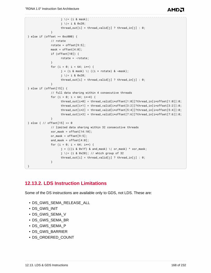
j \|= (i & mask); j \|= i & 0x20; thread_out[i] = thread_valid[j] ? thread_in[j] : 0; }} else if (offset >= 0xc000) { // rotate rotate = offset[9:5]; mask = offset[4:0]; if (offset[10]) { rotate = -rotate; } for (i = 0; i < 64; i++) { j = (i & mask) \| ((i + rotate) & ~mask); j \|= i & 0x20; thread_out[i] = thread_valid[j] ? thread_in[j] : 0; }} else if (offset[15]) { // full data sharing within 4 consecutive threads for (i = 0; i < 64; i+=4) { thread_out[i+0] = thread_valid[i+offset[1:0]]?thread_in[i+offset[1:0]]:0; thread_out[i+1] = thread_valid[i+offset[3:2]]?thread_in[i+offset[3:2]]:0; thread_out[i+2] = thread_valid[i+offset[5:4]]?thread_in[i+offset[5:4]]:0; thread_out[i+3] = thread_valid[i+offset[7:6]]?thread_in[i+offset[7:6]]:0; }} else { // offset[15] == 0 // limited data sharing within 32 consecutive threads xor_mask = offset[14:10]; or_mask = offset[9:5]; and_mask = offset[4:0]; for (i = 0; i < 64; i++) { j = (((i & 0x1f) & and_mask) \| or_mask) ^ xor_mask; j \|= (i & 0x20); // which group of 32 thread_out[i] = thread_valid[j] ? thread_in[j] : 0; }}
12.13.2. LDS Instruction Limitations
Some of the DS instructions are available only to GDS, not LDS. These are:
• DS_GWS_SEMA_RELEASE_ALL
• DS_GWS_INIT
• DS_GWS_SEMA_V
• DS_GWS_SEMA_BR
• DS_GWS_SEMA_P
• DS_GWS_BARRIER
• DS_ORDERED_COUNT
"RDNA 1.0" Instruction Set Architecture
12.13. LDS & GDS Instructions 168 of 232
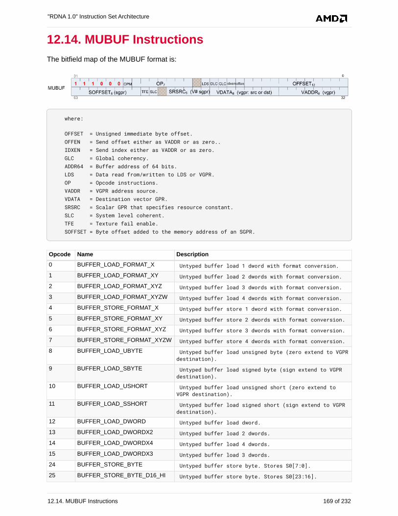
12.14. MUBUF Instructions
The bitfield map of the MUBUF format is:
where:
OFFSET = Unsigned immediate byte offset. OFFEN = Send offset either as VADDR or as zero.. IDXEN = Send index either as VADDR or as zero. GLC = Global coherency. ADDR64 = Buffer address of 64 bits. LDS = Data read from/written to LDS or VGPR. OP = Opcode instructions. VADDR = VGPR address source. VDATA = Destination vector GPR. SRSRC = Scalar GPR that specifies resource constant. SLC = System level coherent. TFE = Texture fail enable. SOFFSET = Byte offset added to the memory address of an SGPR.
Opcode Name Description
0 BUFFER_LOAD_FORMAT_X Untyped buffer load 1 dword with format conversion.
1 BUFFER_LOAD_FORMAT_XY Untyped buffer load 2 dwords with format conversion.
2 BUFFER_LOAD_FORMAT_XYZ Untyped buffer load 3 dwords with format conversion.
3 BUFFER_LOAD_FORMAT_XYZW Untyped buffer load 4 dwords with format conversion.
4 BUFFER_STORE_FORMAT_X Untyped buffer store 1 dword with format conversion.
5 BUFFER_STORE_FORMAT_XY Untyped buffer store 2 dwords with format conversion.
6 BUFFER_STORE_FORMAT_XYZ Untyped buffer store 3 dwords with format conversion.
7 BUFFER_STORE_FORMAT_XYZW Untyped buffer store 4 dwords with format conversion.
8 BUFFER_LOAD_UBYTE Untyped buffer load unsigned byte (zero extend to VGPRdestination).
9 BUFFER_LOAD_SBYTE Untyped buffer load signed byte (sign extend to VGPRdestination).
10 BUFFER_LOAD_USHORT Untyped buffer load unsigned short (zero extend toVGPR destination).
11 BUFFER_LOAD_SSHORT Untyped buffer load signed short (sign extend to VGPRdestination).
12 BUFFER_LOAD_DWORD Untyped buffer load dword.
13 BUFFER_LOAD_DWORDX2 Untyped buffer load 2 dwords.
14 BUFFER_LOAD_DWORDX4 Untyped buffer load 4 dwords.
15 BUFFER_LOAD_DWORDX3 Untyped buffer load 3 dwords.
24 BUFFER_STORE_BYTE Untyped buffer store byte. Stores S0[7:0].
25 BUFFER_STORE_BYTE_D16_HI Untyped buffer store byte. Stores S0[23:16].
"RDNA 1.0" Instruction Set Architecture
12.14. MUBUF Instructions 169 of 232
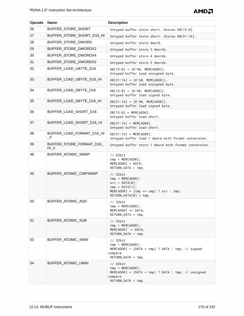
Opcode Name Description
26 BUFFER_STORE_SHORT Untyped buffer store short. Stores S0[15:0].
27 BUFFER_STORE_SHORT_D16_HI Untyped buffer store short. Stores S0[31:16].
28 BUFFER_STORE_DWORD Untyped buffer store dword.
29 BUFFER_STORE_DWORDX2 Untyped buffer store 2 dwords.
30 BUFFER_STORE_DWORDX4 Untyped buffer store 4 dwords.
31 BUFFER_STORE_DWORDX3 Untyped buffer store 3 dwords.
32 BUFFER_LOAD_UBYTE_D16 D0[15:0] = {8'h0, MEM[ADDR]}. Untyped buffer load unsigned byte.
33 BUFFER_LOAD_UBYTE_D16_HI D0[31:16] = {8'h0, MEM[ADDR]}. Untyped buffer load unsigned byte.
34 BUFFER_LOAD_SBYTE_D16 D0[15:0] = {8'h0, MEM[ADDR]}. Untyped buffer load signed byte.
35 BUFFER_LOAD_SBYTE_D16_HI D0[31:16] = {8'h0, MEM[ADDR]}. Untyped buffer load signed byte.
36 BUFFER_LOAD_SHORT_D16 D0[15:0] = MEM[ADDR]. Untyped buffer load short.
37 BUFFER_LOAD_SHORT_D16_HI D0[31:16] = MEM[ADDR]. Untyped buffer load short.
38 BUFFER_LOAD_FORMAT_D16_HI_X
D0[31:16] = MEM[ADDR]. Untyped buffer load 1 dword with format conversion.
39 BUFFER_STORE_FORMAT_D16_HI_X
Untyped buffer store 1 dword with format conversion.
48 BUFFER_ATOMIC_SWAP // 32bit tmp = MEM[ADDR]; MEM[ADDR] = DATA; RETURN_DATA = tmp.
49 BUFFER_ATOMIC_CMPSWAP // 32bit tmp = MEM[ADDR]; src = DATA[0]; cmp = DATA[1]; MEM[ADDR] = (tmp == cmp) ? src : tmp; RETURN_DATA[0] = tmp.
50 BUFFER_ATOMIC_ADD // 32bit tmp = MEM[ADDR]; MEM[ADDR] += DATA; RETURN_DATA = tmp.
51 BUFFER_ATOMIC_SUB // 32bit tmp = MEM[ADDR]; MEM[ADDR] -= DATA; RETURN_DATA = tmp.
53 BUFFER_ATOMIC_SMIN // 32bit tmp = MEM[ADDR]; MEM[ADDR] = (DATA < tmp) ? DATA : tmp; // signedcompare RETURN_DATA = tmp.
54 BUFFER_ATOMIC_UMIN // 32bit tmp = MEM[ADDR]; MEM[ADDR] = (DATA < tmp) ? DATA : tmp; // unsignedcompare RETURN_DATA = tmp.
"RDNA 1.0" Instruction Set Architecture
12.14. MUBUF Instructions 170 of 232
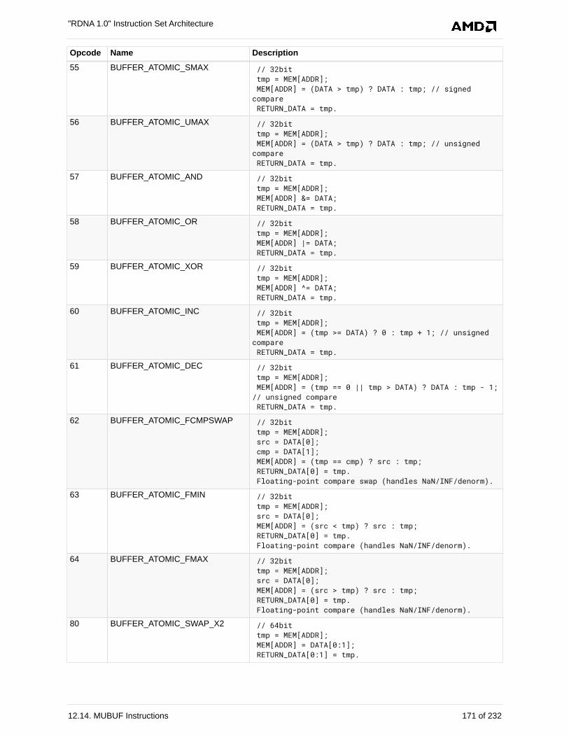
Opcode Name Description
55 BUFFER_ATOMIC_SMAX // 32bit tmp = MEM[ADDR]; MEM[ADDR] = (DATA > tmp) ? DATA : tmp; // signedcompare RETURN_DATA = tmp.
56 BUFFER_ATOMIC_UMAX // 32bit tmp = MEM[ADDR]; MEM[ADDR] = (DATA > tmp) ? DATA : tmp; // unsignedcompare RETURN_DATA = tmp.
57 BUFFER_ATOMIC_AND // 32bit tmp = MEM[ADDR]; MEM[ADDR] &= DATA; RETURN_DATA = tmp.
58 BUFFER_ATOMIC_OR // 32bit tmp = MEM[ADDR]; MEM[ADDR] |= DATA; RETURN_DATA = tmp.
59 BUFFER_ATOMIC_XOR // 32bit tmp = MEM[ADDR]; MEM[ADDR] ^= DATA; RETURN_DATA = tmp.
60 BUFFER_ATOMIC_INC // 32bit tmp = MEM[ADDR]; MEM[ADDR] = (tmp >= DATA) ? 0 : tmp + 1; // unsignedcompare RETURN_DATA = tmp.
61 BUFFER_ATOMIC_DEC // 32bit tmp = MEM[ADDR]; MEM[ADDR] = (tmp == 0 || tmp > DATA) ? DATA : tmp - 1;// unsigned compare RETURN_DATA = tmp.
62 BUFFER_ATOMIC_FCMPSWAP // 32bit tmp = MEM[ADDR]; src = DATA[0]; cmp = DATA[1]; MEM[ADDR] = (tmp == cmp) ? src : tmp; RETURN_DATA[0] = tmp. Floating-point compare swap (handles NaN/INF/denorm).
63 BUFFER_ATOMIC_FMIN // 32bit tmp = MEM[ADDR]; src = DATA[0]; MEM[ADDR] = (src < tmp) ? src : tmp; RETURN_DATA[0] = tmp. Floating-point compare (handles NaN/INF/denorm).
64 BUFFER_ATOMIC_FMAX // 32bit tmp = MEM[ADDR]; src = DATA[0]; MEM[ADDR] = (src > tmp) ? src : tmp; RETURN_DATA[0] = tmp. Floating-point compare (handles NaN/INF/denorm).
80 BUFFER_ATOMIC_SWAP_X2 // 64bit tmp = MEM[ADDR]; MEM[ADDR] = DATA[0:1]; RETURN_DATA[0:1] = tmp.
"RDNA 1.0" Instruction Set Architecture
12.14. MUBUF Instructions 171 of 232
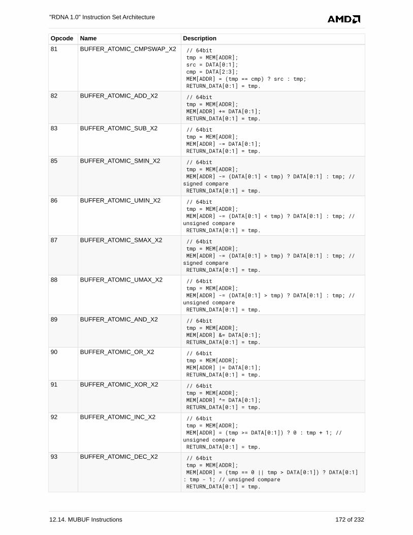
Opcode Name Description
81 BUFFER_ATOMIC_CMPSWAP_X2 // 64bit tmp = MEM[ADDR]; src = DATA[0:1]; cmp = DATA[2:3]; MEM[ADDR] = (tmp == cmp) ? src : tmp; RETURN_DATA[0:1] = tmp.
82 BUFFER_ATOMIC_ADD_X2 // 64bit tmp = MEM[ADDR]; MEM[ADDR] += DATA[0:1]; RETURN_DATA[0:1] = tmp.
83 BUFFER_ATOMIC_SUB_X2 // 64bit tmp = MEM[ADDR]; MEM[ADDR] -= DATA[0:1]; RETURN_DATA[0:1] = tmp.
85 BUFFER_ATOMIC_SMIN_X2 // 64bit tmp = MEM[ADDR]; MEM[ADDR] -= (DATA[0:1] < tmp) ? DATA[0:1] : tmp; //signed compare RETURN_DATA[0:1] = tmp.
86 BUFFER_ATOMIC_UMIN_X2 // 64bit tmp = MEM[ADDR]; MEM[ADDR] -= (DATA[0:1] < tmp) ? DATA[0:1] : tmp; //unsigned compare RETURN_DATA[0:1] = tmp.
87 BUFFER_ATOMIC_SMAX_X2 // 64bit tmp = MEM[ADDR]; MEM[ADDR] -= (DATA[0:1] > tmp) ? DATA[0:1] : tmp; //signed compare RETURN_DATA[0:1] = tmp.
88 BUFFER_ATOMIC_UMAX_X2 // 64bit tmp = MEM[ADDR]; MEM[ADDR] -= (DATA[0:1] > tmp) ? DATA[0:1] : tmp; //unsigned compare RETURN_DATA[0:1] = tmp.
89 BUFFER_ATOMIC_AND_X2 // 64bit tmp = MEM[ADDR]; MEM[ADDR] &= DATA[0:1]; RETURN_DATA[0:1] = tmp.
90 BUFFER_ATOMIC_OR_X2 // 64bit tmp = MEM[ADDR]; MEM[ADDR] |= DATA[0:1]; RETURN_DATA[0:1] = tmp.
91 BUFFER_ATOMIC_XOR_X2 // 64bit tmp = MEM[ADDR]; MEM[ADDR] ^= DATA[0:1]; RETURN_DATA[0:1] = tmp.
92 BUFFER_ATOMIC_INC_X2 // 64bit tmp = MEM[ADDR]; MEM[ADDR] = (tmp >= DATA[0:1]) ? 0 : tmp + 1; //unsigned compare RETURN_DATA[0:1] = tmp.
93 BUFFER_ATOMIC_DEC_X2 // 64bit tmp = MEM[ADDR]; MEM[ADDR] = (tmp == 0 || tmp > DATA[0:1]) ? DATA[0:1]: tmp - 1; // unsigned compare RETURN_DATA[0:1] = tmp.
"RDNA 1.0" Instruction Set Architecture
12.14. MUBUF Instructions 172 of 232
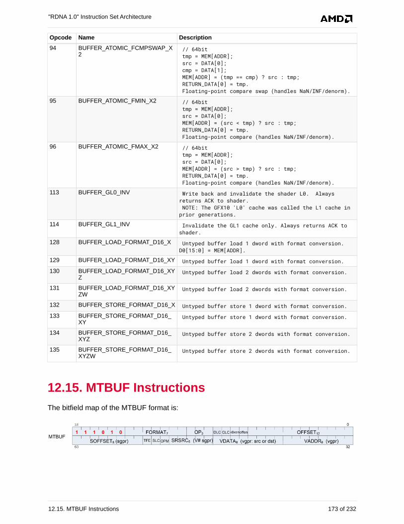
Opcode Name Description
94 BUFFER_ATOMIC_FCMPSWAP_X2
// 64bit tmp = MEM[ADDR]; src = DATA[0]; cmp = DATA[1]; MEM[ADDR] = (tmp == cmp) ? src : tmp; RETURN_DATA[0] = tmp. Floating-point compare swap (handles NaN/INF/denorm).
95 BUFFER_ATOMIC_FMIN_X2 // 64bit tmp = MEM[ADDR]; src = DATA[0]; MEM[ADDR] = (src < tmp) ? src : tmp; RETURN_DATA[0] = tmp. Floating-point compare (handles NaN/INF/denorm).
96 BUFFER_ATOMIC_FMAX_X2 // 64bit tmp = MEM[ADDR]; src = DATA[0]; MEM[ADDR] = (src > tmp) ? src : tmp; RETURN_DATA[0] = tmp. Floating-point compare (handles NaN/INF/denorm).
113 BUFFER_GL0_INV Write back and invalidate the shader L0. Alwaysreturns ACK to shader. NOTE: The GFX10 'L0' cache was called the L1 cache inprior generations.
114 BUFFER_GL1_INV Invalidate the GL1 cache only. Always returns ACK toshader.
128 BUFFER_LOAD_FORMAT_D16_X Untyped buffer load 1 dword with format conversion.D0[15:0] = MEM[ADDR].
129 BUFFER_LOAD_FORMAT_D16_XY Untyped buffer load 1 dword with format conversion.
130 BUFFER_LOAD_FORMAT_D16_XYZ
Untyped buffer load 2 dwords with format conversion.
131 BUFFER_LOAD_FORMAT_D16_XYZW
Untyped buffer load 2 dwords with format conversion.
132 BUFFER_STORE_FORMAT_D16_X Untyped buffer store 1 dword with format conversion.
133 BUFFER_STORE_FORMAT_D16_XY
Untyped buffer store 1 dword with format conversion.
134 BUFFER_STORE_FORMAT_D16_XYZ
Untyped buffer store 2 dwords with format conversion.
135 BUFFER_STORE_FORMAT_D16_XYZW
Untyped buffer store 2 dwords with format conversion.
12.15. MTBUF Instructions
The bitfield map of the MTBUF format is:
"RDNA 1.0" Instruction Set Architecture
12.15. MTBUF Instructions 173 of 232
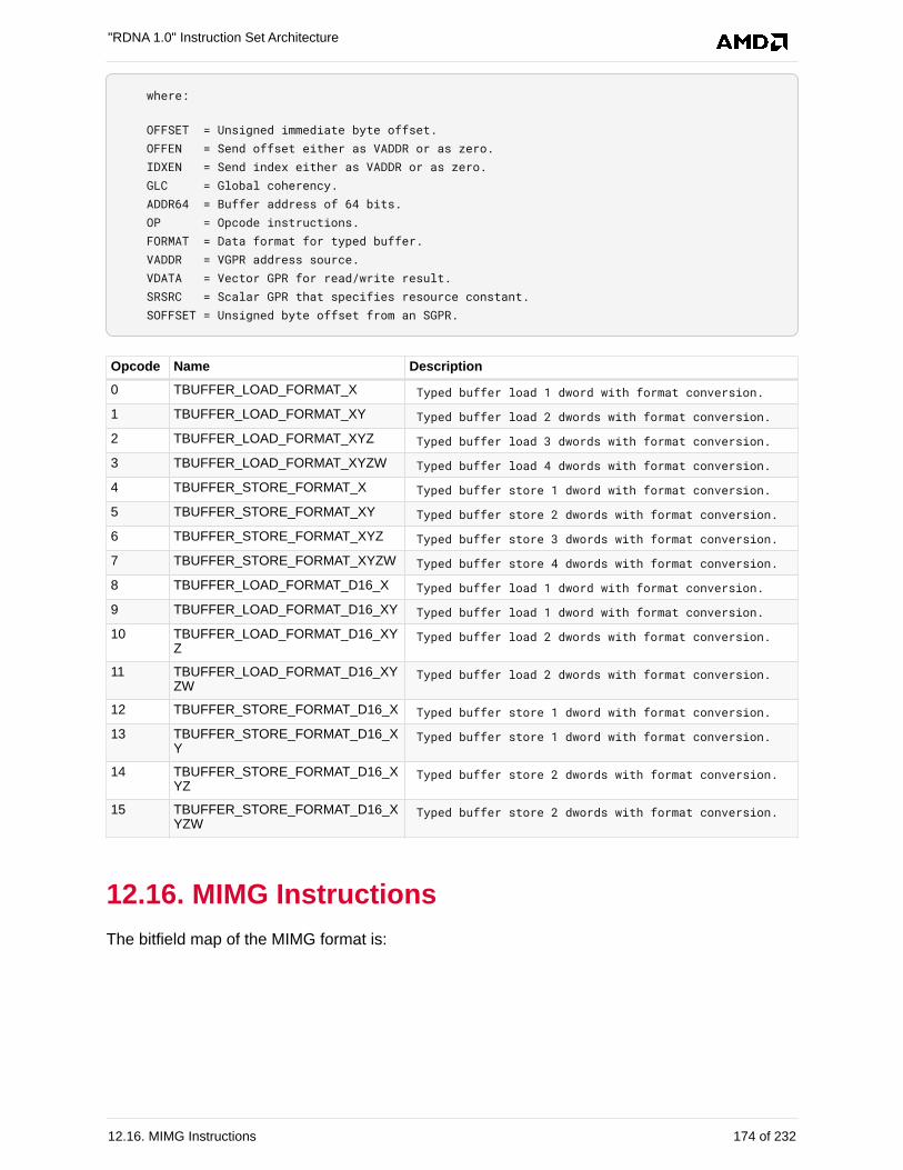
where:
OFFSET = Unsigned immediate byte offset. OFFEN = Send offset either as VADDR or as zero. IDXEN = Send index either as VADDR or as zero. GLC = Global coherency. ADDR64 = Buffer address of 64 bits. OP = Opcode instructions. FORMAT = Data format for typed buffer. VADDR = VGPR address source. VDATA = Vector GPR for read/write result. SRSRC = Scalar GPR that specifies resource constant. SOFFSET = Unsigned byte offset from an SGPR.
Opcode Name Description
0 TBUFFER_LOAD_FORMAT_X Typed buffer load 1 dword with format conversion.
1 TBUFFER_LOAD_FORMAT_XY Typed buffer load 2 dwords with format conversion.
2 TBUFFER_LOAD_FORMAT_XYZ Typed buffer load 3 dwords with format conversion.
3 TBUFFER_LOAD_FORMAT_XYZW Typed buffer load 4 dwords with format conversion.
4 TBUFFER_STORE_FORMAT_X Typed buffer store 1 dword with format conversion.
5 TBUFFER_STORE_FORMAT_XY Typed buffer store 2 dwords with format conversion.
6 TBUFFER_STORE_FORMAT_XYZ Typed buffer store 3 dwords with format conversion.
7 TBUFFER_STORE_FORMAT_XYZW Typed buffer store 4 dwords with format conversion.
8 TBUFFER_LOAD_FORMAT_D16_X Typed buffer load 1 dword with format conversion.
9 TBUFFER_LOAD_FORMAT_D16_XY Typed buffer load 1 dword with format conversion.
10 TBUFFER_LOAD_FORMAT_D16_XYZ
Typed buffer load 2 dwords with format conversion.
11 TBUFFER_LOAD_FORMAT_D16_XYZW
Typed buffer load 2 dwords with format conversion.
12 TBUFFER_STORE_FORMAT_D16_X Typed buffer store 1 dword with format conversion.
13 TBUFFER_STORE_FORMAT_D16_XY
Typed buffer store 1 dword with format conversion.
14 TBUFFER_STORE_FORMAT_D16_XYZ
Typed buffer store 2 dwords with format conversion.
15 TBUFFER_STORE_FORMAT_D16_XYZW
Typed buffer store 2 dwords with format conversion.
12.16. MIMG Instructions
The bitfield map of the MIMG format is:
"RDNA 1.0" Instruction Set Architecture
12.16. MIMG Instructions 174 of 232
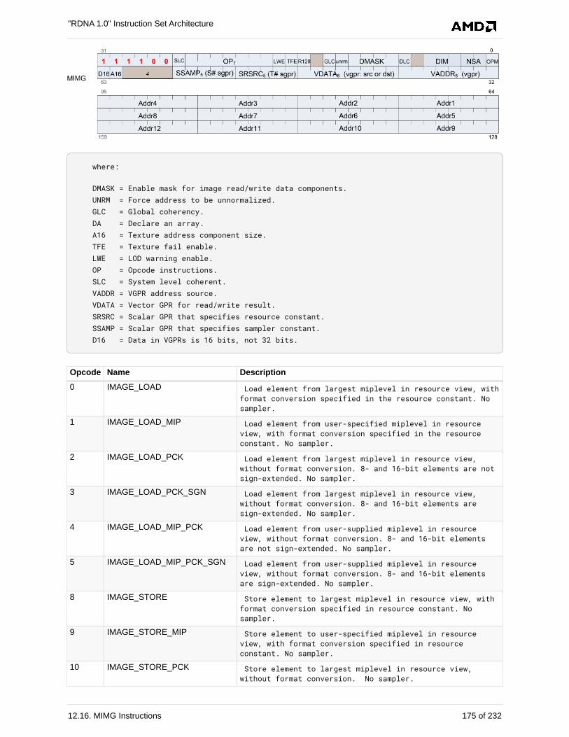
where:
DMASK = Enable mask for image read/write data components. UNRM = Force address to be unnormalized. GLC = Global coherency. DA = Declare an array. A16 = Texture address component size. TFE = Texture fail enable. LWE = LOD warning enable. OP = Opcode instructions. SLC = System level coherent. VADDR = VGPR address source. VDATA = Vector GPR for read/write result. SRSRC = Scalar GPR that specifies resource constant. SSAMP = Scalar GPR that specifies sampler constant. D16 = Data in VGPRs is 16 bits, not 32 bits.
Opcode Name Description
0 IMAGE_LOAD Load element from largest miplevel in resource view, withformat conversion specified in the resource constant. Nosampler.
1 IMAGE_LOAD_MIP Load element from user-specified miplevel in resourceview, with format conversion specified in the resourceconstant. No sampler.
2 IMAGE_LOAD_PCK Load element from largest miplevel in resource view,without format conversion. 8- and 16-bit elements are notsign-extended. No sampler.
3 IMAGE_LOAD_PCK_SGN Load element from largest miplevel in resource view,without format conversion. 8- and 16-bit elements aresign-extended. No sampler.
4 IMAGE_LOAD_MIP_PCK Load element from user-supplied miplevel in resourceview, without format conversion. 8- and 16-bit elementsare not sign-extended. No sampler.
5 IMAGE_LOAD_MIP_PCK_SGN Load element from user-supplied miplevel in resourceview, without format conversion. 8- and 16-bit elementsare sign-extended. No sampler.
8 IMAGE_STORE Store element to largest miplevel in resource view, withformat conversion specified in resource constant. Nosampler.
9 IMAGE_STORE_MIP Store element to user-specified miplevel in resourceview, with format conversion specified in resourceconstant. No sampler.
10 IMAGE_STORE_PCK Store element to largest miplevel in resource view,without format conversion. No sampler.
"RDNA 1.0" Instruction Set Architecture
12.16. MIMG Instructions 175 of 232
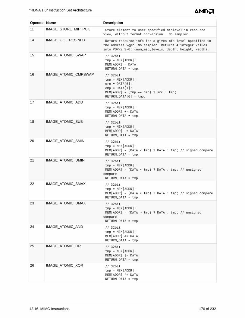
Opcode Name Description
11 IMAGE_STORE_MIP_PCK Store element to user-specified miplevel in resourceview, without format conversion. No sampler.
14 IMAGE_GET_RESINFO Return resource info for a given mip level specified inthe address vgpr. No sampler. Returns 4 integer valuesinto VGPRs 3-0: {num_mip_levels, depth, height, width}.
15 IMAGE_ATOMIC_SWAP // 32bit tmp = MEM[ADDR]; MEM[ADDR] = DATA; RETURN_DATA = tmp.
16 IMAGE_ATOMIC_CMPSWAP // 32bit tmp = MEM[ADDR]; src = DATA[0]; cmp = DATA[1]; MEM[ADDR] = (tmp == cmp) ? src : tmp; RETURN_DATA[0] = tmp.
17 IMAGE_ATOMIC_ADD // 32bit tmp = MEM[ADDR]; MEM[ADDR] += DATA; RETURN_DATA = tmp.
18 IMAGE_ATOMIC_SUB // 32bit tmp = MEM[ADDR]; MEM[ADDR] -= DATA; RETURN_DATA = tmp.
20 IMAGE_ATOMIC_SMIN // 32bit tmp = MEM[ADDR]; MEM[ADDR] = (DATA < tmp) ? DATA : tmp; // signed compare RETURN_DATA = tmp.
21 IMAGE_ATOMIC_UMIN // 32bit tmp = MEM[ADDR]; MEM[ADDR] = (DATA < tmp) ? DATA : tmp; // unsignedcompare RETURN_DATA = tmp.
22 IMAGE_ATOMIC_SMAX // 32bit tmp = MEM[ADDR]; MEM[ADDR] = (DATA > tmp) ? DATA : tmp; // signed compare RETURN_DATA = tmp.
23 IMAGE_ATOMIC_UMAX // 32bit tmp = MEM[ADDR]; MEM[ADDR] = (DATA > tmp) ? DATA : tmp; // unsignedcompare RETURN_DATA = tmp.
24 IMAGE_ATOMIC_AND // 32bit tmp = MEM[ADDR]; MEM[ADDR] &= DATA; RETURN_DATA = tmp.
25 IMAGE_ATOMIC_OR // 32bit tmp = MEM[ADDR]; MEM[ADDR] |= DATA; RETURN_DATA = tmp.
26 IMAGE_ATOMIC_XOR // 32bit tmp = MEM[ADDR]; MEM[ADDR] ^= DATA; RETURN_DATA = tmp.
"RDNA 1.0" Instruction Set Architecture
12.16. MIMG Instructions 176 of 232
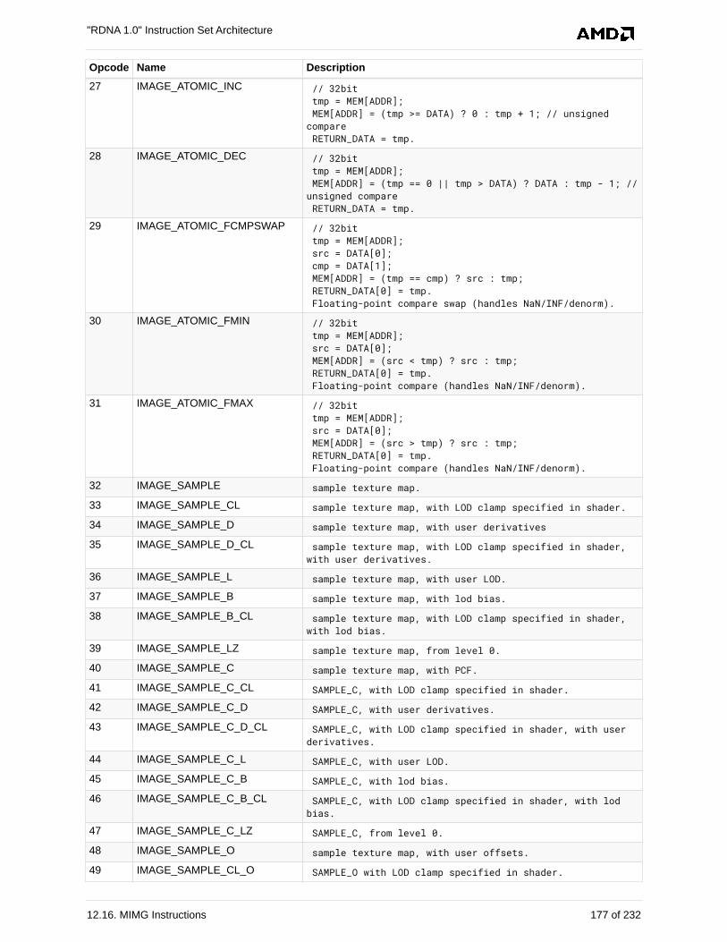
Opcode Name Description
27 IMAGE_ATOMIC_INC // 32bit tmp = MEM[ADDR]; MEM[ADDR] = (tmp >= DATA) ? 0 : tmp + 1; // unsignedcompare RETURN_DATA = tmp.
28 IMAGE_ATOMIC_DEC // 32bit tmp = MEM[ADDR]; MEM[ADDR] = (tmp == 0 || tmp > DATA) ? DATA : tmp - 1; //unsigned compare RETURN_DATA = tmp.
29 IMAGE_ATOMIC_FCMPSWAP // 32bit tmp = MEM[ADDR]; src = DATA[0]; cmp = DATA[1]; MEM[ADDR] = (tmp == cmp) ? src : tmp; RETURN_DATA[0] = tmp. Floating-point compare swap (handles NaN/INF/denorm).
30 IMAGE_ATOMIC_FMIN // 32bit tmp = MEM[ADDR]; src = DATA[0]; MEM[ADDR] = (src < tmp) ? src : tmp; RETURN_DATA[0] = tmp. Floating-point compare (handles NaN/INF/denorm).
31 IMAGE_ATOMIC_FMAX // 32bit tmp = MEM[ADDR]; src = DATA[0]; MEM[ADDR] = (src > tmp) ? src : tmp; RETURN_DATA[0] = tmp. Floating-point compare (handles NaN/INF/denorm).
32 IMAGE_SAMPLE sample texture map.
33 IMAGE_SAMPLE_CL sample texture map, with LOD clamp specified in shader.
34 IMAGE_SAMPLE_D sample texture map, with user derivatives
35 IMAGE_SAMPLE_D_CL sample texture map, with LOD clamp specified in shader,with user derivatives.
36 IMAGE_SAMPLE_L sample texture map, with user LOD.
37 IMAGE_SAMPLE_B sample texture map, with lod bias.
38 IMAGE_SAMPLE_B_CL sample texture map, with LOD clamp specified in shader,with lod bias.
39 IMAGE_SAMPLE_LZ sample texture map, from level 0.
40 IMAGE_SAMPLE_C sample texture map, with PCF.
41 IMAGE_SAMPLE_C_CL SAMPLE_C, with LOD clamp specified in shader.
42 IMAGE_SAMPLE_C_D SAMPLE_C, with user derivatives.
43 IMAGE_SAMPLE_C_D_CL SAMPLE_C, with LOD clamp specified in shader, with userderivatives.
44 IMAGE_SAMPLE_C_L SAMPLE_C, with user LOD.
45 IMAGE_SAMPLE_C_B SAMPLE_C, with lod bias.
46 IMAGE_SAMPLE_C_B_CL SAMPLE_C, with LOD clamp specified in shader, with lodbias.
47 IMAGE_SAMPLE_C_LZ SAMPLE_C, from level 0.
48 IMAGE_SAMPLE_O sample texture map, with user offsets.
49 IMAGE_SAMPLE_CL_O SAMPLE_O with LOD clamp specified in shader.
"RDNA 1.0" Instruction Set Architecture
12.16. MIMG Instructions 177 of 232
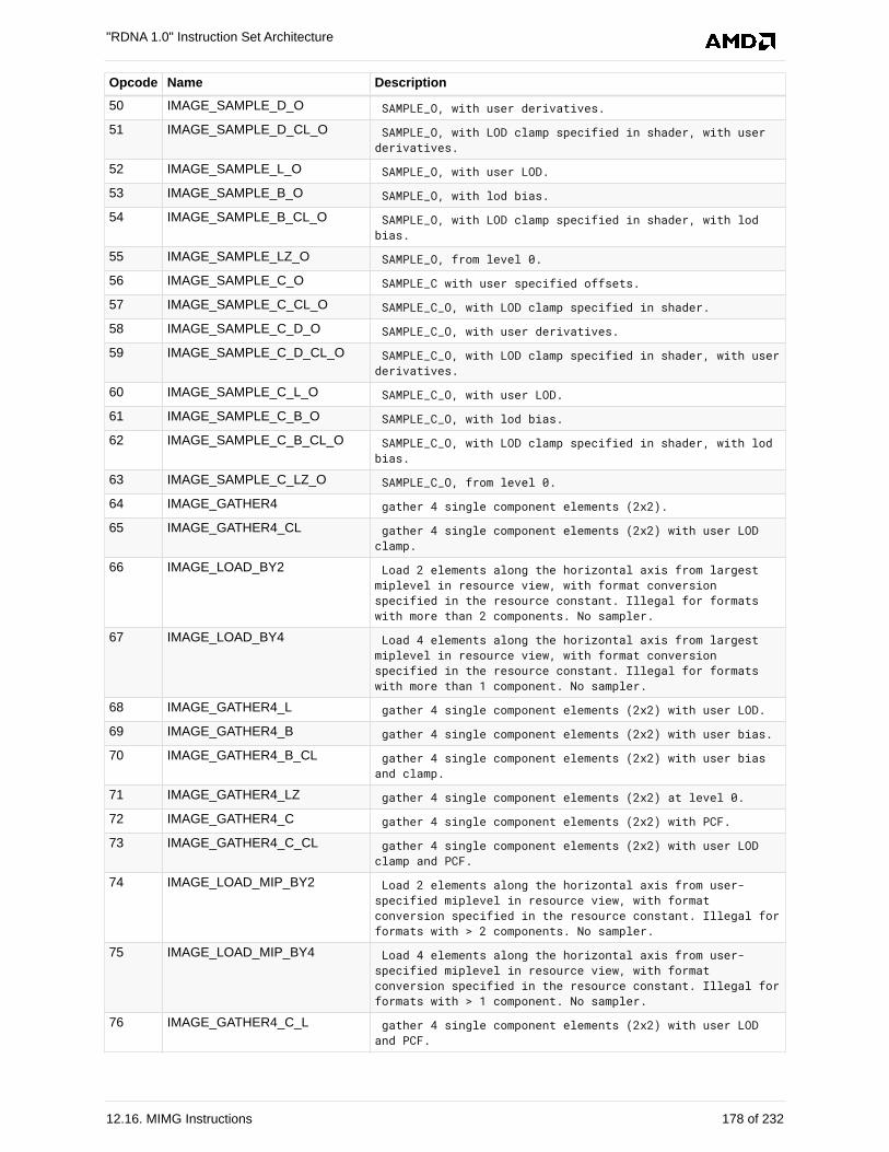
Opcode Name Description
50 IMAGE_SAMPLE_D_O SAMPLE_O, with user derivatives.
51 IMAGE_SAMPLE_D_CL_O SAMPLE_O, with LOD clamp specified in shader, with userderivatives.
52 IMAGE_SAMPLE_L_O SAMPLE_O, with user LOD.
53 IMAGE_SAMPLE_B_O SAMPLE_O, with lod bias.
54 IMAGE_SAMPLE_B_CL_O SAMPLE_O, with LOD clamp specified in shader, with lodbias.
55 IMAGE_SAMPLE_LZ_O SAMPLE_O, from level 0.
56 IMAGE_SAMPLE_C_O SAMPLE_C with user specified offsets.
57 IMAGE_SAMPLE_C_CL_O SAMPLE_C_O, with LOD clamp specified in shader.
58 IMAGE_SAMPLE_C_D_O SAMPLE_C_O, with user derivatives.
59 IMAGE_SAMPLE_C_D_CL_O SAMPLE_C_O, with LOD clamp specified in shader, with userderivatives.
60 IMAGE_SAMPLE_C_L_O SAMPLE_C_O, with user LOD.
61 IMAGE_SAMPLE_C_B_O SAMPLE_C_O, with lod bias.
62 IMAGE_SAMPLE_C_B_CL_O SAMPLE_C_O, with LOD clamp specified in shader, with lodbias.
63 IMAGE_SAMPLE_C_LZ_O SAMPLE_C_O, from level 0.
64 IMAGE_GATHER4 gather 4 single component elements (2x2).
65 IMAGE_GATHER4_CL gather 4 single component elements (2x2) with user LODclamp.
66 IMAGE_LOAD_BY2 Load 2 elements along the horizontal axis from largestmiplevel in resource view, with format conversionspecified in the resource constant. Illegal for formatswith more than 2 components. No sampler.
67 IMAGE_LOAD_BY4 Load 4 elements along the horizontal axis from largestmiplevel in resource view, with format conversionspecified in the resource constant. Illegal for formatswith more than 1 component. No sampler.
68 IMAGE_GATHER4_L gather 4 single component elements (2x2) with user LOD.
69 IMAGE_GATHER4_B gather 4 single component elements (2x2) with user bias.
70 IMAGE_GATHER4_B_CL gather 4 single component elements (2x2) with user biasand clamp.
71 IMAGE_GATHER4_LZ gather 4 single component elements (2x2) at level 0.
72 IMAGE_GATHER4_C gather 4 single component elements (2x2) with PCF.
73 IMAGE_GATHER4_C_CL gather 4 single component elements (2x2) with user LODclamp and PCF.
74 IMAGE_LOAD_MIP_BY2 Load 2 elements along the horizontal axis from user-specified miplevel in resource view, with formatconversion specified in the resource constant. Illegal forformats with > 2 components. No sampler.
75 IMAGE_LOAD_MIP_BY4 Load 4 elements along the horizontal axis from user-specified miplevel in resource view, with formatconversion specified in the resource constant. Illegal forformats with > 1 component. No sampler.
76 IMAGE_GATHER4_C_L gather 4 single component elements (2x2) with user LODand PCF.
"RDNA 1.0" Instruction Set Architecture
12.16. MIMG Instructions 178 of 232
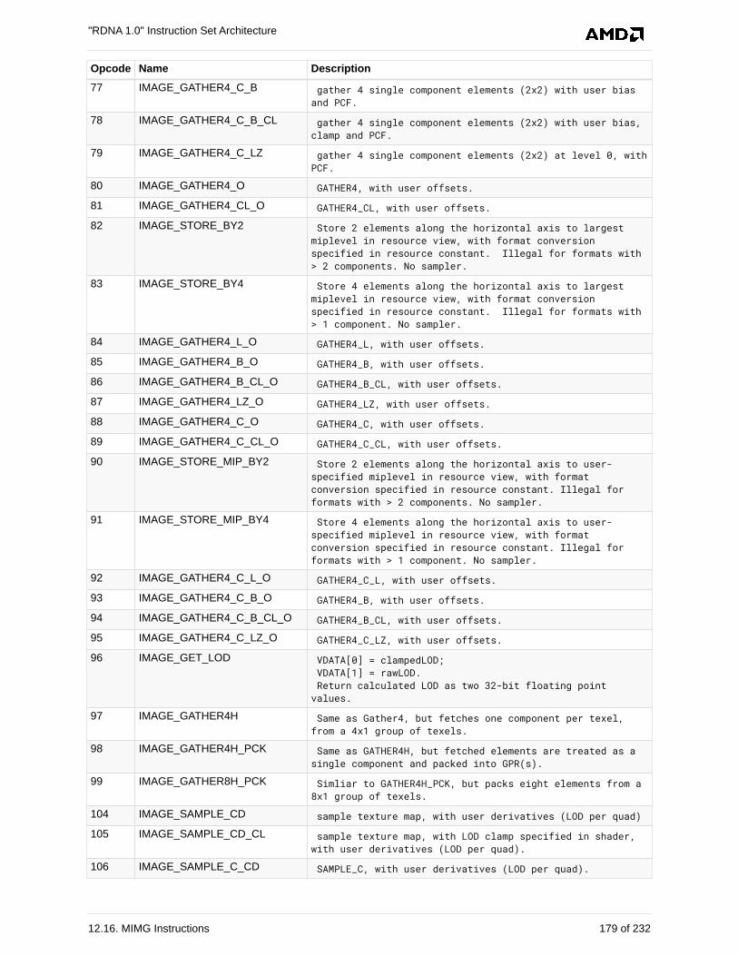
Opcode Name Description
77 IMAGE_GATHER4_C_B gather 4 single component elements (2x2) with user biasand PCF.
78 IMAGE_GATHER4_C_B_CL gather 4 single component elements (2x2) with user bias,clamp and PCF.
79 IMAGE_GATHER4_C_LZ gather 4 single component elements (2x2) at level 0, withPCF.
80 IMAGE_GATHER4_O GATHER4, with user offsets.
81 IMAGE_GATHER4_CL_O GATHER4_CL, with user offsets.
82 IMAGE_STORE_BY2 Store 2 elements along the horizontal axis to largestmiplevel in resource view, with format conversionspecified in resource constant. Illegal for formats with> 2 components. No sampler.
83 IMAGE_STORE_BY4 Store 4 elements along the horizontal axis to largestmiplevel in resource view, with format conversionspecified in resource constant. Illegal for formats with> 1 component. No sampler.
84 IMAGE_GATHER4_L_O GATHER4_L, with user offsets.
85 IMAGE_GATHER4_B_O GATHER4_B, with user offsets.
86 IMAGE_GATHER4_B_CL_O GATHER4_B_CL, with user offsets.
87 IMAGE_GATHER4_LZ_O GATHER4_LZ, with user offsets.
88 IMAGE_GATHER4_C_O GATHER4_C, with user offsets.
89 IMAGE_GATHER4_C_CL_O GATHER4_C_CL, with user offsets.
90 IMAGE_STORE_MIP_BY2 Store 2 elements along the horizontal axis to user-specified miplevel in resource view, with formatconversion specified in resource constant. Illegal forformats with > 2 components. No sampler.
91 IMAGE_STORE_MIP_BY4 Store 4 elements along the horizontal axis to user-specified miplevel in resource view, with formatconversion specified in resource constant. Illegal forformats with > 1 component. No sampler.
92 IMAGE_GATHER4_C_L_O GATHER4_C_L, with user offsets.
93 IMAGE_GATHER4_C_B_O GATHER4_B, with user offsets.
94 IMAGE_GATHER4_C_B_CL_O GATHER4_B_CL, with user offsets.
95 IMAGE_GATHER4_C_LZ_O GATHER4_C_LZ, with user offsets.
96 IMAGE_GET_LOD VDATA[0] = clampedLOD; VDATA[1] = rawLOD. Return calculated LOD as two 32-bit floating pointvalues.
97 IMAGE_GATHER4H Same as Gather4, but fetches one component per texel,from a 4x1 group of texels.
98 IMAGE_GATHER4H_PCK Same as GATHER4H, but fetched elements are treated as asingle component and packed into GPR(s).
99 IMAGE_GATHER8H_PCK Simliar to GATHER4H_PCK, but packs eight elements from a8x1 group of texels.
104 IMAGE_SAMPLE_CD sample texture map, with user derivatives (LOD per quad)
105 IMAGE_SAMPLE_CD_CL sample texture map, with LOD clamp specified in shader,with user derivatives (LOD per quad).
106 IMAGE_SAMPLE_C_CD SAMPLE_C, with user derivatives (LOD per quad).
"RDNA 1.0" Instruction Set Architecture
12.16. MIMG Instructions 179 of 232
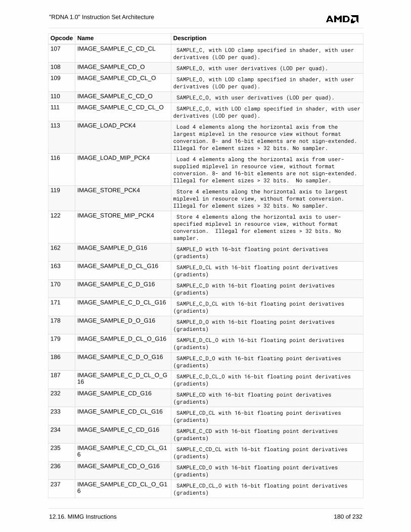
Opcode Name Description
107 IMAGE_SAMPLE_C_CD_CL SAMPLE_C, with LOD clamp specified in shader, with userderivatives (LOD per quad).
108 IMAGE_SAMPLE_CD_O SAMPLE_O, with user derivatives (LOD per quad).
109 IMAGE_SAMPLE_CD_CL_O SAMPLE_O, with LOD clamp specified in shader, with userderivatives (LOD per quad).
110 IMAGE_SAMPLE_C_CD_O SAMPLE_C_O, with user derivatives (LOD per quad).
111 IMAGE_SAMPLE_C_CD_CL_O SAMPLE_C_O, with LOD clamp specified in shader, with userderivatives (LOD per quad).
113 IMAGE_LOAD_PCK4 Load 4 elements along the horizontal axis from thelargest miplevel in the resource view without formatconversion. 8- and 16-bit elements are not sign-extended.Illegal for element sizes > 32 bits. No sampler.
116 IMAGE_LOAD_MIP_PCK4 Load 4 elements along the horizontal axis from user-supplied miplevel in resource view, without formatconversion. 8- and 16-bit elements are not sign-extended.Illegal for element sizes > 32 bits. No sampler.
119 IMAGE_STORE_PCK4 Store 4 elements along the horizontal axis to largestmiplevel in resource view, without format conversion.Illegal for element sizes > 32 bits. No sampler.
122 IMAGE_STORE_MIP_PCK4 Store 4 elements along the horizontal axis to user-specified miplevel in resource view, without formatconversion. Illegal for element sizes > 32 bits. Nosampler.
162 IMAGE_SAMPLE_D_G16 SAMPLE_D with 16-bit floating point derivatives(gradients)
163 IMAGE_SAMPLE_D_CL_G16 SAMPLE_D_CL with 16-bit floating point derivatives(gradients)
170 IMAGE_SAMPLE_C_D_G16 SAMPLE_C_D with 16-bit floating point derivatives(gradients)
171 IMAGE_SAMPLE_C_D_CL_G16 SAMPLE_C_D_CL with 16-bit floating point derivatives(gradients)
178 IMAGE_SAMPLE_D_O_G16 SAMPLE_D_O with 16-bit floating point derivatives(gradients)
179 IMAGE_SAMPLE_D_CL_O_G16 SAMPLE_D_CL_O with 16-bit floating point derivatives(gradients)
186 IMAGE_SAMPLE_C_D_O_G16 SAMPLE_C_D_O with 16-bit floating point derivatives(gradients)
187 IMAGE_SAMPLE_C_D_CL_O_G16
SAMPLE_C_D_CL_O with 16-bit floating point derivatives(gradients)
232 IMAGE_SAMPLE_CD_G16 SAMPLE_CD with 16-bit floating point derivatives(gradients)
233 IMAGE_SAMPLE_CD_CL_G16 SAMPLE_CD_CL with 16-bit floating point derivatives(gradients)
234 IMAGE_SAMPLE_C_CD_G16 SAMPLE_C_CD with 16-bit floating point derivatives(gradients)
235 IMAGE_SAMPLE_C_CD_CL_G16
SAMPLE_C_CD_CL with 16-bit floating point derivatives(gradients)
236 IMAGE_SAMPLE_CD_O_G16 SAMPLE_CD_O with 16-bit floating point derivatives(gradients)
237 IMAGE_SAMPLE_CD_CL_O_G16
SAMPLE_CD_CL_O with 16-bit floating point derivatives(gradients)
"RDNA 1.0" Instruction Set Architecture
12.16. MIMG Instructions 180 of 232
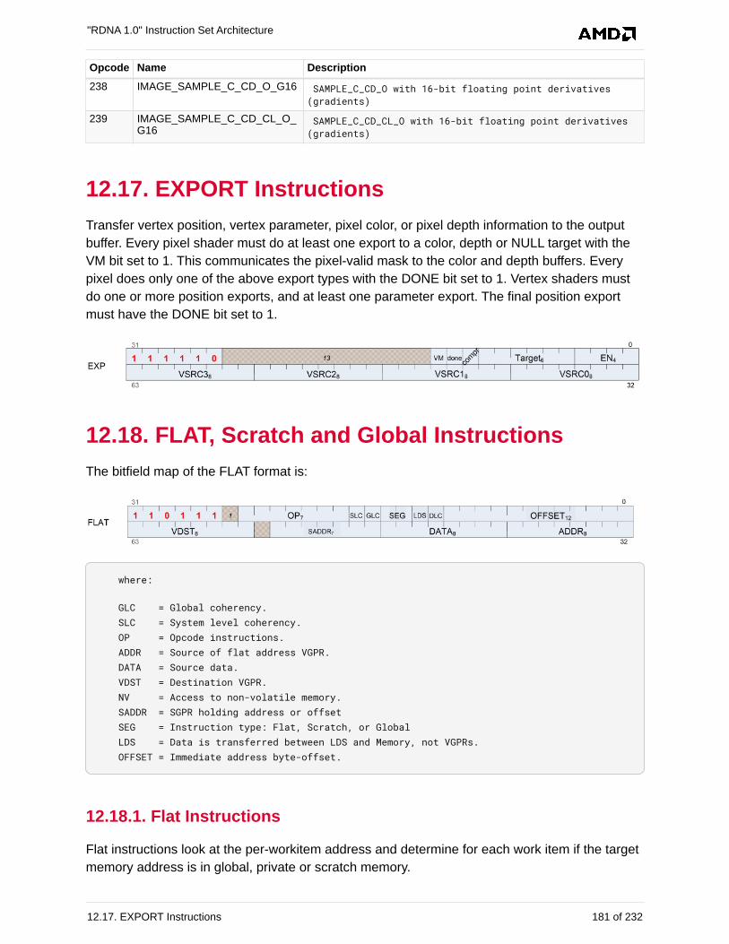
Opcode Name Description
238 IMAGE_SAMPLE_C_CD_O_G16 SAMPLE_C_CD_O with 16-bit floating point derivatives(gradients)
239 IMAGE_SAMPLE_C_CD_CL_O_G16
SAMPLE_C_CD_CL_O with 16-bit floating point derivatives(gradients)
12.17. EXPORT Instructions
Transfer vertex position, vertex parameter, pixel color, or pixel depth information to the output
buffer. Every pixel shader must do at least one export to a color, depth or NULL target with the
VM bit set to 1. This communicates the pixel-valid mask to the color and depth buffers. Every
pixel does only one of the above export types with the DONE bit set to 1. Vertex shaders must
do one or more position exports, and at least one parameter export. The final position export
must have the DONE bit set to 1.
12.18. FLAT, Scratch and Global Instructions
The bitfield map of the FLAT format is:
where:
GLC = Global coherency. SLC = System level coherency. OP = Opcode instructions. ADDR = Source of flat address VGPR. DATA = Source data. VDST = Destination VGPR. NV = Access to non-volatile memory. SADDR = SGPR holding address or offset SEG = Instruction type: Flat, Scratch, or Global LDS = Data is transferred between LDS and Memory, not VGPRs. OFFSET = Immediate address byte-offset.
12.18.1. Flat Instructions
Flat instructions look at the per-workitem address and determine for each work item if the target
memory address is in global, private or scratch memory.
"RDNA 1.0" Instruction Set Architecture
12.17. EXPORT Instructions 181 of 232
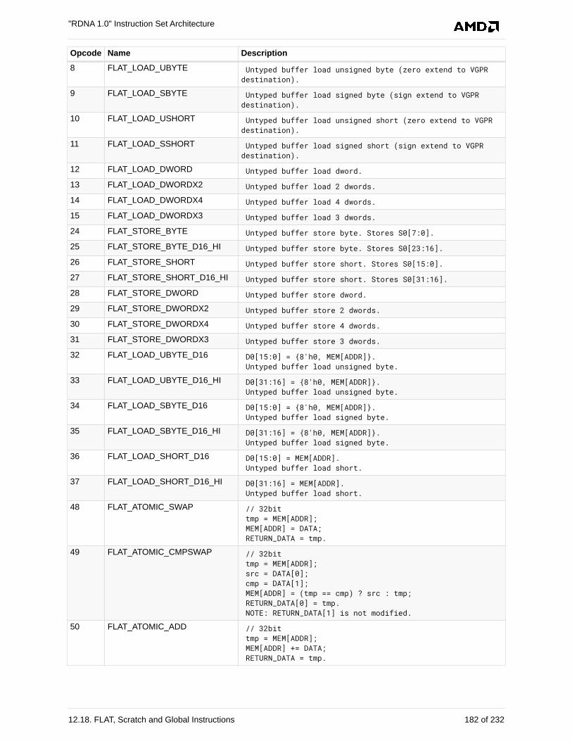
Opcode Name Description
8 FLAT_LOAD_UBYTE Untyped buffer load unsigned byte (zero extend to VGPRdestination).
9 FLAT_LOAD_SBYTE Untyped buffer load signed byte (sign extend to VGPRdestination).
10 FLAT_LOAD_USHORT Untyped buffer load unsigned short (zero extend to VGPRdestination).
11 FLAT_LOAD_SSHORT Untyped buffer load signed short (sign extend to VGPRdestination).
12 FLAT_LOAD_DWORD Untyped buffer load dword.
13 FLAT_LOAD_DWORDX2 Untyped buffer load 2 dwords.
14 FLAT_LOAD_DWORDX4 Untyped buffer load 4 dwords.
15 FLAT_LOAD_DWORDX3 Untyped buffer load 3 dwords.
24 FLAT_STORE_BYTE Untyped buffer store byte. Stores S0[7:0].
25 FLAT_STORE_BYTE_D16_HI Untyped buffer store byte. Stores S0[23:16].
26 FLAT_STORE_SHORT Untyped buffer store short. Stores S0[15:0].
27 FLAT_STORE_SHORT_D16_HI Untyped buffer store short. Stores S0[31:16].
28 FLAT_STORE_DWORD Untyped buffer store dword.
29 FLAT_STORE_DWORDX2 Untyped buffer store 2 dwords.
30 FLAT_STORE_DWORDX4 Untyped buffer store 4 dwords.
31 FLAT_STORE_DWORDX3 Untyped buffer store 3 dwords.
32 FLAT_LOAD_UBYTE_D16 D0[15:0] = {8'h0, MEM[ADDR]}. Untyped buffer load unsigned byte.
33 FLAT_LOAD_UBYTE_D16_HI D0[31:16] = {8'h0, MEM[ADDR]}. Untyped buffer load unsigned byte.
34 FLAT_LOAD_SBYTE_D16 D0[15:0] = {8'h0, MEM[ADDR]}. Untyped buffer load signed byte.
35 FLAT_LOAD_SBYTE_D16_HI D0[31:16] = {8'h0, MEM[ADDR]}. Untyped buffer load signed byte.
36 FLAT_LOAD_SHORT_D16 D0[15:0] = MEM[ADDR]. Untyped buffer load short.
37 FLAT_LOAD_SHORT_D16_HI D0[31:16] = MEM[ADDR]. Untyped buffer load short.
48 FLAT_ATOMIC_SWAP // 32bit tmp = MEM[ADDR]; MEM[ADDR] = DATA; RETURN_DATA = tmp.
49 FLAT_ATOMIC_CMPSWAP // 32bit tmp = MEM[ADDR]; src = DATA[0]; cmp = DATA[1]; MEM[ADDR] = (tmp == cmp) ? src : tmp; RETURN_DATA[0] = tmp. NOTE: RETURN_DATA[1] is not modified.
50 FLAT_ATOMIC_ADD // 32bit tmp = MEM[ADDR]; MEM[ADDR] += DATA; RETURN_DATA = tmp.
"RDNA 1.0" Instruction Set Architecture
12.18. FLAT, Scratch and Global Instructions 182 of 232
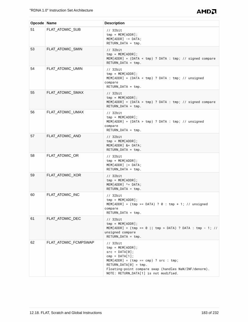
Opcode Name Description
51 FLAT_ATOMIC_SUB // 32bit tmp = MEM[ADDR]; MEM[ADDR] -= DATA; RETURN_DATA = tmp.
53 FLAT_ATOMIC_SMIN // 32bit tmp = MEM[ADDR]; MEM[ADDR] = (DATA < tmp) ? DATA : tmp; // signed compare RETURN_DATA = tmp.
54 FLAT_ATOMIC_UMIN // 32bit tmp = MEM[ADDR]; MEM[ADDR] = (DATA < tmp) ? DATA : tmp; // unsignedcompare RETURN_DATA = tmp.
55 FLAT_ATOMIC_SMAX // 32bit tmp = MEM[ADDR]; MEM[ADDR] = (DATA > tmp) ? DATA : tmp; // signed compare RETURN_DATA = tmp.
56 FLAT_ATOMIC_UMAX // 32bit tmp = MEM[ADDR]; MEM[ADDR] = (DATA > tmp) ? DATA : tmp; // unsignedcompare RETURN_DATA = tmp.
57 FLAT_ATOMIC_AND // 32bit tmp = MEM[ADDR]; MEM[ADDR] &= DATA; RETURN_DATA = tmp.
58 FLAT_ATOMIC_OR // 32bit tmp = MEM[ADDR]; MEM[ADDR] |= DATA; RETURN_DATA = tmp.
59 FLAT_ATOMIC_XOR // 32bit tmp = MEM[ADDR]; MEM[ADDR] ^= DATA; RETURN_DATA = tmp.
60 FLAT_ATOMIC_INC // 32bit tmp = MEM[ADDR]; MEM[ADDR] = (tmp >= DATA) ? 0 : tmp + 1; // unsignedcompare RETURN_DATA = tmp.
61 FLAT_ATOMIC_DEC // 32bit tmp = MEM[ADDR]; MEM[ADDR] = (tmp == 0 || tmp > DATA) ? DATA : tmp - 1; //unsigned compare RETURN_DATA = tmp.
62 FLAT_ATOMIC_FCMPSWAP // 32bit tmp = MEM[ADDR]; src = DATA[0]; cmp = DATA[1]; MEM[ADDR] = (tmp == cmp) ? src : tmp; RETURN_DATA[0] = tmp. Floating-point compare swap (handles NaN/INF/denorm). NOTE: RETURN_DATA[1] is not modified.
"RDNA 1.0" Instruction Set Architecture
12.18. FLAT, Scratch and Global Instructions 183 of 232
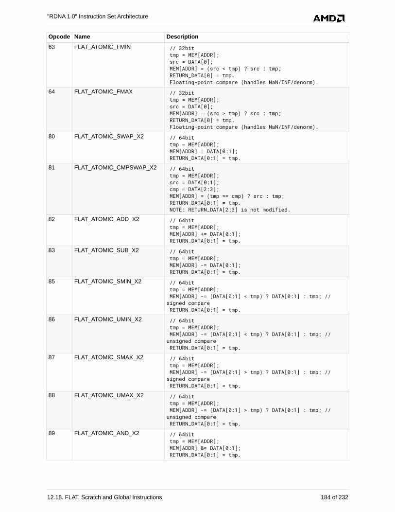
Opcode Name Description
63 FLAT_ATOMIC_FMIN // 32bit tmp = MEM[ADDR]; src = DATA[0]; MEM[ADDR] = (src < tmp) ? src : tmp; RETURN_DATA[0] = tmp. Floating-point compare (handles NaN/INF/denorm).
64 FLAT_ATOMIC_FMAX // 32bit tmp = MEM[ADDR]; src = DATA[0]; MEM[ADDR] = (src > tmp) ? src : tmp; RETURN_DATA[0] = tmp. Floating-point compare (handles NaN/INF/denorm).
80 FLAT_ATOMIC_SWAP_X2 // 64bit tmp = MEM[ADDR]; MEM[ADDR] = DATA[0:1]; RETURN_DATA[0:1] = tmp.
81 FLAT_ATOMIC_CMPSWAP_X2 // 64bit tmp = MEM[ADDR]; src = DATA[0:1]; cmp = DATA[2:3]; MEM[ADDR] = (tmp == cmp) ? src : tmp; RETURN_DATA[0:1] = tmp. NOTE: RETURN_DATA[2:3] is not modified.
82 FLAT_ATOMIC_ADD_X2 // 64bit tmp = MEM[ADDR]; MEM[ADDR] += DATA[0:1]; RETURN_DATA[0:1] = tmp.
83 FLAT_ATOMIC_SUB_X2 // 64bit tmp = MEM[ADDR]; MEM[ADDR] -= DATA[0:1]; RETURN_DATA[0:1] = tmp.
85 FLAT_ATOMIC_SMIN_X2 // 64bit tmp = MEM[ADDR]; MEM[ADDR] -= (DATA[0:1] < tmp) ? DATA[0:1] : tmp; //signed compare RETURN_DATA[0:1] = tmp.
86 FLAT_ATOMIC_UMIN_X2 // 64bit tmp = MEM[ADDR]; MEM[ADDR] -= (DATA[0:1] < tmp) ? DATA[0:1] : tmp; //unsigned compare RETURN_DATA[0:1] = tmp.
87 FLAT_ATOMIC_SMAX_X2 // 64bit tmp = MEM[ADDR]; MEM[ADDR] -= (DATA[0:1] > tmp) ? DATA[0:1] : tmp; //signed compare RETURN_DATA[0:1] = tmp.
88 FLAT_ATOMIC_UMAX_X2 // 64bit tmp = MEM[ADDR]; MEM[ADDR] -= (DATA[0:1] > tmp) ? DATA[0:1] : tmp; //unsigned compare RETURN_DATA[0:1] = tmp.
89 FLAT_ATOMIC_AND_X2 // 64bit tmp = MEM[ADDR]; MEM[ADDR] &= DATA[0:1]; RETURN_DATA[0:1] = tmp.
"RDNA 1.0" Instruction Set Architecture
12.18. FLAT, Scratch and Global Instructions 184 of 232
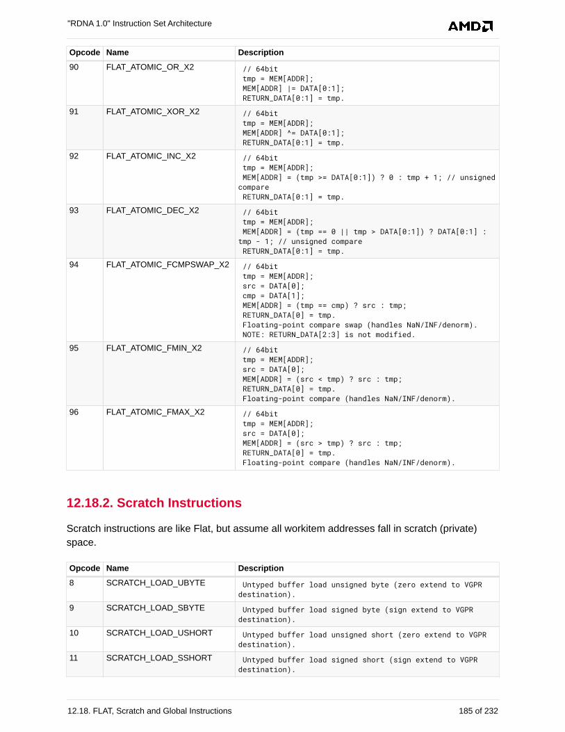
Opcode Name Description
90 FLAT_ATOMIC_OR_X2 // 64bit tmp = MEM[ADDR]; MEM[ADDR] |= DATA[0:1]; RETURN_DATA[0:1] = tmp.
91 FLAT_ATOMIC_XOR_X2 // 64bit tmp = MEM[ADDR]; MEM[ADDR] ^= DATA[0:1]; RETURN_DATA[0:1] = tmp.
92 FLAT_ATOMIC_INC_X2 // 64bit tmp = MEM[ADDR]; MEM[ADDR] = (tmp >= DATA[0:1]) ? 0 : tmp + 1; // unsignedcompare RETURN_DATA[0:1] = tmp.
93 FLAT_ATOMIC_DEC_X2 // 64bit tmp = MEM[ADDR]; MEM[ADDR] = (tmp == 0 || tmp > DATA[0:1]) ? DATA[0:1] :tmp - 1; // unsigned compare RETURN_DATA[0:1] = tmp.
94 FLAT_ATOMIC_FCMPSWAP_X2 // 64bit tmp = MEM[ADDR]; src = DATA[0]; cmp = DATA[1]; MEM[ADDR] = (tmp == cmp) ? src : tmp; RETURN_DATA[0] = tmp. Floating-point compare swap (handles NaN/INF/denorm). NOTE: RETURN_DATA[2:3] is not modified.
95 FLAT_ATOMIC_FMIN_X2 // 64bit tmp = MEM[ADDR]; src = DATA[0]; MEM[ADDR] = (src < tmp) ? src : tmp; RETURN_DATA[0] = tmp. Floating-point compare (handles NaN/INF/denorm).
96 FLAT_ATOMIC_FMAX_X2 // 64bit tmp = MEM[ADDR]; src = DATA[0]; MEM[ADDR] = (src > tmp) ? src : tmp; RETURN_DATA[0] = tmp. Floating-point compare (handles NaN/INF/denorm).
12.18.2. Scratch Instructions
Scratch instructions are like Flat, but assume all workitem addresses fall in scratch (private)
space.
Opcode Name Description
8 SCRATCH_LOAD_UBYTE Untyped buffer load unsigned byte (zero extend to VGPRdestination).
9 SCRATCH_LOAD_SBYTE Untyped buffer load signed byte (sign extend to VGPRdestination).
10 SCRATCH_LOAD_USHORT Untyped buffer load unsigned short (zero extend to VGPRdestination).
11 SCRATCH_LOAD_SSHORT Untyped buffer load signed short (sign extend to VGPRdestination).
"RDNA 1.0" Instruction Set Architecture
12.18. FLAT, Scratch and Global Instructions 185 of 232
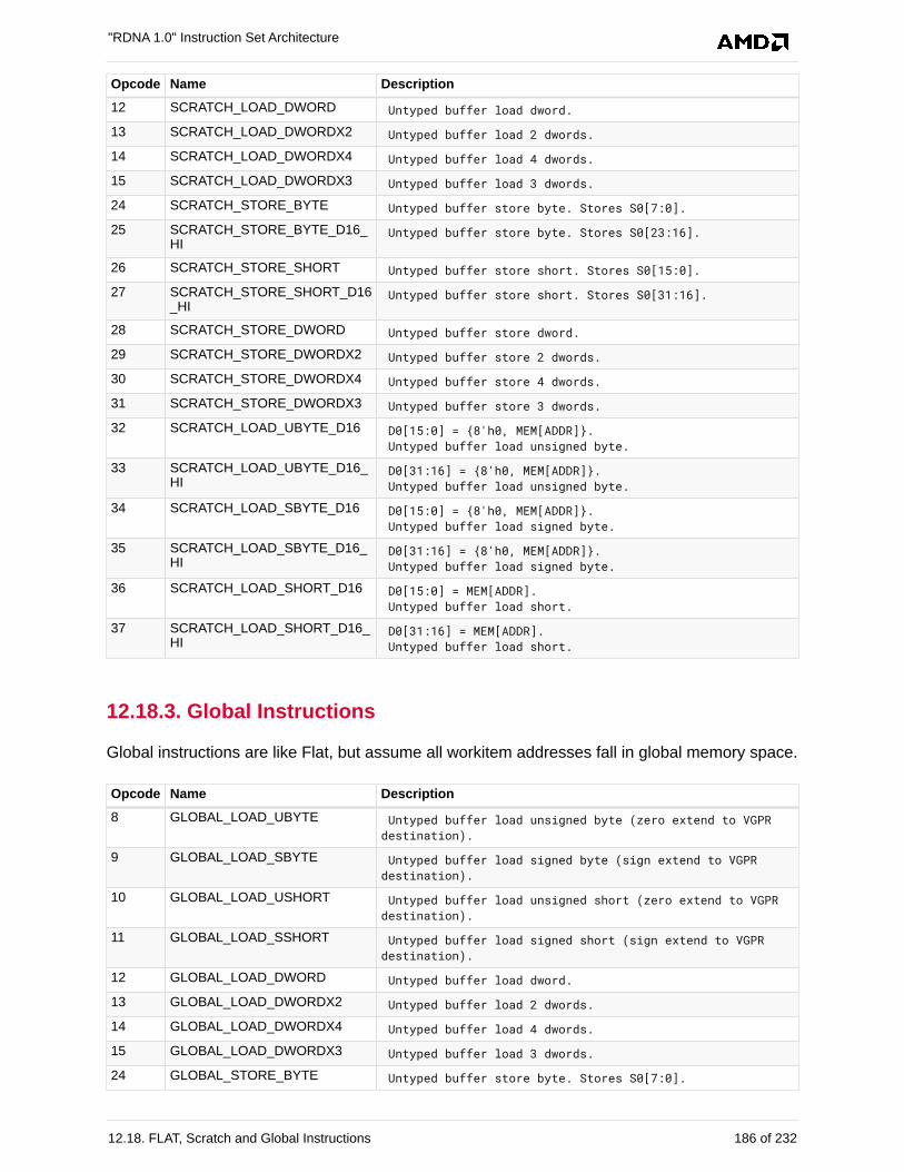
Opcode Name Description
12 SCRATCH_LOAD_DWORD Untyped buffer load dword.
13 SCRATCH_LOAD_DWORDX2 Untyped buffer load 2 dwords.
14 SCRATCH_LOAD_DWORDX4 Untyped buffer load 4 dwords.
15 SCRATCH_LOAD_DWORDX3 Untyped buffer load 3 dwords.
24 SCRATCH_STORE_BYTE Untyped buffer store byte. Stores S0[7:0].
25 SCRATCH_STORE_BYTE_D16_HI
Untyped buffer store byte. Stores S0[23:16].
26 SCRATCH_STORE_SHORT Untyped buffer store short. Stores S0[15:0].
27 SCRATCH_STORE_SHORT_D16_HI
Untyped buffer store short. Stores S0[31:16].
28 SCRATCH_STORE_DWORD Untyped buffer store dword.
29 SCRATCH_STORE_DWORDX2 Untyped buffer store 2 dwords.
30 SCRATCH_STORE_DWORDX4 Untyped buffer store 4 dwords.
31 SCRATCH_STORE_DWORDX3 Untyped buffer store 3 dwords.
32 SCRATCH_LOAD_UBYTE_D16 D0[15:0] = {8'h0, MEM[ADDR]}. Untyped buffer load unsigned byte.
33 SCRATCH_LOAD_UBYTE_D16_HI
D0[31:16] = {8'h0, MEM[ADDR]}. Untyped buffer load unsigned byte.
34 SCRATCH_LOAD_SBYTE_D16 D0[15:0] = {8'h0, MEM[ADDR]}. Untyped buffer load signed byte.
35 SCRATCH_LOAD_SBYTE_D16_HI
D0[31:16] = {8'h0, MEM[ADDR]}. Untyped buffer load signed byte.
36 SCRATCH_LOAD_SHORT_D16 D0[15:0] = MEM[ADDR]. Untyped buffer load short.
37 SCRATCH_LOAD_SHORT_D16_HI
D0[31:16] = MEM[ADDR]. Untyped buffer load short.
12.18.3. Global Instructions
Global instructions are like Flat, but assume all workitem addresses fall in global memory space.
Opcode Name Description
8 GLOBAL_LOAD_UBYTE Untyped buffer load unsigned byte (zero extend to VGPRdestination).
9 GLOBAL_LOAD_SBYTE Untyped buffer load signed byte (sign extend to VGPRdestination).
10 GLOBAL_LOAD_USHORT Untyped buffer load unsigned short (zero extend to VGPRdestination).
11 GLOBAL_LOAD_SSHORT Untyped buffer load signed short (sign extend to VGPRdestination).
12 GLOBAL_LOAD_DWORD Untyped buffer load dword.
13 GLOBAL_LOAD_DWORDX2 Untyped buffer load 2 dwords.
14 GLOBAL_LOAD_DWORDX4 Untyped buffer load 4 dwords.
15 GLOBAL_LOAD_DWORDX3 Untyped buffer load 3 dwords.
24 GLOBAL_STORE_BYTE Untyped buffer store byte. Stores S0[7:0].
"RDNA 1.0" Instruction Set Architecture
12.18. FLAT, Scratch and Global Instructions 186 of 232
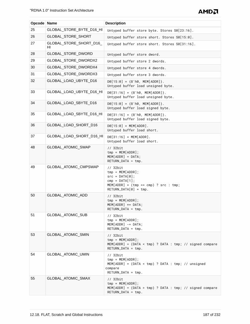
Opcode Name Description
25 GLOBAL_STORE_BYTE_D16_HI Untyped buffer store byte. Stores S0[23:16].
26 GLOBAL_STORE_SHORT Untyped buffer store short. Stores S0[15:0].
27 GLOBAL_STORE_SHORT_D16_HI
Untyped buffer store short. Stores S0[31:16].
28 GLOBAL_STORE_DWORD Untyped buffer store dword.
29 GLOBAL_STORE_DWORDX2 Untyped buffer store 2 dwords.
30 GLOBAL_STORE_DWORDX4 Untyped buffer store 4 dwords.
31 GLOBAL_STORE_DWORDX3 Untyped buffer store 3 dwords.
32 GLOBAL_LOAD_UBYTE_D16 D0[15:0] = {8'h0, MEM[ADDR]}. Untyped buffer load unsigned byte.
33 GLOBAL_LOAD_UBYTE_D16_HI D0[31:16] = {8'h0, MEM[ADDR]}. Untyped buffer load unsigned byte.
34 GLOBAL_LOAD_SBYTE_D16 D0[15:0] = {8'h0, MEM[ADDR]}. Untyped buffer load signed byte.
35 GLOBAL_LOAD_SBYTE_D16_HI D0[31:16] = {8'h0, MEM[ADDR]}. Untyped buffer load signed byte.
36 GLOBAL_LOAD_SHORT_D16 D0[15:0] = MEM[ADDR]. Untyped buffer load short.
37 GLOBAL_LOAD_SHORT_D16_HI D0[31:16] = MEM[ADDR]. Untyped buffer load short.
48 GLOBAL_ATOMIC_SWAP // 32bit tmp = MEM[ADDR]; MEM[ADDR] = DATA; RETURN_DATA = tmp.
49 GLOBAL_ATOMIC_CMPSWAP // 32bit tmp = MEM[ADDR]; src = DATA[0]; cmp = DATA[1]; MEM[ADDR] = (tmp == cmp) ? src : tmp; RETURN_DATA[0] = tmp.
50 GLOBAL_ATOMIC_ADD // 32bit tmp = MEM[ADDR]; MEM[ADDR] += DATA; RETURN_DATA = tmp.
51 GLOBAL_ATOMIC_SUB // 32bit tmp = MEM[ADDR]; MEM[ADDR] -= DATA; RETURN_DATA = tmp.
53 GLOBAL_ATOMIC_SMIN // 32bit tmp = MEM[ADDR]; MEM[ADDR] = (DATA < tmp) ? DATA : tmp; // signed compare RETURN_DATA = tmp.
54 GLOBAL_ATOMIC_UMIN // 32bit tmp = MEM[ADDR]; MEM[ADDR] = (DATA < tmp) ? DATA : tmp; // unsignedcompare RETURN_DATA = tmp.
55 GLOBAL_ATOMIC_SMAX // 32bit tmp = MEM[ADDR]; MEM[ADDR] = (DATA > tmp) ? DATA : tmp; // signed compare RETURN_DATA = tmp.
"RDNA 1.0" Instruction Set Architecture
12.18. FLAT, Scratch and Global Instructions 187 of 232
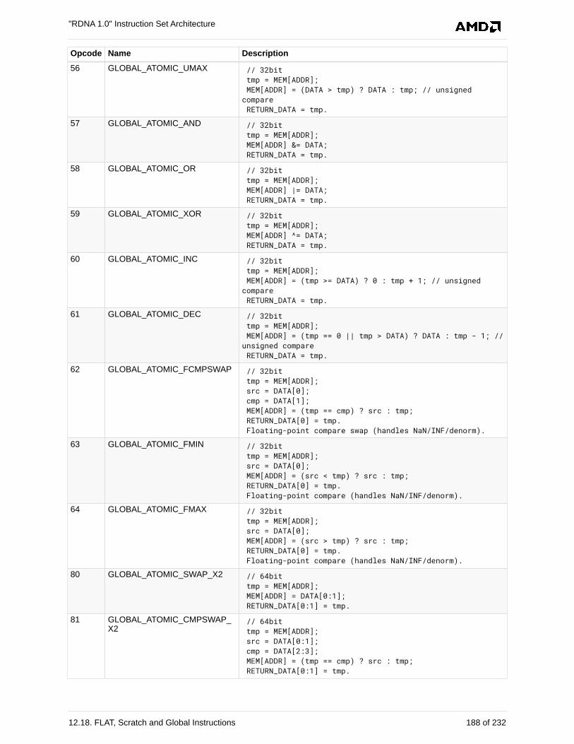
Opcode Name Description
56 GLOBAL_ATOMIC_UMAX // 32bit tmp = MEM[ADDR]; MEM[ADDR] = (DATA > tmp) ? DATA : tmp; // unsignedcompare RETURN_DATA = tmp.
57 GLOBAL_ATOMIC_AND // 32bit tmp = MEM[ADDR]; MEM[ADDR] &= DATA; RETURN_DATA = tmp.
58 GLOBAL_ATOMIC_OR // 32bit tmp = MEM[ADDR]; MEM[ADDR] |= DATA; RETURN_DATA = tmp.
59 GLOBAL_ATOMIC_XOR // 32bit tmp = MEM[ADDR]; MEM[ADDR] ^= DATA; RETURN_DATA = tmp.
60 GLOBAL_ATOMIC_INC // 32bit tmp = MEM[ADDR]; MEM[ADDR] = (tmp >= DATA) ? 0 : tmp + 1; // unsignedcompare RETURN_DATA = tmp.
61 GLOBAL_ATOMIC_DEC // 32bit tmp = MEM[ADDR]; MEM[ADDR] = (tmp == 0 || tmp > DATA) ? DATA : tmp - 1; //unsigned compare RETURN_DATA = tmp.
62 GLOBAL_ATOMIC_FCMPSWAP // 32bit tmp = MEM[ADDR]; src = DATA[0]; cmp = DATA[1]; MEM[ADDR] = (tmp == cmp) ? src : tmp; RETURN_DATA[0] = tmp. Floating-point compare swap (handles NaN/INF/denorm).
63 GLOBAL_ATOMIC_FMIN // 32bit tmp = MEM[ADDR]; src = DATA[0]; MEM[ADDR] = (src < tmp) ? src : tmp; RETURN_DATA[0] = tmp. Floating-point compare (handles NaN/INF/denorm).
64 GLOBAL_ATOMIC_FMAX // 32bit tmp = MEM[ADDR]; src = DATA[0]; MEM[ADDR] = (src > tmp) ? src : tmp; RETURN_DATA[0] = tmp. Floating-point compare (handles NaN/INF/denorm).
80 GLOBAL_ATOMIC_SWAP_X2 // 64bit tmp = MEM[ADDR]; MEM[ADDR] = DATA[0:1]; RETURN_DATA[0:1] = tmp.
81 GLOBAL_ATOMIC_CMPSWAP_X2
// 64bit tmp = MEM[ADDR]; src = DATA[0:1]; cmp = DATA[2:3]; MEM[ADDR] = (tmp == cmp) ? src : tmp; RETURN_DATA[0:1] = tmp.
"RDNA 1.0" Instruction Set Architecture
12.18. FLAT, Scratch and Global Instructions 188 of 232
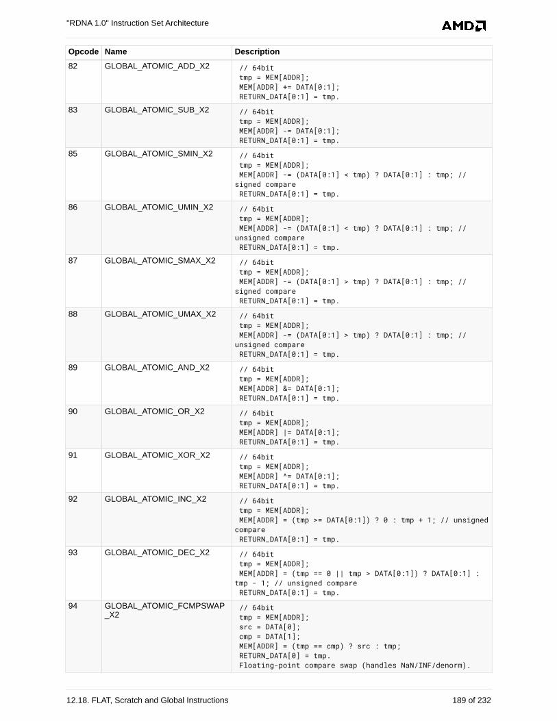
Opcode Name Description
82 GLOBAL_ATOMIC_ADD_X2 // 64bit tmp = MEM[ADDR]; MEM[ADDR] += DATA[0:1]; RETURN_DATA[0:1] = tmp.
83 GLOBAL_ATOMIC_SUB_X2 // 64bit tmp = MEM[ADDR]; MEM[ADDR] -= DATA[0:1]; RETURN_DATA[0:1] = tmp.
85 GLOBAL_ATOMIC_SMIN_X2 // 64bit tmp = MEM[ADDR]; MEM[ADDR] -= (DATA[0:1] < tmp) ? DATA[0:1] : tmp; //signed compare RETURN_DATA[0:1] = tmp.
86 GLOBAL_ATOMIC_UMIN_X2 // 64bit tmp = MEM[ADDR]; MEM[ADDR] -= (DATA[0:1] < tmp) ? DATA[0:1] : tmp; //unsigned compare RETURN_DATA[0:1] = tmp.
87 GLOBAL_ATOMIC_SMAX_X2 // 64bit tmp = MEM[ADDR]; MEM[ADDR] -= (DATA[0:1] > tmp) ? DATA[0:1] : tmp; //signed compare RETURN_DATA[0:1] = tmp.
88 GLOBAL_ATOMIC_UMAX_X2 // 64bit tmp = MEM[ADDR]; MEM[ADDR] -= (DATA[0:1] > tmp) ? DATA[0:1] : tmp; //unsigned compare RETURN_DATA[0:1] = tmp.
89 GLOBAL_ATOMIC_AND_X2 // 64bit tmp = MEM[ADDR]; MEM[ADDR] &= DATA[0:1]; RETURN_DATA[0:1] = tmp.
90 GLOBAL_ATOMIC_OR_X2 // 64bit tmp = MEM[ADDR]; MEM[ADDR] |= DATA[0:1]; RETURN_DATA[0:1] = tmp.
91 GLOBAL_ATOMIC_XOR_X2 // 64bit tmp = MEM[ADDR]; MEM[ADDR] ^= DATA[0:1]; RETURN_DATA[0:1] = tmp.
92 GLOBAL_ATOMIC_INC_X2 // 64bit tmp = MEM[ADDR]; MEM[ADDR] = (tmp >= DATA[0:1]) ? 0 : tmp + 1; // unsignedcompare RETURN_DATA[0:1] = tmp.
93 GLOBAL_ATOMIC_DEC_X2 // 64bit tmp = MEM[ADDR]; MEM[ADDR] = (tmp == 0 || tmp > DATA[0:1]) ? DATA[0:1] :tmp - 1; // unsigned compare RETURN_DATA[0:1] = tmp.
94 GLOBAL_ATOMIC_FCMPSWAP_X2
// 64bit tmp = MEM[ADDR]; src = DATA[0]; cmp = DATA[1]; MEM[ADDR] = (tmp == cmp) ? src : tmp; RETURN_DATA[0] = tmp. Floating-point compare swap (handles NaN/INF/denorm).
"RDNA 1.0" Instruction Set Architecture
12.18. FLAT, Scratch and Global Instructions 189 of 232
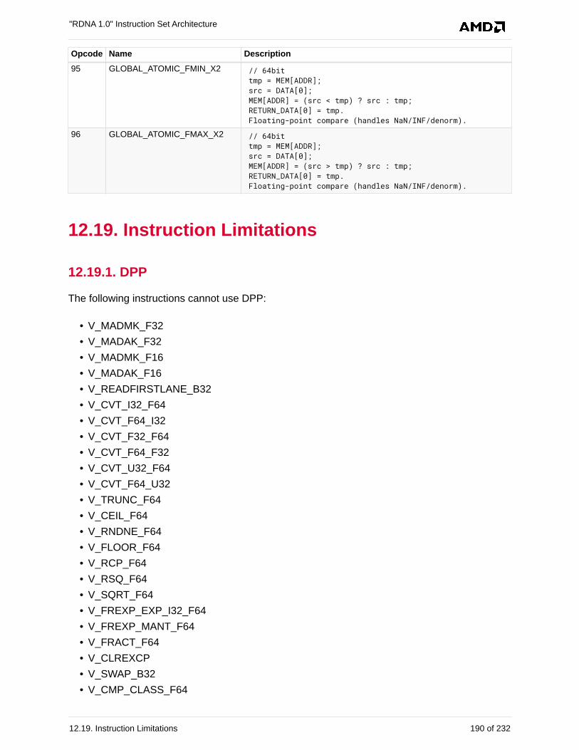
Opcode Name Description
95 GLOBAL_ATOMIC_FMIN_X2 // 64bit tmp = MEM[ADDR]; src = DATA[0]; MEM[ADDR] = (src < tmp) ? src : tmp; RETURN_DATA[0] = tmp. Floating-point compare (handles NaN/INF/denorm).
96 GLOBAL_ATOMIC_FMAX_X2 // 64bit tmp = MEM[ADDR]; src = DATA[0]; MEM[ADDR] = (src > tmp) ? src : tmp; RETURN_DATA[0] = tmp. Floating-point compare (handles NaN/INF/denorm).
12.19. Instruction Limitations
12.19.1. DPP
The following instructions cannot use DPP:
• V_MADMK_F32
• V_MADAK_F32
• V_MADMK_F16
• V_MADAK_F16
• V_READFIRSTLANE_B32
• V_CVT_I32_F64
• V_CVT_F64_I32
• V_CVT_F32_F64
• V_CVT_F64_F32
• V_CVT_U32_F64
• V_CVT_F64_U32
• V_TRUNC_F64
• V_CEIL_F64
• V_RNDNE_F64
• V_FLOOR_F64
• V_RCP_F64
• V_RSQ_F64
• V_SQRT_F64
• V_FREXP_EXP_I32_F64
• V_FREXP_MANT_F64
• V_FRACT_F64
• V_CLREXCP
• V_SWAP_B32
• V_CMP_CLASS_F64
"RDNA 1.0" Instruction Set Architecture
12.19. Instruction Limitations 190 of 232
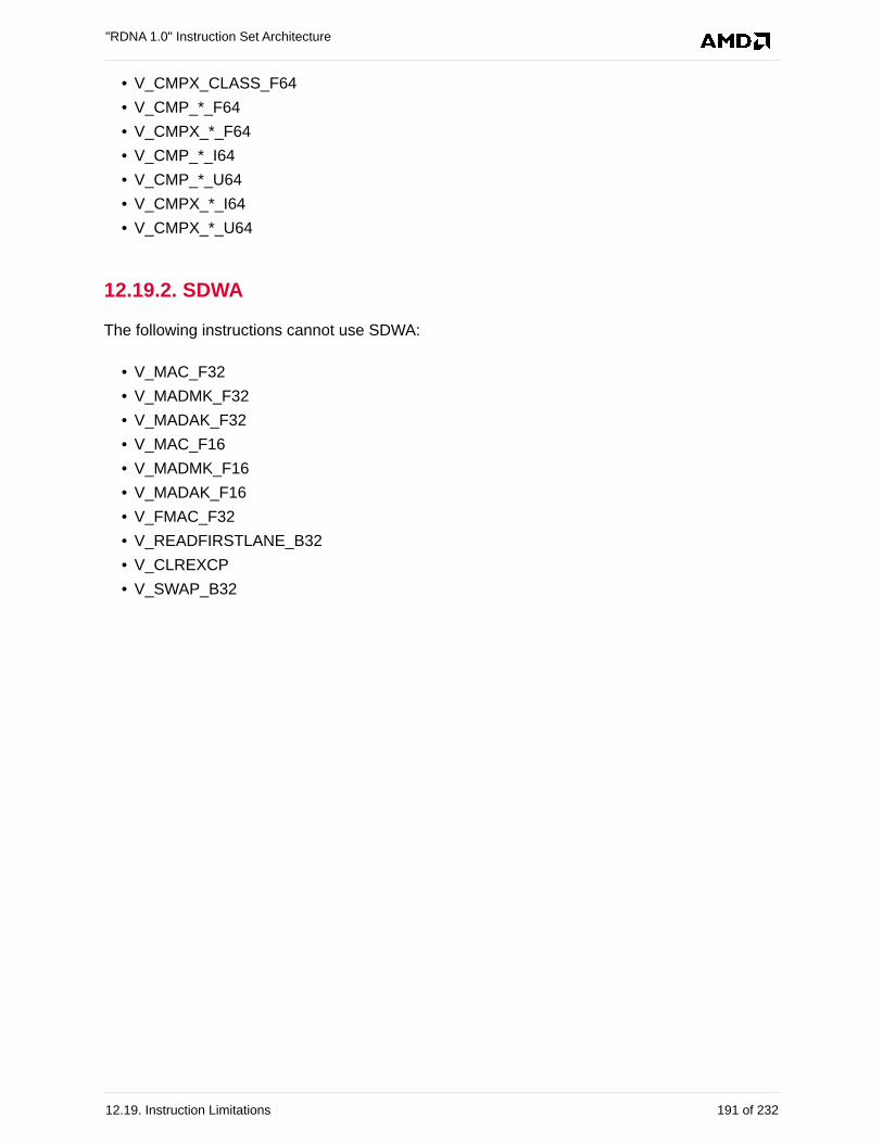
• V_CMPX_CLASS_F64
• V_CMP_*_F64
• V_CMPX_*_F64
• V_CMP_*_I64
• V_CMP_*_U64
• V_CMPX_*_I64
• V_CMPX_*_U64
12.19.2. SDWA
The following instructions cannot use SDWA:
• V_MAC_F32
• V_MADMK_F32
• V_MADAK_F32
• V_MAC_F16
• V_MADMK_F16
• V_MADAK_F16
• V_FMAC_F32
• V_READFIRSTLANE_B32
• V_CLREXCP
• V_SWAP_B32
"RDNA 1.0" Instruction Set Architecture
12.19. Instruction Limitations 191 of 232
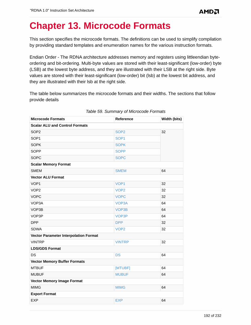
Chapter 13. Microcode Formats
This section specifies the microcode formats. The definitions can be used to simplify compilation
by providing standard templates and enumeration names for the various instruction formats.
Endian Order - The RDNA architecture addresses memory and registers using littleendian byte-
ordering and bit-ordering. Multi-byte values are stored with their least-significant (low-order) byte
(LSB) at the lowest byte address, and they are illustrated with their LSB at the right side. Byte
values are stored with their least-significant (low-order) bit (lsb) at the lowest bit address, and
they are illustrated with their lsb at the right side.
The table below summarizes the microcode formats and their widths. The sections that follow
provide details
Table 59. Summary of Microcode Formats
Microcode Formats Reference Width (bits)
Scalar ALU and Control Formats
SOP2 SOP2 32
SOP1 SOP1
SOPK SOPK
SOPP SOPP
SOPC SOPC
Scalar Memory Format
SMEM SMEM 64
Vector ALU Format
VOP1 VOP1 32
VOP2 VOP2 32
VOPC VOPC 32
VOP3A VOP3A 64
VOP3B VOP3B 64
VOP3P VOP3P 64
DPP DPP 32
SDWA VOP2 32
Vector Parameter Interpolation Format
VINTRP VINTRP 32
LDS/GDS Format
DS DS 64
Vector Memory Buffer Formats
MTBUF [MTUBF] 64
MUBUF MUBUF 64
Vector Memory Image Format
MIMG MIMG 64
Export Format
EXP EXP 64
"RDNA 1.0" Instruction Set Architecture
192 of 232
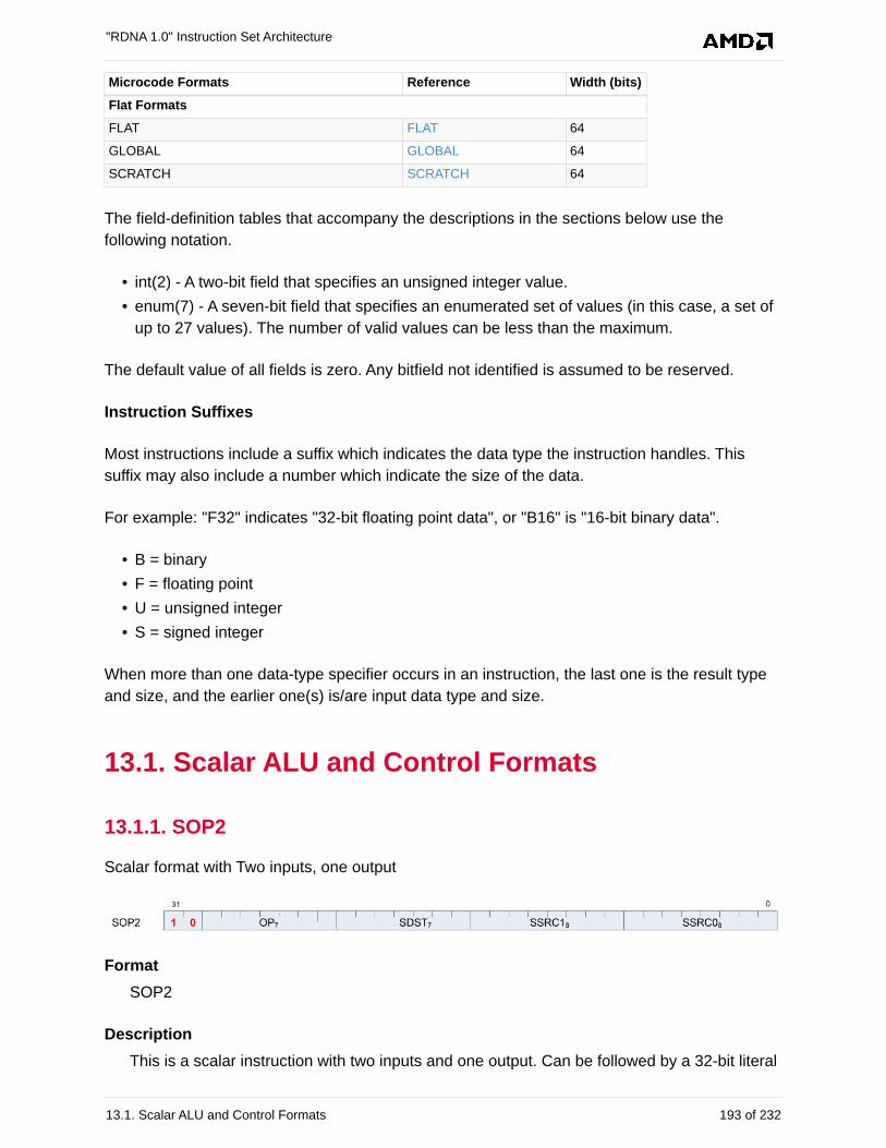
Microcode Formats Reference Width (bits)
Flat Formats
FLAT FLAT 64
GLOBAL GLOBAL 64
SCRATCH SCRATCH 64
The field-definition tables that accompany the descriptions in the sections below use the
following notation.
• int(2) - A two-bit field that specifies an unsigned integer value.
• enum(7) - A seven-bit field that specifies an enumerated set of values (in this case, a set of
up to 27 values). The number of valid values can be less than the maximum.
The default value of all fields is zero. Any bitfield not identified is assumed to be reserved.
Instruction Suffixes
Most instructions include a suffix which indicates the data type the instruction handles. This
suffix may also include a number which indicate the size of the data.
For example: "F32" indicates "32-bit floating point data", or "B16" is "16-bit binary data".
• B = binary
• F = floating point
• U = unsigned integer
• S = signed integer
When more than one data-type specifier occurs in an instruction, the last one is the result type
and size, and the earlier one(s) is/are input data type and size.
13.1. Scalar ALU and Control Formats
13.1.1. SOP2
Scalar format with Two inputs, one output
Format
SOP2
Description
This is a scalar instruction with two inputs and one output. Can be followed by a 32-bit literal
"RDNA 1.0" Instruction Set Architecture
13.1. Scalar ALU and Control Formats 193 of 232
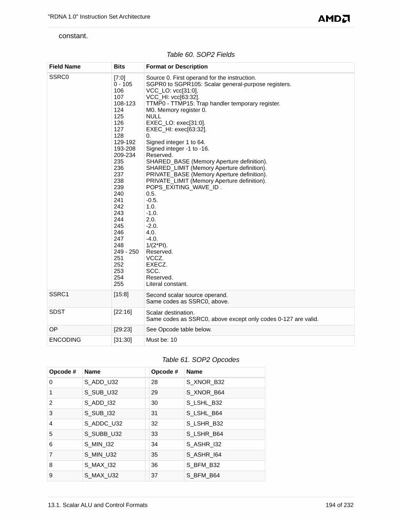
constant.
Table 60. SOP2 Fields
Field Name Bits Format or Description
SSRC0 [7:0]0 - 105106107108-123124125126127128129-192193-208209-234235236237238239240241242243244245246247248249 - 250251252253254255
Source 0. First operand for the instruction.SGPR0 to SGPR105: Scalar general-purpose registers.VCC_LO: vcc[31:0].VCC_HI: vcc[63:32].TTMP0 - TTMP15: Trap handler temporary register.M0. Memory register 0.NULLEXEC_LO: exec[31:0].EXEC_HI: exec[63:32].0.Signed integer 1 to 64.Signed integer -1 to -16.Reserved.SHARED_BASE (Memory Aperture definition).SHARED_LIMIT (Memory Aperture definition).PRIVATE_BASE (Memory Aperture definition).PRIVATE_LIMIT (Memory Aperture definition).POPS_EXITING_WAVE_ID .0.5.-0.5.1.0.-1.0.2.0.-2.0.4.0.-4.0.1/(2*PI).Reserved.VCCZ.EXECZ.SCC.Reserved.Literal constant.
SSRC1 [15:8] Second scalar source operand.Same codes as SSRC0, above.
SDST [22:16] Scalar destination.Same codes as SSRC0, above except only codes 0-127 are valid.
OP [29:23] See Opcode table below.
ENCODING [31:30] Must be: 10
Table 61. SOP2 Opcodes
Opcode # Name Opcode # Name
0 S_ADD_U32 28 S_XNOR_B32
1 S_SUB_U32 29 S_XNOR_B64
2 S_ADD_I32 30 S_LSHL_B32
3 S_SUB_I32 31 S_LSHL_B64
4 S_ADDC_U32 32 S_LSHR_B32
5 S_SUBB_U32 33 S_LSHR_B64
6 S_MIN_I32 34 S_ASHR_I32
7 S_MIN_U32 35 S_ASHR_I64
8 S_MAX_I32 36 S_BFM_B32
9 S_MAX_U32 37 S_BFM_B64
"RDNA 1.0" Instruction Set Architecture
13.1. Scalar ALU and Control Formats 194 of 232
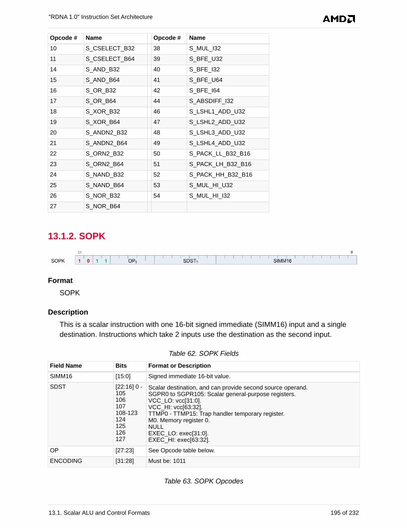
Opcode # Name Opcode # Name
10 S_CSELECT_B32 38 S_MUL_I32
11 S_CSELECT_B64 39 S_BFE_U32
14 S_AND_B32 40 S_BFE_I32
15 S_AND_B64 41 S_BFE_U64
16 S_OR_B32 42 S_BFE_I64
17 S_OR_B64 44 S_ABSDIFF_I32
18 S_XOR_B32 46 S_LSHL1_ADD_U32
19 S_XOR_B64 47 S_LSHL2_ADD_U32
20 S_ANDN2_B32 48 S_LSHL3_ADD_U32
21 S_ANDN2_B64 49 S_LSHL4_ADD_U32
22 S_ORN2_B32 50 S_PACK_LL_B32_B16
23 S_ORN2_B64 51 S_PACK_LH_B32_B16
24 S_NAND_B32 52 S_PACK_HH_B32_B16
25 S_NAND_B64 53 S_MUL_HI_U32
26 S_NOR_B32 54 S_MUL_HI_I32
27 S_NOR_B64
13.1.2. SOPK
Format
SOPK
Description
This is a scalar instruction with one 16-bit signed immediate (SIMM16) input and a single
destination. Instructions which take 2 inputs use the destination as the second input.
Table 62. SOPK Fields
Field Name Bits Format or Description
SIMM16 [15:0] Signed immediate 16-bit value.
SDST [22:16] 0 -105106107108-123124125126127
Scalar destination, and can provide second source operand.SGPR0 to SGPR105: Scalar general-purpose registers.VCC_LO: vcc[31:0].VCC_HI: vcc[63:32].TTMP0 - TTMP15: Trap handler temporary register.M0. Memory register 0.NULLEXEC_LO: exec[31:0].EXEC_HI: exec[63:32].
OP [27:23] See Opcode table below.
ENCODING [31:28] Must be: 1011
Table 63. SOPK Opcodes
"RDNA 1.0" Instruction Set Architecture
13.1. Scalar ALU and Control Formats 195 of 232
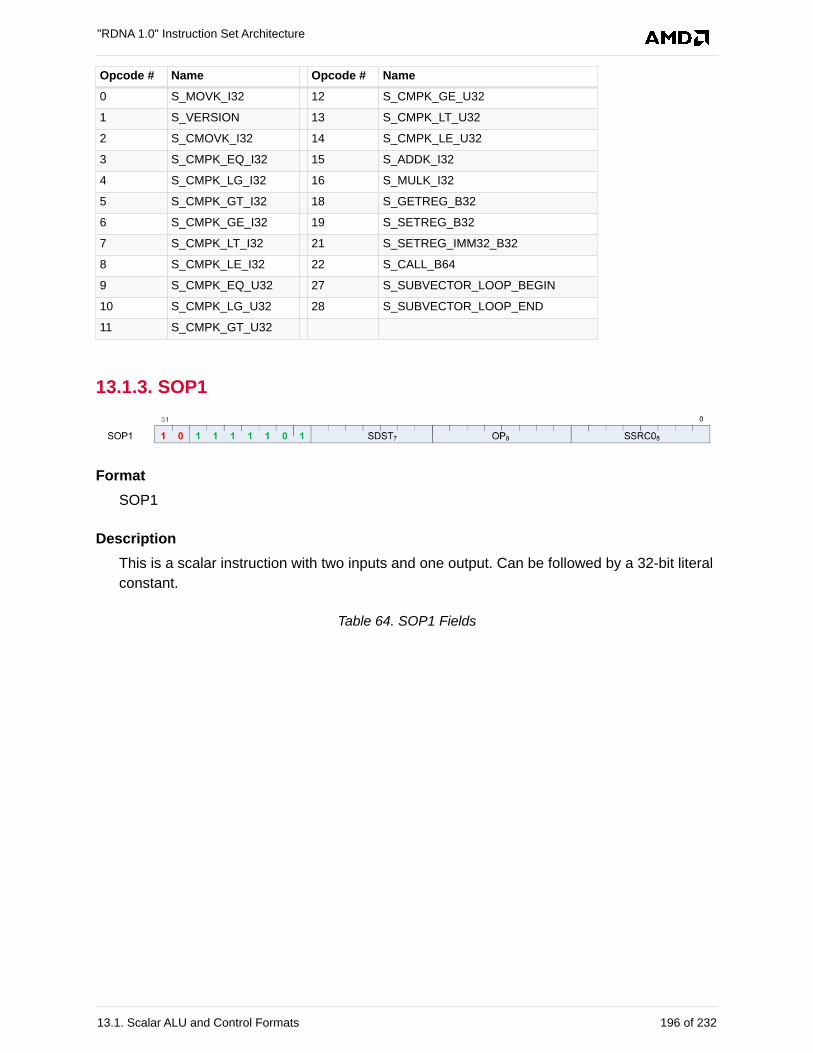
Opcode # Name Opcode # Name
0 S_MOVK_I32 12 S_CMPK_GE_U32
1 S_VERSION 13 S_CMPK_LT_U32
2 S_CMOVK_I32 14 S_CMPK_LE_U32
3 S_CMPK_EQ_I32 15 S_ADDK_I32
4 S_CMPK_LG_I32 16 S_MULK_I32
5 S_CMPK_GT_I32 18 S_GETREG_B32
6 S_CMPK_GE_I32 19 S_SETREG_B32
7 S_CMPK_LT_I32 21 S_SETREG_IMM32_B32
8 S_CMPK_LE_I32 22 S_CALL_B64
9 S_CMPK_EQ_U32 27 S_SUBVECTOR_LOOP_BEGIN
10 S_CMPK_LG_U32 28 S_SUBVECTOR_LOOP_END
11 S_CMPK_GT_U32
13.1.3. SOP1
Format
SOP1
Description
This is a scalar instruction with two inputs and one output. Can be followed by a 32-bit literal
constant.
Table 64. SOP1 Fields
"RDNA 1.0" Instruction Set Architecture
13.1. Scalar ALU and Control Formats 196 of 232
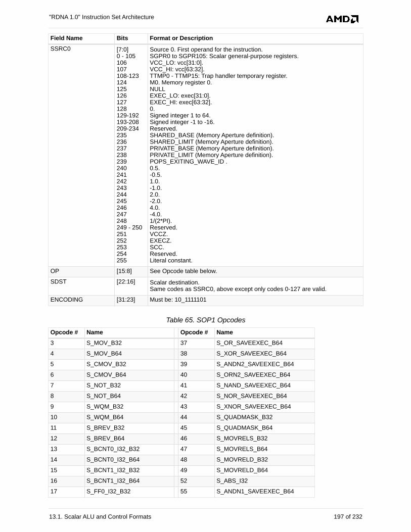
Field Name Bits Format or Description
SSRC0 [7:0]0 - 105106107108-123124125126127128129-192193-208209-234235236237238239240241242243244245246247248249 - 250251252253254255
Source 0. First operand for the instruction.SGPR0 to SGPR105: Scalar general-purpose registers.VCC_LO: vcc[31:0].VCC_HI: vcc[63:32].TTMP0 - TTMP15: Trap handler temporary register.M0. Memory register 0.NULLEXEC_LO: exec[31:0].EXEC_HI: exec[63:32].0.Signed integer 1 to 64.Signed integer -1 to -16.Reserved.SHARED_BASE (Memory Aperture definition).SHARED_LIMIT (Memory Aperture definition).PRIVATE_BASE (Memory Aperture definition).PRIVATE_LIMIT (Memory Aperture definition).POPS_EXITING_WAVE_ID .0.5.-0.5.1.0.-1.0.2.0.-2.0.4.0.-4.0.1/(2*PI).Reserved.VCCZ.EXECZ.SCC.Reserved.Literal constant.
OP [15:8] See Opcode table below.
SDST [22:16] Scalar destination.Same codes as SSRC0, above except only codes 0-127 are valid.
ENCODING [31:23] Must be: 10_1111101
Table 65. SOP1 Opcodes
Opcode # Name Opcode # Name
3 S_MOV_B32 37 S_OR_SAVEEXEC_B64
4 S_MOV_B64 38 S_XOR_SAVEEXEC_B64
5 S_CMOV_B32 39 S_ANDN2_SAVEEXEC_B64
6 S_CMOV_B64 40 S_ORN2_SAVEEXEC_B64
7 S_NOT_B32 41 S_NAND_SAVEEXEC_B64
8 S_NOT_B64 42 S_NOR_SAVEEXEC_B64
9 S_WQM_B32 43 S_XNOR_SAVEEXEC_B64
10 S_WQM_B64 44 S_QUADMASK_B32
11 S_BREV_B32 45 S_QUADMASK_B64
12 S_BREV_B64 46 S_MOVRELS_B32
13 S_BCNT0_I32_B32 47 S_MOVRELS_B64
14 S_BCNT0_I32_B64 48 S_MOVRELD_B32
15 S_BCNT1_I32_B32 49 S_MOVRELD_B64
16 S_BCNT1_I32_B64 52 S_ABS_I32
17 S_FF0_I32_B32 55 S_ANDN1_SAVEEXEC_B64
"RDNA 1.0" Instruction Set Architecture
13.1. Scalar ALU and Control Formats 197 of 232
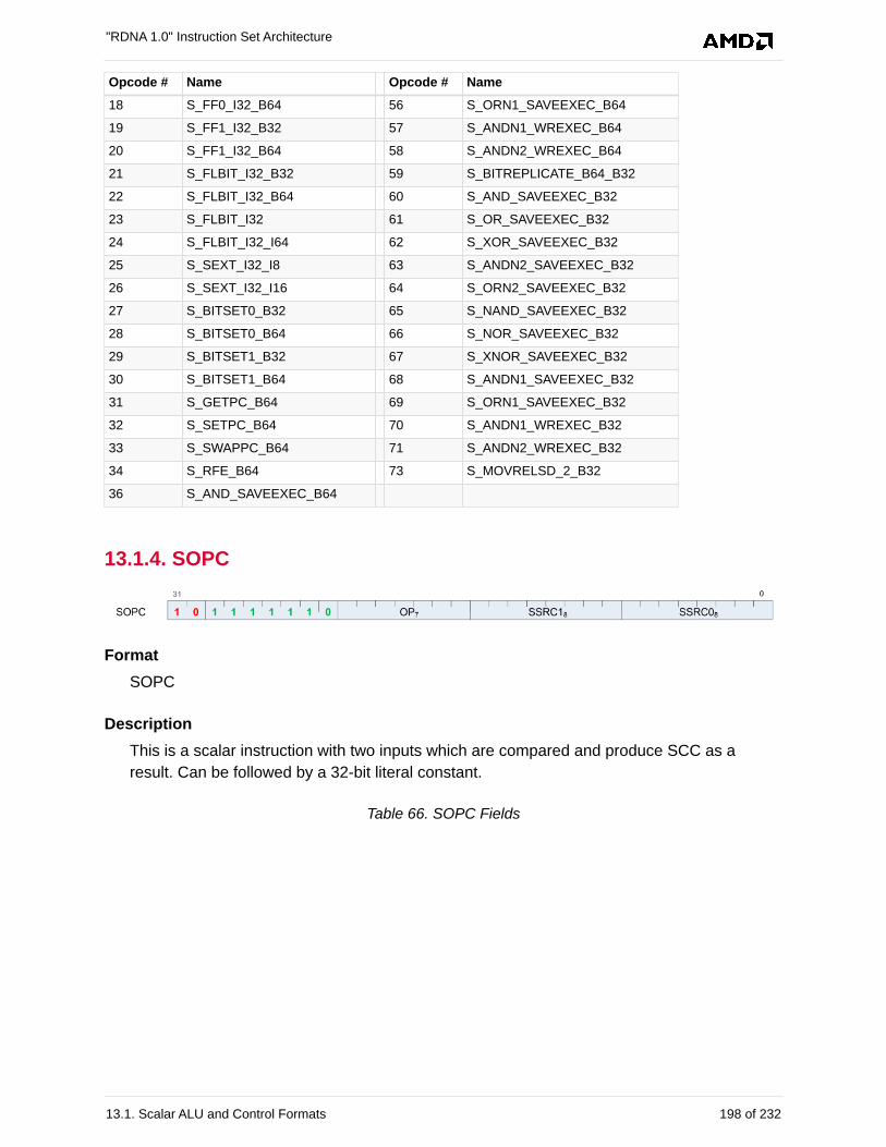
Opcode # Name Opcode # Name
18 S_FF0_I32_B64 56 S_ORN1_SAVEEXEC_B64
19 S_FF1_I32_B32 57 S_ANDN1_WREXEC_B64
20 S_FF1_I32_B64 58 S_ANDN2_WREXEC_B64
21 S_FLBIT_I32_B32 59 S_BITREPLICATE_B64_B32
22 S_FLBIT_I32_B64 60 S_AND_SAVEEXEC_B32
23 S_FLBIT_I32 61 S_OR_SAVEEXEC_B32
24 S_FLBIT_I32_I64 62 S_XOR_SAVEEXEC_B32
25 S_SEXT_I32_I8 63 S_ANDN2_SAVEEXEC_B32
26 S_SEXT_I32_I16 64 S_ORN2_SAVEEXEC_B32
27 S_BITSET0_B32 65 S_NAND_SAVEEXEC_B32
28 S_BITSET0_B64 66 S_NOR_SAVEEXEC_B32
29 S_BITSET1_B32 67 S_XNOR_SAVEEXEC_B32
30 S_BITSET1_B64 68 S_ANDN1_SAVEEXEC_B32
31 S_GETPC_B64 69 S_ORN1_SAVEEXEC_B32
32 S_SETPC_B64 70 S_ANDN1_WREXEC_B32
33 S_SWAPPC_B64 71 S_ANDN2_WREXEC_B32
34 S_RFE_B64 73 S_MOVRELSD_2_B32
36 S_AND_SAVEEXEC_B64
13.1.4. SOPC
Format
SOPC
Description
This is a scalar instruction with two inputs which are compared and produce SCC as a
result. Can be followed by a 32-bit literal constant.
Table 66. SOPC Fields
"RDNA 1.0" Instruction Set Architecture
13.1. Scalar ALU and Control Formats 198 of 232
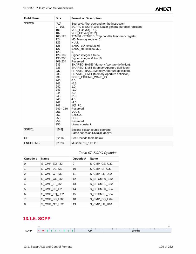
Field Name Bits Format or Description
SSRC0 [7:0]0 - 105106107108-123124125126127128129-192193-208209-234235236237238239240241242243244245246247248249 - 250251252253254255
Source 0. First operand for the instruction.SGPR0 to SGPR105: Scalar general-purpose registers.VCC_LO: vcc[31:0].VCC_HI: vcc[63:32].TTMP0 - TTMP15: Trap handler temporary register.M0. Memory register 0.NULLEXEC_LO: exec[31:0].EXEC_HI: exec[63:32].0.Signed integer 1 to 64.Signed integer -1 to -16.Reserved.SHARED_BASE (Memory Aperture definition).SHARED_LIMIT (Memory Aperture definition).PRIVATE_BASE (Memory Aperture definition).PRIVATE_LIMIT (Memory Aperture definition).POPS_EXITING_WAVE_ID .0.5.-0.5.1.0.-1.0.2.0.-2.0.4.0.-4.0.1/(2*PI).Reserved.VCCZ.EXECZ.SCC.Reserved.Literal constant.
SSRC1 [15:8] Second scalar source operand.Same codes as SSRC0, above.
OP [22:16] See Opcode table below.
ENCODING [31:23] Must be: 10_1111110
Table 67. SOPC Opcodes
Opcode # Name Opcode # Name
0 S_CMP_EQ_I32 9 S_CMP_GE_U32
1 S_CMP_LG_I32 10 S_CMP_LT_U32
2 S_CMP_GT_I32 11 S_CMP_LE_U32
3 S_CMP_GE_I32 12 S_BITCMP0_B32
4 S_CMP_LT_I32 13 S_BITCMP1_B32
5 S_CMP_LE_I32 14 S_BITCMP0_B64
6 S_CMP_EQ_U32 15 S_BITCMP1_B64
7 S_CMP_LG_U32 18 S_CMP_EQ_U64
8 S_CMP_GT_U32 19 S_CMP_LG_U64
13.1.5. SOPP
"RDNA 1.0" Instruction Set Architecture
13.1. Scalar ALU and Control Formats 199 of 232
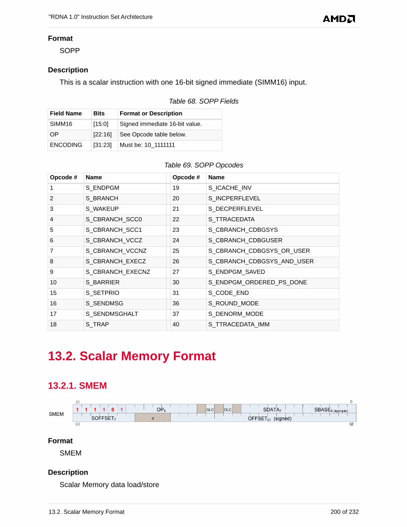
Format
SOPP
Description
This is a scalar instruction with one 16-bit signed immediate (SIMM16) input.
Table 68. SOPP Fields
Field Name Bits Format or Description
SIMM16 [15:0] Signed immediate 16-bit value.
OP [22:16] See Opcode table below.
ENCODING [31:23] Must be: 10_1111111
Table 69. SOPP Opcodes
Opcode # Name Opcode # Name
1 S_ENDPGM 19 S_ICACHE_INV
2 S_BRANCH 20 S_INCPERFLEVEL
3 S_WAKEUP 21 S_DECPERFLEVEL
4 S_CBRANCH_SCC0 22 S_TTRACEDATA
5 S_CBRANCH_SCC1 23 S_CBRANCH_CDBGSYS
6 S_CBRANCH_VCCZ 24 S_CBRANCH_CDBGUSER
7 S_CBRANCH_VCCNZ 25 S_CBRANCH_CDBGSYS_OR_USER
8 S_CBRANCH_EXECZ 26 S_CBRANCH_CDBGSYS_AND_USER
9 S_CBRANCH_EXECNZ 27 S_ENDPGM_SAVED
10 S_BARRIER 30 S_ENDPGM_ORDERED_PS_DONE
15 S_SETPRIO 31 S_CODE_END
16 S_SENDMSG 36 S_ROUND_MODE
17 S_SENDMSGHALT 37 S_DENORM_MODE
18 S_TRAP 40 S_TTRACEDATA_IMM
13.2. Scalar Memory Format
13.2.1. SMEM
Format
SMEM
Description
Scalar Memory data load/store
"RDNA 1.0" Instruction Set Architecture
13.2. Scalar Memory Format 200 of 232
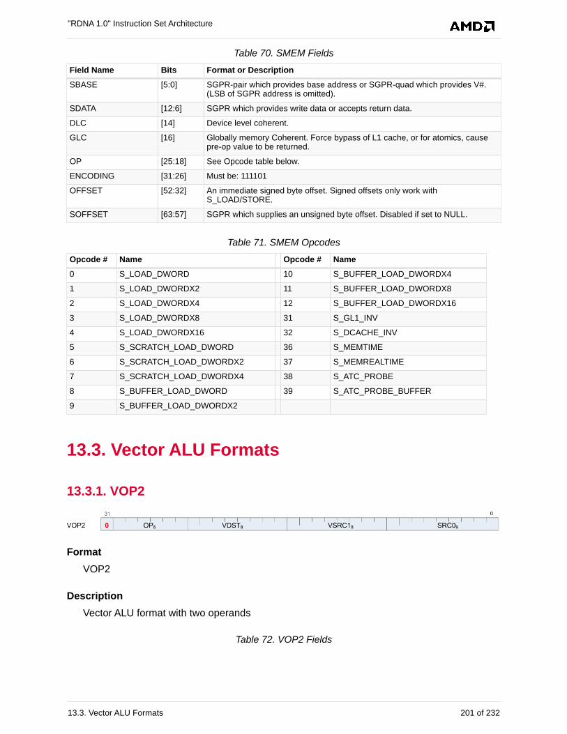
Table 70. SMEM Fields
Field Name Bits Format or Description
SBASE [5:0] SGPR-pair which provides base address or SGPR-quad which provides V#.(LSB of SGPR address is omitted).
SDATA [12:6] SGPR which provides write data or accepts return data.
DLC [14] Device level coherent.
GLC [16] Globally memory Coherent. Force bypass of L1 cache, or for atomics, causepre-op value to be returned.
OP [25:18] See Opcode table below.
ENCODING [31:26] Must be: 111101
OFFSET [52:32] An immediate signed byte offset. Signed offsets only work withS_LOAD/STORE.
SOFFSET [63:57] SGPR which supplies an unsigned byte offset. Disabled if set to NULL.
Table 71. SMEM Opcodes
Opcode # Name Opcode # Name
0 S_LOAD_DWORD 10 S_BUFFER_LOAD_DWORDX4
1 S_LOAD_DWORDX2 11 S_BUFFER_LOAD_DWORDX8
2 S_LOAD_DWORDX4 12 S_BUFFER_LOAD_DWORDX16
3 S_LOAD_DWORDX8 31 S_GL1_INV
4 S_LOAD_DWORDX16 32 S_DCACHE_INV
5 S_SCRATCH_LOAD_DWORD 36 S_MEMTIME
6 S_SCRATCH_LOAD_DWORDX2 37 S_MEMREALTIME
7 S_SCRATCH_LOAD_DWORDX4 38 S_ATC_PROBE
8 S_BUFFER_LOAD_DWORD 39 S_ATC_PROBE_BUFFER
9 S_BUFFER_LOAD_DWORDX2
13.3. Vector ALU Formats
13.3.1. VOP2
Format
VOP2
Description
Vector ALU format with two operands
Table 72. VOP2 Fields
"RDNA 1.0" Instruction Set Architecture
13.3. Vector ALU Formats 201 of 232
Field Name Bits Format or Description
SRC0 [8:0]0 - 105106107108-123124125126127128129-192193-208209-232233234235236237238239240241242243244245246247248249250251252253254255256 - 511
Source 0. First operand for the instruction.SGPR0 to SGPR105: Scalar general-purpose registers.VCC_LO: vcc[31:0].VCC_HI: vcc[63:32].TTMP0 - TTMP15: Trap handler temporary register.M0. Memory register 0.NULLEXEC_LO: exec[31:0].EXEC_HI: exec[63:32].0.Signed integer 1 to 64.Signed integer -1 to -16.Reserved.DPP8DPP8FISHARED_BASE (Memory Aperture definition).SHARED_LIMIT (Memory Aperture definition).PRIVATE_BASE (Memory Aperture definition).PRIVATE_LIMIT (Memory Aperture definition).POPS_EXITING_WAVE_ID .0.5.-0.5.1.0.-1.0.2.0.-2.0.4.0.-4.0.1/(2*PI).SDWADPP16VCCZ.EXECZ.SCC.Reserved.Literal constant.VGPR 0 - 255
VSRC1 [16:9] VGPR which provides the second operand.
VDST [24:17] Destination VGPR.
OP [30:25] See Opcode table below.
ENCODING [31] Must be: 0
Table 73. VOP2 Opcodes
Opcode # Name Opcode # Name
1 V_CNDMASK_B32 31 V_MAC_F32
3 V_ADD_F32 32 V_MADMK_F32
4 V_SUB_F32 33 V_MADAK_F32
5 V_SUBREV_F32 37 V_ADD_NC_U32
6 V_MAC_LEGACY_F32 38 V_SUB_NC_U32
7 V_MUL_LEGACY_F32 39 V_SUBREV_NC_U32
8 V_MUL_F32 40 V_ADD_CO_CI_U32
9 V_MUL_I32_I24 41 V_SUB_CO_CI_U32
10 V_MUL_HI_I32_I24 42 V_SUBREV_CO_CI_U32
11 V_MUL_U32_U24 43 V_FMAC_F32
12 V_MUL_HI_U32_U24 44 V_FMAMK_F32
15 V_MIN_F32 45 V_FMAAK_F32
"RDNA 1.0" Instruction Set Architecture
13.3. Vector ALU Formats 202 of 232
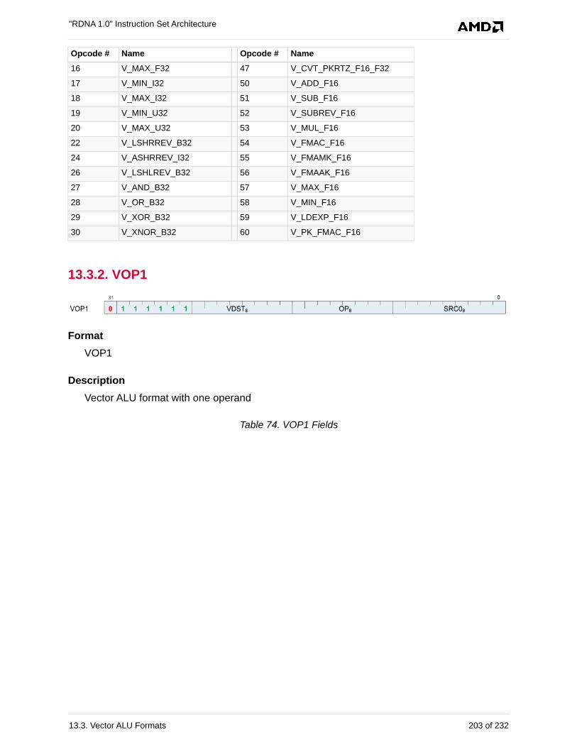
Opcode # Name Opcode # Name
16 V_MAX_F32 47 V_CVT_PKRTZ_F16_F32
17 V_MIN_I32 50 V_ADD_F16
18 V_MAX_I32 51 V_SUB_F16
19 V_MIN_U32 52 V_SUBREV_F16
20 V_MAX_U32 53 V_MUL_F16
22 V_LSHRREV_B32 54 V_FMAC_F16
24 V_ASHRREV_I32 55 V_FMAMK_F16
26 V_LSHLREV_B32 56 V_FMAAK_F16
27 V_AND_B32 57 V_MAX_F16
28 V_OR_B32 58 V_MIN_F16
29 V_XOR_B32 59 V_LDEXP_F16
30 V_XNOR_B32 60 V_PK_FMAC_F16
13.3.2. VOP1
Format
VOP1
Description
Vector ALU format with one operand
Table 74. VOP1 Fields
"RDNA 1.0" Instruction Set Architecture
13.3. Vector ALU Formats 203 of 232
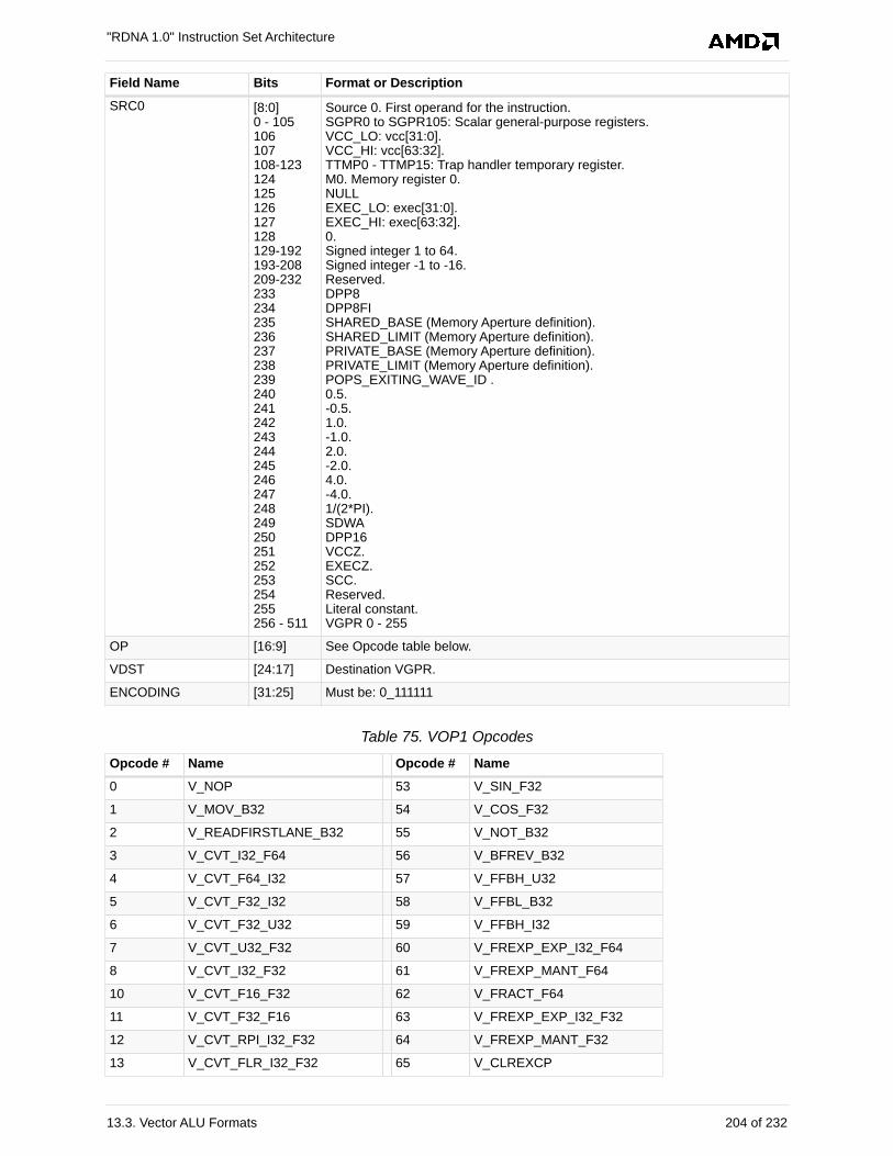
Field Name Bits Format or Description
SRC0 [8:0]0 - 105106107108-123124125126127128129-192193-208209-232233234235236237238239240241242243244245246247248249250251252253254255256 - 511
Source 0. First operand for the instruction.SGPR0 to SGPR105: Scalar general-purpose registers.VCC_LO: vcc[31:0].VCC_HI: vcc[63:32].TTMP0 - TTMP15: Trap handler temporary register.M0. Memory register 0.NULLEXEC_LO: exec[31:0].EXEC_HI: exec[63:32].0.Signed integer 1 to 64.Signed integer -1 to -16.Reserved.DPP8DPP8FISHARED_BASE (Memory Aperture definition).SHARED_LIMIT (Memory Aperture definition).PRIVATE_BASE (Memory Aperture definition).PRIVATE_LIMIT (Memory Aperture definition).POPS_EXITING_WAVE_ID .0.5.-0.5.1.0.-1.0.2.0.-2.0.4.0.-4.0.1/(2*PI).SDWADPP16VCCZ.EXECZ.SCC.Reserved.Literal constant.VGPR 0 - 255
OP [16:9] See Opcode table below.
VDST [24:17] Destination VGPR.
ENCODING [31:25] Must be: 0_111111
Table 75. VOP1 Opcodes
Opcode # Name Opcode # Name
0 V_NOP 53 V_SIN_F32
1 V_MOV_B32 54 V_COS_F32
2 V_READFIRSTLANE_B32 55 V_NOT_B32
3 V_CVT_I32_F64 56 V_BFREV_B32
4 V_CVT_F64_I32 57 V_FFBH_U32
5 V_CVT_F32_I32 58 V_FFBL_B32
6 V_CVT_F32_U32 59 V_FFBH_I32
7 V_CVT_U32_F32 60 V_FREXP_EXP_I32_F64
8 V_CVT_I32_F32 61 V_FREXP_MANT_F64
10 V_CVT_F16_F32 62 V_FRACT_F64
11 V_CVT_F32_F16 63 V_FREXP_EXP_I32_F32
12 V_CVT_RPI_I32_F32 64 V_FREXP_MANT_F32
13 V_CVT_FLR_I32_F32 65 V_CLREXCP
"RDNA 1.0" Instruction Set Architecture
13.3. Vector ALU Formats 204 of 232
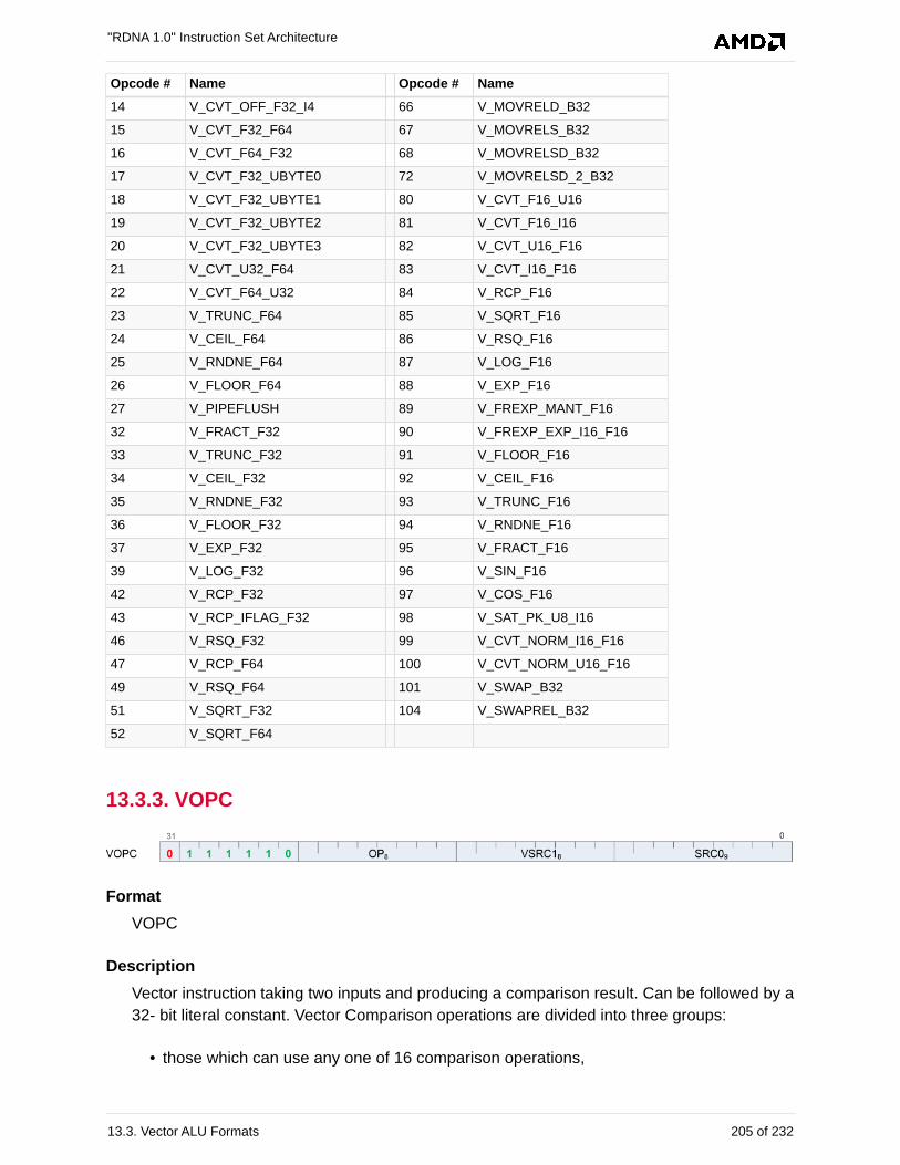
Opcode # Name Opcode # Name
14 V_CVT_OFF_F32_I4 66 V_MOVRELD_B32
15 V_CVT_F32_F64 67 V_MOVRELS_B32
16 V_CVT_F64_F32 68 V_MOVRELSD_B32
17 V_CVT_F32_UBYTE0 72 V_MOVRELSD_2_B32
18 V_CVT_F32_UBYTE1 80 V_CVT_F16_U16
19 V_CVT_F32_UBYTE2 81 V_CVT_F16_I16
20 V_CVT_F32_UBYTE3 82 V_CVT_U16_F16
21 V_CVT_U32_F64 83 V_CVT_I16_F16
22 V_CVT_F64_U32 84 V_RCP_F16
23 V_TRUNC_F64 85 V_SQRT_F16
24 V_CEIL_F64 86 V_RSQ_F16
25 V_RNDNE_F64 87 V_LOG_F16
26 V_FLOOR_F64 88 V_EXP_F16
27 V_PIPEFLUSH 89 V_FREXP_MANT_F16
32 V_FRACT_F32 90 V_FREXP_EXP_I16_F16
33 V_TRUNC_F32 91 V_FLOOR_F16
34 V_CEIL_F32 92 V_CEIL_F16
35 V_RNDNE_F32 93 V_TRUNC_F16
36 V_FLOOR_F32 94 V_RNDNE_F16
37 V_EXP_F32 95 V_FRACT_F16
39 V_LOG_F32 96 V_SIN_F16
42 V_RCP_F32 97 V_COS_F16
43 V_RCP_IFLAG_F32 98 V_SAT_PK_U8_I16
46 V_RSQ_F32 99 V_CVT_NORM_I16_F16
47 V_RCP_F64 100 V_CVT_NORM_U16_F16
49 V_RSQ_F64 101 V_SWAP_B32
51 V_SQRT_F32 104 V_SWAPREL_B32
52 V_SQRT_F64
13.3.3. VOPC
Format
VOPC
Description
Vector instruction taking two inputs and producing a comparison result. Can be followed by a
32- bit literal constant. Vector Comparison operations are divided into three groups:
• those which can use any one of 16 comparison operations,
"RDNA 1.0" Instruction Set Architecture
13.3. Vector ALU Formats 205 of 232
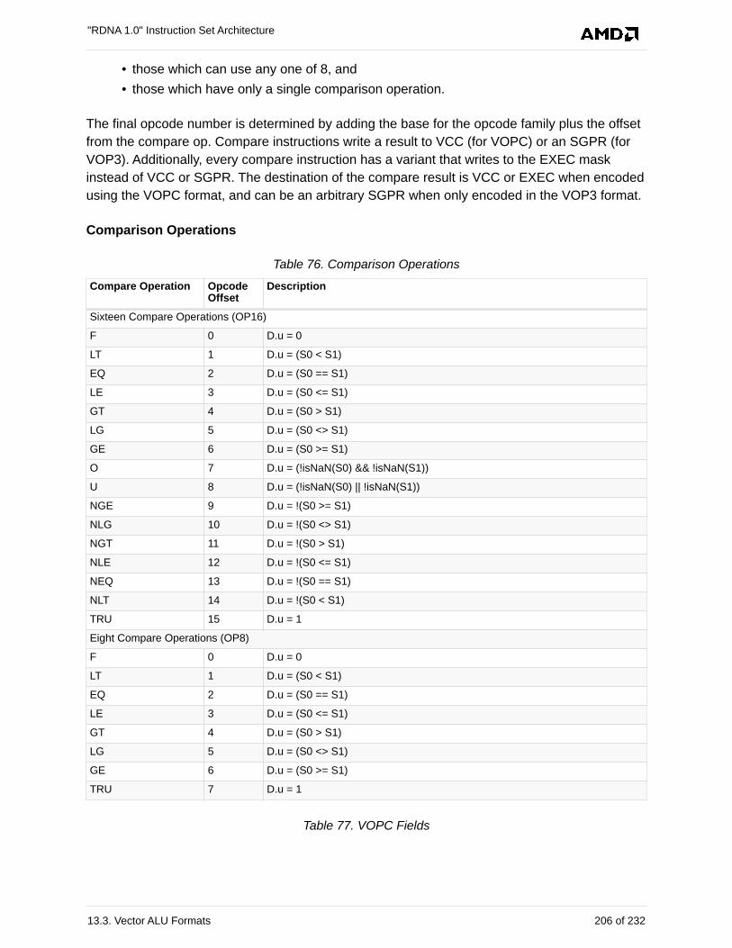
• those which can use any one of 8, and
• those which have only a single comparison operation.
The final opcode number is determined by adding the base for the opcode family plus the offset
from the compare op. Compare instructions write a result to VCC (for VOPC) or an SGPR (for
VOP3). Additionally, every compare instruction has a variant that writes to the EXEC mask
instead of VCC or SGPR. The destination of the compare result is VCC or EXEC when encoded
using the VOPC format, and can be an arbitrary SGPR when only encoded in the VOP3 format.
Comparison Operations
Table 76. Comparison Operations
Compare Operation OpcodeOffset
Description
Sixteen Compare Operations (OP16)
F 0 D.u = 0
LT 1 D.u = (S0 < S1)
EQ 2 D.u = (S0 == S1)
LE 3 D.u = (S0 <= S1)
GT 4 D.u = (S0 > S1)
LG 5 D.u = (S0 <> S1)
GE 6 D.u = (S0 >= S1)
O 7 D.u = (!isNaN(S0) && !isNaN(S1))
U 8 D.u = (!isNaN(S0) || !isNaN(S1))
NGE 9 D.u = !(S0 >= S1)
NLG 10 D.u = !(S0 <> S1)
NGT 11 D.u = !(S0 > S1)
NLE 12 D.u = !(S0 <= S1)
NEQ 13 D.u = !(S0 == S1)
NLT 14 D.u = !(S0 < S1)
TRU 15 D.u = 1
Eight Compare Operations (OP8)
F 0 D.u = 0
LT 1 D.u = (S0 < S1)
EQ 2 D.u = (S0 == S1)
LE 3 D.u = (S0 <= S1)
GT 4 D.u = (S0 > S1)
LG 5 D.u = (S0 <> S1)
GE 6 D.u = (S0 >= S1)
TRU 7 D.u = 1
Table 77. VOPC Fields
"RDNA 1.0" Instruction Set Architecture
13.3. Vector ALU Formats 206 of 232
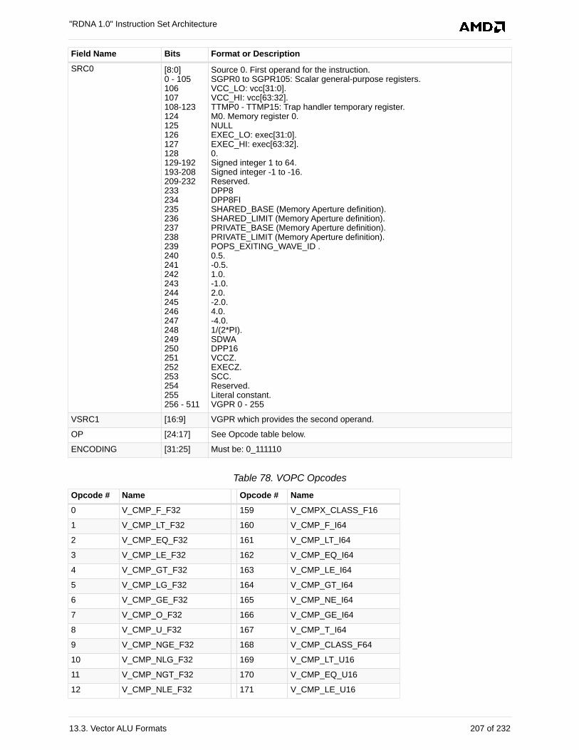
Field Name Bits Format or Description
SRC0 [8:0]0 - 105106107108-123124125126127128129-192193-208209-232233234235236237238239240241242243244245246247248249250251252253254255256 - 511
Source 0. First operand for the instruction.SGPR0 to SGPR105: Scalar general-purpose registers.VCC_LO: vcc[31:0].VCC_HI: vcc[63:32].TTMP0 - TTMP15: Trap handler temporary register.M0. Memory register 0.NULLEXEC_LO: exec[31:0].EXEC_HI: exec[63:32].0.Signed integer 1 to 64.Signed integer -1 to -16.Reserved.DPP8DPP8FISHARED_BASE (Memory Aperture definition).SHARED_LIMIT (Memory Aperture definition).PRIVATE_BASE (Memory Aperture definition).PRIVATE_LIMIT (Memory Aperture definition).POPS_EXITING_WAVE_ID .0.5.-0.5.1.0.-1.0.2.0.-2.0.4.0.-4.0.1/(2*PI).SDWADPP16VCCZ.EXECZ.SCC.Reserved.Literal constant.VGPR 0 - 255
VSRC1 [16:9] VGPR which provides the second operand.
OP [24:17] See Opcode table below.
ENCODING [31:25] Must be: 0_111110
Table 78. VOPC Opcodes
Opcode # Name Opcode # Name
0 V_CMP_F_F32 159 V_CMPX_CLASS_F16
1 V_CMP_LT_F32 160 V_CMP_F_I64
2 V_CMP_EQ_F32 161 V_CMP_LT_I64
3 V_CMP_LE_F32 162 V_CMP_EQ_I64
4 V_CMP_GT_F32 163 V_CMP_LE_I64
5 V_CMP_LG_F32 164 V_CMP_GT_I64
6 V_CMP_GE_F32 165 V_CMP_NE_I64
7 V_CMP_O_F32 166 V_CMP_GE_I64
8 V_CMP_U_F32 167 V_CMP_T_I64
9 V_CMP_NGE_F32 168 V_CMP_CLASS_F64
10 V_CMP_NLG_F32 169 V_CMP_LT_U16
11 V_CMP_NGT_F32 170 V_CMP_EQ_U16
12 V_CMP_NLE_F32 171 V_CMP_LE_U16
"RDNA 1.0" Instruction Set Architecture
13.3. Vector ALU Formats 207 of 232
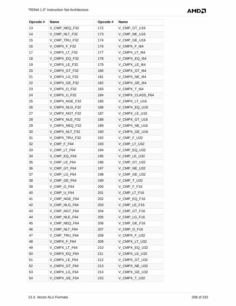
Opcode # Name Opcode # Name
13 V_CMP_NEQ_F32 172 V_CMP_GT_U16
14 V_CMP_NLT_F32 173 V_CMP_NE_U16
15 V_CMP_TRU_F32 174 V_CMP_GE_U16
16 V_CMPX_F_F32 176 V_CMPX_F_I64
17 V_CMPX_LT_F32 177 V_CMPX_LT_I64
18 V_CMPX_EQ_F32 178 V_CMPX_EQ_I64
19 V_CMPX_LE_F32 179 V_CMPX_LE_I64
20 V_CMPX_GT_F32 180 V_CMPX_GT_I64
21 V_CMPX_LG_F32 181 V_CMPX_NE_I64
22 V_CMPX_GE_F32 182 V_CMPX_GE_I64
23 V_CMPX_O_F32 183 V_CMPX_T_I64
24 V_CMPX_U_F32 184 V_CMPX_CLASS_F64
25 V_CMPX_NGE_F32 185 V_CMPX_LT_U16
26 V_CMPX_NLG_F32 186 V_CMPX_EQ_U16
27 V_CMPX_NGT_F32 187 V_CMPX_LE_U16
28 V_CMPX_NLE_F32 188 V_CMPX_GT_U16
29 V_CMPX_NEQ_F32 189 V_CMPX_NE_U16
30 V_CMPX_NLT_F32 190 V_CMPX_GE_U16
31 V_CMPX_TRU_F32 192 V_CMP_F_U32
32 V_CMP_F_F64 193 V_CMP_LT_U32
33 V_CMP_LT_F64 194 V_CMP_EQ_U32
34 V_CMP_EQ_F64 195 V_CMP_LE_U32
35 V_CMP_LE_F64 196 V_CMP_GT_U32
36 V_CMP_GT_F64 197 V_CMP_NE_U32
37 V_CMP_LG_F64 198 V_CMP_GE_U32
38 V_CMP_GE_F64 199 V_CMP_T_U32
39 V_CMP_O_F64 200 V_CMP_F_F16
40 V_CMP_U_F64 201 V_CMP_LT_F16
41 V_CMP_NGE_F64 202 V_CMP_EQ_F16
42 V_CMP_NLG_F64 203 V_CMP_LE_F16
43 V_CMP_NGT_F64 204 V_CMP_GT_F16
44 V_CMP_NLE_F64 205 V_CMP_LG_F16
45 V_CMP_NEQ_F64 206 V_CMP_GE_F16
46 V_CMP_NLT_F64 207 V_CMP_O_F16
47 V_CMP_TRU_F64 208 V_CMPX_F_U32
48 V_CMPX_F_F64 209 V_CMPX_LT_U32
49 V_CMPX_LT_F64 210 V_CMPX_EQ_U32
50 V_CMPX_EQ_F64 211 V_CMPX_LE_U32
51 V_CMPX_LE_F64 212 V_CMPX_GT_U32
52 V_CMPX_GT_F64 213 V_CMPX_NE_U32
53 V_CMPX_LG_F64 214 V_CMPX_GE_U32
54 V_CMPX_GE_F64 215 V_CMPX_T_U32
"RDNA 1.0" Instruction Set Architecture
13.3. Vector ALU Formats 208 of 232
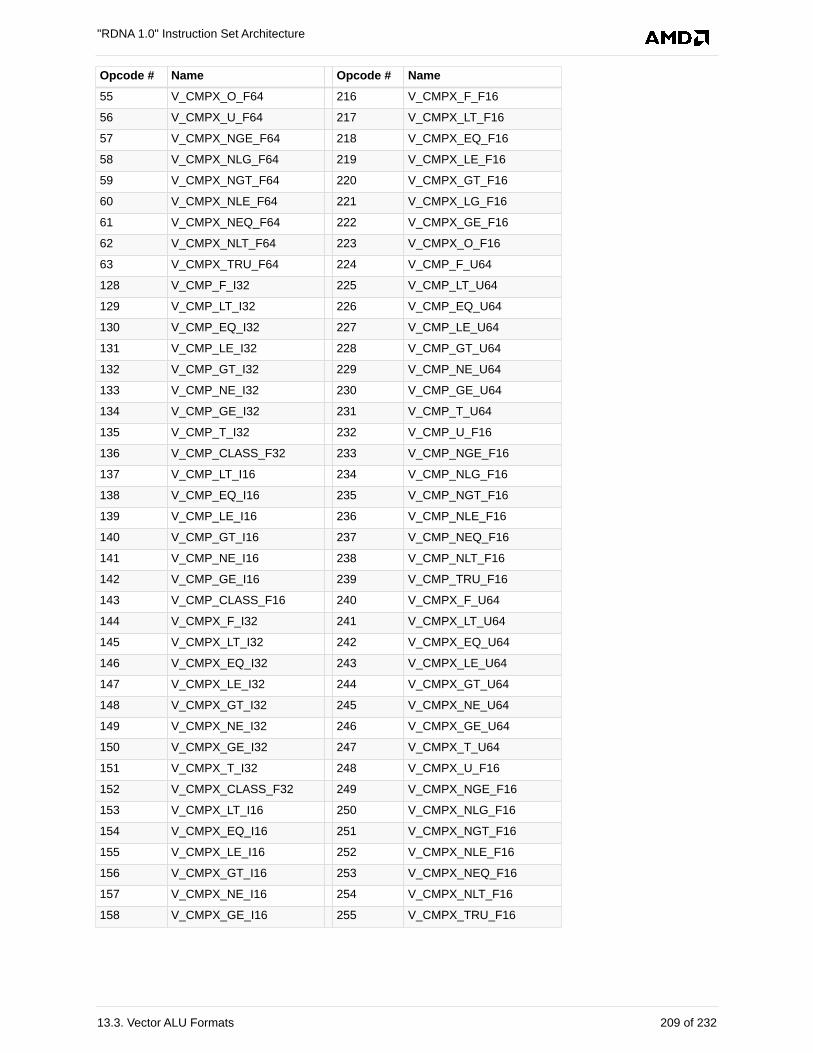
Opcode # Name Opcode # Name
55 V_CMPX_O_F64 216 V_CMPX_F_F16
56 V_CMPX_U_F64 217 V_CMPX_LT_F16
57 V_CMPX_NGE_F64 218 V_CMPX_EQ_F16
58 V_CMPX_NLG_F64 219 V_CMPX_LE_F16
59 V_CMPX_NGT_F64 220 V_CMPX_GT_F16
60 V_CMPX_NLE_F64 221 V_CMPX_LG_F16
61 V_CMPX_NEQ_F64 222 V_CMPX_GE_F16
62 V_CMPX_NLT_F64 223 V_CMPX_O_F16
63 V_CMPX_TRU_F64 224 V_CMP_F_U64
128 V_CMP_F_I32 225 V_CMP_LT_U64
129 V_CMP_LT_I32 226 V_CMP_EQ_U64
130 V_CMP_EQ_I32 227 V_CMP_LE_U64
131 V_CMP_LE_I32 228 V_CMP_GT_U64
132 V_CMP_GT_I32 229 V_CMP_NE_U64
133 V_CMP_NE_I32 230 V_CMP_GE_U64
134 V_CMP_GE_I32 231 V_CMP_T_U64
135 V_CMP_T_I32 232 V_CMP_U_F16
136 V_CMP_CLASS_F32 233 V_CMP_NGE_F16
137 V_CMP_LT_I16 234 V_CMP_NLG_F16
138 V_CMP_EQ_I16 235 V_CMP_NGT_F16
139 V_CMP_LE_I16 236 V_CMP_NLE_F16
140 V_CMP_GT_I16 237 V_CMP_NEQ_F16
141 V_CMP_NE_I16 238 V_CMP_NLT_F16
142 V_CMP_GE_I16 239 V_CMP_TRU_F16
143 V_CMP_CLASS_F16 240 V_CMPX_F_U64
144 V_CMPX_F_I32 241 V_CMPX_LT_U64
145 V_CMPX_LT_I32 242 V_CMPX_EQ_U64
146 V_CMPX_EQ_I32 243 V_CMPX_LE_U64
147 V_CMPX_LE_I32 244 V_CMPX_GT_U64
148 V_CMPX_GT_I32 245 V_CMPX_NE_U64
149 V_CMPX_NE_I32 246 V_CMPX_GE_U64
150 V_CMPX_GE_I32 247 V_CMPX_T_U64
151 V_CMPX_T_I32 248 V_CMPX_U_F16
152 V_CMPX_CLASS_F32 249 V_CMPX_NGE_F16
153 V_CMPX_LT_I16 250 V_CMPX_NLG_F16
154 V_CMPX_EQ_I16 251 V_CMPX_NGT_F16
155 V_CMPX_LE_I16 252 V_CMPX_NLE_F16
156 V_CMPX_GT_I16 253 V_CMPX_NEQ_F16
157 V_CMPX_NE_I16 254 V_CMPX_NLT_F16
158 V_CMPX_GE_I16 255 V_CMPX_TRU_F16
"RDNA 1.0" Instruction Set Architecture
13.3. Vector ALU Formats 209 of 232
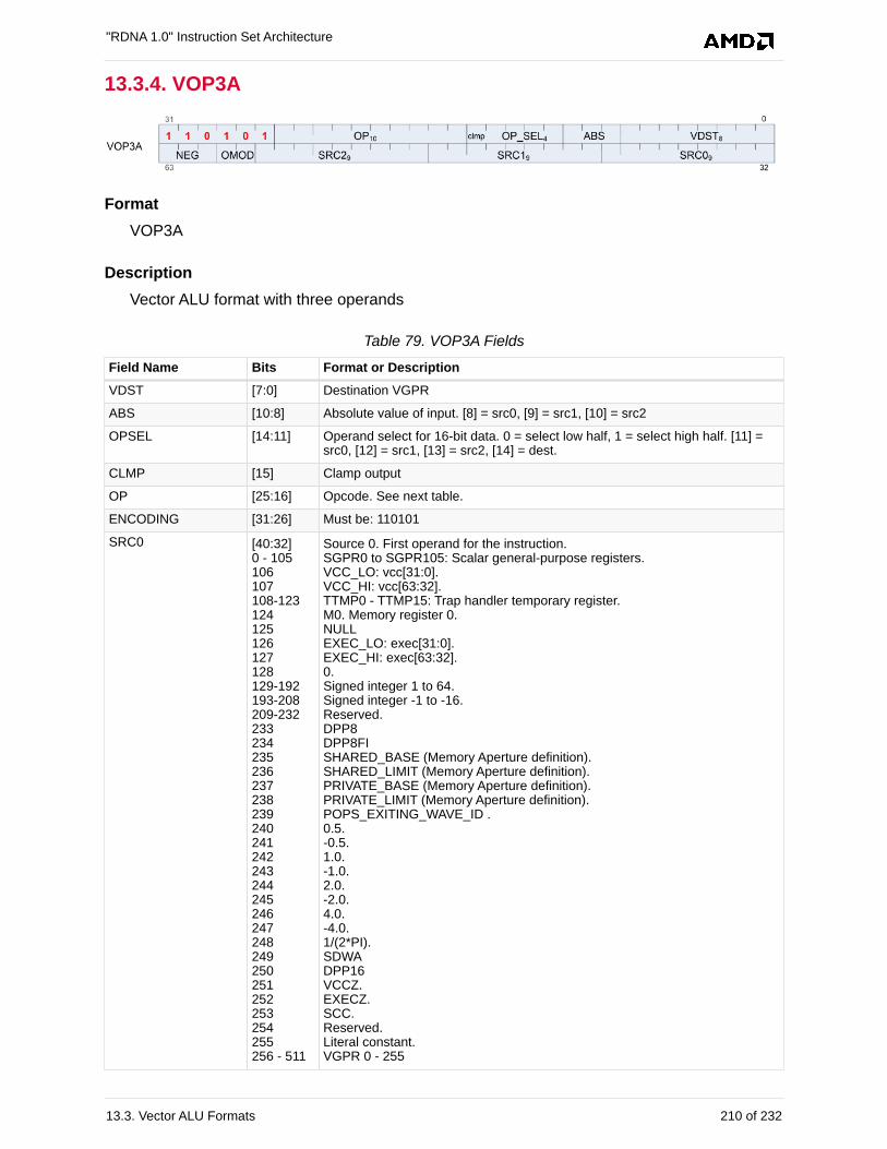
13.3.4. VOP3A
Format
VOP3A
Description
Vector ALU format with three operands
Table 79. VOP3A Fields
Field Name Bits Format or Description
VDST [7:0] Destination VGPR
ABS [10:8] Absolute value of input. [8] = src0, [9] = src1, [10] = src2
OPSEL [14:11] Operand select for 16-bit data. 0 = select low half, 1 = select high half. [11] =src0, [12] = src1, [13] = src2, [14] = dest.
CLMP [15] Clamp output
OP [25:16] Opcode. See next table.
ENCODING [31:26] Must be: 110101
SRC0 [40:32]0 - 105106107108-123124125126127128129-192193-208209-232233234235236237238239240241242243244245246247248249250251252253254255256 - 511
Source 0. First operand for the instruction.SGPR0 to SGPR105: Scalar general-purpose registers.VCC_LO: vcc[31:0].VCC_HI: vcc[63:32].TTMP0 - TTMP15: Trap handler temporary register.M0. Memory register 0.NULLEXEC_LO: exec[31:0].EXEC_HI: exec[63:32].0.Signed integer 1 to 64.Signed integer -1 to -16.Reserved.DPP8DPP8FISHARED_BASE (Memory Aperture definition).SHARED_LIMIT (Memory Aperture definition).PRIVATE_BASE (Memory Aperture definition).PRIVATE_LIMIT (Memory Aperture definition).POPS_EXITING_WAVE_ID .0.5.-0.5.1.0.-1.0.2.0.-2.0.4.0.-4.0.1/(2*PI).SDWADPP16VCCZ.EXECZ.SCC.Reserved.Literal constant.VGPR 0 - 255
"RDNA 1.0" Instruction Set Architecture
13.3. Vector ALU Formats 210 of 232
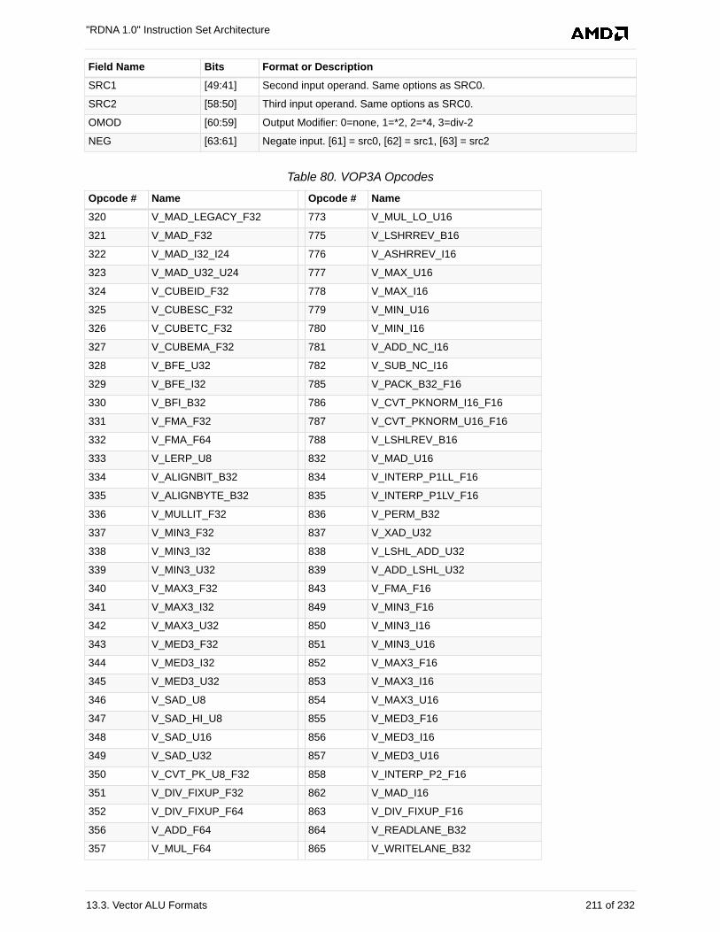
Field Name Bits Format or Description
SRC1 [49:41] Second input operand. Same options as SRC0.
SRC2 [58:50] Third input operand. Same options as SRC0.
OMOD [60:59] Output Modifier: 0=none, 1=*2, 2=*4, 3=div-2
NEG [63:61] Negate input. [61] = src0, [62] = src1, [63] = src2
Table 80. VOP3A Opcodes
Opcode # Name Opcode # Name
320 V_MAD_LEGACY_F32 773 V_MUL_LO_U16
321 V_MAD_F32 775 V_LSHRREV_B16
322 V_MAD_I32_I24 776 V_ASHRREV_I16
323 V_MAD_U32_U24 777 V_MAX_U16
324 V_CUBEID_F32 778 V_MAX_I16
325 V_CUBESC_F32 779 V_MIN_U16
326 V_CUBETC_F32 780 V_MIN_I16
327 V_CUBEMA_F32 781 V_ADD_NC_I16
328 V_BFE_U32 782 V_SUB_NC_I16
329 V_BFE_I32 785 V_PACK_B32_F16
330 V_BFI_B32 786 V_CVT_PKNORM_I16_F16
331 V_FMA_F32 787 V_CVT_PKNORM_U16_F16
332 V_FMA_F64 788 V_LSHLREV_B16
333 V_LERP_U8 832 V_MAD_U16
334 V_ALIGNBIT_B32 834 V_INTERP_P1LL_F16
335 V_ALIGNBYTE_B32 835 V_INTERP_P1LV_F16
336 V_MULLIT_F32 836 V_PERM_B32
337 V_MIN3_F32 837 V_XAD_U32
338 V_MIN3_I32 838 V_LSHL_ADD_U32
339 V_MIN3_U32 839 V_ADD_LSHL_U32
340 V_MAX3_F32 843 V_FMA_F16
341 V_MAX3_I32 849 V_MIN3_F16
342 V_MAX3_U32 850 V_MIN3_I16
343 V_MED3_F32 851 V_MIN3_U16
344 V_MED3_I32 852 V_MAX3_F16
345 V_MED3_U32 853 V_MAX3_I16
346 V_SAD_U8 854 V_MAX3_U16
347 V_SAD_HI_U8 855 V_MED3_F16
348 V_SAD_U16 856 V_MED3_I16
349 V_SAD_U32 857 V_MED3_U16
350 V_CVT_PK_U8_F32 858 V_INTERP_P2_F16
351 V_DIV_FIXUP_F32 862 V_MAD_I16
352 V_DIV_FIXUP_F64 863 V_DIV_FIXUP_F16
356 V_ADD_F64 864 V_READLANE_B32
357 V_MUL_F64 865 V_WRITELANE_B32
"RDNA 1.0" Instruction Set Architecture
13.3. Vector ALU Formats 211 of 232
Opcode # Name Opcode # Name
358 V_MIN_F64 866 V_LDEXP_F32
359 V_MAX_F64 867 V_BFM_B32
360 V_LDEXP_F64 868 V_BCNT_U32_B32
361 V_MUL_LO_U32 869 V_MBCNT_LO_U32_B32
362 V_MUL_HI_U32 870 V_MBCNT_HI_U32_B32
364 V_MUL_HI_I32 872 V_CVT_PKNORM_I16_F32
367 V_DIV_FMAS_F32 873 V_CVT_PKNORM_U16_F32
368 V_DIV_FMAS_F64 874 V_CVT_PK_U16_U32
369 V_MSAD_U8 875 V_CVT_PK_I16_I32
370 V_QSAD_PK_U16_U8 877 V_ADD3_U32
371 V_MQSAD_PK_U16_U8 879 V_LSHL_OR_B32
372 V_TRIG_PREOP_F64 881 V_AND_OR_B32
373 V_MQSAD_U32_U8 882 V_OR3_B32
376 V_XOR3_B32 883 V_MAD_U32_U16
767 V_LSHLREV_B64 885 V_MAD_I32_I16
768 V_LSHRREV_B64 886 V_SUB_NC_I32
769 V_ASHRREV_I64 887 V_PERMLANE16_B32
771 V_ADD_NC_U16 888 V_PERMLANEX16_B32
772 V_SUB_NC_U16 895 V_ADD_NC_I32
13.3.5. VOP3B
Format
VOP3B
Description
Vector ALU format with three operands and a scalar result. This encoding is used only for a
few opcodes.
This encoding allows specifying a unique scalar destination, and is used only for the opcodes
listed below. All other opcodes use VOP3A.
• V_ADD_CO_U32
• V_SUB_CO_U32
• V_SUBREV_CO_U32
• V_ADDC_CO_U32
• V_SUBB_CO_U32
• V_SUBBREV_CO_U32
"RDNA 1.0" Instruction Set Architecture
13.3. Vector ALU Formats 212 of 232
• V_DIV_SCALE_F32
• V_DIV_SCALE_F64
• V_MAD_U64_U32
• V_MAD_I64_I32
Table 81. VOP3B Fields
Field Name Bits Format or Description
VDST [7:0] Destination VGPR
SDST [14:8] Scalar destination
CLMP [15] Clamp result
OP [25:16] Opcode. see next table.
ENCODING [31:26] Must be: 110101
SRC0 [40:32]0 - 105106107108-123124125126127128129-192193-208209-232233234235236237238239240241242243244245246247248249250251252253254255256 - 511
Source 0. First operand for the instruction.SGPR0 to SGPR105: Scalar general-purpose registers.VCC_LO: vcc[31:0].VCC_HI: vcc[63:32].TTMP0 - TTMP15: Trap handler temporary register.M0. Memory register 0.NULLEXEC_LO: exec[31:0].EXEC_HI: exec[63:32].0.Signed integer 1 to 64.Signed integer -1 to -16.Reserved.DPP8DPP8FISHARED_BASE (Memory Aperture definition).SHARED_LIMIT (Memory Aperture definition).PRIVATE_BASE (Memory Aperture definition).PRIVATE_LIMIT (Memory Aperture definition).POPS_EXITING_WAVE_ID .0.5.-0.5.1.0.-1.0.2.0.-2.0.4.0.-4.0.1/(2*PI).SDWADPP16VCCZ.EXECZ.SCC.Reserved.Literal constant.VGPR 0 - 255
SRC1 [49:41] Second input operand. Same options as SRC0.
SRC2 [58:50] Third input operand. Same options as SRC0.
OMOD [60:59] Output Modifier: 0=none, 1=*2, 2=*4, 3=div-2
NEG [63:61] Negate input. [61] = src0, [62] = src1, [63] = src2
Table 82. VOP3B Opcodes
"RDNA 1.0" Instruction Set Architecture
13.3. Vector ALU Formats 213 of 232
Opcode # Name Opcode # Name
365 V_DIV_SCALE_F32 783 V_ADD_CO_U32
366 V_DIV_SCALE_F64 784 V_SUB_CO_U32
374 V_MAD_U64_U32 793 V_SUBREV_CO_U32
375 V_MAD_I64_I32
13.3.6. VOP3P
Format
VOP3P
Description
Vector ALU format taking one, two or three pairs of 16 bit inputs and producing two 16-bit
outputs (packed into 1 dword).
Table 83. VOP3P Fields
Field Name Bits Format or Description
VDST [7:0] Destination VGPR
NEG_HI [10:8] Negate sources 0,1,2 of the high 16-bits.
OPSEL [13:11] Select low or high for low sources 0=[11], 1=[12], 2=[13].
OPSEL_HI2 [14] Select low or high for high sources 0=[14], 1=[60], 2=[59].
CLMP [15] 1 = clamp result.
OP [22:16] Opcode. see next table.
ENCODING [31:26] Must be: 110011
"RDNA 1.0" Instruction Set Architecture
13.3. Vector ALU Formats 214 of 232
Field Name Bits Format or Description
SRC0 [40:32]0 - 105106107108-123124125126127128129-192193-208209-232233234235236237238239240241242243244245246247248249250251252253254255256 - 511
Source 0. First operand for the instruction.SGPR0 to SGPR105: Scalar general-purpose registers.VCC_LO: vcc[31:0].VCC_HI: vcc[63:32].TTMP0 - TTMP15: Trap handler temporary register.M0. Memory register 0.NULLEXEC_LO: exec[31:0].EXEC_HI: exec[63:32].0.Signed integer 1 to 64.Signed integer -1 to -16.Reserved.DPP8DPP8FISHARED_BASE (Memory Aperture definition).SHARED_LIMIT (Memory Aperture definition).PRIVATE_BASE (Memory Aperture definition).PRIVATE_LIMIT (Memory Aperture definition).POPS_EXITING_WAVE_ID .0.5.-0.5.1.0.-1.0.2.0.-2.0.4.0.-4.0.1/(2*PI).SDWADPP16VCCZ.EXECZ.SCC.Reserved.Literal constant.VGPR 0 - 255
SRC1 [49:41] Second input operand. Same options as SRC0.
SRC2 [58:50] Third input operand. Same options as SRC0.
OPSEL_HI [60:59] See OP_SEL_HI2.
NEG [63:61] Negate input for low 16-bits of sources. [61] = src0, [62] = src1, [63] = src2
Table 84. VOP3P Opcodes
Opcode # Name Opcode # Name
0 V_PK_MAD_I16 11 V_PK_SUB_U16
1 V_PK_MUL_LO_U16 12 V_PK_MAX_U16
2 V_PK_ADD_I16 13 V_PK_MIN_U16
3 V_PK_SUB_I16 14 V_PK_FMA_F16
4 V_PK_LSHLREV_B16 15 V_PK_ADD_F16
5 V_PK_LSHRREV_B16 16 V_PK_MUL_F16
6 V_PK_ASHRREV_I16 17 V_PK_MIN_F16
7 V_PK_MAX_I16 18 V_PK_MAX_F16
8 V_PK_MIN_I16 32 V_FMA_MIX_F32
9 V_PK_MAD_U16 33 V_FMA_MIXLO_F16
10 V_PK_ADD_U16 34 V_FMA_MIXHI_F16
"RDNA 1.0" Instruction Set Architecture
13.3. Vector ALU Formats 215 of 232
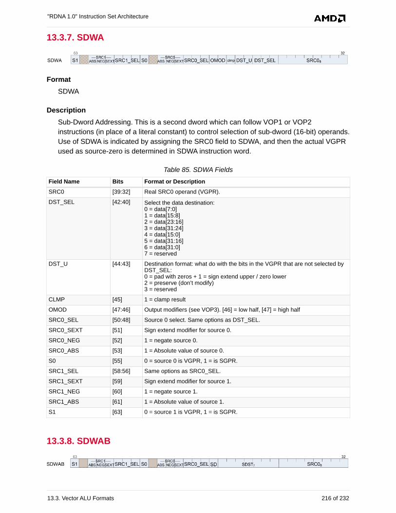
13.3.7. SDWA
Format
SDWA
Description
Sub-Dword Addressing. This is a second dword which can follow VOP1 or VOP2
instructions (in place of a literal constant) to control selection of sub-dword (16-bit) operands.
Use of SDWA is indicated by assigning the SRC0 field to SDWA, and then the actual VGPR
used as source-zero is determined in SDWA instruction word.
Table 85. SDWA Fields
Field Name Bits Format or Description
SRC0 [39:32] Real SRC0 operand (VGPR).
DST_SEL [42:40] Select the data destination:0 = data[7:0] 1 = data[15:8] 2 = data[23:16] 3 = data[31:24]4 = data[15:0] 5 = data[31:16] 6 = data[31:0] 7 = reserved
DST_U [44:43] Destination format: what do with the bits in the VGPR that are not selected byDST_SEL:0 = pad with zeros + 1 = sign extend upper / zero lower2 = preserve (don’t modify)3 = reserved
CLMP [45] 1 = clamp result
OMOD [47:46] Output modifiers (see VOP3). [46] = low half, [47] = high half
SRC0_SEL [50:48] Source 0 select. Same options as DST_SEL.
SRC0_SEXT [51] Sign extend modifier for source 0.
SRC0_NEG [52] 1 = negate source 0.
SRC0_ABS [53] 1 = Absolute value of source 0.
S0 [55] 0 = source 0 is VGPR, 1 = is SGPR.
SRC1_SEL [58:56] Same options as SRC0_SEL.
SRC1_SEXT [59] Sign extend modifier for source 1.
SRC1_NEG [60] 1 = negate source 1.
SRC1_ABS [61] 1 = Absolute value of source 1.
S1 [63] 0 = source 1 is VGPR, 1 = is SGPR.
13.3.8. SDWAB
"RDNA 1.0" Instruction Set Architecture
13.3. Vector ALU Formats 216 of 232
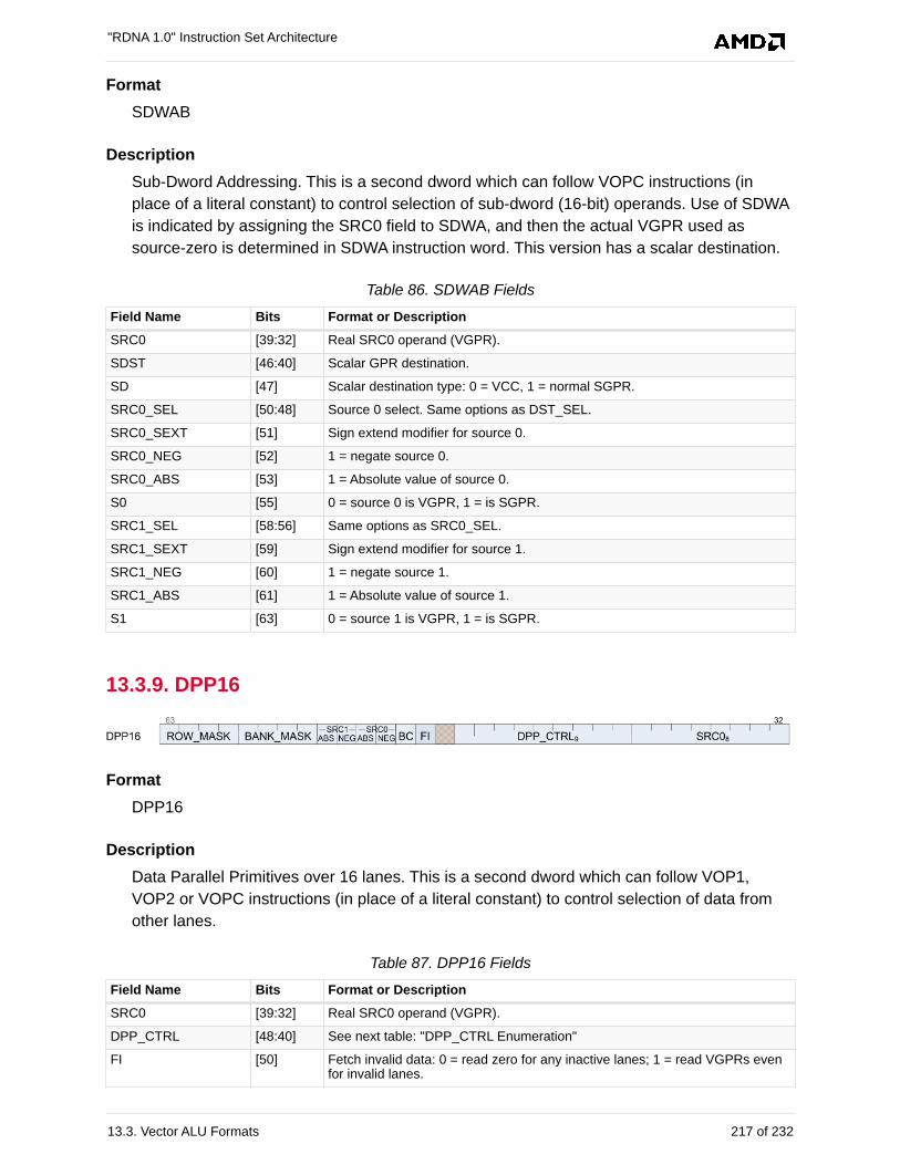
Format
SDWAB
Description
Sub-Dword Addressing. This is a second dword which can follow VOPC instructions (in
place of a literal constant) to control selection of sub-dword (16-bit) operands. Use of SDWA
is indicated by assigning the SRC0 field to SDWA, and then the actual VGPR used as
source-zero is determined in SDWA instruction word. This version has a scalar destination.
Table 86. SDWAB Fields
Field Name Bits Format or Description
SRC0 [39:32] Real SRC0 operand (VGPR).
SDST [46:40] Scalar GPR destination.
SD [47] Scalar destination type: 0 = VCC, 1 = normal SGPR.
SRC0_SEL [50:48] Source 0 select. Same options as DST_SEL.
SRC0_SEXT [51] Sign extend modifier for source 0.
SRC0_NEG [52] 1 = negate source 0.
SRC0_ABS [53] 1 = Absolute value of source 0.
S0 [55] 0 = source 0 is VGPR, 1 = is SGPR.
SRC1_SEL [58:56] Same options as SRC0_SEL.
SRC1_SEXT [59] Sign extend modifier for source 1.
SRC1_NEG [60] 1 = negate source 1.
SRC1_ABS [61] 1 = Absolute value of source 1.
S1 [63] 0 = source 1 is VGPR, 1 = is SGPR.
13.3.9. DPP16
Format
DPP16
Description
Data Parallel Primitives over 16 lanes. This is a second dword which can follow VOP1,
VOP2 or VOPC instructions (in place of a literal constant) to control selection of data from
other lanes.
Table 87. DPP16 Fields
Field Name Bits Format or Description
SRC0 [39:32] Real SRC0 operand (VGPR).
DPP_CTRL [48:40] See next table: "DPP_CTRL Enumeration"
FI [50] Fetch invalid data: 0 = read zero for any inactive lanes; 1 = read VGPRs evenfor invalid lanes.
"RDNA 1.0" Instruction Set Architecture
13.3. Vector ALU Formats 217 of 232
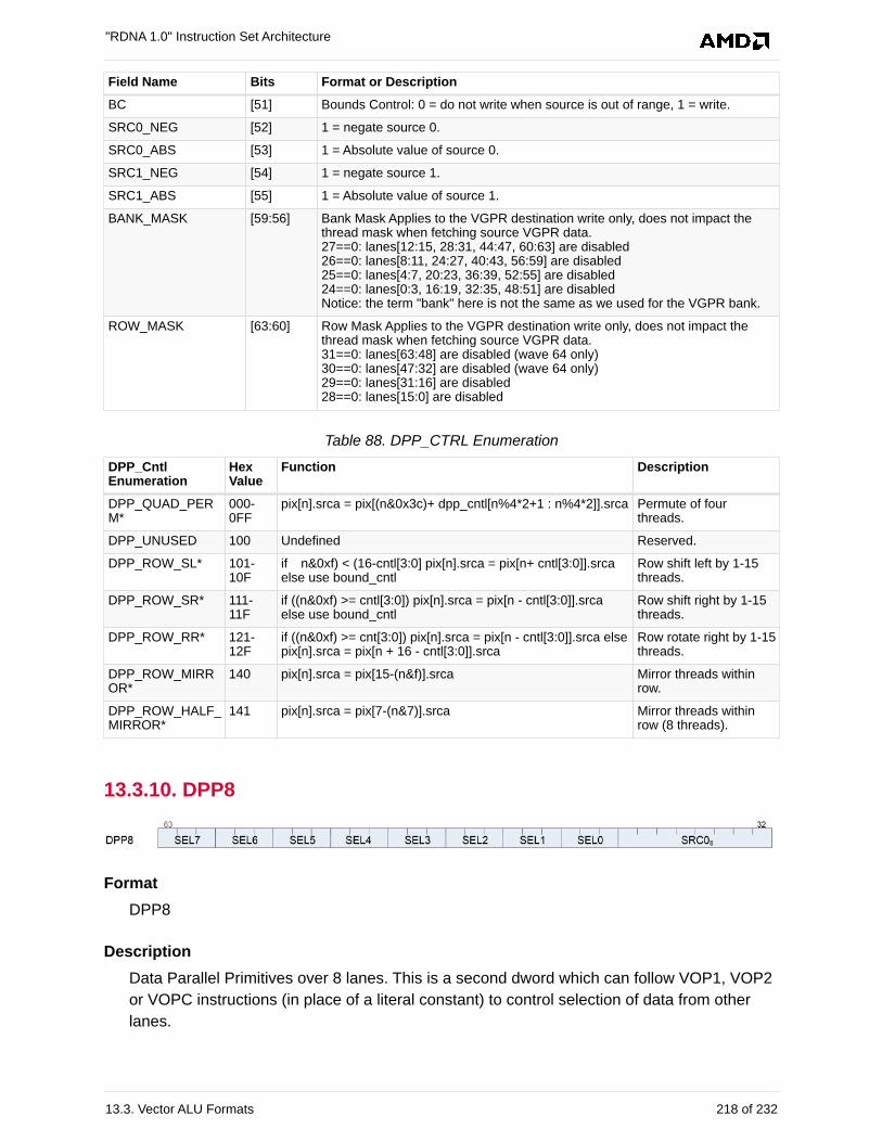
Field Name Bits Format or Description
BC [51] Bounds Control: 0 = do not write when source is out of range, 1 = write.
SRC0_NEG [52] 1 = negate source 0.
SRC0_ABS [53] 1 = Absolute value of source 0.
SRC1_NEG [54] 1 = negate source 1.
SRC1_ABS [55] 1 = Absolute value of source 1.
BANK_MASK [59:56] Bank Mask Applies to the VGPR destination write only, does not impact thethread mask when fetching source VGPR data.27==0: lanes[12:15, 28:31, 44:47, 60:63] are disabled26==0: lanes[8:11, 24:27, 40:43, 56:59] are disabled25==0: lanes[4:7, 20:23, 36:39, 52:55] are disabled24==0: lanes[0:3, 16:19, 32:35, 48:51] are disabledNotice: the term "bank" here is not the same as we used for the VGPR bank.
ROW_MASK [63:60] Row Mask Applies to the VGPR destination write only, does not impact thethread mask when fetching source VGPR data.31==0: lanes[63:48] are disabled (wave 64 only)30==0: lanes[47:32] are disabled (wave 64 only)29==0: lanes[31:16] are disabled28==0: lanes[15:0] are disabled
Table 88. DPP_CTRL Enumeration
DPP_CntlEnumeration
HexValue
Function Description
DPP_QUAD_PERM*
000-0FF
pix[n].srca = pix[(n&0x3c)+ dpp_cntl[n%4*2+1 : n%4*2]].srca Permute of fourthreads.
DPP_UNUSED 100 Undefined Reserved.
DPP_ROW_SL* 101-10F
if n&0xf) < (16-cntl[3:0] pix[n].srca = pix[n+ cntl[3:0]].srcaelse use bound_cntl
Row shift left by 1-15threads.
DPP_ROW_SR* 111-11F
if ((n&0xf) >= cntl[3:0]) pix[n].srca = pix[n - cntl[3:0]].srcaelse use bound_cntl
Row shift right by 1-15threads.
DPP_ROW_RR* 121-12F
if ((n&0xf) >= cnt[3:0]) pix[n].srca = pix[n - cntl[3:0]].srca elsepix[n].srca = pix[n + 16 - cntl[3:0]].srca
Row rotate right by 1-15threads.
DPP_ROW_MIRROR*
140 pix[n].srca = pix[15-(n&f)].srca Mirror threads withinrow.
DPP_ROW_HALF_MIRROR*
141 pix[n].srca = pix[7-(n&7)].srca Mirror threads withinrow (8 threads).
13.3.10. DPP8
Format
DPP8
Description
Data Parallel Primitives over 8 lanes. This is a second dword which can follow VOP1, VOP2
or VOPC instructions (in place of a literal constant) to control selection of data from other
lanes.
"RDNA 1.0" Instruction Set Architecture
13.3. Vector ALU Formats 218 of 232
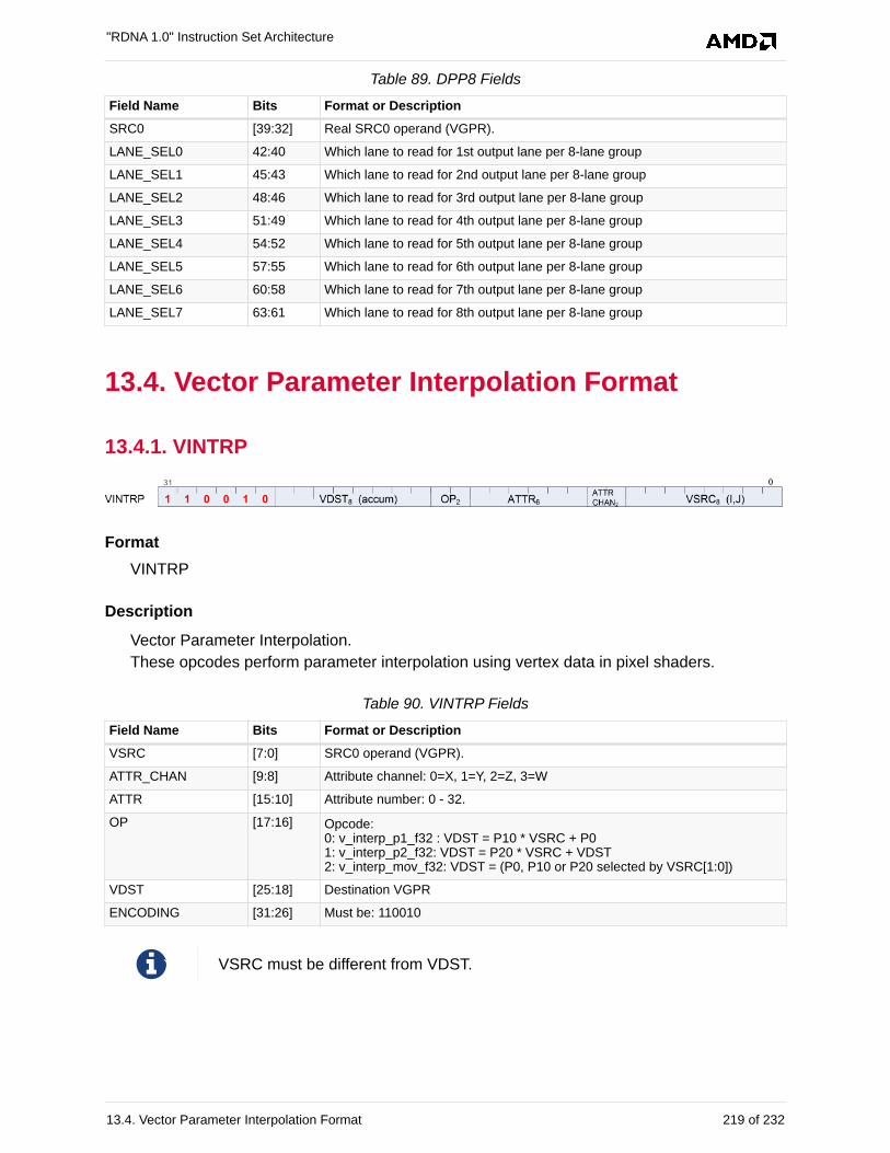
Table 89. DPP8 Fields
Field Name Bits Format or Description
SRC0 [39:32] Real SRC0 operand (VGPR).
LANE_SEL0 42:40 Which lane to read for 1st output lane per 8-lane group
LANE_SEL1 45:43 Which lane to read for 2nd output lane per 8-lane group
LANE_SEL2 48:46 Which lane to read for 3rd output lane per 8-lane group
LANE_SEL3 51:49 Which lane to read for 4th output lane per 8-lane group
LANE_SEL4 54:52 Which lane to read for 5th output lane per 8-lane group
LANE_SEL5 57:55 Which lane to read for 6th output lane per 8-lane group
LANE_SEL6 60:58 Which lane to read for 7th output lane per 8-lane group
LANE_SEL7 63:61 Which lane to read for 8th output lane per 8-lane group
13.4. Vector Parameter Interpolation Format
13.4.1. VINTRP
Format
VINTRP
Description
Vector Parameter Interpolation.
These opcodes perform parameter interpolation using vertex data in pixel shaders.
Table 90. VINTRP Fields
Field Name Bits Format or Description
VSRC [7:0] SRC0 operand (VGPR).
ATTR_CHAN [9:8] Attribute channel: 0=X, 1=Y, 2=Z, 3=W
ATTR [15:10] Attribute number: 0 - 32.
OP [17:16] Opcode:0: v_interp_p1_f32 : VDST = P10 * VSRC + P01: v_interp_p2_f32: VDST = P20 * VSRC + VDST2: v_interp_mov_f32: VDST = (P0, P10 or P20 selected by VSRC[1:0])
VDST [25:18] Destination VGPR
ENCODING [31:26] Must be: 110010
VSRC must be different from VDST.
"RDNA 1.0" Instruction Set Architecture
13.4. Vector Parameter Interpolation Format 219 of 232
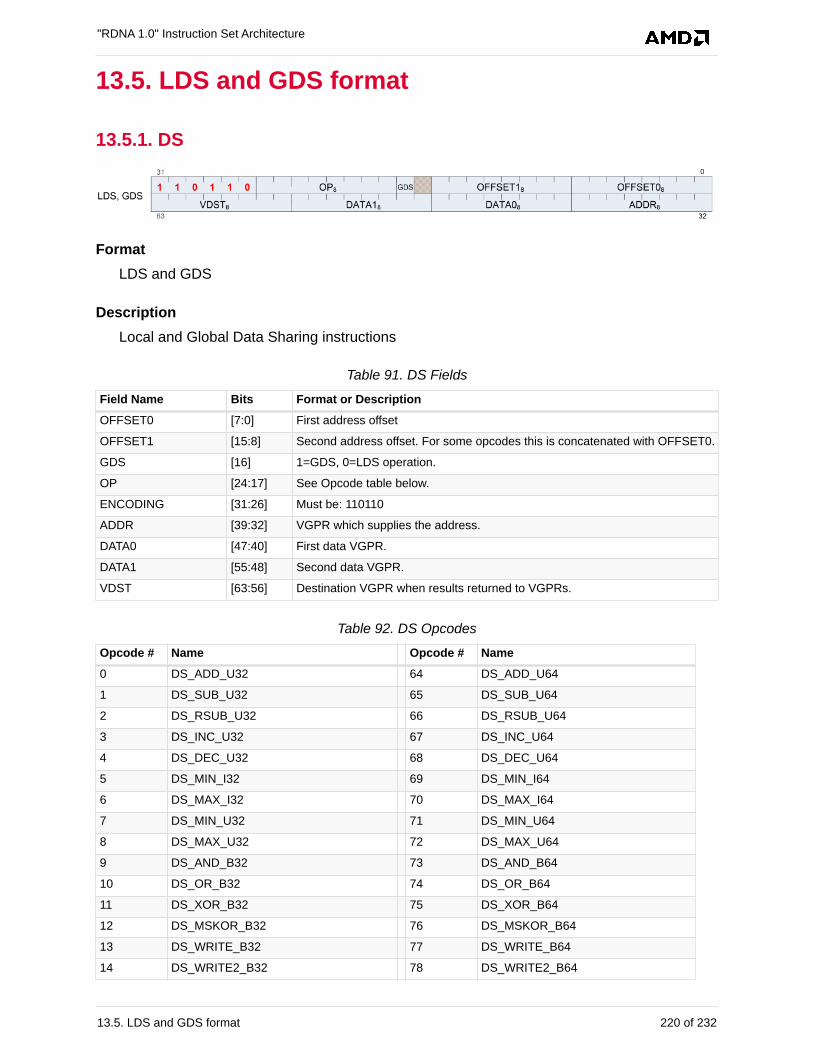
13.5. LDS and GDS format
13.5.1. DS
Format
LDS and GDS
Description
Local and Global Data Sharing instructions
Table 91. DS Fields
Field Name Bits Format or Description
OFFSET0 [7:0] First address offset
OFFSET1 [15:8] Second address offset. For some opcodes this is concatenated with OFFSET0.
GDS [16] 1=GDS, 0=LDS operation.
OP [24:17] See Opcode table below.
ENCODING [31:26] Must be: 110110
ADDR [39:32] VGPR which supplies the address.
DATA0 [47:40] First data VGPR.
DATA1 [55:48] Second data VGPR.
VDST [63:56] Destination VGPR when results returned to VGPRs.
Table 92. DS Opcodes
Opcode # Name Opcode # Name
0 DS_ADD_U32 64 DS_ADD_U64
1 DS_SUB_U32 65 DS_SUB_U64
2 DS_RSUB_U32 66 DS_RSUB_U64
3 DS_INC_U32 67 DS_INC_U64
4 DS_DEC_U32 68 DS_DEC_U64
5 DS_MIN_I32 69 DS_MIN_I64
6 DS_MAX_I32 70 DS_MAX_I64
7 DS_MIN_U32 71 DS_MIN_U64
8 DS_MAX_U32 72 DS_MAX_U64
9 DS_AND_B32 73 DS_AND_B64
10 DS_OR_B32 74 DS_OR_B64
11 DS_XOR_B32 75 DS_XOR_B64
12 DS_MSKOR_B32 76 DS_MSKOR_B64
13 DS_WRITE_B32 77 DS_WRITE_B64
14 DS_WRITE2_B32 78 DS_WRITE2_B64
"RDNA 1.0" Instruction Set Architecture
13.5. LDS and GDS format 220 of 232
Opcode # Name Opcode # Name
15 DS_WRITE2ST64_B32 79 DS_WRITE2ST64_B64
16 DS_CMPST_B32 80 DS_CMPST_B64
17 DS_CMPST_F32 81 DS_CMPST_F64
18 DS_MIN_F32 82 DS_MIN_F64
19 DS_MAX_F32 83 DS_MAX_F64
20 DS_NOP 85 DS_ADD_RTN_F32
21 DS_ADD_F32 96 DS_ADD_RTN_U64
24 DS_GWS_SEMA_RELEASE_ALL 97 DS_SUB_RTN_U64
25 DS_GWS_INIT 98 DS_RSUB_RTN_U64
26 DS_GWS_SEMA_V 99 DS_INC_RTN_U64
27 DS_GWS_SEMA_BR 100 DS_DEC_RTN_U64
28 DS_GWS_SEMA_P 101 DS_MIN_RTN_I64
29 DS_GWS_BARRIER 102 DS_MAX_RTN_I64
30 DS_WRITE_B8 103 DS_MIN_RTN_U64
31 DS_WRITE_B16 104 DS_MAX_RTN_U64
32 DS_ADD_RTN_U32 105 DS_AND_RTN_B64
33 DS_SUB_RTN_U32 106 DS_OR_RTN_B64
34 DS_RSUB_RTN_U32 107 DS_XOR_RTN_B64
35 DS_INC_RTN_U32 108 DS_MSKOR_RTN_B64
36 DS_DEC_RTN_U32 109 DS_WRXCHG_RTN_B64
37 DS_MIN_RTN_I32 110 DS_WRXCHG2_RTN_B64
38 DS_MAX_RTN_I32 111 DS_WRXCHG2ST64_RTN_B64
39 DS_MIN_RTN_U32 112 DS_CMPST_RTN_B64
40 DS_MAX_RTN_U32 113 DS_CMPST_RTN_F64
41 DS_AND_RTN_B32 114 DS_MIN_RTN_F64
42 DS_OR_RTN_B32 115 DS_MAX_RTN_F64
43 DS_XOR_RTN_B32 118 DS_READ_B64
44 DS_MSKOR_RTN_B32 119 DS_READ2_B64
45 DS_WRXCHG_RTN_B32 120 DS_READ2ST64_B64
46 DS_WRXCHG2_RTN_B32 126 DS_CONDXCHG32_RTN_B64
47 DS_WRXCHG2ST64_RTN_B32 160 DS_WRITE_B8_D16_HI
48 DS_CMPST_RTN_B32 161 DS_WRITE_B16_D16_HI
49 DS_CMPST_RTN_F32 162 DS_READ_U8_D16
50 DS_MIN_RTN_F32 163 DS_READ_U8_D16_HI
51 DS_MAX_RTN_F32 164 DS_READ_I8_D16
52 DS_WRAP_RTN_B32 165 DS_READ_I8_D16_HI
53 DS_SWIZZLE_B32 166 DS_READ_U16_D16
54 DS_READ_B32 167 DS_READ_U16_D16_HI
55 DS_READ2_B32 176 DS_WRITE_ADDTID_B32
56 DS_READ2ST64_B32 177 DS_READ_ADDTID_B32
57 DS_READ_I8 178 DS_PERMUTE_B32
58 DS_READ_U8 179 DS_BPERMUTE_B32
"RDNA 1.0" Instruction Set Architecture
13.5. LDS and GDS format 221 of 232
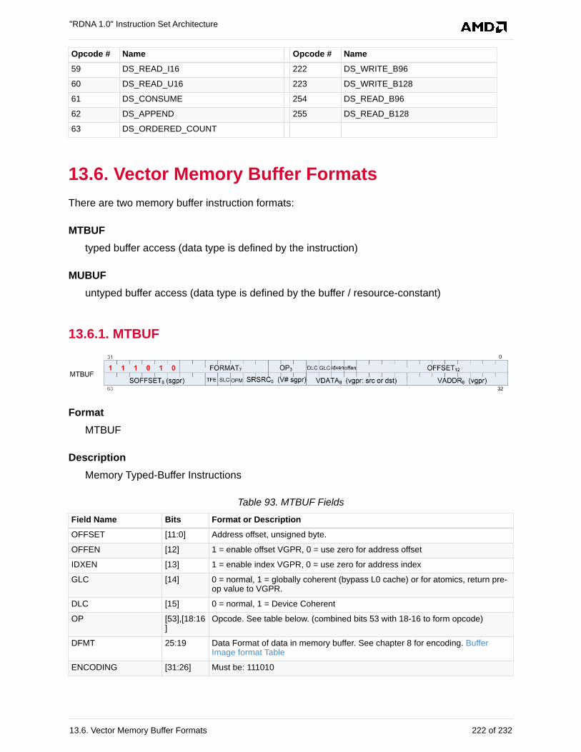
Opcode # Name Opcode # Name
59 DS_READ_I16 222 DS_WRITE_B96
60 DS_READ_U16 223 DS_WRITE_B128
61 DS_CONSUME 254 DS_READ_B96
62 DS_APPEND 255 DS_READ_B128
63 DS_ORDERED_COUNT
13.6. Vector Memory Buffer Formats
There are two memory buffer instruction formats:
MTBUF
typed buffer access (data type is defined by the instruction)
MUBUF
untyped buffer access (data type is defined by the buffer / resource-constant)
13.6.1. MTBUF
Format
MTBUF
Description
Memory Typed-Buffer Instructions
Table 93. MTBUF Fields
Field Name Bits Format or Description
OFFSET [11:0] Address offset, unsigned byte.
OFFEN [12] 1 = enable offset VGPR, 0 = use zero for address offset
IDXEN [13] 1 = enable index VGPR, 0 = use zero for address index
GLC [14] 0 = normal, 1 = globally coherent (bypass L0 cache) or for atomics, return pre-op value to VGPR.
DLC [15] 0 = normal, 1 = Device Coherent
OP [53],[18:16]
Opcode. See table below. (combined bits 53 with 18-16 to form opcode)
DFMT 25:19 Data Format of data in memory buffer. See chapter 8 for encoding. BufferImage format Table
ENCODING [31:26] Must be: 111010
"RDNA 1.0" Instruction Set Architecture
13.6. Vector Memory Buffer Formats 222 of 232
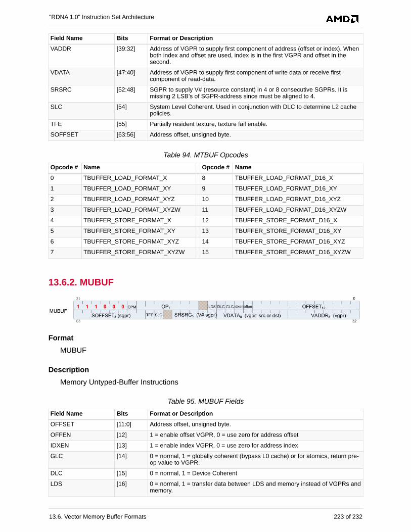
Field Name Bits Format or Description
VADDR [39:32] Address of VGPR to supply first component of address (offset or index). Whenboth index and offset are used, index is in the first VGPR and offset in thesecond.
VDATA [47:40] Address of VGPR to supply first component of write data or receive firstcomponent of read-data.
SRSRC [52:48] SGPR to supply V# (resource constant) in 4 or 8 consecutive SGPRs. It ismissing 2 LSB’s of SGPR-address since must be aligned to 4.
SLC [54] System Level Coherent. Used in conjunction with DLC to determine L2 cachepolicies.
TFE [55] Partially resident texture, texture fail enable.
SOFFSET [63:56] Address offset, unsigned byte.
Table 94. MTBUF Opcodes
Opcode # Name Opcode # Name
0 TBUFFER_LOAD_FORMAT_X 8 TBUFFER_LOAD_FORMAT_D16_X
1 TBUFFER_LOAD_FORMAT_XY 9 TBUFFER_LOAD_FORMAT_D16_XY
2 TBUFFER_LOAD_FORMAT_XYZ 10 TBUFFER_LOAD_FORMAT_D16_XYZ
3 TBUFFER_LOAD_FORMAT_XYZW 11 TBUFFER_LOAD_FORMAT_D16_XYZW
4 TBUFFER_STORE_FORMAT_X 12 TBUFFER_STORE_FORMAT_D16_X
5 TBUFFER_STORE_FORMAT_XY 13 TBUFFER_STORE_FORMAT_D16_XY
6 TBUFFER_STORE_FORMAT_XYZ 14 TBUFFER_STORE_FORMAT_D16_XYZ
7 TBUFFER_STORE_FORMAT_XYZW 15 TBUFFER_STORE_FORMAT_D16_XYZW
13.6.2. MUBUF
Format
MUBUF
Description
Memory Untyped-Buffer Instructions
Table 95. MUBUF Fields
Field Name Bits Format or Description
OFFSET [11:0] Address offset, unsigned byte.
OFFEN [12] 1 = enable offset VGPR, 0 = use zero for address offset
IDXEN [13] 1 = enable index VGPR, 0 = use zero for address index
GLC [14] 0 = normal, 1 = globally coherent (bypass L0 cache) or for atomics, return pre-op value to VGPR.
DLC [15] 0 = normal, 1 = Device Coherent
LDS [16] 0 = normal, 1 = transfer data between LDS and memory instead of VGPRs andmemory.
"RDNA 1.0" Instruction Set Architecture
13.6. Vector Memory Buffer Formats 223 of 232
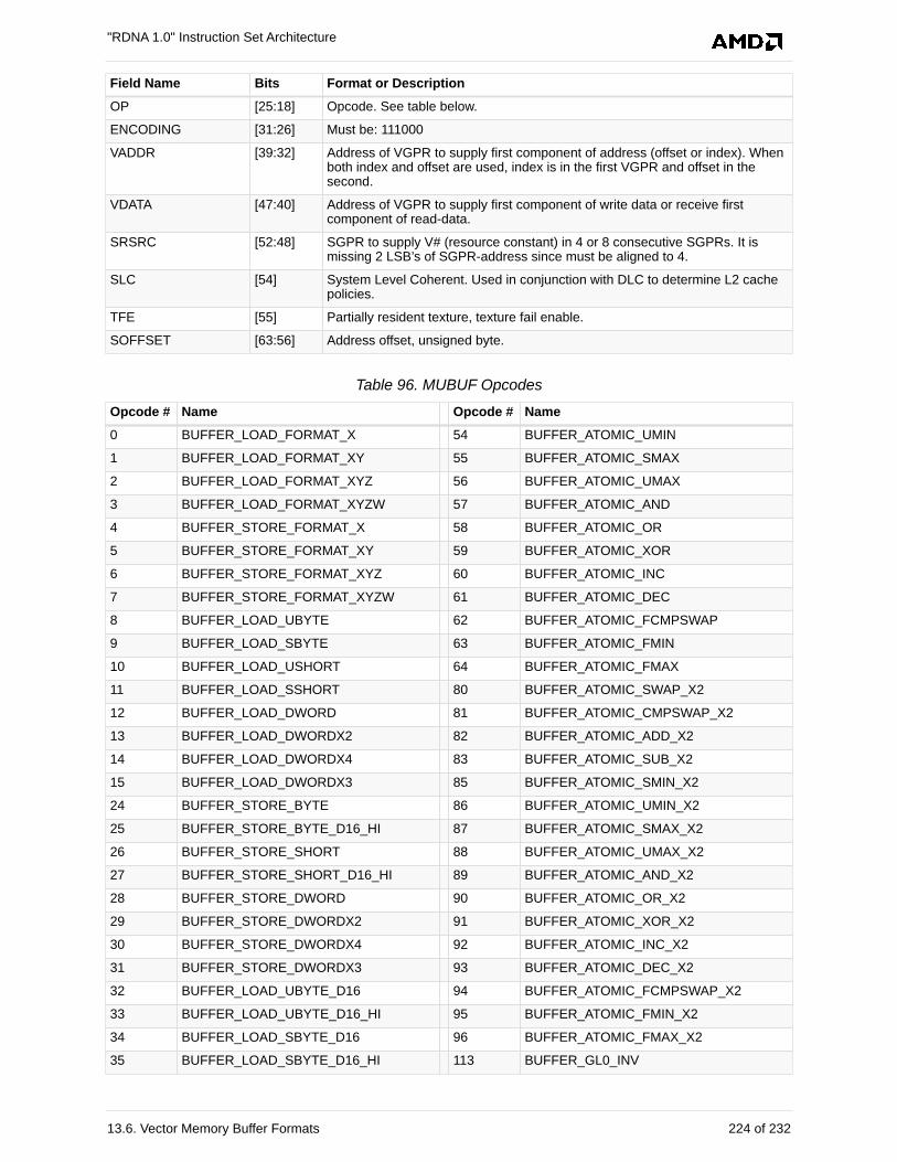
Field Name Bits Format or Description
OP [25:18] Opcode. See table below.
ENCODING [31:26] Must be: 111000
VADDR [39:32] Address of VGPR to supply first component of address (offset or index). Whenboth index and offset are used, index is in the first VGPR and offset in thesecond.
VDATA [47:40] Address of VGPR to supply first component of write data or receive firstcomponent of read-data.
SRSRC [52:48] SGPR to supply V# (resource constant) in 4 or 8 consecutive SGPRs. It ismissing 2 LSB’s of SGPR-address since must be aligned to 4.
SLC [54] System Level Coherent. Used in conjunction with DLC to determine L2 cachepolicies.
TFE [55] Partially resident texture, texture fail enable.
SOFFSET [63:56] Address offset, unsigned byte.
Table 96. MUBUF Opcodes
Opcode # Name Opcode # Name
0 BUFFER_LOAD_FORMAT_X 54 BUFFER_ATOMIC_UMIN
1 BUFFER_LOAD_FORMAT_XY 55 BUFFER_ATOMIC_SMAX
2 BUFFER_LOAD_FORMAT_XYZ 56 BUFFER_ATOMIC_UMAX
3 BUFFER_LOAD_FORMAT_XYZW 57 BUFFER_ATOMIC_AND
4 BUFFER_STORE_FORMAT_X 58 BUFFER_ATOMIC_OR
5 BUFFER_STORE_FORMAT_XY 59 BUFFER_ATOMIC_XOR
6 BUFFER_STORE_FORMAT_XYZ 60 BUFFER_ATOMIC_INC
7 BUFFER_STORE_FORMAT_XYZW 61 BUFFER_ATOMIC_DEC
8 BUFFER_LOAD_UBYTE 62 BUFFER_ATOMIC_FCMPSWAP
9 BUFFER_LOAD_SBYTE 63 BUFFER_ATOMIC_FMIN
10 BUFFER_LOAD_USHORT 64 BUFFER_ATOMIC_FMAX
11 BUFFER_LOAD_SSHORT 80 BUFFER_ATOMIC_SWAP_X2
12 BUFFER_LOAD_DWORD 81 BUFFER_ATOMIC_CMPSWAP_X2
13 BUFFER_LOAD_DWORDX2 82 BUFFER_ATOMIC_ADD_X2
14 BUFFER_LOAD_DWORDX4 83 BUFFER_ATOMIC_SUB_X2
15 BUFFER_LOAD_DWORDX3 85 BUFFER_ATOMIC_SMIN_X2
24 BUFFER_STORE_BYTE 86 BUFFER_ATOMIC_UMIN_X2
25 BUFFER_STORE_BYTE_D16_HI 87 BUFFER_ATOMIC_SMAX_X2
26 BUFFER_STORE_SHORT 88 BUFFER_ATOMIC_UMAX_X2
27 BUFFER_STORE_SHORT_D16_HI 89 BUFFER_ATOMIC_AND_X2
28 BUFFER_STORE_DWORD 90 BUFFER_ATOMIC_OR_X2
29 BUFFER_STORE_DWORDX2 91 BUFFER_ATOMIC_XOR_X2
30 BUFFER_STORE_DWORDX4 92 BUFFER_ATOMIC_INC_X2
31 BUFFER_STORE_DWORDX3 93 BUFFER_ATOMIC_DEC_X2
32 BUFFER_LOAD_UBYTE_D16 94 BUFFER_ATOMIC_FCMPSWAP_X2
33 BUFFER_LOAD_UBYTE_D16_HI 95 BUFFER_ATOMIC_FMIN_X2
34 BUFFER_LOAD_SBYTE_D16 96 BUFFER_ATOMIC_FMAX_X2
35 BUFFER_LOAD_SBYTE_D16_HI 113 BUFFER_GL0_INV
"RDNA 1.0" Instruction Set Architecture
13.6. Vector Memory Buffer Formats 224 of 232
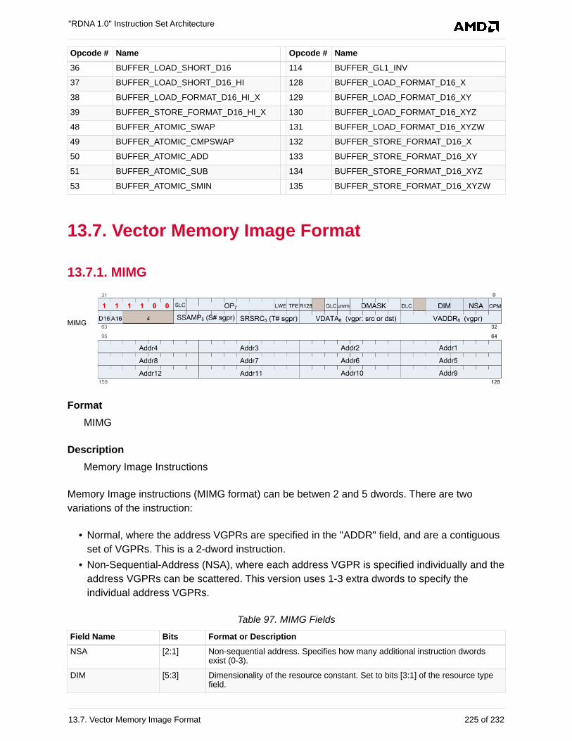
Opcode # Name Opcode # Name
36 BUFFER_LOAD_SHORT_D16 114 BUFFER_GL1_INV
37 BUFFER_LOAD_SHORT_D16_HI 128 BUFFER_LOAD_FORMAT_D16_X
38 BUFFER_LOAD_FORMAT_D16_HI_X 129 BUFFER_LOAD_FORMAT_D16_XY
39 BUFFER_STORE_FORMAT_D16_HI_X 130 BUFFER_LOAD_FORMAT_D16_XYZ
48 BUFFER_ATOMIC_SWAP 131 BUFFER_LOAD_FORMAT_D16_XYZW
49 BUFFER_ATOMIC_CMPSWAP 132 BUFFER_STORE_FORMAT_D16_X
50 BUFFER_ATOMIC_ADD 133 BUFFER_STORE_FORMAT_D16_XY
51 BUFFER_ATOMIC_SUB 134 BUFFER_STORE_FORMAT_D16_XYZ
53 BUFFER_ATOMIC_SMIN 135 BUFFER_STORE_FORMAT_D16_XYZW
13.7. Vector Memory Image Format
13.7.1. MIMG
Format
MIMG
Description
Memory Image Instructions
Memory Image instructions (MIMG format) can be betwen 2 and 5 dwords. There are two
variations of the instruction:
• Normal, where the address VGPRs are specified in the "ADDR" field, and are a contiguous
set of VGPRs. This is a 2-dword instruction.
• Non-Sequential-Address (NSA), where each address VGPR is specified individually and the
address VGPRs can be scattered. This version uses 1-3 extra dwords to specify the
individual address VGPRs.
Table 97. MIMG Fields
Field Name Bits Format or Description
NSA [2:1] Non-sequential address. Specifies how many additional instruction dwordsexist (0-3).
DIM [5:3] Dimensionality of the resource constant. Set to bits [3:1] of the resource typefield.
"RDNA 1.0" Instruction Set Architecture
13.7. Vector Memory Image Format 225 of 232
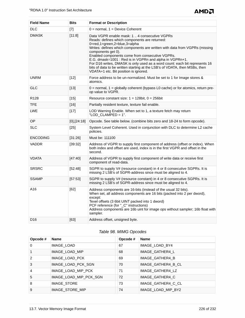
Field Name Bits Format or Description
DLC [7] 0 = normal, 1 = Device Coherent
DMASK [11:8] Data VGPR enable mask: 1 .. 4 consecutive VGPRsReads: defines which components are returned: 0=red,1=green,2=blue,3=alphaWrites: defines which components are written with data from VGPRs (missingcomponents get 0).Enabled components come from consecutive VGPRs.E.G. dmask=1001 : Red is in VGPRn and alpha in VGPRn+1.For D16 writes, DMASK is only used as a word count: each bit represents 16bits of data to be written starting at the LSB’s of VDATA, then MSBs, thenVDATA+1 etc. Bit position is ignored.
UNRM [12] Force address to be un-normalized. Must be set to 1 for Image stores &atomics.
GLC [13] 0 = normal, 1 = globally coherent (bypass L0 cache) or for atomics, return pre-op value to VGPR.
R128 [15] Resource constant size: 1 = 128bit, 0 = 256bit
TFE [16] Partially resident texture, texture fail enable.
LWE [17] LOD Warning Enable. When set to 1, a texture fetch may return"LOD_CLAMPED = 1".
OP [0],[24:18] Opcode. See table below. (combine bits zero and 18-24 to form opcode).
SLC [25] System Level Coherent. Used in conjunction with DLC to determine L2 cachepolicies.
ENCODING [31:26] Must be: 111100
VADDR [39:32] Address of VGPR to supply first component of address (offset or index). Whenboth index and offset are used, index is in the first VGPR and offset in thesecond.
VDATA [47:40] Address of VGPR to supply first component of write data or receive firstcomponent of read-data.
SRSRC [52:48] SGPR to supply V# (resource constant) in 4 or 8 consecutive SGPRs. It ismissing 2 LSB’s of SGPR-address since must be aligned to 4.
SSAMP [57:53] SGPR to supply V# (resource constant) in 4 or 8 consecutive SGPRs. It ismissing 2 LSB’s of SGPR-address since must be aligned to 4.
A16 [62] Address components are 16-bits (instead of the usual 32 bits). When set, all address components are 16 bits (packed into 2 per dword),except:Texel offsets (3 6bit UINT packed into 1 dword)PCF reference (for "_C" instructions)Address components are 16b uint for image ops without sampler; 16b float withsampler.
D16 [63] Address offset, unsigned byte.
Table 98. MIMG Opcodes
Opcode # Name Opcode # Name
0 IMAGE_LOAD 67 IMAGE_LOAD_BY4
1 IMAGE_LOAD_MIP 68 IMAGE_GATHER4_L
2 IMAGE_LOAD_PCK 69 IMAGE_GATHER4_B
3 IMAGE_LOAD_PCK_SGN 70 IMAGE_GATHER4_B_CL
4 IMAGE_LOAD_MIP_PCK 71 IMAGE_GATHER4_LZ
5 IMAGE_LOAD_MIP_PCK_SGN 72 IMAGE_GATHER4_C
8 IMAGE_STORE 73 IMAGE_GATHER4_C_CL
9 IMAGE_STORE_MIP 74 IMAGE_LOAD_MIP_BY2
"RDNA 1.0" Instruction Set Architecture
13.7. Vector Memory Image Format 226 of 232
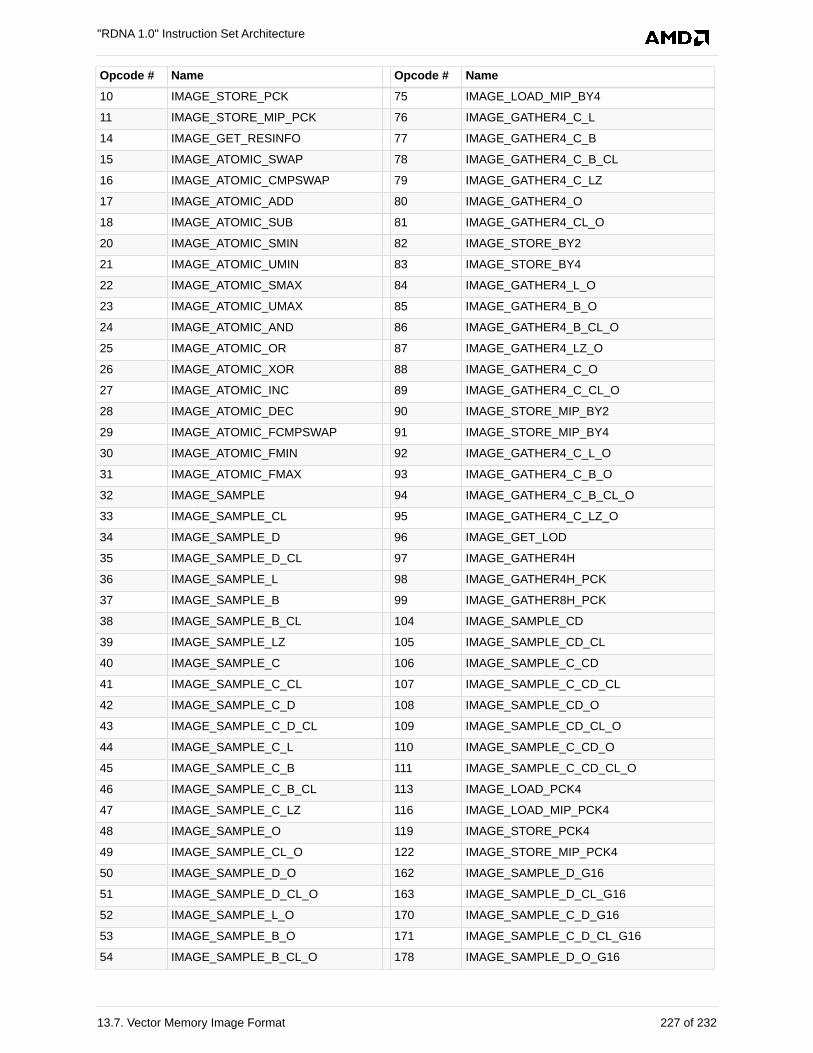
Opcode # Name Opcode # Name
10 IMAGE_STORE_PCK 75 IMAGE_LOAD_MIP_BY4
11 IMAGE_STORE_MIP_PCK 76 IMAGE_GATHER4_C_L
14 IMAGE_GET_RESINFO 77 IMAGE_GATHER4_C_B
15 IMAGE_ATOMIC_SWAP 78 IMAGE_GATHER4_C_B_CL
16 IMAGE_ATOMIC_CMPSWAP 79 IMAGE_GATHER4_C_LZ
17 IMAGE_ATOMIC_ADD 80 IMAGE_GATHER4_O
18 IMAGE_ATOMIC_SUB 81 IMAGE_GATHER4_CL_O
20 IMAGE_ATOMIC_SMIN 82 IMAGE_STORE_BY2
21 IMAGE_ATOMIC_UMIN 83 IMAGE_STORE_BY4
22 IMAGE_ATOMIC_SMAX 84 IMAGE_GATHER4_L_O
23 IMAGE_ATOMIC_UMAX 85 IMAGE_GATHER4_B_O
24 IMAGE_ATOMIC_AND 86 IMAGE_GATHER4_B_CL_O
25 IMAGE_ATOMIC_OR 87 IMAGE_GATHER4_LZ_O
26 IMAGE_ATOMIC_XOR 88 IMAGE_GATHER4_C_O
27 IMAGE_ATOMIC_INC 89 IMAGE_GATHER4_C_CL_O
28 IMAGE_ATOMIC_DEC 90 IMAGE_STORE_MIP_BY2
29 IMAGE_ATOMIC_FCMPSWAP 91 IMAGE_STORE_MIP_BY4
30 IMAGE_ATOMIC_FMIN 92 IMAGE_GATHER4_C_L_O
31 IMAGE_ATOMIC_FMAX 93 IMAGE_GATHER4_C_B_O
32 IMAGE_SAMPLE 94 IMAGE_GATHER4_C_B_CL_O
33 IMAGE_SAMPLE_CL 95 IMAGE_GATHER4_C_LZ_O
34 IMAGE_SAMPLE_D 96 IMAGE_GET_LOD
35 IMAGE_SAMPLE_D_CL 97 IMAGE_GATHER4H
36 IMAGE_SAMPLE_L 98 IMAGE_GATHER4H_PCK
37 IMAGE_SAMPLE_B 99 IMAGE_GATHER8H_PCK
38 IMAGE_SAMPLE_B_CL 104 IMAGE_SAMPLE_CD
39 IMAGE_SAMPLE_LZ 105 IMAGE_SAMPLE_CD_CL
40 IMAGE_SAMPLE_C 106 IMAGE_SAMPLE_C_CD
41 IMAGE_SAMPLE_C_CL 107 IMAGE_SAMPLE_C_CD_CL
42 IMAGE_SAMPLE_C_D 108 IMAGE_SAMPLE_CD_O
43 IMAGE_SAMPLE_C_D_CL 109 IMAGE_SAMPLE_CD_CL_O
44 IMAGE_SAMPLE_C_L 110 IMAGE_SAMPLE_C_CD_O
45 IMAGE_SAMPLE_C_B 111 IMAGE_SAMPLE_C_CD_CL_O
46 IMAGE_SAMPLE_C_B_CL 113 IMAGE_LOAD_PCK4
47 IMAGE_SAMPLE_C_LZ 116 IMAGE_LOAD_MIP_PCK4
48 IMAGE_SAMPLE_O 119 IMAGE_STORE_PCK4
49 IMAGE_SAMPLE_CL_O 122 IMAGE_STORE_MIP_PCK4
50 IMAGE_SAMPLE_D_O 162 IMAGE_SAMPLE_D_G16
51 IMAGE_SAMPLE_D_CL_O 163 IMAGE_SAMPLE_D_CL_G16
52 IMAGE_SAMPLE_L_O 170 IMAGE_SAMPLE_C_D_G16
53 IMAGE_SAMPLE_B_O 171 IMAGE_SAMPLE_C_D_CL_G16
54 IMAGE_SAMPLE_B_CL_O 178 IMAGE_SAMPLE_D_O_G16
"RDNA 1.0" Instruction Set Architecture
13.7. Vector Memory Image Format 227 of 232
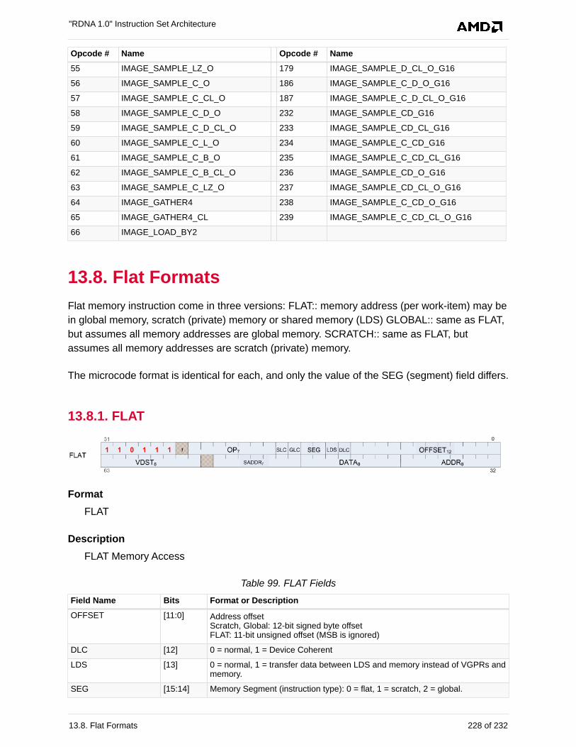
Opcode # Name Opcode # Name
55 IMAGE_SAMPLE_LZ_O 179 IMAGE_SAMPLE_D_CL_O_G16
56 IMAGE_SAMPLE_C_O 186 IMAGE_SAMPLE_C_D_O_G16
57 IMAGE_SAMPLE_C_CL_O 187 IMAGE_SAMPLE_C_D_CL_O_G16
58 IMAGE_SAMPLE_C_D_O 232 IMAGE_SAMPLE_CD_G16
59 IMAGE_SAMPLE_C_D_CL_O 233 IMAGE_SAMPLE_CD_CL_G16
60 IMAGE_SAMPLE_C_L_O 234 IMAGE_SAMPLE_C_CD_G16
61 IMAGE_SAMPLE_C_B_O 235 IMAGE_SAMPLE_C_CD_CL_G16
62 IMAGE_SAMPLE_C_B_CL_O 236 IMAGE_SAMPLE_CD_O_G16
63 IMAGE_SAMPLE_C_LZ_O 237 IMAGE_SAMPLE_CD_CL_O_G16
64 IMAGE_GATHER4 238 IMAGE_SAMPLE_C_CD_O_G16
65 IMAGE_GATHER4_CL 239 IMAGE_SAMPLE_C_CD_CL_O_G16
66 IMAGE_LOAD_BY2
13.8. Flat Formats
Flat memory instruction come in three versions: FLAT:: memory address (per work-item) may be
in global memory, scratch (private) memory or shared memory (LDS) GLOBAL:: same as FLAT,
but assumes all memory addresses are global memory. SCRATCH:: same as FLAT, but
assumes all memory addresses are scratch (private) memory.
The microcode format is identical for each, and only the value of the SEG (segment) field differs.
13.8.1. FLAT
Format
FLAT
Description
FLAT Memory Access
Table 99. FLAT Fields
Field Name Bits Format or Description
OFFSET [11:0] Address offsetScratch, Global: 12-bit signed byte offsetFLAT: 11-bit unsigned offset (MSB is ignored)
DLC [12] 0 = normal, 1 = Device Coherent
LDS [13] 0 = normal, 1 = transfer data between LDS and memory instead of VGPRs andmemory.
SEG [15:14] Memory Segment (instruction type): 0 = flat, 1 = scratch, 2 = global.
"RDNA 1.0" Instruction Set Architecture
13.8. Flat Formats 228 of 232
Field Name Bits Format or Description
GLC [16] 0 = normal, 1 = globally coherent (bypass L0 cache) or for atomics, return pre-op value to VGPR.
SLC [17] System Level Coherent. Used in conjunction with DLC to determine L2 cachepolicies.
OP [24:18] Opcode. See tables below for FLAT, SCRATCH and GLOBAL opcodes.
ENCODING [31:26] Must be: 110111
ADDR [39:32] VGPR which holds address or offset. For 64-bit addresses, ADDR has theLSB’s and ADDR+1 has the MSBs. For offset a single VGPR has a 32 bitunsigned offset.For FLAT_*: specifies an address.For GLOBAL_* and SCRATCH_* when SADDR is 0x7f: specifies an address.For GLOBAL_* and SCRATCH_* when SADDR is not 0x7f: specifies an offset.
DATA [47:40] VGPR which supplies data.
SADDR [54:48] Scalar SGPR which provides an address of offset (unsigned). Set this field to0x7f to disable use.Meaning of this field is different for Scratch and Global:FLAT: Unused Scratch: use an SGPR for the address instead of a VGPRGlobal: use the SGPR to provide a base address and the VGPR provides a 32-bit byte offset.
VDST [63:56] Destination VGPR for data returned from memory to VGPRs.
Table 100. FLAT Opcodes
Opcode # Name Opcode # Name
8 FLAT_LOAD_UBYTE 54 FLAT_ATOMIC_UMIN
9 FLAT_LOAD_SBYTE 55 FLAT_ATOMIC_SMAX
10 FLAT_LOAD_USHORT 56 FLAT_ATOMIC_UMAX
11 FLAT_LOAD_SSHORT 57 FLAT_ATOMIC_AND
12 FLAT_LOAD_DWORD 58 FLAT_ATOMIC_OR
13 FLAT_LOAD_DWORDX2 59 FLAT_ATOMIC_XOR
14 FLAT_LOAD_DWORDX4 60 FLAT_ATOMIC_INC
15 FLAT_LOAD_DWORDX3 61 FLAT_ATOMIC_DEC
24 FLAT_STORE_BYTE 62 FLAT_ATOMIC_FCMPSWAP
25 FLAT_STORE_BYTE_D16_HI 63 FLAT_ATOMIC_FMIN
26 FLAT_STORE_SHORT 64 FLAT_ATOMIC_FMAX
27 FLAT_STORE_SHORT_D16_HI 80 FLAT_ATOMIC_SWAP_X2
28 FLAT_STORE_DWORD 81 FLAT_ATOMIC_CMPSWAP_X2
29 FLAT_STORE_DWORDX2 82 FLAT_ATOMIC_ADD_X2
30 FLAT_STORE_DWORDX4 83 FLAT_ATOMIC_SUB_X2
31 FLAT_STORE_DWORDX3 85 FLAT_ATOMIC_SMIN_X2
32 FLAT_LOAD_UBYTE_D16 86 FLAT_ATOMIC_UMIN_X2
33 FLAT_LOAD_UBYTE_D16_HI 87 FLAT_ATOMIC_SMAX_X2
34 FLAT_LOAD_SBYTE_D16 88 FLAT_ATOMIC_UMAX_X2
35 FLAT_LOAD_SBYTE_D16_HI 89 FLAT_ATOMIC_AND_X2
36 FLAT_LOAD_SHORT_D16 90 FLAT_ATOMIC_OR_X2
37 FLAT_LOAD_SHORT_D16_HI 91 FLAT_ATOMIC_XOR_X2
48 FLAT_ATOMIC_SWAP 92 FLAT_ATOMIC_INC_X2
"RDNA 1.0" Instruction Set Architecture
13.8. Flat Formats 229 of 232
Opcode # Name Opcode # Name
49 FLAT_ATOMIC_CMPSWAP 93 FLAT_ATOMIC_DEC_X2
50 FLAT_ATOMIC_ADD 94 FLAT_ATOMIC_FCMPSWAP_X2
51 FLAT_ATOMIC_SUB 95 FLAT_ATOMIC_FMIN_X2
53 FLAT_ATOMIC_SMIN 96 FLAT_ATOMIC_FMAX_X2
13.8.2. GLOBAL
Table 101. GLOBAL Opcodes
Opcode # Name Opcode # Name
8 GLOBAL_LOAD_UBYTE 54 GLOBAL_ATOMIC_UMIN
9 GLOBAL_LOAD_SBYTE 55 GLOBAL_ATOMIC_SMAX
10 GLOBAL_LOAD_USHORT 56 GLOBAL_ATOMIC_UMAX
11 GLOBAL_LOAD_SSHORT 57 GLOBAL_ATOMIC_AND
12 GLOBAL_LOAD_DWORD 58 GLOBAL_ATOMIC_OR
13 GLOBAL_LOAD_DWORDX2 59 GLOBAL_ATOMIC_XOR
14 GLOBAL_LOAD_DWORDX4 60 GLOBAL_ATOMIC_INC
15 GLOBAL_LOAD_DWORDX3 61 GLOBAL_ATOMIC_DEC
24 GLOBAL_STORE_BYTE 62 GLOBAL_ATOMIC_FCMPSWAP
25 GLOBAL_STORE_BYTE_D16_HI 63 GLOBAL_ATOMIC_FMIN
26 GLOBAL_STORE_SHORT 64 GLOBAL_ATOMIC_FMAX
27 GLOBAL_STORE_SHORT_D16_HI 80 GLOBAL_ATOMIC_SWAP_X2
28 GLOBAL_STORE_DWORD 81 GLOBAL_ATOMIC_CMPSWAP_X2
29 GLOBAL_STORE_DWORDX2 82 GLOBAL_ATOMIC_ADD_X2
30 GLOBAL_STORE_DWORDX4 83 GLOBAL_ATOMIC_SUB_X2
31 GLOBAL_STORE_DWORDX3 85 GLOBAL_ATOMIC_SMIN_X2
32 GLOBAL_LOAD_UBYTE_D16 86 GLOBAL_ATOMIC_UMIN_X2
33 GLOBAL_LOAD_UBYTE_D16_HI 87 GLOBAL_ATOMIC_SMAX_X2
34 GLOBAL_LOAD_SBYTE_D16 88 GLOBAL_ATOMIC_UMAX_X2
35 GLOBAL_LOAD_SBYTE_D16_HI 89 GLOBAL_ATOMIC_AND_X2
36 GLOBAL_LOAD_SHORT_D16 90 GLOBAL_ATOMIC_OR_X2
37 GLOBAL_LOAD_SHORT_D16_HI 91 GLOBAL_ATOMIC_XOR_X2
48 GLOBAL_ATOMIC_SWAP 92 GLOBAL_ATOMIC_INC_X2
49 GLOBAL_ATOMIC_CMPSWAP 93 GLOBAL_ATOMIC_DEC_X2
50 GLOBAL_ATOMIC_ADD 94 GLOBAL_ATOMIC_FCMPSWAP_X2
51 GLOBAL_ATOMIC_SUB 95 GLOBAL_ATOMIC_FMIN_X2
53 GLOBAL_ATOMIC_SMIN 96 GLOBAL_ATOMIC_FMAX_X2
13.8.3. SCRATCH
Table 102. SCRATCH Opcodes
"RDNA 1.0" Instruction Set Architecture
13.8. Flat Formats 230 of 232
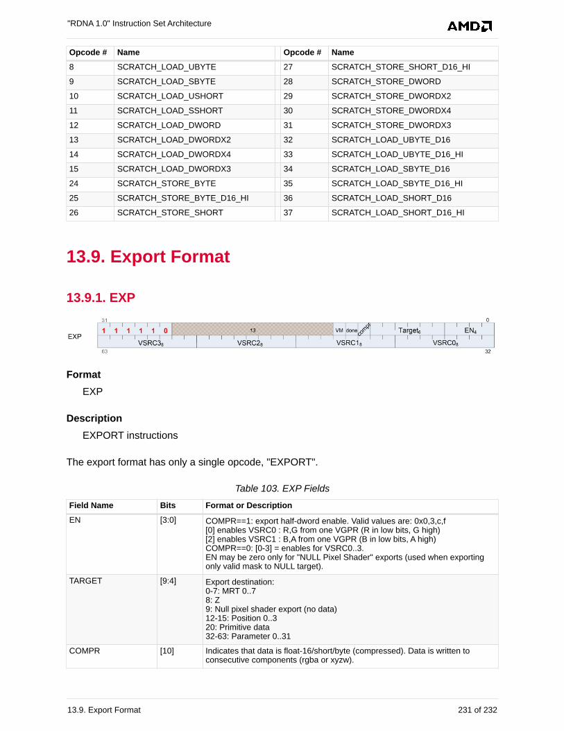
Opcode # Name Opcode # Name
8 SCRATCH_LOAD_UBYTE 27 SCRATCH_STORE_SHORT_D16_HI
9 SCRATCH_LOAD_SBYTE 28 SCRATCH_STORE_DWORD
10 SCRATCH_LOAD_USHORT 29 SCRATCH_STORE_DWORDX2
11 SCRATCH_LOAD_SSHORT 30 SCRATCH_STORE_DWORDX4
12 SCRATCH_LOAD_DWORD 31 SCRATCH_STORE_DWORDX3
13 SCRATCH_LOAD_DWORDX2 32 SCRATCH_LOAD_UBYTE_D16
14 SCRATCH_LOAD_DWORDX4 33 SCRATCH_LOAD_UBYTE_D16_HI
15 SCRATCH_LOAD_DWORDX3 34 SCRATCH_LOAD_SBYTE_D16
24 SCRATCH_STORE_BYTE 35 SCRATCH_LOAD_SBYTE_D16_HI
25 SCRATCH_STORE_BYTE_D16_HI 36 SCRATCH_LOAD_SHORT_D16
26 SCRATCH_STORE_SHORT 37 SCRATCH_LOAD_SHORT_D16_HI
13.9. Export Format
13.9.1. EXP
Format
EXP
Description
EXPORT instructions
The export format has only a single opcode, "EXPORT".
Table 103. EXP Fields
Field Name Bits Format or Description
EN [3:0] COMPR==1: export half-dword enable. Valid values are: 0x0,3,c,f[0] enables VSRC0 : R,G from one VGPR (R in low bits, G high)[2] enables VSRC1 : B,A from one VGPR (B in low bits, A high)COMPR==0: [0-3] = enables for VSRC0..3. EN may be zero only for "NULL Pixel Shader" exports (used when exportingonly valid mask to NULL target).
TARGET [9:4] Export destination:0-7: MRT 0..78: Z9: Null pixel shader export (no data)12-15: Position 0..320: Primitive data32-63: Parameter 0..31
COMPR [10] Indicates that data is float-16/short/byte (compressed). Data is written toconsecutive components (rgba or xyzw).
"RDNA 1.0" Instruction Set Architecture
13.9. Export Format 231 of 232
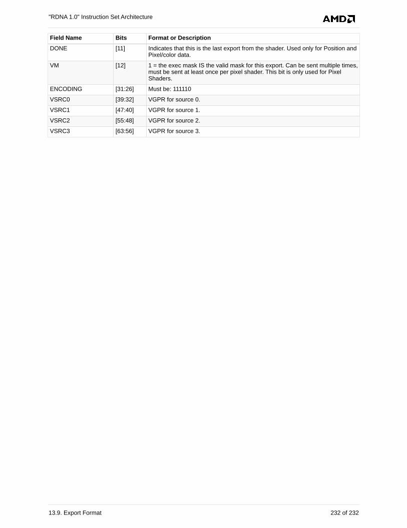
Field Name Bits Format or Description
DONE [11] Indicates that this is the last export from the shader. Used only for Position andPixel/color data.
VM [12] 1 = the exec mask IS the valid mask for this export. Can be sent multiple times,must be sent at least once per pixel shader. This bit is only used for PixelShaders.
ENCODING [31:26] Must be: 111110
VSRC0 [39:32] VGPR for source 0.
VSRC1 [47:40] VGPR for source 1.
VSRC2 [55:48] VGPR for source 2.
VSRC3 [63:56] VGPR for source 3.
"RDNA 1.0" Instruction Set Architecture
13.9. Export Format 232 of 232