real-time high-resolution mid-infrared optical coherence tomography · coherence tomography system...
TRANSCRIPT
General rights Copyright and moral rights for the publications made accessible in the public portal are retained by the authors and/or other copyright owners and it is a condition of accessing publications that users recognise and abide by the legal requirements associated with these rights.
Users may download and print one copy of any publication from the public portal for the purpose of private study or research.
You may not further distribute the material or use it for any profit-making activity or commercial gain
You may freely distribute the URL identifying the publication in the public portal If you believe that this document breaches copyright please contact us providing details, and we will remove access to the work immediately and investigate your claim.
Downloaded from orbit.dtu.dk on: Jul 18, 2020
Real-time high-resolution mid-infrared optical coherence tomography
Israelsen, Niels M.; Petersen, Christian R.; Barh, Ajanta; Jain, Deepak; Jensen, Mikkel; Hannesschläger,Günther; Tidemand-Lichtenberg, Peter; Pedersen, Christian; Podoleanu, Adrian; Bang, Ole
Published in:Light: Science and Applications
Link to article, DOI:10.1038/s41377-019-0122-5
Publication date:2019
Document VersionPublisher's PDF, also known as Version of record
Link back to DTU Orbit
Citation (APA):Israelsen, N. M., Petersen, C. R., Barh, A., Jain, D., Jensen, M., Hannesschläger, G., Tidemand-Lichtenberg, P.,Pedersen, C., Podoleanu, A., & Bang, O. (2019). Real-time high-resolution mid-infrared optical coherencetomography. Light: Science and Applications, 8(1), [11]. https://doi.org/10.1038/s41377-019-0122-5
Israelsen et al. Light: Science & Applications (2019) 8:11 Official journal of the CIOMP 2047-7538https://doi.org/10.1038/s41377-019-0122-5 www.nature.com/lsa
ART ICLE Open Ac ce s s
Real-time high-resolution mid-infraredoptical coherence tomographyNiels M. Israelsen1,2, Christian R. Petersen 1,2, Ajanta Barh1, Deepak Jain1, Mikkel Jensen 1, Günther Hannesschläger3,Peter Tidemand-Lichtenberg1,4, Christian Pedersen1,4, Adrian Podoleanu5 and Ole Bang1,2
AbstractThe potential for improving the penetration depth of optical coherence tomography systems by using light sourceswith longer wavelengths has been known since the inception of the technique in the early 1990s. Nevertheless, thedevelopment of mid-infrared optical coherence tomography has long been challenged by the maturity and fidelity ofoptical components in this spectral region, resulting in slow acquisition, low sensitivity, and poor axial resolution. Inthis work, a mid-infrared spectral-domain optical coherence tomography system operating at a central wavelength of4 µm and an axial resolution of 8.6 µm is demonstrated. The system produces two-dimensional cross-sectional imagesin real time enabled by a high-brightness 0.9- to 4.7-µm mid-infrared supercontinuum source with a pulse repetitionrate of 1 MHz for illumination and broadband upconversion of more than 1-µm bandwidth from 3.58–4.63 µm to820–865 nm, where a standard 800-nm spectrometer can be used for fast detection. The images produced by themid-infrared system are compared with those delivered by a state-of-the-art ultra-high-resolution near-infrared opticalcoherence tomography system operating at 1.3 μm, and the potential applications and samples suited for thistechnology are discussed. In doing so, the first practical mid-infrared optical coherence tomography system isdemonstrated, with immediate applications in real-time non-destructive testing for the inspection of defects andthickness measurements in samples that exhibit strong scattering at shorter wavelengths.
IntroductionOptical coherence tomography (OCT) has been estab-
lished as one of the most successful and significant opticaltechniques for biophotonics and clinical biomedicalimaging, most notably within the field of ophthalmology.OCT has the ability to perform real-time, non-invasive,and noncontact measurements in reflection, providingthree-dimensional (3D) sample visualization1,2. Rapidadvances in light sources, detectors, and components forthe visible and near-infrared (IR) spectral region haveenabled the development of advanced functional techni-ques as well as high-speed, high-resolution in vivo ima-ging3,4, including OCT. In recent years, there has been agrowing interest in applying OCT for non-destructivetesting (NDT) in cultural heritage conservation and
industrial quality control to measure, for example, thethickness of coatings and layered materials and to identifysubsurface structures and defects5–7. In this regard, OCTstands out from other traditional NDT techniques, suchas high-frequency laser ultrasonic (LUS) imaging, ter-ahertz (THz) imaging, and micro X-ray computedtomography (μCT), each with its own advantages anddisadvantages. Specifically, OCT can offer several advan-tages in applications prohibiting the use of μCT due to itslow contrast and hazardous ionizing radiation, LUS due tothe need for noncontact measurements, and THz due topoor spatial resolution and long acquisition time7. Fur-thermore, OCT is an industry-ready technology that isrelatively robust and easy to apply, and can be imple-mented using low optical power8. However, the mainlimitation of OCT is the strong scattering of light atvisible and near-IR wavelengths, which limits the pene-tration depth in turbid media from a few tens to hundredsof microns depending on the sample. Since scattering
© The Author(s) 2019OpenAccessThis article is licensedunder aCreativeCommonsAttribution 4.0 International License,whichpermits use, sharing, adaptation, distribution and reproductionin any medium or format, as long as you give appropriate credit to the original author(s) and the source, provide a link to the Creative Commons license, and indicate if
changesweremade. The images or other third partymaterial in this article are included in the article’s Creative Commons license, unless indicated otherwise in a credit line to thematerial. Ifmaterial is not included in the article’s Creative Commons license and your intended use is not permitted by statutory regulation or exceeds the permitted use, you will need to obtainpermission directly from the copyright holder. To view a copy of this license, visit http://creativecommons.org/licenses/by/4.0/.
Correspondence: Christian R. Petersen ([email protected])1DTU Fotonik, Technical University of Denmark, 2800 Kgs, Lyngby, Denmark2NORBLIS IVS, Virumgade 35 D, Virum 2830, DenmarkFull list of author information is available at the end of the article.
1234
5678
90():,;
1234
5678
90():,;
1234567890():,;
1234
5678
90():,;
losses are inversely proportional to the wavelength of lightrelative to the size of the scattering features, it has longbeen known that the penetration of OCT would benefitfrom employing a longer center wavelength. Currentstate-of-the-art commercially available OCT systems forNDT operate in the 1.3-μm wavelength range, utilizingthe low water absorption and the maturity of optical fibersand components developed for telecommunications inthis region. At longer wavelengths, the light sources anddetectors are significantly less efficient and the compo-nents are less mature. In addition, water absorption isgenerally considered to be too strong for imaging ofbiological tissues and other aqueous samples in thisregion, and even in the absence of water, many materialsmay have significant vibrational absorption bands in thisregion. Therefore, the combined effect of absorption andscattering on the penetration depth makes it nontrivial toassess whether a sample would benefit from being imagedat a longer wavelength. However, limited penetration iseasily confirmed at 1.3 μm, where previous studies on agreat variety of samples have found that scattering is theprimary obstacle for deeper imaging. These studies haveexamined tablet coatings9, various polymer samples, fibercomposite materials6,10, LEDs and printed electronics11,12,and paper quality13, as well as microchannels inceramics14.OCT studies investigating longer wavelengths in the
near-IR regime at 1.7 and 2 µm have been reported, whereincreased penetration was demonstrated in compositepaint samples15,16, intralipids, rubber17,18, and ceramicmaterials such as alumina and zirconia19, although
scattering was still considered to be the dominant factorin limiting penetration.Few attempts have been made to utilize the vast
potential of mid-IR OCT, such as the early proof ofconcept work of Colley et al.20,21 demonstrating the firstin-depth reflectivity profiles. In their work, a singlereflectivity profile (A-scan) of a calcium fluoride windowand a topographic image of a gold-palladium-coated tis-sue sample were presented. These first measurementswere based on quantum cascade laser (QCL) emission andcryogenically cooled mercury cadmium telluride (MCT)detection using a time-domain OCT scheme. With acenter wavelength of 7 µm, Colley et al.20,21 achieved anaxial resolution of 30 µm with an acquisition time of 30min for a single reflectivity profile, which was heavilyaffected by the side lobes due to the heavily modulatedspectral shape. A similar study on mid-IR OCT wasreported by Varnell et al.22 using a superluminescent QCLcentered at 5 µm with a smooth spectral shape, resultingin an improved signal-to-noise ratio (SNR) but a reducedbandwidth, leading to a poor axial resolution of 50 µm.Recently, Paterova et al.23 investigated tunable mid-IROCT up to 3 µm using visible light detection by exploitingthe nonlinear interference of correlated photon pairsgenerated through spontaneous parametric down-conversion. However, due to the narrow bandwidth oftheir tunable source, the axial resolution at 3-µm centerwavelength was limited to 93 µm, while the time-domainOCT scheme chosen limited the sensitivity and acquisi-tion speed. In this work, a real-time mid-IR OCT systemwith a high axial resolution of 8.6 µm is demonstrated.
Upconversion
CMOS spectrometerFluoride fiber
MOPA laser
Scanner
X
Y
Interferometer
1.5–2.7 μm
0.9–4.7 μm
3.58–4.63 μm → 820–865 nm
Fig. 1 Overview of the 4-μm OCT system. The OCT system consists of five parts that are connected via optical fiber: a broadband mid-IR SC sourcebased on a MOPA pump laser and fluoride fiber, a free-space Michelson interferometer, a scanning x,y translation stage, a frequency upconversionmodule, and a silicon CMOS-based spectrometer. See Methods section for a detailed description of the setup. OCT optical coherence tomography, IRinfrared, SC supercontinuum, MOPA master-oscillator power amplifier, CMOS complementary metal–oxide–semiconductor
Israelsen et al. Light: Science & Applications (2019) 8:11 Page 2 of 13
This is achieved by the use of a broadband, high-brightness mid-IR supercontinuum (SC) source for illu-mination and a broadband frequency upconversion sys-tem for detection. Using this technique, an improvedpenetration of the 4-µm OCT system compared to a 1.3-µm OCT system is demonstrated for the same opticalpower. The 1.3-µm OCT system used for comparison is astate-of-the-art spectral-domain system using a near-IRSC source with a 400-nm bandwidth (for details,see Supplementary materials), which was recently used ina clinical skin study24.
ResultsCharacterization of the 4-µm OCT systemAn overview of the system is shown in Fig. 1 (see
Methods for details). The system consists of five modularparts: a custom mid-IR SC source based on a 1.55-μmmaster-oscillator power amplifier (MOPA) pump laserand a single-mode zirconium fluoride fiber, a Michelsoninterferometer, a scanning sample translation system, anin-house developed frequency upconversion module, anda silicon complementary metal–oxide–semiconductor(CMOS)-based spectrometer. Each subsystem is con-nected via optical fiber to ease the coupling and alignmentbetween subsystems. The mid-IR SC source produces acontinuous spectrum from 0.9 to 4.7 μm and is set tooperate at 1MHz pulse repetition rate generating 40 mWof average power above 3.5 μm, which is comparable inbrightness to synchrotron radiation25. The spectral com-ponents below 3.5 μm are blocked by a longpass filter,resulting in 20mW coupled to the sample arm of theinterferometer. The beam is focused onto the sampleusing a barium fluoride (BaF2) lens, and images areacquired by moving the sample using motorized transla-tion stages. The sample and reference signals are collectedin a single-mode indium fluoride fiber and relayed to theupconversion module for spectral conversion to the near-IR. The upconverted signal is then coupled to a multi-mode silica fiber and imaged onto the spectrometer toresolve the spectrum. Examples of the spectra before andafter upconversion are shown in Fig. 2a.Here, the key technology for enabling fast and low-noise
detection is the broadband nonlinear frequency upcon-version. Shifting the spectrum to the near-IR is critical tothe performance of the system, since state-of-the-art mid-IR detectors (e.g., PbSe, InSb, MCT) suffer from intrinsicthermal background noise and low responsivity comparedto their near-IR counterparts. Furthermore, due to therelative immaturity and high cost of mid-IR detectors,focal plane arrays and array spectrometers usually have alimited number of pixels available for detection, thusreducing the spectral resolution that minimizes the axialrange. To alleviate these shortcomings, researchers havedemonstrated frequency upconversion-based detectors
that are functional at room temperature as a promisingalternative to traditional direct detection schemes26. Inthis process, the mid-IR signal passes through a suitablenonlinear crystal, where it mixes with a strong mixingfield; thus, a near-IR sum frequency signal is generatedwithout any loss of the information encoded in thespectral modulation of the mid-IR signal. The near-IRsignal is then detected in-line by a low-noise high-reso-lution silicon-based spectrometer. Here, the upconversionmodule is designed to convert a broad bandwidth of morethan 1 μm in the mid-IR (3576–4625 nm) to a narrowband in the near-IR (820–865 nm) without any parametrictuning. To achieve this, a noncollinear angular phase-matching scheme is employed for fast parallel detection(see Methods for details). This scheme includes an MgO-doped periodically poled lithium niobate (PPLN) crystalas the nonlinear medium and a continuous-wave (CW)solid-state pump laser at 1064 nm with ~30W of mixingpower. The PPLN crystal is placed inside a laser cavity togain access to the highest available power, which isdirectly proportional to the upconversion efficiency27.The module works at room temperature with a highquantum efficiency (QE) of ≥1% for polarized input signalover the entire targeted spectral range. The upconvertedspectra of 45-nm bandwidth (corresponding to 1049-nmmid-IR bandwidth) are detected over 2286 pixels, whichresults in an average mid-IR sampling resolution of0.46 nm.The lateral resolution of the system is investigated by
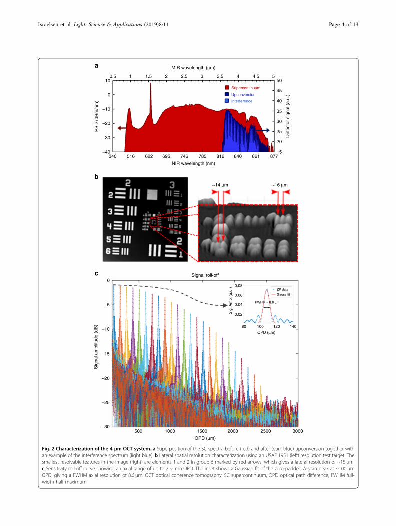
scanning a USAF 1951 resolution test target. The trans-lation speed of the fast (horizontal) scanning axis was setto 3 mm/s, and with an integration time of 3 ms per linefor maximum signal, 1000 line scans were performed in3 s, resulting in a 9-μm horizontal sampling resolution.Along the slow (vertical) scanning axis of the stage, theresolution is determined by the step size of the scanner,which was set to 10 μm. From Fig. 2b, it is shown that thesystem is able to resolve elements 1 and 2 of group 6,which results in a lateral resolution of ~15 μm. Todetermine the axial resolution, the sensitivity, and thesensitivity roll-off, a plane mirror was positioned in thesample arm and the resulting interferograms wererecorded for different one-way optical path difference(OPD) values by translating the mirror in the referencearm.Figure 2c displays the sensitivity roll-off for 3-mm
translation, which can be used to infer the effective ima-ging depth of the system. From the 6 dB roll-off of 1.35mm, the corresponding mid-IR spectral resolution wasdetermined to be 2.7 nm. From the same data, an axialresolution of 8.6 µm is found at an OPD of ~100 µm (seeinset of Fig. 2c) and better than 9 µm within the first1 mm. Therefore, even for such a long center wavelength,the axial resolution in air is similar to values reported for
Israelsen et al. Light: Science & Applications (2019) 8:11 Page 3 of 13
0.510 50
45
40
35
30
25
20
15
0
–10
–20
–30
–40
0
–5
–10
–15
–20
–25
–30500 1000 1500
OPD (μm)
OPD (μm)
Signal roll-off
Sig
. Am
p. (
a.u.
) 0.08
0.06
0.04FWHM = 8.6 μm
ZP data
Gauss fit
0.02
80 100 120 140
~14 μm ~16 μm
2000 2500 3000
340 516 622 695
NIR wavelength (nm)
746 785 816 840
Supercontinuum
Upconversion
Interference
861 877
1 1.5 2 2.5
MIR wavelength (μm)a
b
c
PS
D (
dBm
/nm
)S
igna
l am
plitu
de (
dB)
Det
ecto
r si
gnal
(a.
u.)
3 3.5 4 4.5 5
Fig. 2 Characterization of the 4-μm OCT system. a Superposition of the SC spectra before (red) and after (dark blue) upconversion together withan example of the interference spectrum (light blue). b Lateral spatial resolution characterization using an USAF 1951 (left) resolution test target. Thesmallest resolvable features in the image (right) are elements 1 and 2 in group 6 marked by red arrows, which gives a lateral resolution of ~15 μm.c Sensitivity roll-off curve showing an axial range of up to 2.5-mm OPD. The inset shows a Gaussian fit of the zero-padded A-scan peak at ~100 μmOPD, giving a FWHM axial resolution of 8.6 μm. OCT optical coherence tomography, SC supercontinuum, OPD optical path difference, FWHM full-width half-maximum
Israelsen et al. Light: Science & Applications (2019) 8:11 Page 4 of 13
near-IR systems at 1.7 and 2 µm15,17–19. In the best case, asensitivity of 60 dB is obtained, which is significantlylower than the 90 dB sensitivity of the 1.3-µm OCT sys-tem used for the near-IR comparison (see Supplementarysection IV for details).
Mid-IR OCT in comparison to near-IR OCT: proof-of-principleAs an example of the improved penetration of the mid-
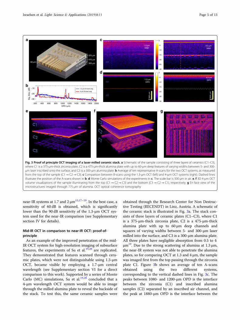
IR OCT system for high-resolution imaging of subsurfacefeatures, the experiments of Su et al.19,28 are replicated.They demonstrated that features scanned through cera-mic plates, which were not distinguishable using 1.3-µmOCT, became visible by employing a 1.7-µm centralwavelength (see Supplementary section VI for a directcomparison to this work). Supported by a series of MonteCarlo (MC) simulations, Su et al.19,28 concluded that a4-μm wavelength OCT system would be able to imagethrough the milled alumina plate to reveal the backside ofthe stack. To test this, the same ceramic samples were
obtained through the Research Center for Non Destruc-tive Testing (RECENDT) in Linz, Austria. A schematic ofthe ceramic stack is illustrated in Fig. 3a. The stack con-sists of three layers of ceramic plates (C1–C3), where C1is a 375-μm-thick zirconia plate, C2 is a 475-μm-thickalumina plate with up to 60 μm deep channels andsquares of varying widths between 5- and 300-μm lasermilled into the surface, and C3 is a 300-μm alumina plate.All three plates have negligible absorption from 0.5 to 4μm19. Due to the strong scattering of alumina at 1.3 μm,the near-IR system was not able to penetrate the aluminaplates, so for comparing OCT at 1.3 and 4 μm, the samplewas imaged first from the top passing through the zirconiaplate C1. Figure 3b shows an average of ten A-scansobtained using the two different systems,corresponding to the vertical dashed lines in Fig. 3c. Thepeaks between 1080- and 1200-μm OPD is the interfacebetween the zirconia (C1) and inscribed aluminasamples (C2) separated by an inscribed air channel, andthe peak at 1880-μm OPD is the interface between the
–10
0
–5
–10
–15
–20
–25
–30
0
–5
–10
–15
–20
–25
–30
a c
b
d
e f g
–20
–30Sig
. Am
p. (
dB)
200 400 600 800 1000OPD (μm)
1200 1400
1.3 μm A-scan avg.
4 μm A-scan avg.
1600 1800 2000
C11.3 μm(exp)
375 μm
60 μm475 μm
300 μmC1 Zirconia
C2 Alumina
C3 Alumina
4.0 μm(exp)
4.0 μm(sim)1.3 μm
(sim)
500
μm
500
μm
C2
C1
C2
Fig. 3 Proof of principle OCT imaging of a laser-milled ceramic stack. a Schematic of the sample consisting of three layers of ceramics (C1–C3),where C1 is a 375-μm-thick zirconia plate, C2 is a 475-μm-thick alumina plate with up to 60-μm deep features of varying widths between 5- and 300-μm laser inscribed onto the surface, and C3 is a 300-μm alumina plate. b Average of ten representative A-scans for the two OCT systems, as measuredfrom the top of the sample (C1→ C2→ C3). c Comparison between B-scans using the 1.3-μm OCT (left) and 4-μm OCT systems (right). Dashed linesillustrate the position of the A-scans shown in b. d Monte Carlo simulations of the experiments in c. The scale bar is 500 μm in air. e, f 3D 4-μm OCTvolume visualizations of the sample illuminating from the top (C1→ C2→ C3) and the bottom (C3→ C2→ C1), respectively. g En face view of themicrostructures imaged through 775 μm of alumina. OCT optical coherence tomography
Israelsen et al. Light: Science & Applications (2019) 8:11 Page 5 of 13
two alumina plates (C2 and C3). The thickness of theplates can then be calculated by dividing the OPDthickness (809.9 μm for C1 and 787.0 μm for C2) by therefractive indices (2.138 at for zirconia and 1.675 foralumina)19, resulting in 378.8 ± 3.8 and 469.9 ± 4.9 μm forC1 and C2, respectively, with the uncertainty corre-sponding to twice the sampling resolution divided by therefractive index. Both thicknesses are very close to thevalues measured using the mechanical thickness gauge,especially considering the uncertainty of therefractive indices. Figure 3c shows the corresponding B-scans obtained using the two OCT systems. By comparingthe two images, it is clear that the mid-IR signal pene-trates deeper into the sample and is able to resolve theboundary between C1 and C2 with a higher contrast, as
well as the boundary between C2 and C3. The 1.3-μmOCT system provides only a weak signal from the C1 toC2 boundary despite the much higher sensitivity. Thisresult is consistent with the findings of Su et al.19; tofurther support this finding, a series of MC simulationswere performed (see Methods for details). The simula-tions, shown in Fig. 3d, qualitatively confirm the improvedvisualization of the in-depth interfaces in the 4-μm OCTimages (see also Supplementary video I). Figure 3e showsa 3D visualization of the sample over a 5.6 mm × 7.3 mmscanned area, which shows strong localizedscattering centers from within the porous C1 layer and aclear identification of the laser-milled structures belowthe C1–C2 interface (see also Supplementary videos IIand III).
0P3
–10
Sig
. am
p. [d
B]
Incr
easi
ng a
lum
ina
thic
knes
s
Alumina tape
P1
P1
P2
P3
P4
P5
P1
100 μm (air)
P2
P3
P4
P5
P2
P3
P4
P5
1.3 μm OCT 4 μm OCT
–20
–30100 200
: air/foil interface : Al2O3 layer : ghost images: B-scan region
1.3 μm OCT
4 μm OCT
300 400
Multiple scattering
OPD (relative) [μm]
500 600 700 800
Fig. 4 Demonstration of the reduction in multiple scattering at 4 μm. Left: Top-view photograph of the alumina on cellulose acetate foil withgreen dotted lines indicating the different B-scan sections P1–P5. It should be noted that P1 is a reference point where there is no alumina depositedon the foil. Middle: Sample B-scans at positions P1–P5 using the 1.3-μm OCT system showing the detrimental effect of multiple scattering. Rightcorresponding sample B-scans at positions P1–P5 using the 4-μm OCT system showing significantly reduced scattering. Bottom average of ten A-scans (corresponding to the vertical dashed lines at P3) for both OCT systems
Israelsen et al. Light: Science & Applications (2019) 8:11 Page 6 of 13
To further test the penetration capability of the 4-μmsystem, the stack was imaged from the bottom throughthe C3 alumina plate. Figure 3f shows a 3D scan of thisconfiguration, which surprisingly reveals a significantlyimproved signal from the backside C2–C1 interfacedespite having traveled through 775 μm of alumina. Asseen in Fig. 3g, the microstructures are clearly resolved,revealing the surface roughness from inside the milledareas (see Supplementary Fig. S1). This demonstrates thecapability of the mid-IR OCT system to perform high-resolution imaging in scattering media. Due to the highspatial sampling resolution and maximum integrationtime used, the 800 × 730 × 2048 pixel volume took36.5 min to acquire.
Multiple scattering, dispersion, and non-uniform samplesIn the experiments with the ceramic plates, the reduced
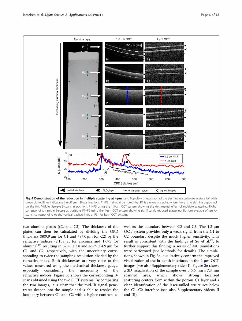
scattering at longer wavelengths clearly resulted inimproving the imaging depth. However, for highly scat-tering materials, OCT imaging is severely impaired notonly by the reduced penetration depth but also by thescrambling of the spatial image information through theeffect of multiple scattering. To illustrate this, a sample
consisting of a highly scattering alumina green tape ofvarying thickness applied to a cellulose acetate foil of ~62-μm thickness was imaged with the near-IR and mid-IROCT systems. Figure 4 shows a photograph of the samplewith annotations to indicate the scanned regions P1–P5,where the thickness of the alumina tape increases from P1to P5. The corresponding B-scans for the two systems arepresented in adjacent columns for direct comparison. P1corresponds to a B-scan of the acetate foil only, while thefollowing images (P2–P5) portray the effect of theincreased thickness of the alumina tape imaged by the twosystems. It is clear from the B-scans using the 1.3-μmOCT system that a band of multiple scattered signalsincreasing in thickness from P2 to P5 eventually obscuresthe acetate–air interface in P4 and P5, extending theapparent thickness of the alumina tape beyond its physicalextension. However, in the images acquired using the 4-μm OCT system, the integrity of the spatial information isretained and the thickness of the alumina tape can beevaluated. Sectioning the structure along P3, the backsideof the acetate foil (n= 1.48) is just barely resolved with1.3-μm OCT, while it can be clearly seen in the 4-μm B-scan. From the latter, the thickness of the alumina film
Dispersion in a silicon wafer
1.3 μm OCT
B-scan B-scan
Air/Si interface Ghost signal
250 μm
250 μm
Amp. [dB]
0
–10
–20
0
–10
–20
–30
0
–10
–20
–30
250300
350400
4501150
12001250
1300
0
–10
–20
680700
FWHM
FWHM
~5 μm
FWHM
FWHM
~12 μm
~17 μm~18 μm
720
OP
D [μm
]
OP
D [μm
]O
PD
[μm]
OP
D [μm
]
7401620
16401660
1680
Amp. [dB]
4 μm OCT
Fig. 5 Demonstration of the reduction in dispersion at 4 μm. B-scans of a 255-μm-thick silicon wafer using the 1.3 μm (left) and 4 μm (right) OCTsystems showing broadening of the A-scan peak from 5 to 18 μm and from 12 to 17 μm, respectively. Note that the peaks at the air–silicon interfacesdeviate from the best-case resolution due to spectral apodization. OCT optical coherence tomography
Israelsen et al. Light: Science & Applications (2019) 8:11 Page 7 of 13
(n ~1.68)19 is estimated to be just 24 μm, but the multiplescattered signals in the B-scan image at 1.3 μm extend allthe way beyond the backside of the acetate foil. Thestrong scattering of the 1.3-μm light indicates that theporous structure of the alumina layer is comparable insize to the wavelength, which is consistent with the 0.5-μmmean pore diameter for alumina reported in Su et al19.The significant reduction in multiple scattering goingfrom 1.3 to 4 μm therefore represents the transition fromthe domain of strong directional Mie scattering with ashort photon mean-free path to the domain of weakeruniform Rayleigh scattering having a long photon mean-free path, compared to the wavelength of light.The mid-IR OCT system can also have an advantage
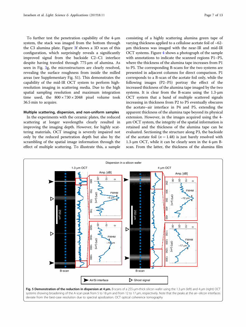
even in highly uniform and transparent media, such asgermanium due to its bandgap in the near-IR, or silicondue to its lower group-velocity dispersion (GVD) at 4 μm.The effect of dispersion is to introduce a difference indelay between the short and long wavelengths of thespectrum, which in turn results in broadening of the
backscattered signal. For this reason, the correct depthresolved information in OCT can only be obtained afterdispersion compensation29. To illustrate this, a 255-μm-thick (±5 µm) silicon wafer was imaged using the twosystems having a GVD of 1576 and 385fs2/mm at 1.3 and4 μm, respectively30. At 1.3 μm, the strong dispersionresults in significant broadening of the reflection peak ofthe wafer from 5 to 18 μm full-width at half-maximum(FWHM), whereas at 4 μm the peak broadened sig-nificantly less from 12 to 17 μm FWHM, as seen in Fig. 5.As a result, the image distortion due to dispersion is lesspronounced in the 4-μm OCT system, which could beuseful for characterization of silicon-based devices, suchas micro electromechanical systems, solar cells, andwaveguides. The thicknesses measured with the 4- and1.3-µm OCT systems are 250.6 ± 1.7 and 263.0 ± 0.79 µm,respectively, when accounting for the refractive indicesand with the uncertainty given by the digital sampling.The discrepancy in the measured thicknesses is attributedto the strong dispersion at 1.3 µm.
a
b
c
d
Bonded wire Contactcircuitry
Si-microprocessor
4 μm B-scan1.3 μm B-scan
Cross section Encapsulation layers
Metal contact interface
Antenna layer
Card backside
P1
P2
P3
Contactlessantenna interface
EN face
EMV chip
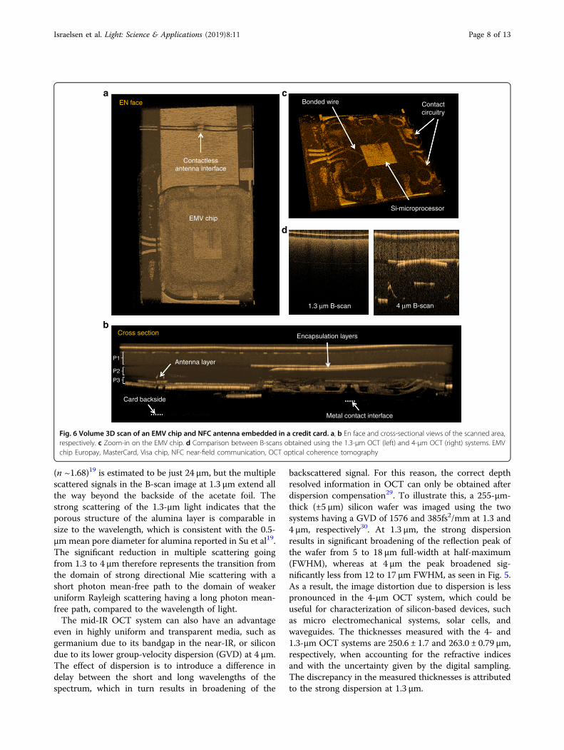
Fig. 6 Volume 3D scan of an EMV chip and NFC antenna embedded in a credit card. a, b En face and cross-sectional views of the scanned area,respectively. c Zoom-in on the EMV chip. d Comparison between B-scans obtained using the 1.3-μm OCT (left) and 4-μm OCT (right) systems. EMVchip Europay, MasterCard, Visa chip, NFC near-field communication, OCT optical coherence tomography
Israelsen et al. Light: Science & Applications (2019) 8:11 Page 8 of 13
Finally, to demonstrate 3D imaging of more complexnon-uniform structures, a Europay, MasterCard, Visa-chip (EMV chip) and a near-field communication antennaembedded in a standard credit card are imaged at 4 μm.Credit cards are commonly made from several layers oflaminated polymers mixed with various dyes and addi-tives. An overview of the scanned chip area is shown inFig. 6a, b in an en face and cross-sectional view, respec-tively (see also Supplementary video IV and Supplemen-tary Fig. S2). Underneath the thin transparent surface,three layers of highly scattering polymers are identified,which are seen most clearly at the edges of Fig. 6b asbright uniform bands (P1–P3) separated by dark lines. Asseen in Fig. 6d, the polymer is so scattering in the near-IRthat even the top most layer (P1) cannot be penetrated bythe 1.3-μm OCT system. On the other hand, the 4-μmOCT system is able to resolve all three polymer layers andcan in some places even detect the backside of the card,which is 0.76 mm thick. Below the first scattering polymerlayer, the first structure to appear is the encapsulationlayer protecting the embedded silicon microprocessor.The bonded wires and circuitry connecting the micro-processor to the underlying gold contact pad are alsoclearly visible, as seen in Fig. 6c.
DiscussionFrom the images of various samples presented here, it
would seem that the 4-μm OCT system is superior tothe 1.3-μm OCT system in every aspect. Even with asignificantly reduced sensitivity, the reduced scatteringat 4 μm allows clear depth resolved imaging of inter-faces from samples considered too thick for the 1.3-μmOCT system. The increased water absorption at longwavelengths naturally excludes biological samples, butexcept for a group of carboxylic acids, the spectralregion of 3.6–4.6 μm is remarkably devoid of vibra-tional resonances, making it ideal for NDT using OCT.It is therefore expected that most materials and sam-ples with low water content, that are currently beinganalyzed at 1.3 μm but are limited to a penetrationdepth of few tens to hundreds of microns due toscattering, can benefit from being imaged at 4 μm. Themeasured axial resolution is 8.6 µm, which agrees wellwith the expected value for a zero-padded harmonicallymodulated spectrum ranging from 3576 to 4625 nm,obtained for the shortest OPDs. To improve the reso-lution further, it is necessary to increase the bandwidthof the detected spectrum beyond the already remark-ably broad >1-µm bandwidth, which is currently lim-ited by the bandwidth of the upconversion scheme andthe long-wavelength edge of the SC source. The sen-sitivity roll-off is currently limited by the radiallyvarying spatial mode profile from the upconversionmodule, which enforces the use of a large multimode
fiber as the limiting aperture for the spectrometer. Thiscould be optimized if the upconverted beam could beefficiently transformed to match the fundamental modeof a single-mode collecting fiber, for which the spec-trometer was designed. One way of achieving this couldbe implementing aperiodic poling of the nonlinearcrystal31,32 to satisfy collinear phase matching over abroad spectral range and thus enabling single-modefiber coupling to the spectrometer. Fulfilling this, thespectral resolution can be made comparable to thesampling resolution of the spectrometer, thusincreasing the maximum image depth of the system.According to the characterization made by the manu-facturer, the maximum image depth supported by thespectrometer is 8.6 mm, which is possible since only a15 dB attenuation is expected using an optimizedsingle-mode spot size. Approaching a centimeter inoptical path length would pave the way to a whole newseries of NDT applications where both imaging atmacroscopic length scales along with microscopicdetails are required. In the end, a compromise betweenthe upconversion efficiency, the upconversion band-width and the properties of the output spatial modemust be achieved. To reach 90 dB sensitivity, theupconversion efficiency has to be increased tenfold. Inthis regard, new upconversion schemes under devel-opment may allow an increase in the intracavity powerto as much as 100–150W, thus improving the effi-ciency by a factor of 3–5. Similarly, the acquisitionspeed could be improved through increased conversionefficiency or by increasing the signal power, to reducethe integration time of the spectrometer.In conclusion, fast real-time spectral-domain OCT
imaging in the mid-IR was demonstrated using an SCsource in combination with parallelized frequencyupconversion covering more than 1µm bandwidth from3.58 to 4.63 μm. The broad bandwidth resulted in anaxial resolution as high as 8.6 µm, which together with alateral resolution of 15 µm enabled detailed imaging ofmicroscopic structures embedded in media that arehighly scattering at the more conventional 1.3-µmwavelength. The upconverted signal was measured usinga Si-CMOS spectrometer acquiring data with a line rateof 0.33 kHz, which enabled real-time B-scans at mm/sspeed, and C-scans at mm2/min acquisition rate. Todemonstrate the superiority of mid-IR OCT, compara-tive data have been presented using an ultra-high-resolution OCT system at the more conventional 1.3-µm wavelength. To validate the results, samples wereassembled similar to those used in other previousreports. Through the realization of real-time mid-IROCT imaging, this work bridges the gap between tech-nology and practical applications of mid-IR OCT as anindustry-ready tool for NDT.
Israelsen et al. Light: Science & Applications (2019) 8:11 Page 9 of 13
Materials and methodsSC generationThe SC source was pumped by a four-stage MOPA using
an unfolded double-pass amplifier configuration based on a1.55-μm directly modulated seed laser diode. The seedpulse duration is 1 ns, and the repetition rate is tunablebetween 10 and 10MHz. The seed is subjected to threestages of amplification in erbium- and erbium-ytterbium-doped silica fibers, which extends the spectrum to 2.2 μmby in-amplifier nonlinear broadening. To further push thespectrum towards longer wavelengths, the erbium fiber wasspliced to ~40 cm of the 10-μm core diameter thulium-doped double-clad fiber, which extended the spectrum to2.7 μm. The thulium-doped fiber was subsequently splicedto a short piece of silica mode-field adapter fiber having amode-field diameter of 8 μm, which provided a bettermatch to the fluoride fiber. The mode adapter fiber is butt-coupled to a 6.5-μm core diameter single-mode ZrF4-BaF2-LaF3-AlF3-NaF (ZBLAN) fiber from FiberLabs Inc., with ashort length of approximately 1.5m to reduce the effect ofstrong multiphonon absorption beyond 4.3 μm.
InterferometerThe interferometer is based on a Michelson design
employing a gold-coated parabolic mirror collimator, abroadband CaF2 wedged plate beam splitter, a BaF2 plano-convex lens in the sample arm, and a BaF2 window andflat silver mirror in the reference arm. The BaF2 lens waschosen to minimize the effect of dispersion, while beingavailable at a relatively short focal length of 15 mm. At4 μm, the dispersion of BaF2 is relatively low at 16.4 ps/nm/km compared to other standard lens substrates, suchas CaF2 (33.0), Si (−45.8), and ZnSe (−59.9), but mostimportantly, the dispersion slope is flat from 3.5–4.5 μm(13.6–19.1 ps/nm/km)33. Even so, the residual dispersionfrom the 6.3-mm center thickness lens was roughlycompensated by a 5-mm window and the remaining dis-persion was compensated numerically. Coupling to theupconversion module was performed using a 6-mm focallength aspheric chalcogenide lens and a 9-μm core dia-meter single-mode indium fluoride patch cable.
UpconversionUpconversion is realized by mixing the low-energy IR
photons at a wavelength λIR with pump photons at awavelength λP to generate upconverted photons with awavelength λUP, under energy and momentum con-servation:
λ�1P þ λ�1
IR ¼ λ�1UP;Δ
~k ¼~kUP �~kP �~kIR ð1Þ
where ~k is the wave propagation vector and Δ~k is ameasure of the phase mismatch among the three inter-acting waves, which should ideally be zero for maximum
QE. Furthermore, the QE scales linearly with the pumppower and scales quadratically with the effective nonlinearcoefficient (deff) and the length of the nonlinear med-ium27. The mid-IR OCT system is operated at a wave-length of 4 µm with a spectral bandwidth >1 µm.Accordingly, the upconversion module was designed andoptimized to upconvert the entire spectral range from 3.6to 4.6 μm for the fastest detection. Among the variousphase-matching configurations, quasi-phase matching ina PPLN crystal was chosen for the broadband upconver-sion, owing to its design flexibility, access to a high deff(14 pm/V), and optical transparency up to 5 µm26. Theupconversion took place inside the PPLN crystal, whereeach wavelength was phase-matched at a different pro-pagation angle. Thus, noncollinear interaction among thethree participating waves was used to phase match over awide spectral range (see Supplementary Fig. S3a). As theλUP is below λP, by choosing the pump wavelength λP=1µm, conventional Si-CMOS detection can be engaged forλUP. Here, a solid-state (Nd:YVO4) CW linearly polarizedlaser operating at 1064 nm was used as the pump. Thiswas driven by a broad area emitting laser diode (3W,880 nm). The high-finesse folded solid-state laser cavitywas formed by mirrors M1–M7 (see SupplementaryFig. S4). All mirrors are high-reflective coated for 1064 nmand anti-reflective (AR) coated for 700–900 nm. Themirror M7 is based on an undoped YAG substrate andadditionally high-transmission -coated for the 2–5-µmrange. The mirror M6 acts as an output coupler for theupconverted light. The mirrors M4 and M5 are placed ina separate compartment to filter out the fluorescencefrom the laser crystal and 880-nm pump laser. A 20-mm-long 5% MgO-doped PPLN crystal is used for theexperiment (Covesion, AR-coated for 1064 nm,2.8–5.0 µm on both facets). The PPLN crystal consists offive different poling periods (Λ) ranging from 21 to 23 µmin steps of 0.5 µm. Each poled grating has a 1 mm× 1mmaperture and is separated by 0.2-mm-wide regions ofunpoled material. For different values of Λ, the phasemismatch and hence the overall upconversion spectralbandwidth varies (see Supplementary Fig. S3b). A widerbandwidth requires larger input angles for the IR beam,which reduces the overall QE as the effective interactionlength is reduced. For a best-case scenario, Λ= 23 µm wasconsidered in the setup. A CW intracavity power of >30W at 1064 nm was realized with a spot size (beam radius)of 180 µm inside the PPLN crystal. The entire system isoperated at room temperature. The estimated maximumQE at each mid-IR wavelength is plotted in Supplemen-tary Fig. S3c, considering an effective interaction length of20 mm inside the PPLN crystal. The IR light (output ofthe fiber coupled 4-µm OCT signal) is collimated andthen focused into the PPLN crystal using a pair of CaF2aspheric lenses (f= 50mm, AR coated for 2–5 µm). The
Israelsen et al. Light: Science & Applications (2019) 8:11 Page 10 of 13
upconverted light is collimated by a silica lens (f= 75mm,AR coated for 650–1050 nm). A shortpass 1000-nm filterand a longpass 800-nm filter are inserted to block theleaked 1064-nm beam and 532-nm parasitic second har-monic light, respectively. A schematic representation ofthe radial wavelength distribution across the transverseupconverted beam profile is shown in SupplementaryFig. S4. The module is able to upconvert all wavelengthsin a broad mid-IR spectral range of 3.6–4.8 µm to820–870 nm, simultaneously.
Detection, scanning, and data processingAfter the upconversion module, the near-IR light is
collected by a 100-µm core multimode silica fiber guidingthe light to a line scan spectrometer (Cobra UDC,Wasatch Photonics, USA) operating with a maximum linerate of 45 kHz (for a bit depth of 10). The spectral rangecovered the wavelengths of 796 to 879 nm, which issampled by 4096 pixels. To scan the sample, it is mountedon a double translation stage (2 × ILS50CC from New-port) with a maximum travel speed of 100mm/s, a travelrange of 50 mm and a stepping resolution of 1 µm. Thedetected raw spectra are dark signal subtracted and nor-malized to the reference arm signal. Pixel to wavenumbertranslation and interferometer dispersion compensationare achieved by exploiting the phase information acrossthe pixel array retrieved for two reference interferogramsshowing clear interference fringes. In this way, spectralresampling is performed to linearize wavenumber sam-pling34, after which a phase shift is applied for compen-sating the unevenly matched dispersion in the arms of theinterferometer. To suppress the effects stemming fromthe spectral envelope of the interferograms, a Hanningspectral filter is applied to the spectral region of theinterferometric signals. Finally, a fast Fourier transform isapplied to generate a reflectivity profile, that is, an A-scan.A compromise between signal strength and acquisitiontime is made that leads to an A-scan acquisition time of 3ms. To build B-scans (2D images), the horizontal stage (X)is programmed to move continuously over a specifieddistance, achieving a 500 line B-scan in 1.5 s. 3D scans arebuilt by stepping the vertical (Y) stage at a proportionatelyslower rate to assemble multiple B-scans.
MC simulationsThe MC simulations are performed using the open
source software MCX35. The simulated domain consistsof 1400 × 9 × 230 uniform voxels in XYZ with a size of 5 ×5 × 5 μm3 each, corresponding to a total size of 7000 ×45 × 1150 μm3. The structure is considered uniform alongthe Y direction, similar to what is shown in the ridge/valley part of Fig. 3a. The slab thicknesses and the valleydepths in the simulation are identical to the real ones, butthe valley widths in the simulation increase along the
horizontal direction from 5 μm at one side of the domainto 180 μm to the other side in steps of 5 μm for the sake ofsimplicity. The optical properties of zirconia and aluminaused in the MC simulations are taken from Su et al19. TheMC software launches a number of photons into thedefined structure and tracks their path taking intoaccount the refractive index, absorption, scattering, andscattering anisotropy using a random number generatorto emulate scattering statistics. The simulated source usesa beam with a Gaussian transverse distribution with aconstant width (5 μm for 1.3-µm center wavelength, and15 μm for 4-µm center wavelength), due to the MCsimulations being pure geometrical optics, which hindersthe use of a diverging Gaussian beam. The OCT signal ina single A-scan is extracted from the MC simulation by, ateach time step, summing the flux of photons that returnto the top layer of the simulation within an angle corre-sponding to the NA of the system, which is 0.1 for both1.3 and 4 µm. The simulations thus emulate a time-domain OCT implementation. The simulations ran forT= 14.4 ps, in steps of dt= 24 fs, giving a digital samplingof dz= (c dt)/ 2= 3.6 µm in air. Due to the lack of wavenature of light in the MC simulations, both the axial andlateral resolutions are limited by the digital sampling only,which is unphysical of course, but accepted here becausethe investigation focuses on the comparison of thepenetration depth. The B-scans are constructed by col-lecting A-scans obtained by moving the source 10 µmlaterally, which gives 700 A-scans in a B-scan. Each A-scan simulation is performed using a different seed for therandom number generator. To make the raw B-scansrepresent their experimental counterparts, they are cor-rected for roll-off by multiplying each A-scan with themeasured roll-off curve, as well as corrected for thereduction in signal strength caused by the divergence ofthe Gaussian beam. This correction is introduced bymultiplying the signal at a given depth, z, by the overlapintegral, C, between the fundamental mode of the fiberthat collects the light and the transverse distribution ofthe light reflected at z. This overlap integral is approxi-mated here by the overlap integral between the Gaussiandistribution of the propagating beam at the focal point U(x,y,zF) and the transverse distribution of light that isreflected at another point z>zF. Due to the double passof light, the second distribution becomes Gaussian likethe input beam at a distance 2(z− zF) from the focalpoint:
C �R R1
�1U x; y; 2z � zFð ÞU x; y; zFð Þdxdy� �2R R1
�1U x; y; 2z � zFð Þ2dxdyR R1�1U x; y; zFð Þ2dxdy
¼ 4w40π
2 4 z � zFð Þ2λ2 þ π2w40
� �
4 z � zFð Þ2λ2 þ 2π2w40
� �2
ð2Þ
Israelsen et al. Light: Science & Applications (2019) 8:11 Page 11 of 13
where U(x,y,z) represents a Gaussian beam with e–2 widthw0. The focal point, zF, is placed 50 µm below the topsurface of C1 to emulate the experimental conditions. Theexact parameters and options input to the MCX softwareas well as the files specifying the spatial domain and theoverlap integrals are freely available from the authorsupon request.
AcknowledgementsWe acknowledge the financial support from Innovation Fund Denmarkthrough ShapeOCT Grant No. 4107-00011A. A.P. acknowledges the NIHRBiomedical Research Center at Moorfields Eye Hospital NHS Foundation Trustand the UCL Institute of Ophthalmology and the Royal Society WolfsonResearch Merit Award. D.J. acknowledges the support from H.C. ØrstedCOFUNDED Marie-Curie action fellowship, and financial support from H. C.Ørsted for the running cost. We would also like to thank the following people:Dr. Lasse Høgstedt of NLIR, Nonlinear Infrared Sensors, for helpful discussionsregarding the upconversion system, Andreas Buchsbaum, former employee atRECENDT for help in providing the test samples, Dr. Rong Su of NottinghamUniversity for supplying the ceramic samples, Dr. Michael Maria of KentUniversity for fruitful discussions regarding the OCT part, and Brian Sørensen ofDTU Fotonik for assistance with the control electronics.
Author details1DTU Fotonik, Technical University of Denmark, 2800 Kgs, Lyngby, Denmark.2NORBLIS IVS, Virumgade 35 D, Virum 2830, Denmark. 3Research Center forNon-Destructive Testing (RECENDT), Altenberger Straße 69, 4040 Linz, Austria.4NLIR ApS, Hirsemarken 1, Farum 3520, Denmark. 5Applied Optics Group,School of Physical Sciences, University of Kent, Canterbury CT2 7NH, UK
Author contributionsO.B. was the principal investigator setting up the consortium and raising thefunding for the project. N.M.I., C.R.P., and A.B. were mainly responsible for theexperimental work and manuscript writing. N.M.I. together with C.R.P. and A.P.were responsible for the 4-µm OCT system. C.R.P. together with D.J. and O.B.was responsible for the SC source. A.B. together with P.T.-L. and C.P. wasresponsible for the upconversion detection system. N.M.I. together with A.P.was responsible for the 1.3-µm OCT system. M.J. was responsible for the 1.3and 4-µm MC simulations. G.H. was responsible for supplying the test samples.All authors discussed the results and contributed to the finalization of themanuscript.
Conflict of interestThe authors declare no competing interest.
Supplementary information is available for this paper at https://doi.org/10.1038/s41377-019-0122-5.
Received: 6 July 2018 Revised: 7 January 2019 Accepted: 7 January 2019
References1. Huang, D. et al. Optical coherence tomography. Science 254, 1178–1181
(1991).2. Shemonski, N. D. et al. Computational high-resolution optical imaging of the
living human retina. Nat. Photonics 9, 440–443 (2015).3. Siddiqui, M. et al. High-speed optical coherence tomography by circular
interferometric ranging. Nat. Photonics 12, 111–116 (2018).4. Robles, F. E., Wilson, C., Grant, G. & Wax, A. Molecular imaging true-colour
spectroscopic optical coherence tomography. Nat. Photonics 5, 744–747(2011).
5. Targowski, P. & Iwanicka, M. Optical coherence tomography: its role in thenon-invasive structural examination and conservation of cultural heritageobjects—a review. Appl. Phys. A 106, 265–277 (2012).
6. Stifter, D. Beyond biomedicine: a review of alternative applications anddevelopments for optical coherence tomography. Appl. Phys. B 88, 337–357(2007).
7. Zeitler, J. A. & Gladden, L. F. In vitro tomography and non-destructive imagingat depth of pharmaceutical solid dosage forms. Eur. J. Pharm. Biopharm. 71,2–22 (2009).
8. Swanson, E. A. & Fujimoto, J. G. The ecosystem that powered the translation ofOCT from fundamental research to clinical and commercial impact [Invited].Biomed. Opt. Express 8, 1638–1664 (2017).
9. Koller, D. M., Hannesschläger, G., Leitner, M. & Khinast, J. G. Non-destructiveanalysis of tablet coatings with optical coherence tomography. Eur. J. Pharm.Sci. 44, 142–148 (2011).
10. Stifter, D. et al. Investigation of polymer and polymer/fibre compositematerials with optical coherence tomography. Meas. Sci. Technol. 19, 074011(2008).
11. Cho, N. H., Jung, U., Kim, S. & Kim, J. Non-destructive inspection methods forLEDs using real-time displaying optical coherence tomography. Sensors 12,10395–10406 (2012).
12. Czajkowski, J., Prykäri, T., Alarousu, E., Palosaari, J. & Myllylä, R. Optical coherencetomography as a method of quality inspection for printed electronics pro-ducts. Opt. Rev. 17, 257–262 (2010).
13. Prykäri, T., Czajkowski, J., Alarousu, E. & Myllylä, R. Optical coherence tomo-graphy as an accurate inspection and quality evaluation technique in paperindustry. Opt. Rev. 17, 218–222 (2010).
14. Su, R. et al. Optical coherence tomography for quality assessment ofembedded microchannels in alumina ceramic. Opt. Express 20, 4603–4618(2012).
15. Cheung, C. S., Daniel, J. M. O., Tokurakawa, M., Clarkson, W. A. & Liang, H. Highresolution Fourier domain optical coherence tomography in the 2 μmwavelength range using a broadband supercontinuum source. Opt. Express23, 1992–2001 (2015).
16. Cheung, C. S., Daniel, J. M. O., Tokurakawa, M., Clarkson, W. A. & Liang, H.Optical coherence tomography in the 2-μm wavelength regime for paint andother high opacity materials. Opt. Lett. 39, 6509–6512 (2014).
17. Sharma, U., Chang, E. W. & Yun, S. H. Long-wavelength optical coherencetomography at 1.7 μm for enhanced imaging depth. Opt. Express 16,19712–19723 (2008).
18. Ishida, S. & Nishizawa, N. Quantitative comparison of contrast andimaging depth of ultrahigh-resolution optical coherence tomographyimages in 800–1700 nm wavelength region. Biomed. Opt. Express 3, 282–294(2012).
19. Su, R. et al. Perspectives of mid-infrared optical coherence tomography forinspection and micrometrology of industrial ceramics. Opt. Express 22,15804–15819 (2014).
20. Colley, C. S et al. Mid-infrared optical coherence tomography: application intissue engineering. In Biomedical Topical Meeting 2006 (OSA, Fort Lauderdale,2006) http://www.osa.org/osaorg/media/osa.media/Meetings/Archives/2006/biomed/BIOMED_2006_Final_Archive.pdf.
21. Colley, C. S. et al. Mid-infrared optical coherence tomography. Rev. Sci. Instrum.78, 123108 (2007).
22. Varnell, D., Zheng, M. C., Chow, M. & Gmachl, C. Spectroscopy andimaging using a mid-IR quantum cascade optical coherence tomography(OCT) system. In CLEO: Applications and Technology 2016 (OSA, San Jose,2016).
23. Paterova, A. V., Yang, H. Z., An, C. W., Kalashnikov, D. A. & Krivitsky, L. A. Tunableoptical coherence tomography in the infrared range using visible photons.Quantum Sci. Technol. 3, 025008 (2018).
24. Israelsen, N. M. et al. The value of ultrahigh resolution OCT in dermatology—delineating the dermo-epidermal junction, capillaries in the dermal papillaeand vellus hairs. Biomed. Opt. Express 9, 2240–2265 (2018).
25. Petersen, C. R., Moselund, P. M., Huot, L., Hooper, L. & Bang, O. Towards a table-top synchrotron based on supercontinuum generation. Infrared Phys. Technol.91, 182–186 (2018).
26. Dam, J. S., Tidemand-Lichtenberg, P. & Pedersen, C. Room-temperature mid-infrared single-photon spectral imaging. Nat. Photonics 6, 788–793(2012).
27. Pedersen, C., Karamehmedović, E., Dam, J. S. & Tidemand-Lichtenberg, P.Enhanced 2D-image upconversion using solid-state lasers. Opt. Express 17,20885–20890 (2009).
Israelsen et al. Light: Science & Applications (2019) 8:11 Page 12 of 13
28. Su, R., Chang, E., Ekberg, P., Yun S. & Mattsson L. Enhancement of probingdepth and measurement accuracy of optical coherence tomography formetrology of multi-layered ceramics. In Proc. 1st International Symposium onOptical Coherence Tomography for Non-Destructive Testing 71–73 (Linz, Austria,2013) http://www.diva-portal.org/smash/record.jsf?dswid=4763&pid=diva2%3A662817&c=81&searchType=SIMPLE&language=en&query=optical+coherence+tomography+&af=%5B%5D&aq=%5B%5B%5D%5D&aq2=%5B%5B%5D%5D&aqe=%5B%5D&noOfRows=250&sortOrder=author_sort_asc&sortOrder2=title_sort_asc&onlyFullText=false&sf=all.
29. Jensen, M. et al. All-depth dispersion cancellation in spectral domain opticalcoherence tomography using numerical intensity correlations. Sci. Rep. 8, 9170(2018).
30. Li, H. H. Refractive index of silicon and germanium and its wavelengthand temperature derivatives. J. Phys. Chem. Ref. Data 9, 561–658(1980).
31. Suchowski, H., Oron, D., Arie, A. & Silberberg, Y. Geometrical representation ofsum frequency generation and adiabatic frequency conversion. Phys. Rev. A78, 063821 (2008).
32. Gao, S. M., Yang, C. X. & Jin, G. F. Flat broad-band wavelength conversionbased on sinusoidally chirped optical superlattices in lithium niobate. IEEEPhotonics Technol. Lett. 16, 557–559 (2004).
33. RefractiveIndex. INFO—Refractive index database https://refractiveindex.info/.
34. Makita, S., Fabritius, T. & Yasuno, Y. Full-range, high-speed, high-resolution 1-µm spectral-domain optical coherence tomography using BM-scan for volu-metric imaging of the human posterior eye. Opt. Express 16, 8406–8420(2008).
35. Fang, Q. Q. & Boas, D. A. Monte Carlo simulation of photon migration in 3Dturbid media accelerated by graphics processing units. Opt. Express 17,20178–20190 (2009).
Israelsen et al. Light: Science & Applications (2019) 8:11 Page 13 of 13