real-time image processing - mark will · real-time image processing ... 1.1 performance of fft...
TRANSCRIPT
Real-Time Image Processing
A reportsubmitted in fulfillment
of the requirements for the degreeof
Bachelor of Computing and Mathematical Scienceswith Honours
atThe University of Waikato
by
Mark Will
Department of Computer ScienceHamilton, New Zealand
October 15, 2013
© 2013 Mark Will

Abstract
For thousands of years engineers have dreamed of building machines with vi-sion capabilities that match their own. However most image processing algo-rithms are computationally intensive making real-time implementation di�-cult, expensive and not usually possible with microprocessor based hardware.In this project a computationally intensive image-processing algorithm is im-plemented, analysed, and optimized for an ARM Cortex-A9 microprocessor.The highly optimized code is then further accelerated by using state-of-the-artXilinx devices which package an ARM Cortex-A9 and reconfigurable logic onthe same chip, to o�oad the most computationally intense functions into re-configurable logic, improving performance and power usage without drasticallyincreasing development time.
ii

Acknowledgements
I am very grateful to my supervisor Anthony Blake for providing support,direction, and for pushing me to my limits. Without his motivation, I neverwould have got through the many late nights spent working in the lab. I wouldalso like to thank Adam and Matt from the WAND research group, for thedaily walks to get energy drinks and ice creams, and for fancy lunch Fridays.Finally, thanks to all my family and friends, of which there are too many tomention, for supporting me throughout my degree.
iii
Contents
Abstract ii
Acknowledgements iii
1 Introduction 11.1 Hypothesis . . . . . . . . . . . . . . . . . . . . . . . . . . . . 31.2 Scope . . . . . . . . . . . . . . . . . . . . . . . . . . . . . . . 3
2 Background 42.1 FPGAs . . . . . . . . . . . . . . . . . . . . . . . . . . . . . . 42.2 Previous Work . . . . . . . . . . . . . . . . . . . . . . . . . . 42.2.1 CPU . . . . . . . . . . . . . . . . . . . . . . . . . . . . . . 52.2.2 GPU . . . . . . . . . . . . . . . . . . . . . . . . . . . . . . 62.2.3 FPGA . . . . . . . . . . . . . . . . . . . . . . . . . . . . . 72.3 Image Stabilisation Techniques . . . . . . . . . . . . . . . . . . 7
3 Implementation 103.1 Image Stabilisation Algorithm . . . . . . . . . . . . . . . . . . 103.1.1 Baseline . . . . . . . . . . . . . . . . . . . . . . . . . . . . 113.1.2 Fast Fourier Transform . . . . . . . . . . . . . . . . . . . . 113.1.3 Log Polar Transform . . . . . . . . . . . . . . . . . . . . . . 123.1.4 Translation . . . . . . . . . . . . . . . . . . . . . . . . . . . 133.1.5 Scale and Rotation . . . . . . . . . . . . . . . . . . . . . . 143.2 Software . . . . . . . . . . . . . . . . . . . . . . . . . . . . . 163.2.1 Locality . . . . . . . . . . . . . . . . . . . . . . . . . . . . 163.2.2 Common Computation . . . . . . . . . . . . . . . . . . . . . 173.2.3 Intrinsics . . . . . . . . . . . . . . . . . . . . . . . . . . . . 173.2.4 Optimised Flow Diagram . . . . . . . . . . . . . . . . . . . 203.3 Hardware . . . . . . . . . . . . . . . . . . . . . . . . . . . . . 22
iv
Contents
3.3.1 Xilinx Zedboard . . . . . . . . . . . . . . . . . . . . . . . . 223.3.2 Hardware Descriptive Language . . . . . . . . . . . . . . . . 223.3.3 Vivado . . . . . . . . . . . . . . . . . . . . . . . . . . . . . 223.3.4 DDR3 AXI Interface . . . . . . . . . . . . . . . . . . . . . . 253.3.5 FFT Implementation . . . . . . . . . . . . . . . . . . . . . . 293.4 Integration . . . . . . . . . . . . . . . . . . . . . . . . . . . . 333.4.1 Boot Process . . . . . . . . . . . . . . . . . . . . . . . . . 333.4.2 Driver . . . . . . . . . . . . . . . . . . . . . . . . . . . . . 363.4.3 System Call . . . . . . . . . . . . . . . . . . . . . . . . . . 393.4.4 Datapath . . . . . . . . . . . . . . . . . . . . . . . . . . . . 43
4 Results and Discussion 454.1 Results . . . . . . . . . . . . . . . . . . . . . . . . . . . . . . 454.1.1 Intel x86 Performance . . . . . . . . . . . . . . . . . . . . . 454.1.2 ARM Performance . . . . . . . . . . . . . . . . . . . . . . . 484.1.3 FPGA Performance . . . . . . . . . . . . . . . . . . . . . . 494.1.4 Power Consumption . . . . . . . . . . . . . . . . . . . . . . 514.1.5 Image Stabilisation . . . . . . . . . . . . . . . . . . . . . . 534.2 Discussion . . . . . . . . . . . . . . . . . . . . . . . . . . . . 554.2.1 Image Stabilisation . . . . . . . . . . . . . . . . . . . . . . 554.2.2 David vs. Goliath . . . . . . . . . . . . . . . . . . . . . . . 554.2.3 Developer Time . . . . . . . . . . . . . . . . . . . . . . . . 56
5 Conclusion 575.1 Revisiting the Hypotheses . . . . . . . . . . . . . . . . . . . . 575.2 Contributions and Future Work . . . . . . . . . . . . . . . . . 575.2.1 Image Stabilisation . . . . . . . . . . . . . . . . . . . . . . 575.2.2 Software Optimisations . . . . . . . . . . . . . . . . . . . . 585.2.3 Hardware . . . . . . . . . . . . . . . . . . . . . . . . . . . . 585.3 Final Remarks . . . . . . . . . . . . . . . . . . . . . . . . . . 59
References 61
A Image Stabilisation 66A.1 C code for computing the 1D FFT . . . . . . . . . . . . . . . . 67
B Implementation 68B.1 Screen shot of the Zynq layout from within Vivado. . . . . . . . 69
v

Contents
B.2 Implemented design in Vivado IP Integrator. . . . . . . . . . . 70B.3 Implemented design in the reconfigurable logic. . . . . . . . . . 71B.4 Write and interrupt handler functions for the device driver. . . . 72B.5 C code for walking page tables on ARM. . . . . . . . . . . . . 73
vi

List of Figures
1.1 Performance of FFT code on an Asus Eee Pad TF201, which usesthe Nvidia Tegra 3 quad-core SoC. Source: [7] . . . . . . . . . . . 2
2.1 An FPGA is composed of configurable logic and I/O blocks tiedtogether with programmable interconnects. Source: [23] . . . . . 5
3.1 Gray scale images of a model car. . . . . . . . . . . . . . . . . . . 133.2 Modulus images of the computed 2D FFT for both images in Fig-
ure 3.1. . . . . . . . . . . . . . . . . . . . . . . . . . . . . . . . . 133.3 Log Polar transform of an image. . . . . . . . . . . . . . . . . . . 143.4 Splitting complex number into parts using SSE4. . . . . . . . . . 193.5 Dividing floats in Neon. . . . . . . . . . . . . . . . . . . . . . . . 203.6 Algorithm Flow Diagram . . . . . . . . . . . . . . . . . . . . . . . 213.7 Forcing signals to be untouched for debugging. . . . . . . . . . . . 243.8 DDR Controller IP. . . . . . . . . . . . . . . . . . . . . . . . . . . 273.9 Sample burst read command. . . . . . . . . . . . . . . . . . . . . 283.10 Sample burst write command. . . . . . . . . . . . . . . . . . . . . 283.11 FFT controller state machine for an FFT of size 2048. . . . . . . 303.12 Sample device tree structure for memory declaration. . . . . . . . 343.13 Sample device tree structure for Fast Fourier Transform (FFT)
reconfigurable logic. . . . . . . . . . . . . . . . . . . . . . . . . . . 353.14 Retrieving parameters in the device driver. . . . . . . . . . . . . . 373.15 Device driver setup script. . . . . . . . . . . . . . . . . . . . . . . 373.16 File operations for the driver. . . . . . . . . . . . . . . . . . . . . 393.17 Converting a virtual to physical address in Linux on ARM. . . . . 42
4.1 Intel x86 Performance with an array size of 2048x2048. . . . . . . 464.2 720p image using an array size of 2048x2048 and 1024x1024. . . . 474.3 Intel x86 Performance for the working array size. . . . . . . . . . 47
vii

List of Figures
4.4 ARM Performance. . . . . . . . . . . . . . . . . . . . . . . . . . . 484.5 Software vs. Hardware: FFT computation of an array size 2048. . 494.6 FFT computation time for di�erent 1D array sizes in reconfig-
urable logic. . . . . . . . . . . . . . . . . . . . . . . . . . . . . . . 504.7 Burst read operations using di�erent sizes in reconfigurable logic. 514.8 Power Usage. . . . . . . . . . . . . . . . . . . . . . . . . . . . . . 524.9 Three second video from drone, showing 3 FPS. Left is the input
and right is the output. . . . . . . . . . . . . . . . . . . . . . . . . 54
viii

List of Tables
3.1 DDR Controller IP signal details. . . . . . . . . . . . . . . . . . . . 273.2 Zedboard boot from SD card jumper settings. . . . . . . . . . . . . 34
ix
List of Acronyms
ASIC Application-Specific Integrated Circuit
AVX Advanced Vector Extensions
AVX2 Advanced Vector Extensions 2
AXI Advanced eXtensible Interface
BRAM Block RAM
CPU Central Processing Unit
DSP Digital Signal Processor
DoD Department of Defense
DoG Di�erence of Gaussian
FFT Fast Fourier Transform
FFTS The Fastest Fourier Transform in the South
FIFO First In, First Out
FPGA Field-Programmable Gate Array
FPS Frames Per Second
FSBL First-Stage Boot Loader
GPU Graphics Processing Unit
HDL Hardware Description Language
HLS High-Level Synthesis
I/O Input/Output
IEEE Institute of Electrical and Electronic Engineers
x
List of Tables
IRQ Interrupt Request
JVM Java Virtual Machine
MMCM Mixed-Mode Clock Manager
PGD Page Global Directory
PMD Page Middle Directory
PTE Page Table Entry
PUD Page Upper Directory
SIFT Scale-Invariant Feature Transform
SIMD Single Instruction, Multiple Data
SPI Shared Peripheral Interrupt
SSE4 Streaming SIMD Extensions 4
SURF Speeded Up Robust Features
TDP Thermal Design Power
VHSIC Very High Speed Integrated Circuit
xi
1
Introduction
“People who are more than casually interestedin computers should have at least some idea ofwhat the underlying hardware is like. Otherwisethe programs they write will be pretty weird.”
— Donald Knuth
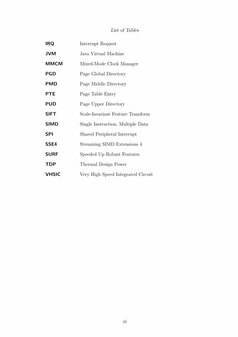
Humans visually perceive the world around them, estimating depth, rotationand speed primarily from their eyes. Current e�orts to build machines thatcan navigate and interact with the world as we do rely on more than just avideo camera. They involve much larger equipment which are often active,such as laser range finders and GPS units [13][31]. Systems which rely solelyon image based sensors are di�cult to implement in real-time on micropro-cessor based systems because of the computationally intensive nature of thealgorithms employed [11][41][49][42][12][54][15]. This project explored imple-menting a computational intense image stabilisation algorithm based aroundthe Fast Fourier Transform (FFT), the most important numerical algorithmof our lifetime [16], with the goal of gaining real-time performance.
Programmers in many applications treat the computer system as a blackbox, relying on the compiler to optimise their code for the underlying machine.In applications where performance is not critical, the development time foroptimising the code is too costly. However for real-time applications, this thesisshows that the programmer should apply optimisations that are amenable to
1
Chapter 1 Introduction
2 4 8 16 32 64 128
256
512
1024
2048
4096
8192
1638
432
768
6553
613
1072
2621
44
0
500
1,000
1,500
2,000
Transform Size
Spee
d(M
FLO
PS)
�ts�tw3-estimatejava-radix2
Figure 1.1: Performance of FFT code on an Asus Eee Pad TF201, which uses the NvidiaTegra 3 quad-core SoC. Source: [7]
the underlying machine.
Even then, software running on a microprocessor could benefit from hard-ware accelerators sharing the computational load, especially with low powereddevices such as mobile devices. Apple is a world-leader in this area, they re-leased the first 64-bit mobile processor in Q3 2013, and incorporate a lot ofcustom hardware into their chips [45], for example the Audience audio process-ing circuitry [28] was used in the iPhone 4, and also in other mobile deviceslike the Samsung Galaxy S3.
Programming languages that use virtual machines are popular among manyprogrammers. Java is an example of this, using the Java Virtual Machine(JVM) to run applications, allowing the code to easily support many systemsbecause it is always run on a virtual machine. This portability comes at a costhowever, with the overall performance of Java applications taking a huge hitdue to running virtually. Figure 1.1 compares the performance of di�erent FFTimplementations, and shows that the Java implementation cannot competewith other performance optimized solutions.
2
Chapter 1 Introduction
1.1 Hypothesis
Real-time implementation of computationally intensive image processing al-gorithms requires the application of optimisations that are amenable to theunderlying machine, with low power systems requiring further acceleration viacustomised hardware to meet power constraints. To evaluate this hypothesis,the performance of a typical C implementation of an image stabilisation algo-rithm is optimised by hand to remove common computation, use the memorysubsystem e�ciently, and use machine specific instructions on both the x86 andARM architectures. This is discussed in Section 3.2 with the results presentedin Sections 4.1.1 and 4.1.2, where the optimised code is compared to the origi-nal code. Once the algorithm has been highly optimised in software, o�oadingcomputational intense functions such as the FFT into hardware will furtherimprove the performance of the algorithm while not drastically increasing thepower usage of the device, or the overall development time. This was per-formed using a state-of-the-art Xilinx Zynq device which couples together anARM Cortex-A9 and reconfigurable logic, with the implementation discussedin Section 3.3 and results in Section 4.1.3.
1.2 Scope
The scope of this project has been limited to accommodate for the short periodof time available. With regards to the image stabilisation algorithm, the qual-ity of the output image only needs to show improvements over the input image,and can treat the input as a fixed point in space, meaning it does not have tohandle desirable movements. This is because the hypothesis is based aroundperformance, with the quality of the output just needing to remain consistent.The hardware used for performance testing was limited to technology availableat the start of the project, an early 2013 MacBook Pro, and an engineering sam-ple Xilinx Zedboard that uses a Zynq 7020. The hardware chosen for furtheracceleration was a Field-Programmable Gate Array (FPGA) because previouswork described in Section 2.2 showed the performance exceeds Graphic Pro-cessing Units (GPUs) for real-time applications. Only reprogrammable chipswere considered and not more advanced approaches such as an Application-Specific Integrated Circuit (ASIC) or a Digital Signal Processor (DSP) becauseof the time constraints.
3

2
Background
2.1 FPGAs
A Field-Programmable Gate Array (FPGA) bridges the gap between hard-ware and software, by providing performance closer to that of an Application-Specific Integrated Circuit (ASIC), while having the reconfigurability of a mi-croprocessor. They contain a finite amount of programmable logic, also knownas reconfigurable logic, that can be used to implement digital circuits by ap-plying a bitstream file to the device. This bitstream file is analogous to acompiled program in software, but where programs contain machine instruc-tions, a bitstream file contains a sequence of bits which configure circuits andlogical functions. The inner workings of a FPGA is very complex, with adetailed overall given in Reconfigurable computing: the theory and practice ofFPGA-based computation [22], however from a high level they made up of logicblocks, Input/Output (I/O) blocks, along with other built-in components suchas DSPs, MMCMs and BRAMs. Figure 2.1 shows an overview of the internalsof a FPGA.
2.2 Previous Work
There is a large body of work concerned with real-time image processing usinga Central Processing Unit (CPU) or the Graphics Processing Unit (GPU) andclaim to give real-time performance [49][42][12][54][15][41][11][47][46]. How-ever there is some work targeting FPGAs which also claims real-time perfor-
4

Chapter 2 Background
Figure 2.1: An FPGA is composed of configurable logic and I/O blocks tied togetherwith programmable interconnects. Source: [23]
mance [43][34].
2.2.1 CPU
Applications such as video surveillance need to detect moving objects, andCucchiara et al. [11] propose a system called Sakbot to do just that, whiletrying to eliminate objects shadows and ghosts caused by a moving objectsbecoming stationary for a long period of time. They accomplish this by usinga technique called background subtraction and used easy to compute methodswhich still provided good repeatability. On a Pentium 4 with a 320x240 videostream, the performance was 9-11 Frames Per Second (FPS) (ibid.).
Pattern Recognition is a common use of video processing and Ruta et al. [41]developed a two stage road sign detection and classification system. Unlikeprevious work in this area, they used colour information instead of black andwhite as colours o�er important information on a road sign. To detect a sign inthe video, they looked for shapes and rim colours. All of their 210 sign imageshad a resolution of 60x60, and with a video stream of 640x480, managed 25-30 FPS (ibid).
Google have developed a video stabilisation algorithm [20] and a camerashutter removal algorithm [19] for use on YouTube. Both of these algorithmsare computationally intense, for example they use feature extraction to detectkey points in each frame, and apply full image warps resulting in poor cachelocality. The video stabilisation algorithm on a low resolution video can reach
5

Chapter 2 Background
20 FPS, however will wobble suppression, this drops to 10 FPS. The camerashutter removal algorithm also applies video stabilisation, and is reported toget 5-10 FPS.
These are just a few examples but there is a lot of work which claims toachieve real-time performance on a CPU, with the frame rates anywhere be-tween 5-40 FPS at resolutions ranging from 240x180 to 640x480 [49][42][12][54][15].
2.2.2 GPU
The primary purpose of a GPU is to accelerate the rendering of graphics tobe displayed on a monitor, but more recently GPUs are also being utilised forgeneral purpose computing. They process many warps in parallel, with eachwarp executing the same instruction multiple times [29]. In order to maximiseperformance, GPU programmers are advised to maximise occupancy and fullysaturate the GPU with threads, however it is claimed that using thread levelparallelism and instruction level parallelism gives the best results in manycases [44].
A framework for creating abstracted video and images in real-time was de-signed in 2006 by Winnemoller et al. to be highly parallel allowing it to be runon a GPU [47]. There were 6 di�erent techniques used in this framework inwhich an image flows through before it was abstracted: feature space conver-sion, abstraction, luminance quantization, Di�erence of Gaussian (DoG) edges,colour space conversion and image based warping. Since they were focused onreal-time, they chose cheaper computation methods over more expensive ones.For a 640x480 video stream their framework managed to get 9-15 FPS on aNvidia GeForce GT 6800. They also tested it on a Athlon 64 3200+ CPU andgot 0.3-0.5 FPS (ibid.).
Digital Matting is where the background of an image is removed leavingthe foreground object, similar to how movie sets use Green and Blue screensfor special e�ects. A real-time matting system was proposed using a Time-of-Flight camera and multichannel Poisson equations by Wang et al. [46] for theCPU and GPU. They split up the algorithm, performing tasks where flexiblelooping and branching was required on the CPU, and optimized parts to beparallel to take advantage of the GPU. Using a 320x240 video stream, overallthey managed to achieve 32 FPS, however 70% of this computation in termsof runtime, was spent on the CPU (ibid.).
6

Chapter 2 Background
In summary, highly parallel algorithms may achieve high throughput ona GPU, but because GPUs have limited gather-operation capabilities [47],limited bus bandwidth, plus CPU and memory bottlenecks when transferringdata/control between the CPU and GPU, the overall runtime can be up to50x longer than the time taken for the GPU to compute the result [18]. It hasalso been claimed that GPUs o�er 100x the performance of CPUs but othermore comprehensive studies put that figure at about 2.5x on average [29].
2.2.3 FPGA
Edge detection algorithms have been implemented within a FPGA such asCanny Edge Detection [34] and the Sobel operator [43]. Canny Edge detectioninvolves Gaussian blurring/smoothing, finding derivatives of Gaussian images,non-maximal suppression and hysteresis thresholding which is more compli-cated than Sobel, where the main computation is applying two 3x3 kernelsto the image. The Canny implementation runs at 264MHz and manages toprocess over 4000 FPS for a 256x256 frame size. The Sobel implementationmanaged to get 50 FPS with a frame size of 750x576 running at 27MHz. Eventhough Canny Edge detection involves more computation, it was faster thanSobel. The authors of the Sobel implementation mention that if they addedmore pipeline stages into their design, it would be able run at a lot higher fre-quency, but the main reason the Canny design is so fast is because they useda line bu�ering technique. In summary, the performance of FPGAs exceedsthat of GPUs and CPUs for image processing, which is why they were chosenfor this project.
2.3 Image Stabilisation Techniques
Image stabilization algorithms try to eliminate rotation di�erences betweenframes while also removing unwanted x y translations. For a human to comparetwo images and figure out the rotation and translation di�erence is fairly trivialin most cases, however for a machine to do so is non-trivial. Most of thecurrent solutions for finding the rotation and translation between two frameseither use a key point feature extraction algorithm [5][20], or use sensor datafrom gyroscopes [27]. Using data from gyroscopes limits the use cases, sincenot all devices have gyroscopes, and it makes post-processing more di�cultbecause the gyroscope data would need to be encoded with the video. So even
7
Chapter 2 Background
though using gyroscope data would give accurate rotation between frames, itis not a solution that can be widely applied.
There are two main algorithms for key point feature extraction, Scale-Invariant Feature Transform (SIFT) and Speeded Up Robust Features (SURF).These work by trying to find points in an image which are unique comparedto other points around it. To find the rotation between two frames involvescomparing the key point describers and finding matching points between thetwo frames. The matching points x y values then can be used to find therotation and translation between the two frames. Using key points for findingthe rotation works well and is widely used but there are many cases when itcan struggle, for example if there are not many key points, or too many similarkey points. They are also heavily e�ected by moving objects in the scene sincethese objects would contain key points.
There is not often going to be a huge di�erence between two neighbouringframes, because they are only 1/30th of a second apart (30 FPS), but it alldepends on how close the objects are to the video camera. For example videofootage from a drone is going to contain objects far away from the cameraso the di�erence between the neighbouring frames is not going to be thatgreat. However using a smart phones front facing video camera involves havingyour face very close, so any movements can cause bigger di�erences betweenframes than the drone. Because this application is being designed more for adrone type device, two neighbouring frames are going to be similar. Insteadof using an algorithm that has been widely used for video stabilization, likekey point feature extraction, this project is going to explore the use of a FastFourier Transform (FFT) based algorithm which is used for automatic imageregistration [39][50].
This type of algorithm can find the rotation and translation between twoimages which share a lot of the same content and is used in applications whereimages need to be stitched together, like panorama or large aerial photos. Onereason why this type of algorithm might not be used for video stabilization isthat it is computationally expensive, however since this will be implementedpartially in hardware, this should not be a big concern. Also doing this ap-proach in hardware will be much easier than an approach using feature extrac-tion because if the camera resolution is known, then the hardware design canbe static. Unlike if a feature extraction approach was used, it would have to
8

Chapter 2 Background
deal with x number of features and try to match them in a dynamically sizedtree. Also the initial testing of feature extraction using a custom and libraryimplementation of SURF, did not give positive results. Using an artificiallyrotated image, the angle returned was not very accurate, which is not idealsince it is been used for stabilization. Then the fact both SIFT and SURFhave patents, meant using one of them could have been challenging.
9
3
Implementation
“People who are really serious about softwareshould make their own hardware”
— Alan Kay
This chapter describes the implementation of the image stabilisation algo-rithm in software and hardware, and has been split into four parts: algorithmoverview, software implementation, hardware implementation, and integration.The algorithm overview describes how the algorithm in this project works, andthe baseline implementation. Software details the improvements and optimi-sations made to the baseline implementation on x86 and ARM. The hardwaresection details the implementation of a Fast Fourier Transform (FFT) modulein reconfigurable logic, and integration explains how the software and hardwarewere connected together so that they could communicate with each other.
3.1 Image Stabilisation Algorithm
The image stabilisation algorithm implemented and optimised in this projectwill be described to gain an appreciation on how computationally intense itis. First, the baseline implementation will be described, then the two intensetransforms used, the Fast Fourier Transform (FFT) and Log Polar transformwill be explained. Lastly how the algorithm finds the translation and rotationwill be described, with the algorithms execution flow shown in Figure 3.6.
10
Chapter 3 Implementation
3.1.1 Baseline
The first implementation of the Image Stabilisation algorithm was written inC and is based on the frequency-domain based algorithms described in [50]and [40]. For computing the seven 2D FFTs originally needed for this al-gorithm, the highly optimised The Fastest Fourier Transform in the South(FFTS) library [9] was chosen because it reports better performance thanother optimised solutions, supports the C language, and both the x86 andARM architectures. This first implementation was never about making thecode tidy or e�cient, it was to test that the algorithm will be able to correctlyfind the angle and translation between two neighbouring frames.
This implementation first converts the input image from FFmpeg [38] to grayscale, and reduces the size of the image in memory by one third. Currently,the output is still gray scale but it would be possible to bu�er the colourimage, and correct it once the rotation and translation values are known.Originally the algorithm was producing accurate outputs when tested on afew images, with the second being artificially rotated and translated, so thatthe result values were known. However it was having problems with imagesthat were slightly blurry or with little gray scale variance, for example a close-up of a tree. To solve this, the Scharr Sobel edge detector was used in apreprocessing step to find the outlines of objects, which made the image morecrisp while also reducing the amount of data that could a�ect the result. Thisimproved the rotation and translation calculations quite significantly and madethe algorithm more robust when working with noisy or out-of-focus images.
3.1.2 Fast Fourier Transform
The FFT is an algorithm used to speed up the computation of discrete Fouriertransforms. These transforms convert time and space into the frequency do-main and vice versa. The basic idea of a Fourier transform is given an object,using filters it tries to find what the object is made o�. For example a radiowave is composed of many di�erent sine waves, a Fourier transform can findthe magnitude and phase of these individual sine waves from the original ra-dio wave. This image stabilization implementation needs to apply a discreteFourier transform to an image in two dimensions and find the inverse Fouriertransform. It will be using the FFTS [9] library because it is highly optimizedfor both the x86 and ARM architectures.
11

Chapter 3 Implementation
Detailed explanations on the FFT can be found here [10][8], but to gain anappreciation on how computationally intense the FFT is, computing the 1DFFT on an array with the transform size of 1024 using a radix-2 implementa-tion, takes over 50,000 floating-point operations [30]. The overall performanceof a radix-2 implementation of N operations gives O(Nlog
2
N) where 2 is theradix size. This is because each element in the array is accessed log
2
timeswhile the FFT computes the two-point transform, then the four-point trans-form, through to the Nth-point transform, which also results in poor tempo-rally locality. Sample code that was written and tested during this project isshown in Appendix A.1. One note, the sign parameter should be ≠1 for a 1DFFT and 1 for the inverse 1D FFT.
The 2D FFT of an array with a size of NxN can be decomposed into 2N 1DFFTs. The first step is to compute the 1D FFT for each row in the 2D array,then the 1D FFT needs to be computed for every column of the results fromthe first step. This results in poor spacial locality, hindering the performanceof the 2D FFT even more. Instead of computing on the columns, the array canbe transposed allowing rows to be computed again, but this is only a slightimprovement.
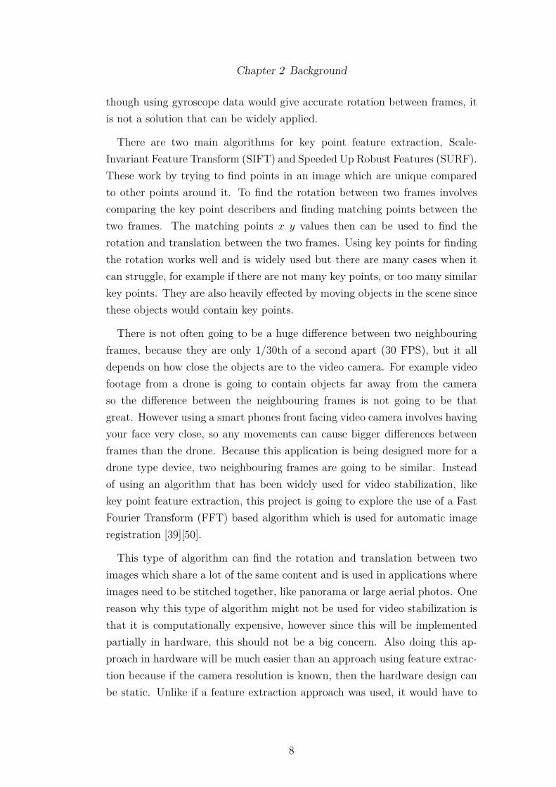
An example of the 2D FFT being applied to a couple of images is shown inFigure 3.1 and Figure 3.2. The images in Figure 3.1 show cropped images ofa model car with Figure 3.1b artificially rotated by 10 degrees. Then the 2DFFT was computed for both images and represented in a modulus form shownin Figure 3.2, resulting in galaxy like images. These two modulus images lookvery similar, however focusing on the two main lines that cross through thecenter point of both images, the line in Figure 3.2b seems slightly rotated. It isactually rotated by 10 degrees, the same as the image in Figure 3.1b. Thus the2D FFT can provide very useful information that can be used for applicationslike image stabilization, however this is not actually how the rotation is found,it is just an example.
3.1.3 Log Polar Transform
The Log Polar transform is critical for the algorithm to find the angle di�erencebetween two images. It is similar to the Polar transform, where it warps animage around the center point, by converting the Cartesian coordinates fromthe input image to Polar coordinates for the output [3]. An example of the Log
12

Chapter 3 Implementation
(a) 0 Degrees Rotation (b) 10 Degrees Rotation
Figure 3.1: Gray scale images of a model car.
(a) 0 Degrees Rotation (b) 10 Degrees Rotation
Figure 3.2: Modulus images of the computed 2D FFT for both images in Figure 3.1.
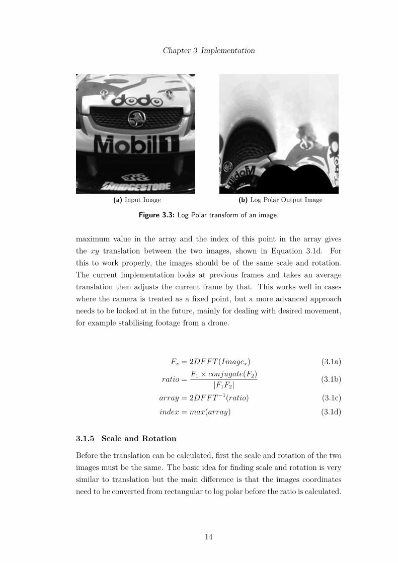
Polar transform is shown in Figure 3.3, with the input image in Figure 3.3a andthe output image in Figure 3.3b. The output has the original image warped insuch a way that every angle exists within it, and it is this property that allowsthe angle between two images to be found, by finding the strongest match forsecond image in the Log Polar output.
3.1.4 Translation
Using the Fourier transform to find the translation between two images relieson the Fourier Shift theorem. This states that the phase of a defined ratiois equal to the phase di�erence between two images. Therefore to find thetranslation, first the ratio must be computed, as shown in Equation 3.1b,and then the inverse Fourier transform is applied to the ratio as shown inEquation 3.1c which will result in an array of numbers. Most of these numberswill be zero apart from a small region around a point. This point will be the
13
Chapter 3 Implementation
(a) Input Image (b) Log Polar Output Image
Figure 3.3: Log Polar transform of an image.
maximum value in the array and the index of this point in the array givesthe xy translation between the two images, shown in Equation 3.1d. Forthis to work properly, the images should be of the same scale and rotation.The current implementation looks at previous frames and takes an averagetranslation then adjusts the current frame by that. This works well in caseswhere the camera is treated as a fixed point, but a more advanced approachneeds to be looked at in the future, mainly for dealing with desired movement,for example stabilising footage from a drone.
F
x
= 2DFFT (Image
x
) (3.1a)
ratio = F
1
◊ conjugate(F2
)|F
1
F
2
| (3.1b)
array = 2DFFT
≠1(ratio) (3.1c)index = max(array) (3.1d)
3.1.5 Scale and Rotation
Before the translation can be calculated, first the scale and rotation of the twoimages must be the same. The basic idea for finding scale and rotation is verysimilar to translation but the main di�erence is that the images coordinatesneed to be converted from rectangular to log polar before the ratio is calculated.
14
Chapter 3 Implementation
The first step is to compute the 2D FFT of both images and then compute theabsolute values of the complex numbers, shown in Equation 3.2a. A highpassfilter is applied to remove any low frequency noise before the log polar valuesare computed, as shown in Equation 3.2b, then the 2D FFT is applied again.The ratio and index is then computed the same as it was in Equations 3.1b, 3.1cand 3.1d. However this time the index finds the angle and scale values. Thisis shown in Equation 3.3 and Equation 3.4 assuming the index value is for a1D array. Currently the scale is not being corrected since neighbouring framesshould already have a very similar scale, however this is an area which can beexplored in the future.
Fa
x
= abs(2DFFT (Image
x
)) (3.2a)Flp
x
= logpolar(highpass(Fa
x
)) (3.2b)F
x
= 2DFFT (Flp
x
) (3.2c)
angle = (180 ◊ index)/(height ◊ width) (3.3)
b = 10log10(width)/width
scale = b
index mod height
(3.4)
15
Chapter 3 Implementation
3.2 Software
3.2.1 Locality
Once a baseline implementation was established, the code was rewritten fromscratch to make e�cient use of the machines cache. Cache access has lowerlatency than main memory, which reduces stalls when accessing memory withpoor locality [25]. Memory locality can be broadly divided into two types:temporal and spatial locality
Temporal locality is where data is reused within a short period of time andheavily applies to loops, where a section of memory is read, processed andstored, and then repeated in a short amount of time. During the processingstage, the cache is being used, and the other two stages involve using thephysical memory. So therefore for the best performance, as much computationon a section of data that can be performed at once should be combined intoone loop. For example, applying the Sobel filter, normalising and convertingthe data to a complex number, is all performed in a single loop instead ofthree. This reduces the memory access by approximately two thirds becausethe cache is being fully utilised. All the functions in between the FFTs wereable to be combined into one function apart from the Log Polar transform,which will be explained later.
The idea behind spatial locality is that if you access something once, you arelikely to use its neighbour. For example an address in memory has just been ac-cessed, the likelihood of the next address being a neighbouring address is high.Therefore there is a better chance of the address being in a cache line, reduc-ing the amount of cache misses and in turn the amount of physical memoryaccess, increasing the overall performance. The standard row-column methodof computing the 2D FFT has poor spatial locality because it accesses columnsof the array, where the FFTS library transposes the data when the columnsare required to improve spatial locality. Another function in this algorithmwith poor spatial locality is the Log Polar transform. It reads data sequen-tially, but because of the nature of the transform, where it is wrapping thedata around itself, the output data is non-sequential giving very poor spatiallocality, which like the 2D FFT, is di�cult to avoid. The remaining functionshave good spatial locality because they access and store data sequentially.
16

Chapter 3 Implementation
3.2.2 Common Computation
This algorithm will be computed over many frames, so factoring out computa-tion between frames can increase performance. The computation time for theLog Polar transform was greatly improved by only computing the output in-dices once, and reusing the indices for every frame by storing them in an array.This improved performance because each output index requires the comput-ing of computationally intense power and trigonometric functions [26]. Thistakes more instructions and CPU time to compute than fetching the indexfrom cache or memory. However this approach cannot be applied to all com-putations, there is a trade o� storing pre-computed results in memory becauseof the access time, so even if a few instructions are common (give the sameoutput), computing them each time can actually still be faster than gettingthem from memory.
When computing the algorithm on the current frame, the previous framerequires a lot of computation to be able to compare the two frames. Howeverthe previous frame has already been through all the computation required,meaning there is no point in doing it again. Therefore during stages of thealgorithm, the current frames frequency representation is cached, so it can beused when comparing against the next frame. This reduces the number of2D FFTs from seven to five, along with reducing the use of other functions.Bu�ering the previous frames data does have a small cost though, the angle andtranslation values are now computed with the unfiltered previous frame insteadof the filtered one. This means all the previous values need to be combinedso the current angle and translations are known, which does not a�ect theperformance, however the quality of the output can be slightly impacted insome cases with regards to translation.
3.2.3 Intrinsics
Modern CPUs have a hardwired performance increasing technique which pro-grammers can take advantage of called vector intrinsics. Intrinsics are simplya way of utilising low-level instructions without having to use assembly, be-cause supported compilers have intimate knowledge of them. These intrinsicsallow the same instruction to be computed on multiple words in a single cycle,thus greatly reducing the amount of instructions the CPU has to execute. Thedownside of using intrinsics is that it makes the code far less portable across
17

Chapter 3 Implementation
multiple architectures, and even CPU versions because they are very hardwarespecific. To solve this problem, C macros were used within the code so thedi�erent intrinsics can be swapped out by simpling changing a header file, andcompiler macros to allow di�erent versions of code to be built depending onthe available intrinsics.
As with writing the functions to have good cache locality, not all functionscan be improved with intrinsics, it is possible to actually make a function haveworse performance than using single instructions. A vector of size N doesnot give N times the performance for a function, especially when dealing withcomplex numbers and pixel data where the data is interleaved, because gettingthe data into the correct positions in the vectors is not always easy, and canresult in needing more instructions than without intrinsics. Once again theLog Polar transform was a good example of this, because of its non sequentialoutput, using intrinsics did not improve performance, but instead made itworse.
Intel SSE4 and AVX
On Intel, Streaming SIMD Extensions 4 (SSE4) and Advanced Vector Exten-sions (AVX) were the first to be implemented in this project, and supports awidth of 256 bits allowing for 8x32bit floating points to be executed in paral-lel. This version does not support stride loads or stores, also known as vectorscatter/gather, which allows memory to be accessed using a step size, for ex-ample to fill a vector of red values from a RGB pixel array would require astep size of three and only one instruction. Therefore getting the complexnumbers into the correct format using SSE4 involved using shu�es, blends,permutes, and unpacking high and low words. The other issue was that the256 bits is actually made up of two 128 bits lanes, meaning data in one lanecould not be easily moved to the other, which often meant that a vector ofthe real or imaginary parts was not able to be in sequence. One example onsplitting a complex number into its parts is shown in Figure 3.4, which loads2 vectors and using the shu�e function to extract the parts. The shu�e maskfor the real vector is 1000100010001000
2
and each pair of bits choses whichword should go into the output vector. The upper 4 bits 1000
2
translates tothe 0th and 2nd word in the first vectors upper 128 bits. Then the next 1000
2
selects the 0th and 2nd word from the second vectors upper 128 bits. Thisrepeats for the lower 128 bits, or the other lane for both vectors and results in
18

Chapter 3 Implementation
# define _VEC_COUNT 8# define __VEC __m256# define _VEC_FLOAT_LOAD (a,os) _mm256_load_ps (a +
os)# define _VEC_FLOAT_SHUFFLE (a,b,mask) _mm256_shuffle_ps (a,
b,mask)
__VEC v0 , v1 , re , im;v0 = _VEC_FLOAT_LOAD (input , index);v1 = _VEC_FLOAT_LOAD (input , index + _VEC_COUNT );re = _VEC_FLOAT_SHUFFLE (v0 , v1 , 34952) ;im = _VEC_FLOAT_SHUFFLE (v0 , v1 , 56797) ;
Figure 3.4: Splitting complex number into parts using SSE4.
the real vector containing {R0
, R1
, R4
, R5
, R2
, R3
, R6
, R7
}. So SSE4 is notstraight forward and involves a lot of knowledge to be able to use e�ciently. Tohelp with this problem, the latest Intel family, Haswell, added a new micro-architecture Advanced Vector Extensions 2 (AVX2), which supports gatherand scatter operations that allow a complex number to be easily split into areal and imaginary vectors. However this has not been used in this projectdue to the available hardware not supporting it.
ARM NEON
The ARM NEON general-purpose Single Instruction, Multiple Data (SIMD)engine supports computing an instruction on 4x32 bit floating point values inparallel, half that of Intel, but allows stride load and store operations up toa stride length of four. Therefore splitting a complex number into the realand imaginary parts on NEON involves using the single “vld2q f32” instruc-tion, where the 2 is the stride length, and loads data into a “float32x4x2 t”type. This contains two 4x32 bit vectors, with the data loaded alternatelyinto each vector, resulting in one containing the real parts and the other theimaginary parts. AVX requires 4 instructions to process 8 complex numbers,where NEON only uses one instruction to process 4 complex numbers, whichappears to be better but with the raw performance Intel has over ARM, us-ing AVX is still faster. An interesting feature in NEON is that it does nothave a divide intrinsic, instead it allows the result to be refined depending onthe accuracy required using the Newton-Raphson method for finding betterapproximates shown in Figure 3.5, so it gives the programmer more choice
19
Chapter 3 Implementation
between performance and accuracy.
# define _VEC_FLOAT_DIV (a,b) vec_neon_div (a,b);inline float32x4_t vec_neon_div ( float32x4_t a,
float32x4_t b) {float32x4_t reciprocal = vrecpeq_f32 (b);reciprocal = vmulq_f32 ( vrecpsq_f32 (b, reciprocal )
, reciprocal );reciprocal = vmulq_f32 ( vrecpsq_f32 (b, reciprocal )
, reciprocal );return vmulq_f32 (a, reciprocal );
}
Figure 3.5: Dividing floats in Neon.
3.2.4 Optimised Flow Diagram
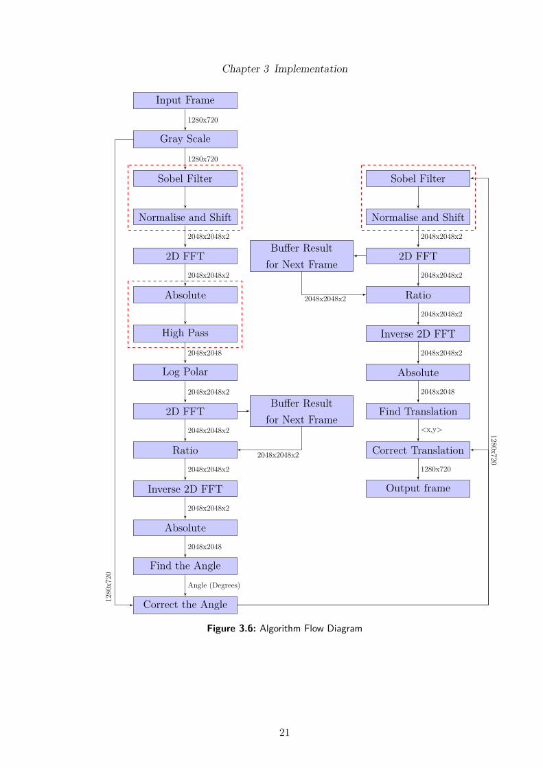
The optimised image stabilisation algorithm is shown in Figure 3.6, with anycombined functions grouped by red boxes, and the arrows are labeled with theoutput from the last function into the input of the next function. Most ofthese arrows show the array size at that point to get across how much memoryis required for this algorithm. The 2048x248x2 size means a complex numberarray of size 2048x2048. This optimised algorithm only uses five 2D FFTsbecause it is bu�ering results from the previous frame, which is less than other2D FFT image stabilisation approaches [50] [32]. The reason that the originalimage is corrected for the angle then fed through the Sobel filter again, is forfuture work to fix the missing parts of the image after it has been rotated bylooking at other frames, and also the Sobel, Normalise and Shift function isnot very computational intense.
20
Chapter 3 Implementation
Input Frame
Gray Scale
Sobel Filter
Normalise and Shift
2D FFT
Absolute
High Pass
Log Polar
2D FFTBu�er Result
for Next Frame
Ratio
Inverse 2D FFT
Absolute
Find the Angle
Correct the Angle
Sobel Filter
Normalise and Shift
2D FFTBu�er Result
for Next Frame
Ratio
Inverse 2D FFT
Absolute
Find Translation
Correct Translation
Output frame
1280x720
1280x720
2048x2048x2
2048x2048x2
2048x2048
2048x2048x2
2048x2048x2
2048x2048x2
2048x2048x2
2048x2048x2
2048x2048
Angle (Degrees)
1280
x720
1280x720
2048x2048x2
2048x2048x2
2048x2048x2
2048x2048x2
2048x2048x2
2048x2048
<x,y>
1280x720
Figure 3.6: Algorithm Flow Diagram
21
Chapter 3 Implementation
3.3 Hardware
3.3.1 Xilinx Zedboard
The platform chosen for this project was the Xilinx Zedboard, which is pop-ulated with a device integrating a dual core ARM Cortex-A9 and an Artix7 Field-Programmable Gate Array (FPGA) into the same die as the Zynq7020, allowing for the communication between the processing system and re-configurable logic to have low latency. The 28 nm chip is the first of its kindand the actual board that was used is an engineering sample, with produc-tion grade boards only becoming to be available in Q4 2013. There was littledocumentation and examples available, so many issues had to be solved withdebugging.
3.3.2 Hardware Descriptive Language
A Hardware Description Language (HDL) is used to describe the structure,design and overall operation of electronic circuits. The most commonly usedHDLs in industry are Verilog [14] and Very High Speed Integrated Circuit(VHSIC) HDL [21], with VHDL used in this project. The U.S Department ofDefense (DoD) originally developed VHDL in 1981 because they were in needof something to document the behaviour of Application-Specific IntegratedCircuit (ASIC) components. At the time the DoD were using the Ada pro-gramming language which meant VHDL had to be syntacticly similar to avoidthe need to recreate concepts, resulting in VHDL being heavily based o� Adawith regards to concepts and syntax. VHDL was later transfered to Instituteof Electrical and Electronic Engineers (IEEE) who finalised a standard in 1987,called VHDL-87. There have been many revisions and improvements to VHDLover the years with the most recent in 2008.
3.3.3 Vivado
This project evaluated the new Xilinx Vivado Design Suite for developing andbuilding projects for the Xilinx Zedboard. Victor Peng, the Senior Vice Pres-ident of Programmable Platforms Group at Xilinx, claims “the design suitewill provide a 4x boost to productivity and attacks the major bottlenecks inprogrammable systems integration and implementation. We believe it will dra-matically boost customer productivity”. This is a bold statement, and withoutknowing what development stages and design suites Peng used to get the 4x
22
Chapter 3 Implementation
boost, it is hard to verify, but as this report shows in the discussion section,there is definitely an improvement in the overall productivity for getting adesign from the planning stage to the implementation stage.
Unification
In the previous Xilinx suite, there were a number of separate programs toperform di�erent tasks, however with Vivado, Xilinx have combined most ofthese into one tool. This made designing a project much easier because therewas not the need to open di�erent applications, to do perform tasks on thesame design, which often caused errors, especially with mismatched deviceconfigurations. In saying that, Vivado has a huge number of bugs, most ofwhich are connected to the graphical interface, so it is fair from perfect at thisstage.
Simulation
When designing and building HDL projects, simulation is a quick way to verifyif a design works, and makes it easy to find errors by analysing waveforms. Asimulation tool is directly built into Vivado but it is recommended to use amore advanced tool, for example ModelSim by Mentor Graphics, because itcan more accurately simulate the logic. However for this project, simulationwas not used heavily due to most of the components needing to interact withthe hardwired components on the Zedboard, which simulation tools cannotsimulate accurately. Some HDL components were briefly tested with ModelSimjust to make sure they were behaving in the correct manor, but they still neededto be primarily tested on the physical board.
Debugging
Testing designs on the physical board is easy, unless something goes wrong.Unlike software based programs, where it is simple to use debugging toolsor by using the fprintf statement, hardware does not have an easy methodof debugging. The eight LEDs on the Zedboard can be used like a fprintfstatement, and can debug small issues, but this method is very limited and timeconsuming. Instead a debug core has to be added to the design, then connectedto the required signals and clocks to be able to take a snapshot of them when acondition is true. Before Vivado, this involved a tool to add the debug core andto connect up the signals, then another tool to program the device and setup
23
Chapter 3 Implementation
the capture condition, before being able to view the waveforms. The worstpart of this process was that the signal names were removed, so another filehad to be imported into the waveform viewer to actually know which signalswere which.
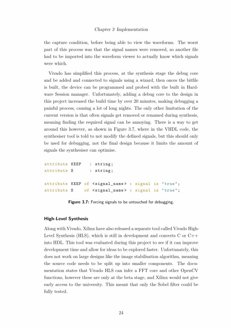
Vivado has simplified this process, at the synthesis stage the debug coreand be added and connected to signals using a wizard, then onces the bitfileis built, the device can be programmed and probed with the built in Hard-ware Session manager. Unfortunately, adding a debug core to the design inthis project increased the build time by over 20 minutes, making debugging apainful process, causing a lot of long nights. The only other limitation of thecurrent version is that often signals get removed or renamed during synthesis,meaning finding the required signal can be annoying. There is a way to getaround this however, as shown in Figure 3.7, where in the VHDL code, thesynthesiser tool is told to not modify the defined signals, but this should onlybe used for debugging, not the final design because it limits the amount ofsignals the synthesiser can optimise.
attribute KEEP : string ;attribute S : string ;
attribute KEEP of <signal_name > : signal is "true";attribute S of <signal_name > : signal is "true";
Figure 3.7: Forcing signals to be untouched for debugging.
High-Level Synthesis
Along with Vivado, Xilinx have also released a separate tool called Vivado High-Level Synthesis (HLS), which is still in development and converts C or C++into HDL. This tool was evaluated during this project to see if it can improvedevelopment time and allow for ideas to be explored faster. Unfortunately, thisdoes not work on large designs like the image stabilisation algorithm, meaningthe source code needs to be split up into smaller components. The docu-mentation states that Vivado HLS can infer a FFT core and other OpenCVfunctions, however these are only at the beta stage, and Xilinx would not giveearly access to the university. This meant that only the Sobel filter could befully tested.
24
Chapter 3 Implementation
When writing the Sobel filter in software, the naive approach is to applythe 3x3 kernel to the array directly while looping over it. However whentranslating this to hardware, the HDL produced is very ine�cient because theimage has to be stored in block ram, meaning only one value can be accessedeach clock cycle. To solve this the C code must be written with hardwarein mind, so in this case the data should be thought of as streaming throughthe Sobel filter, instead of looping over the memory. Then since each pixelrequires its neighbours, as the pixels are stream in, they need to go into adelay bu�er until they are required. When this is converted to HDL it ismuch more e�cient, with the number of clock cycles equaling the number ofpixels plus the delay bu�ers size. Therefore for Vivado HLS to produce goodHDL, the input source code must be written by a someone with knowledge ofhardware, which probably means they would prefer to write directory in HDL,so for this tool to be widely used, it needs to become smarter so standardsoftware programmers can produce e�cient HDL.
3.3.4 DDR3 AXI Interface
The reconfigurable logic on the Zedboard has 140 36Kb Block RAM (BRAM)resources [53], with 560 KB of space available in total. When dealing with largeimages, a lot of space is required to bu�er one entire image, and the BRAMresources are not dense enough. For example, a grey scale image (using abyte per pixel) with the resolution of 2048x2048, would use a total of 4MBworth of space. This means the reconfigurable logic would only be able tostore a couple of rows of the image in each block RAM at a given time, andin total approximately 1/6th of the full image. Streaming algorithms, like astandard 3x3 Sobel filter, do not have a problem with this limitation. But foralgorithms like the 2D FFT, which require the entire image, other techniquesmust be considered. This means o� chip storage is required to bu�er imagesand other large pieces of data.
On the Zedboard there are two DDR3 components that each have 256MBsof space and a data width of 16 bits. These are combined into one DDR3interface within the built-in memory controller, giving a total of 512MB ofspace and a data width of 32 bits. The processing system has full controlover the built-in memory controller, and the reconfigurable logic has four highperformance Advanced eXtensible Interface (AXI) 3 slave ports for reading andwriting to the DDR3 memory. The current design needs the processing system
25

Chapter 3 Implementation
to initialise the memory controller, whether it is on boot or by a bare metalZynq application, because if it is not enabled by software, the reconfigurablelogic cannot access memory properly. This resulted in days worth of debuggingbecause it appeared to working, the data was being read correctly, but a fewof the control signals from the memory controller never changed when theyshould have.
The high performance AXI 3 ports allow for bursting of 16x64 bit wordswhich increases performance. This is because without bursting mode, a num-ber of clock cycles are used to setup the request, 1 clock cycle to receive ortransmit the data, then finally a few more clock cycles to acknowledge thecompletion of the request, resulting in a lot of clock cycles wasted for controlsignals and just 1 for the actual data. However with bursting, the controlsignal cost remains the same, but now approximately 16 clock cycles are usedto receive or transmit the data continuously from the given address, reducingthe overall number of clock cycles needed to read or write a large amount ofdata. There is a newer version of AXI, version 4, which has been defined fora couple of years and allows bursting up to 256x64 bit words, but because theZedboard project had already been established, it was left at version 3.
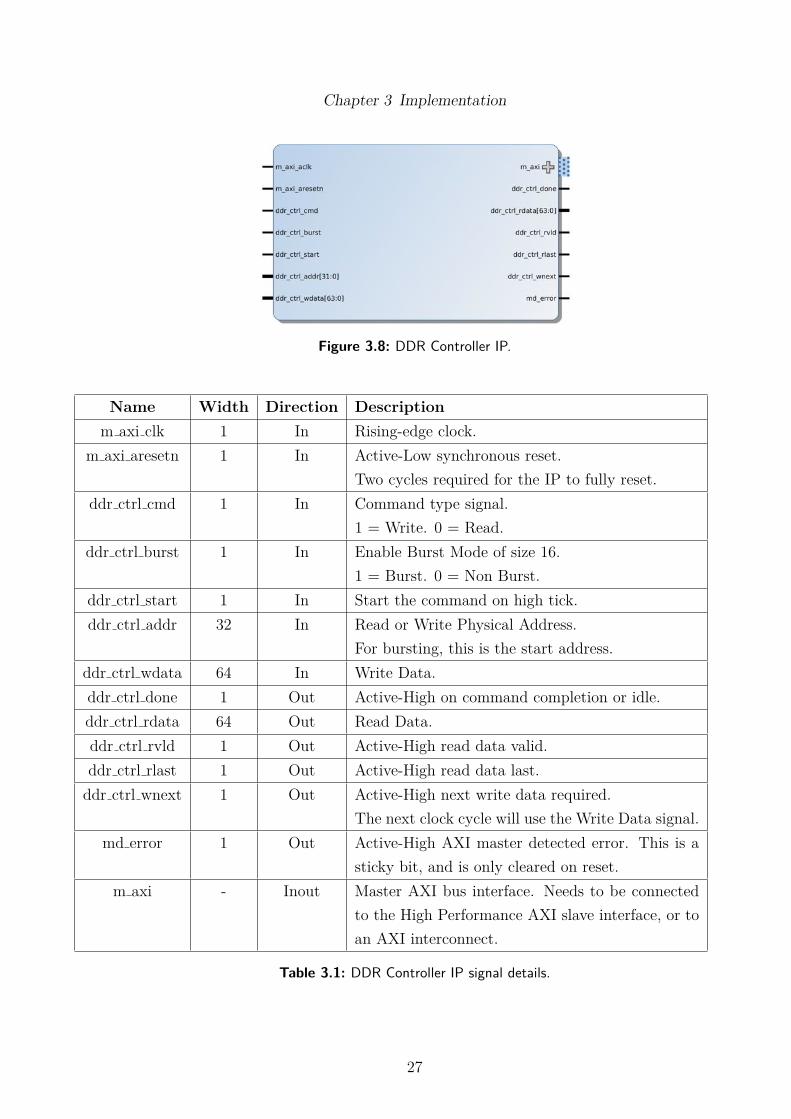
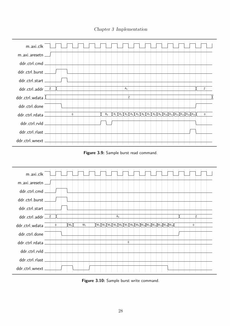
An AXI interface for the FFT IP was implemented with VHDL in thisproject and has been converted to a Vivado IP component, shown in Figure 3.8and described in Table 3.1. Creating an IP block with the AXI interfaceallows it to be connected to other components quickly using the Vivado IPIntegrator, instead of manually connecting up components which can be verytime consuming. The bulk of the VHDL is made up of many smaller componentmodules and state machines, which allow it to be more stable and support awider range of configurations. It can be used for AXI version 3 and 4 slaveports, making it more universal for other devices and includes a simple controlinterface for it to be used by other components and state machines so theycan access the DDR3 memory. Sample signals are shown in Figure 3.9 andFigure 3.10 for burst read and write respectively, the pattern of rvld and wnextcan vary but at the start of the command, there is usually a delay between thefirst and second data signal being read or written, so it is important for thesesignals to be handled appropriately.
26
Chapter 3 Implementation
Figure 3.8: DDR Controller IP.
Name Width Direction Descriptionm axi clk 1 In Rising-edge clock.
m axi aresetn 1 In Active-Low synchronous reset.Two cycles required for the IP to fully reset.
ddr ctrl cmd 1 In Command type signal.1 = Write. 0 = Read.
ddr ctrl burst 1 In Enable Burst Mode of size 16.1 = Burst. 0 = Non Burst.
ddr ctrl start 1 In Start the command on high tick.ddr ctrl addr 32 In Read or Write Physical Address.
For bursting, this is the start address.ddr ctrl wdata 64 In Write Data.ddr ctrl done 1 Out Active-High on command completion or idle.ddr ctrl rdata 64 Out Read Data.ddr ctrl rvld 1 Out Active-High read data valid.ddr ctrl rlast 1 Out Active-High read data last.
ddr ctrl wnext 1 Out Active-High next write data required.The next clock cycle will use the Write Data signal.
md error 1 Out Active-High AXI master detected error. This is asticky bit, and is only cleared on reset.
m axi - Inout Master AXI bus interface. Needs to be connectedto the High Performance AXI slave interface, or toan AXI interconnect.
Table 3.1: DDR Controller IP signal details.
27
Chapter 3 Implementation
m axi clk
m axi aresetn
ddr ctrl cmd
ddr ctrl burst
ddr ctrl start
ddr ctrl addr Z A1 Z
ddr ctrl wdata Z
ddr ctrl done
ddr ctrl rdata 0 R0 R1 R2 R3 R4 R5 R6 R7 R8 R9 R10 R11 R12 R13 R14 R15 0
ddr ctrl rvld
ddr ctrl rlast
ddr ctrl wnext
Figure 3.9: Sample burst read command.
m axi clk
m axi aresetn
ddr ctrl cmd
ddr ctrl burst
ddr ctrl start
ddr ctrl addr Z A2 Z
ddr ctrl wdata 0 W0 W1 W2 W3 W4 W5 W6 W7 W8 W9 W10 W11 W12 W13 W14 W15 0
ddr ctrl done
ddr ctrl rdata 0
ddr ctrl rvld
ddr ctrl rlast
ddr ctrl wnext
Figure 3.10: Sample burst write command.
28
Chapter 3 Implementation
3.3.5 FFT Implementation
Implementing the entire image stabilisation algorithm in reconfigurable logicwould have been costly in terms of area and development time. It wouldtake a long time to implement each part of the algorithm in VHDL, thena controller and datapath would have to be designed and built to connectthe components together, while guaranteeing the input and output signals areworking at 30 Frames Per Second (FPS). Finally on top of all that, the toolswould not be able to fit the design into the reconfigurable logic automatically,so the design would have to be laid out by hand, which is very time consuming,and is rare in industry. An alternative approach is to only implement the FFTfunction in reconfigurable logic, with the software able to use the hardware tocompute the FFT.
Once again the time requirements of this project meant that developing aFFT core from the ground up would not have been possible, so instead theXilinx FFT Logicore [52] was used for computing the FFT. This core is highlyconfigurable, with many performance vs area options available. Because thisproject is about raw performance, the Radix-4 burst IO butterfly architec-ture [48] was selected, which allows for parallel computation, along with usinga 4-multiplier structure with the XtremeDSP slices, meaning the buttery stagesare implemented with DSPs instead of slice logic.
The core has three data buses, the configuration bus, which allows the trans-form length of the FFT to be set, then the data input and output buses. Theinput bus has four signals, a 64 bit wide data signal for the complex number,the data last signal to tell the core this is the last complex number which willstart the computation. The data valid signal is set to high when the inputdata is valid, and the last signal is the ready signal, which is an output of thecore and is used for the controller to know when the core is ready to exceptdata. The output bus has actually the same signals in the opposite direction,apart form the ready signal.
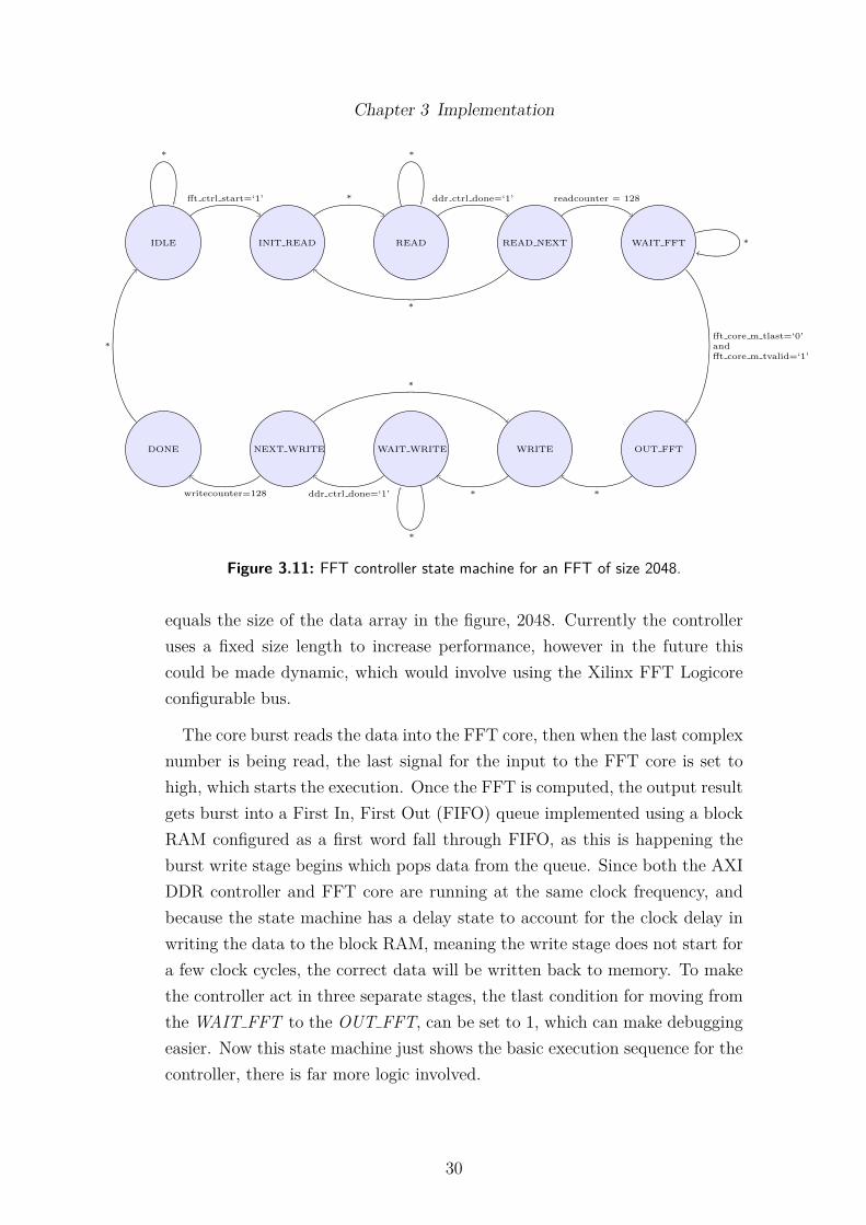
Another controller was developed to drive the FFT core and handle readingand writing data from memory using the AXI interface controller, and thestate machine for this controller is shown in Figure 3.11. Note the * charactermeans the lowest priority condition, and the current state transitions to thenext state on the rising edge of each clock cycle. The two counters that count to128 are actually counting the number of complex numbers, 128 x 16 (burst size)
29
Chapter 3 Implementation
IDLE INIT READ READ READ NEXT WAIT FFT
OUT FFTWRITEWAIT WRITENEXT WRITEDONE
*
�t ctrl start=‘1’ *
*
ddr ctrl done=‘1’ readcounter = 128
*
�t core m tlast=‘0’and�t core m tvalid=‘1’
*
**ddr ctrl done=‘1’
*
*
writecounter=128
*
Figure 3.11: FFT controller state machine for an FFT of size 2048.
equals the size of the data array in the figure, 2048. Currently the controlleruses a fixed size length to increase performance, however in the future thiscould be made dynamic, which would involve using the Xilinx FFT Logicoreconfigurable bus.
The core burst reads the data into the FFT core, then when the last complexnumber is being read, the last signal for the input to the FFT core is set tohigh, which starts the execution. Once the FFT is computed, the output resultgets burst into a First In, First Out (FIFO) queue implemented using a blockRAM configured as a first word fall through FIFO, as this is happening theburst write stage begins which pops data from the queue. Since both the AXIDDR controller and FFT core are running at the same clock frequency, andbecause the state machine has a delay state to account for the clock delay inwriting the data to the block RAM, meaning the write stage does not start fora few clock cycles, the correct data will be written back to memory. To makethe controller act in three separate stages, the tlast condition for moving fromthe WAIT FFT to the OUT FFT, can be set to 1, which can make debuggingeasier. Now this state machine just shows the basic execution sequence for thecontroller, there is far more logic involved.
30
Chapter 3 Implementation
To create a state machine within reconfigurable logic, three process blocksare required for an e�cient solution. The main process block is driven by achange in state, and defines what signals should be set too for each state. Thisinvolves one large case statement, and it is important to include all the signalsthat any state requires, to get the tools to infer the state machine correctly.Quite often some states do not actually set any signals, they are just used asa clock delay, or wait for a condition to occur, like the WAIT FFT state inFigure 3.11. Using the when others case allows for a default state to be used,which can make the case statement cleaner and reduces the amount of time todevelop and modify the state machine.
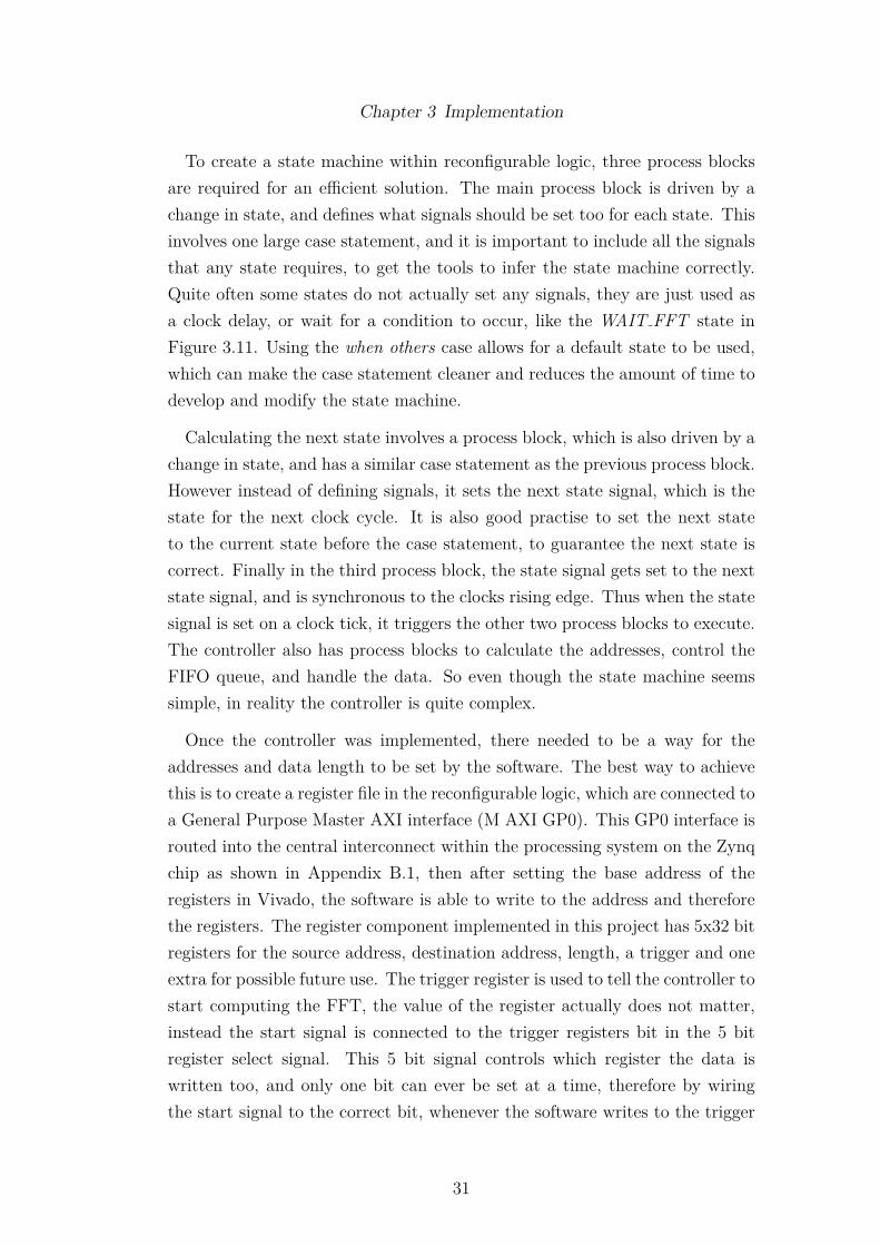
Calculating the next state involves a process block, which is also driven by achange in state, and has a similar case statement as the previous process block.However instead of defining signals, it sets the next state signal, which is thestate for the next clock cycle. It is also good practise to set the next stateto the current state before the case statement, to guarantee the next state iscorrect. Finally in the third process block, the state signal gets set to the nextstate signal, and is synchronous to the clocks rising edge. Thus when the statesignal is set on a clock tick, it triggers the other two process blocks to execute.The controller also has process blocks to calculate the addresses, control theFIFO queue, and handle the data. So even though the state machine seemssimple, in reality the controller is quite complex.
Once the controller was implemented, there needed to be a way for theaddresses and data length to be set by the software. The best way to achievethis is to create a register file in the reconfigurable logic, which are connected toa General Purpose Master AXI interface (M AXI GP0). This GP0 interface isrouted into the central interconnect within the processing system on the Zynqchip as shown in Appendix B.1, then after setting the base address of theregisters in Vivado, the software is able to write to the address and thereforethe registers. The register component implemented in this project has 5x32 bitregisters for the source address, destination address, length, a trigger and oneextra for possible future use. The trigger register is used to tell the controller tostart computing the FFT, the value of the register actually does not matter,instead the start signal is connected to the trigger registers bit in the 5 bitregister select signal. This 5 bit signal controls which register the data iswritten too, and only one bit can ever be set at a time, therefore by wiringthe start signal to the correct bit, whenever the software writes to the trigger
31
Chapter 3 Implementation
register, the FFT will be computed. But when the computation is finished,the software needs to know so it can continue executing. The spare registercould be used so that the software reads from it checking for a completion flag,however this would require constant polling and would a�ect performance. Soinstead an interrupt signal is used because it allows the software to be notifiedinstantly, and very little extra computation on the software side. The registerfile component handles this interrupt, and has an output signal defined as aninterrupt signal that is connected to the Interrupt Request (IRQ) handler onthe processing system, shown in Appendix B.1. Also from within this windowthe IRQ number can be set, which will be needed for the integration section.
There have been three components created in this project and have beenconverted into Vivado IPs, using the IP packager allow them to be added to theVivado IP Integrator tool: an AXI DDR3 controller, FFT controller and FFTconfiguration component. These IPs were connected together, along with otherstandard IPs, to create the overall design, which is shown in Appendix B.2. TheZynq Processing System has two external buses for other I/O and the DDR3bus, with the pins defined in a default design constraints file for the Zedboard.Two of the output pins of the Processing System, drive the reconfigurablelogic, the not reset signal which is connect to the reset IP, and the fixed100MHz clock signal. In order for a faster clock to be used in the reconfigurablelogic, the 100MHz signal must be inputted in a Mixed-Mode Clock Manager(MMCM) [51], which is a built-in resource and is found in a clock managementtile, and allows for the generation of di�erent clock frequencies and phases. Thedesign is currently running at 165MHz, with faster speeds possible however itis failing timing and finding the part which is causing the issue is not easy,even with the tools supposedly reporting whereabouts the problem is.
When the design has been run through synthesis and place and route, afloor plan of the design is produced shown in Appendix B.3 which visualisesthe implemented design on the actual die. The floor plan makes it clear howmuch area is required just to compute the FFT, which is represented by theaqua colour, and the amount of area for all the other logic involved just tocontrol the design.
32
Chapter 3 Implementation
3.4 Integration
The operating system used in this project was Linaro 13.04, which has been de-signed for the ARM architecture by Linaro, a non-profit organization [1]. Thisoperating system is fully open source which allowed the Zedboard communityto make modification in order to get it running. There are many tutorialsavailable online that supposedly document the process to get Linaro running,however few work and those that do still require further changes to work prop-erly. A lot of very important details were missing from these tutorials, likethe actual boot sequence, device trees, U-Boot customisations and how to goabout making changes to the Linux kernel. This section summarises these dif-ferences while describing the process of communicating with custom hardwareon the Zedboard.
3.4.1 Boot Process
Understanding how a Linux kernel boots on the Zedboard is critical, because itis during this stage that all the customization in the reconfigurable logic andkernel takes e�ect. A factory programmed ROM is responsible for the firststage of the boot process and this cannot be edited by the user. This stagepartially initializes the system and performs some checks, including determin-ing which device to boot from based on the jumper settings, with the jumpersettings for booting from the SD card described in Table 3.2.
There needs to be at least two partitions on the SD card, the first needs tobe approximately 40MB in size and is used primarily for the boot process. Thesecond can be the size of the left over space and is used for the file system if theoperating system needs one. On the boot partition, needs to be a First-StageBoot Loader (FSBL) file which the ROM program will execute. This FSBL fileis combined into a binary file with the reconfigurable logic definition file (.bit)and then a U-Boot executable file. So straight after the FSBL gets executed,the reconfigurable logic gets configured before the Zedboard tries to load anoperating system. The reason the reconfigurable logic has to be configuredsecond is because it can contain important devices such as graphics and audiothat the operating system requires.
33

Chapter 3 Implementation
Jumper Mode ConnectionJP7 Mode0 GNDJP8 Mode1 GNDJP9 Mode2 3V3JP10 Mode3 3V3JP11 Mode4 GND
Table 3.2: Zedboard boot from SD card jumper settings.
memory {device_type = " memory ";reg = <0 x000000000 0x20000000 >;
};
Figure 3.12: Sample device tree structure for memory declaration.
U-Boot is used for the third stage boot loader. Very early on in the process,U-Boots loads a device tree from the boot partition which contains informationin a data structure, on the hardware connected to the system. This datastructure is then passed to the operating system when it is first called, allowingit to have knowledge of the devices available when it starts to boot. Anexample of the structure for declaring the memory on the Zedboard is shownin Figure 3.12. The reg parameter defines the start address (0x0) availablefor the operating system to use in order to access memory and the size of thememory, 512MB (0x20000000) in the case of the Zedboard. Any reconfigurablelogic which the operating system needs to communicate with is also defined inthis manner. Figure 3.13 shows the structure used to declare the FFT moduleused in this project.
34
Chapter 3 Implementation
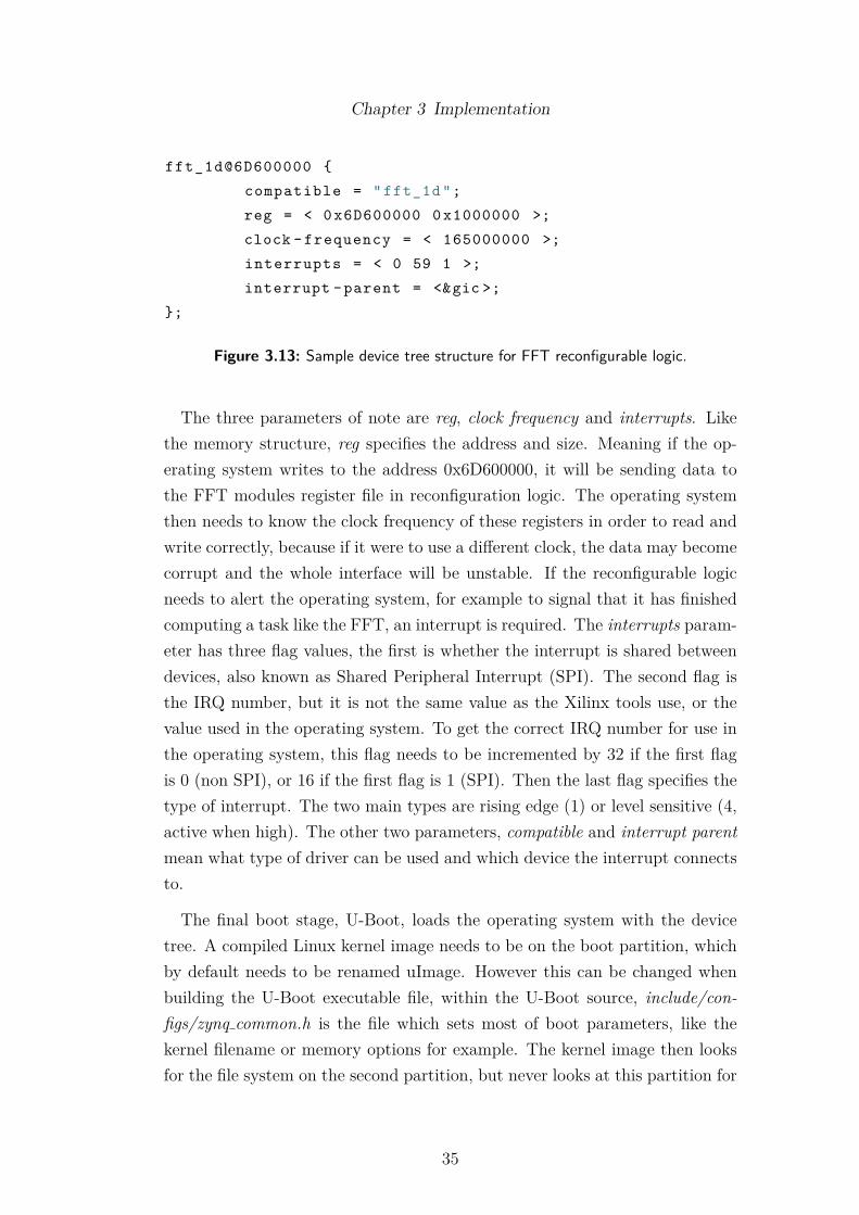
fft_1d@6D600000 {compatible = " fft_1d ";reg = < 0 x6D600000 0 x1000000 >;clock - frequency = < 165000000 >;interrupts = < 0 59 1 >;interrupt - parent = <&gic >;
};
Figure 3.13: Sample device tree structure for FFT reconfigurable logic.
The three parameters of note are reg, clock frequency and interrupts. Likethe memory structure, reg specifies the address and size. Meaning if the op-erating system writes to the address 0x6D600000, it will be sending data tothe FFT modules register file in reconfiguration logic. The operating systemthen needs to know the clock frequency of these registers in order to read andwrite correctly, because if it were to use a di�erent clock, the data may becomecorrupt and the whole interface will be unstable. If the reconfigurable logicneeds to alert the operating system, for example to signal that it has finishedcomputing a task like the FFT, an interrupt is required. The interrupts param-eter has three flag values, the first is whether the interrupt is shared betweendevices, also known as Shared Peripheral Interrupt (SPI). The second flag isthe IRQ number, but it is not the same value as the Xilinx tools use, or thevalue used in the operating system. To get the correct IRQ number for use inthe operating system, this flag needs to be incremented by 32 if the first flagis 0 (non SPI), or 16 if the first flag is 1 (SPI). Then the last flag specifies thetype of interrupt. The two main types are rising edge (1) or level sensitive (4,active when high). The other two parameters, compatible and interrupt parentmean what type of driver can be used and which device the interrupt connectsto.
The final boot stage, U-Boot, loads the operating system with the devicetree. A compiled Linux kernel image needs to be on the boot partition, whichby default needs to be renamed uImage. However this can be changed whenbuilding the U-Boot executable file, within the U-Boot source, include/con-figs/zynq common.h is the file which sets most of boot parameters, like thekernel filename or memory options for example. The kernel image then looksfor the file system on the second partition, but never looks at this partition for
35

Chapter 3 Implementation
another kernel. Therefore any changes to the kernel need to be compiled intoan image, and placed on the boot partition. Simpling rebuilding the kernelwhile it is running then rebooting the Zedboard will not load the new kernel.
3.4.2 Driver
The operating system treats the reconfigurable logic as any other device, whichmeans it requires a driver to communicate with it. A character driver, whichsends/receives byte by byte, was created for the FFT module to write thedata width, source address, and destination address to the registers within thereconfigurable logic, and also to handle the interrupt when the FFT compu-tation is complete. When writing a driver, or any other kernel module, it isimportant to remember that the code is not a separate program, it becomesa part of the kernel. Therefore all errors need to be handled appropriatelyto prevent system crashes, and also there are standards and templates thatshould be followed [37].
When the kernel sets up a driver for the device, the kernel needs to knowthe initialization and exit functions, like how programs need an entry point,often called the main function. But instead of standardising the functionnames, there are two built-in macros that are used to specify these func-tions, module init(driver init) and module exit(driver exit), where driver initand driver exit are functions within the driver.
Device drivers require a lot of information to operate, like the device name,address, and IRQ number. But these values change from system to system sothis information must be passed into the driver at runtime. This is achievedusing another built-in macro, module param(variable, type, permissions) asshown in Figure 3.14, which is a snippet of the implemented device driverand also shows how to provide a description of each parameter. How to passthese parameters to the driver is shown in the driver setup script in Figure 3.15.Where the insmod command installs the driver module into the running kernel,then mknod creates the character device driver node so it can actually beaccessed, and then the permissions are set.
The initialisation function is called when the driver is inserted into the run-ning kernel. It registers the device, and then requests and enables the inter-rupt. Because this is a character device, the register chrdev function was used,which takes the device major number, device name, and the file operations the
36

Chapter 3 Implementation
static long int register_address ;static long int register_length ;static char * device_name ;static int irq_number ;static int device_major ;
// Retrieve Parameters
module_param ( register_address , long , 0);MODULE_PARM_DESC ( register_address , "Base address for the
peripheral ");module_param ( register_length , long , 0);MODULE_PARM_DESC ( register_address , " Address length for
the peripheral ");module_param ( device_name , charp , 0);MODULE_PARM_DESC ( device_name , "Name of the peripheral ");module_param (irq_number , int , 0);MODULE_PARM_DESC (irq_number , "IRQ number for peripherals
interrupt ");module_param ( device_major , int , 0);MODULE_PARM_DESC ( device_major , " Major number of the
peripheral ");
Figure 3.14: Retrieving parameters in the device driver.
directory = /home/ linaro / fft_1d_drivermod_name = fft_1d .kobase = 0 x6D600000length = 0 x1000000name = " fft_1d "irq = 91mjor = 62dev_name = fft_1d_fpga
insmod / $directory / $mod_name register_address =$baseregister_length = $length device_name =$nameirq_number =$irq device_major =$mjor
mknod /dev/ $dev_name c $mjor 0chmod 700 /dev/ $dev_name
Figure 3.15: Device driver setup script.
driver supports. The operations supported by this driver get defined in thefile operations struct, shown in Figure 3.16. The read and llseek functions arenot actually required because data is only ever written from o�set 0, howeverthey were added for testing and possible future use. Enabling the interrupt
37
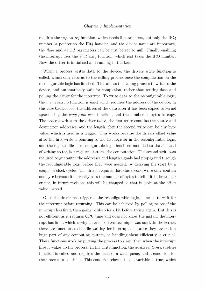
Chapter 3 Implementation
requires the request irq function, which needs 5 parameters, but only the IRQnumber, a pointer to the IRQ handler, and the device name are important,the flags and dev id parameters can be just be set to null. Finally enablingthe interrupt uses the enable irq function, which just takes the IRQ number.Now the driver is initialised and running in the kernel.
When a process writes data to the device, the drivers write function iscalled, which only returns to the calling process once the computation on thereconfigurable logic has finished. This allows the calling process to write to thedevice, and automatically wait for completion, rather than writing data andpolling the driver for the interrupt. To write data to the reconfigurable logic,the memcpy toio function is used which requires the address of the device, inthis case 0x6D60000, the address of the data after it has been copied to kernelspace using the copy from user function, and the number of bytes to copy.The process writes to the driver twice, the first write contains the source anddestination addresses, and the length, then the second write can be any bytevalue, which is used as a trigger. This works because the drivers o�set valueafter the first write is pointing to the last register in the reconfigurable logic,and the register file in reconfigurable logic has been modified so that insteadof writing to the last register, it starts the computation. The second write wasrequired to guarantee the addresses and length signals had propagated throughthe reconfigurable logic before they were needed, by delaying the start by acouple of clock cycles. The driver requires that this second write only containone byte because it currently uses the number of bytes to tell if it is the triggeror not, in future revisions this will be changed so that it looks at the o�setvalue instead.
Once the driver has triggered the reconfigurable logic, it needs to wait forthe interrupt before returning. This can be achieved by polling to see if theinterrupt has fired, then going to sleep for a bit before trying again. But this isnot e�cient as it requires CPU time and does not know the instant the inter-rupt has fired, which is why an event driven technique was used. In the kernel,there are functions to handle waiting for interrupts, because they are such ahuge part of any computing system, so handling them e�ciently is crucial.These functions work by putting the process to sleep, then when the interruptfires it wakes up the process. In the write function, the wait event interruptiblefunction is called and requires the head of a wait queue, and a condition forthe process to continue. This condition checks that a variable is true, which
38
Chapter 3 Implementation
struct file_operations driver_file_operations = {read: driver_read ,write: driver_write ,open: driver_open ,release : driver_release ,llseek : driver_llseek
};
Figure 3.16: File operations for the driver.
is set true by the interrupt handler, and set false at the start of the writefunction. So now the process is sleeping, and will only be woken when thewake up interruptible function is called by the interrupt handler. This func-tion also needs the address of the head of the wait queue, and will iterateover the queue, waking up every process. The woken processes then checktheir continue condition, if it is true they carry on executing, otherwise theygo back to sleep. In this driver, because only one process gets added to thequeue, it guarantees that when it gets woken up, that it is condition is true.Therefore only a few CPU instructions are used for sleeping, unlike the pollingmethod, improving the performance of the system. The write function for thedriver is shown in Appendix B.4 to highlight this event approach.
3.4.3 System Call
In order for a user space program to call the driver which handles the FFTmodule in the reconfigurable logic, a system call was added to the Linux kernel.It was implemented within the kernel rather than user-space, because insidethe kernel are a lot of useful functions with regards to memory management,which were required and it would allow for better handling of multiple userprograms trying to use the programmable logic at once. On x86 the processof adding a new system call is well documented, but for ARM there is verylittle, therefore grep was used to find the necessary source files by searchingfor known system calls. How these files were edited to add the �t 1d systemcall will now be described.
• arch/arm/kernel/calls.SThis file has a list of system calls, therefore add the custom call to theend. For this kernel version, the custom call has an o�set of 380.
39

Chapter 3 Implementation
/* 375 */ CALL( sys_setns )CALL( sys_process_vm_readv )CALL( sys_process_vm_writev )CALL( sys_kcmp )CALL( sys_finit_module )
/* 380 */ CALL( sys_fft_1d )
• arch/arm/include/asm/unistd.hBecause a new system call has been added, the number of calls needs tobe incremented by one.
# define __NR_syscalls (381)
• arch/arm/include/uapi/asm/unistd.hAdd the system call with its o�set.
# define __NR_setns ( __NR_SYSCALL_BASE +375)# define __NR_process_vm_readv ( __NR_SYSCALL_BASE +376)# define __NR_process_vm_writev ( __NR_SYSCALL_BASE +377)# define __NR_kcmp ( __NR_SYSCALL_BASE +378)# define __NR_finit_module ( __NR_SYSCALL_BASE +379)# define __NR_fft_1d ( __NR_SYSCALL_BASE +380)
• include/linux/syscalls.hAt the end of this file is where the system call is declared.
asmlinkage long sys_kcmp (pid_t pid1 , pid_t pid2 , inttype , unsigned long idx1 , unsigned long idx2);
asmlinkage long sys_finit_module (int fd , const char__user *uargs , int flags);
asmlinkage long sys_fft_1d (char *source , char *destin, int width);
# endif
• kernel/�t 1d.cCreate a source file for the new system call.
• kernel/MakefileEdit the kernel Makefile to include the �t 1d source.
obj -y = fork.o exec_domain .o panic.o printk .o \... \fft_1d .o
40

Chapter 3 Implementation
• arch/arm/kernel/entry-common.SThere was a small problem when compiling the kernel however, duringone check it was not picking up the updated system call properly, so inthis file a few lines were commented out to allow the kernel to compile.This has not caused any issues but it would need to be fixed in the future.
/*
.ifne NR_syscalls - __NR_syscalls
.error " __NR_syscalls is not equal to the size of the
syscall table"
.endif
*/
The primary purpose of the system call is to take the source and destinationmemory pointers, pass them to the driver and wait for the computation tocomplete before returning from the call. However because Linux uses virtualmemory addresses and the reconfigurable logic uses physical addresses, thetwo memory pointers been passed to the system call can not simply be passedstraight to the driver, they have to be converted into physical addresses first.Within the kernel there is a function virt to phys(virtual address) which willreturn the physical address, however the virtual address must be within thekernel address space, not user space meaning it will not work as expected forthe two pointer parameters. The next solution involved walking page tablesto manually find the physical address. This is well documented on the x86architecture but not very well on the ARM architecture, a recurring patternin this project.
The code in Appendix B.5 follows the idea described in Figure 3.17, thereare four tables which need to be walked before the physical address can bediscovered. The virtual address provides an o�set in the Page Global Directory(PGD) table, which gives a pointer to one Page Upper Directory (PUD) table.Then the virtual address is used again to provide an o�set in the PUD tableto find the pointer to the next table, Page Middle Directory (PMD). Thisprocess is the same for the PMD and Page Table Entry (PTE) tables thenthe pointer to the physical page is known. When this was implemented, theearly results seemed promising, the physical address did contain the test datathat was written to memory using the virtual address. However when a largearray of data was written to memory using virtual addresses, the physical
41

Chapter 3 Implementation
PGD PUD PMD PTE Page
Figure 3.17: Converting a virtual to physical address in Linux on ARM.
addresses often only contained parts of the array. Therefore the memory wasnot guaranteed to contain continuous data, which meant the reconfigurablelogic would read invalid data, because it starts reading from the given address,then increments the address until the whole array has been read. So walkingpage tables was not going to work for this projects needs. Since user space pagetables did not meet the requirements, the next method was to use kernel spacememory. It was possible to allocate continuous memory from within the kernel,however there were a few issues with this approach, memory alignment wasnot guaranteed automatically, and there was limited space within the kernelsmemory space meaning continuous memory was hard to come by, and it wouldeither mean giving the user program access to the kernels memory or copyingthe data from user space. All of these trade o�s meant another solution wasrequired.
In both user and kernel space, it is possible to map into physical memorydirectly for reading and writing data. The only problem being physical memoryis controlled by the kernel and it automatically swaps pages in and out, sothere is the danger of reading the wrong data because it has been overwrittenor writing over another processes memory. To get around these dangers, a bootparameter which tells the kernel its entry point into memory has been changedwhich allows some memory to be “hidden” from the kernel. This is possiblebecause the kernel enters at the highest address, and uses all the memorybelow that, so for the Zedboard changing the high address parameter from0x20000000 (512MB) to 0x19C00000 (412MB), allowed for 100MB of memorythat is safe to use directly.
This solution gives two options for implementation, performance and sim-plicity. The best performance is achieved by the user space program mapping
42
Chapter 3 Implementation
into physical memory, meaning the system call only needs to pass the physicaladdresses to the driver. This requires the code to be rewritten so it uses phys-ical memory directly, plus the program needs to handle addresses correctlyto avoid multiple processes or threads using the same address. However forsimplicity, the user space program can use virtual memory as usual, meaningwhen the system call is called, it has to figure out that it is a virtual address,and copy the memory from user space, to the free physical memory beforecalling the driver. Then when the driver returns, copy the memory back intouser space. This allows the program code to just use the system call, no otherchanges are needed within the code. It is also safer because the system callcan dynamically choose the physical address since it is aware of what is inuse. But this simplicity involves extra copying of data when compared to theperformance option, so there is a trade o� between the time to rewrite thecode and computation time.
3.4.4 Datapath
Traditional datapaths in reconfigurable logic are built to allow the design toexecute in parallel and are pipelined to increase throughput, however becausethis design involves software and hardware working together, a traditionaldatapath/pipeline design can not be applied. Instead the main datapath hasto be designed in software, with the hardware supporting a few functions likethe 1D FFT that can be executed in parallel, however recalling the floor planof the FFT design in Appendix B.3, available space is an issue which limits theamount of FFT modules that can be implemented, so the software datapathhas to be designed to share the FFT hardware modules.
Within software, in order to get functions working in parallel, threads arerequired, which initially sounds like a dreadful idea when dealing with a mem-ory bandwidth bottleneck, however because most of the intensive computationis now in reconfiguration logic, this does not become an issue. So to pipelinethe algorithm in software to guarantee 30 FPS, functions have to be created sothat their executed time is under 1/30th of a second, with each thread runningthe sequence of functions at di�erent phases with each other, then when thenext frame is ready, they start executing the next function in their sequence,creating a pipeline for the frame to flow through, resulting in the output being30 FPS. Because the algorithm requires five 2D FFTs, the functions have toequally share the available FFT modules so that no thread will be starved,
43

Chapter 3 Implementation
which would break the pipeline. This type of design results in the softwareacting like a controller for the hardware, while also computing the smallerfunctions, and shows the true potential of coupling a FPGA and an ARMCortex-A9 on the same chip.
44

4
Results and Discussion
“I came here to drink milk and kick ass. AndI’ve just finished my milk.”
— Maurice Moss, The IT Crowd
This chapter presents the results for the x86 architecture, ARM architecture,and the Fast Fourier Transform (FFT) module in reconfigurable logic, thenwill discuss the findings in the discussion section. All timing benchmarks showcomputation time only, with read/write delays from the storage device factoredout.
4.1 Results
4.1.1 Intel x86 Performance
The x86 benchmarks were performed using an early 2013 MacBook Pro Retina13”, which is equipped with a 2.6GHz Intel Core i5-3230M, 8GB 1600MHzDDR3, and a 128GB solid state drive.
Three di�erent versions of the code were benchmarked: an initial imple-mentation in C as a baseline the refactored version which has improved cachelocality and common computation factored, and the last version which usesAVX. The results are shown in Figure 4.1 using an array size of 2048x2048,and note that all three stages use the optimized FFTS library, so the FFTcomputation time is consistent, with the rest of algorithm being improved.
45

Chapter 4 Results and Discussion
Baseline Refactor Intrinsics0
0.5
1
1.5
2
2.5
3
Implementation
Seco
nds
Per
Fram
e
Figure 4.1: Intel x86 Performance with an array size of 2048x2048.
The results show the importance of having knowledge of the CPU’s cacheand only computing common values once, as it nearly halved the computationtime per frame over the baseline version. They also show the raw performanceavailable with vector intrinsics, which nearly decreases computation time by athird over the refactored version, and this time could be further improved byusing the latest Intel Haswell chips which support AVX2.
When working with a 720p image stream (1280x720), using an array size of2048x2048 for computing the 2D FFTs requires a lot of zero padding as shownin Figure 4.2a, where the blue rectangle represents the image, and the grayis padding. This results in the array containing nearly 80% padding, and theremaining 20% being the actual data. This is a lot of wasted computationtime, so instead of padding up to the next power of two, reduce the arraysize to the previous power of two, meaning an array of 2048x2048 becomes1024x1024. For a 720p image, this only results in slicing 10% o� each sideas shown in Figure 4.2b, however there is still enough image data for this notto impact the quality of the output results, assuming the sliced 20% does notcontain the only useful data in the whole image.
Figure 4.3 shows how reducing the array size impacts the computation timerequired per frame. These arrays sizes can be applied to any image resolu-tion, however using either a 256x256 or 512x512 array size for a 720p image
46

Chapter 4 Results and Discussion
(a) 2048x2048 (b) 1024x1024
Figure 4.2: 720p image using an array size of 2048x2048 and 1024x1024.
256 512 1024 20480
0.1
0.2
0.3
0.4
0.5
30 FPS
2D Array Size
Seco
nds
Per
Fram
e
Figure 4.3: Intel x86 Performance for the working array size.
will produce poor quality results, however for smaller image resolutions, thisalgorithm is close to running in real-time at 30 Frames Per Second (FPS).By reducing the array size from 2048x2048 to 1024x1024 for the 720p image,improves the computation time per frame by a factor of three, giving over7 FPS. Google claim 10 FPS [20][19] for their image stabilisation algorithmon a single machine, so even though this algorithm is running on a MacBook,and uses the very computationally intense 2D FFT function five times, the
47
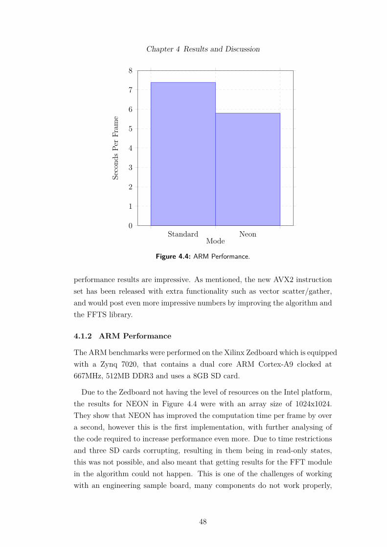
Chapter 4 Results and Discussion
Standard Neon0
1
2
3
4
5
6
7
8
Mode
Seco
nds
Per
Fram
e
Figure 4.4: ARM Performance.
performance results are impressive. As mentioned, the new AVX2 instructionset has been released with extra functionality such as vector scatter/gather,and would post even more impressive numbers by improving the algorithm andthe FFTS library.
4.1.2 ARM Performance
The ARM benchmarks were performed on the Xilinx Zedboard which is equippedwith a Zynq 7020, that contains a dual core ARM Cortex-A9 clocked at667MHz, 512MB DDR3 and uses a 8GB SD card.
Due to the Zedboard not having the level of resources on the Intel platform,the results for NEON in Figure 4.4 were with an array size of 1024x1024.They show that NEON has improved the computation time per frame by overa second, however this is the first implementation, with further analysing ofthe code required to increase performance even more. Due to time restrictionsand three SD cards corrupting, resulting in them being in read-only states,this was not possible, and also meant that getting results for the FFT modulein the algorithm could not happen. This is one of the challenges of workingwith an engineering sample board, many components do not work properly,
48

Chapter 4 Results and Discussion
FFTS Simple Advanced0
500
1,000
1,500
2,000
2,500
3,000
System CallsFFT Function
Mic
rose
cond
s
Figure 4.5: Software vs. Hardware: FFT computation of an array size 2048.
and given that three SD cards have become corrupted, the board is probablyat fault. There have been a few known issues regarding the SD card reader [4],but these do not mention corruption.
4.1.3 FPGA Performance
The Field-Programmable Gate Array (FPGA) benchmarks were performed onthe Xilinx Zedboard which is equipped with a Zynq 7020 packaging a dualcore ARM Cortex-A9 clocked at 667MHz and an Artix 7 FPGA. The boardalso has 512MB DDR3 and uses a 8GB SD card.
Figure 4.5 compares computing the 1D FFT of a transform size of 2048on the Xilinx Zedboard using the FFTS library on the ARM, and the FFTmodule in the reconfigurable logic developed in this project. The FFT moduleresults are in two sets: the first, labeled simple system call, where the userprogram calls the system call with virtual pointers and requires the kernelto copy the virtual memory to the known physical memory location. Thenthe second, labeled advanced system call, is where the kernel only needs topass the physical addresses to the driver, and no copying is required because
49
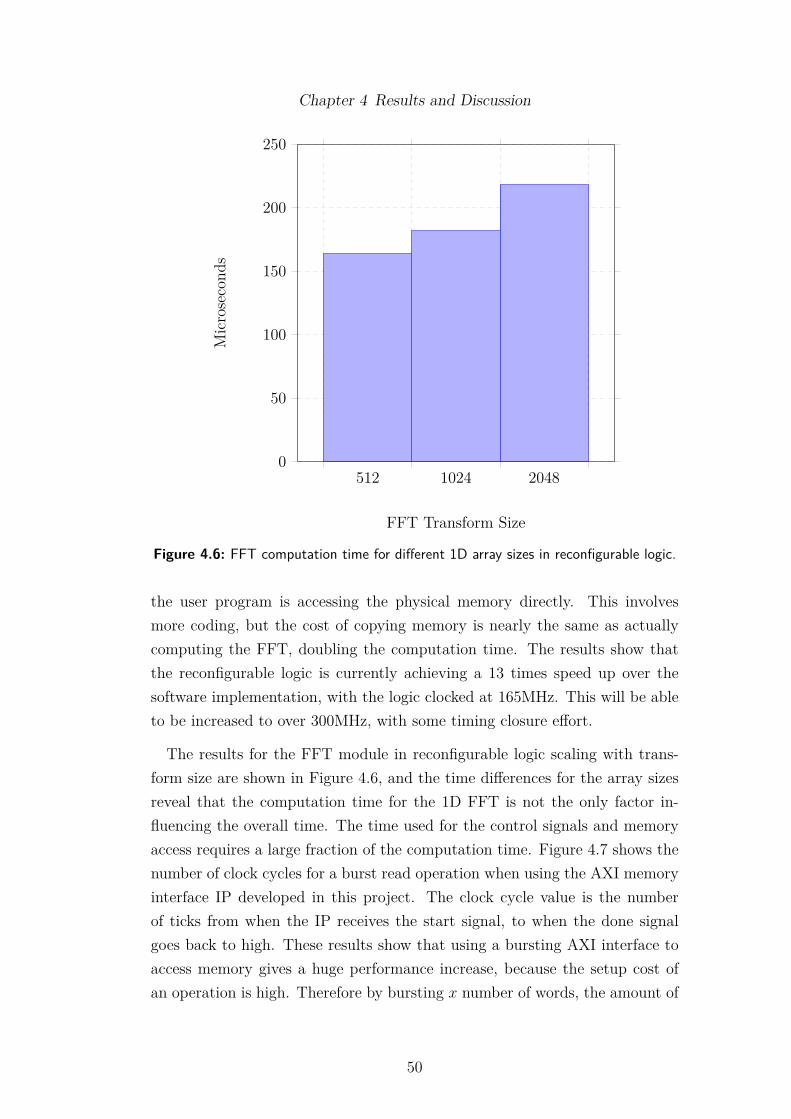
Chapter 4 Results and Discussion
512 1024 20480
50
100
150
200
250
FFT Transform Size
Mic
rose
cond
s
Figure 4.6: FFT computation time for di�erent 1D array sizes in reconfigurable logic.
the user program is accessing the physical memory directly. This involvesmore coding, but the cost of copying memory is nearly the same as actuallycomputing the FFT, doubling the computation time. The results show thatthe reconfigurable logic is currently achieving a 13 times speed up over thesoftware implementation, with the logic clocked at 165MHz. This will be ableto be increased to over 300MHz, with some timing closure e�ort.
The results for the FFT module in reconfigurable logic scaling with trans-form size are shown in Figure 4.6, and the time di�erences for the array sizesreveal that the computation time for the 1D FFT is not the only factor in-fluencing the overall time. The time used for the control signals and memoryaccess requires a large fraction of the computation time. Figure 4.7 shows thenumber of clock cycles for a burst read operation when using the AXI memoryinterface IP developed in this project. The clock cycle value is the numberof ticks from when the IP receives the start signal, to when the done signalgoes back to high. These results show that using a bursting AXI interface toaccess memory gives a huge performance increase, because the setup cost ofan operation is high. Therefore by bursting x number of words, the amount of
50
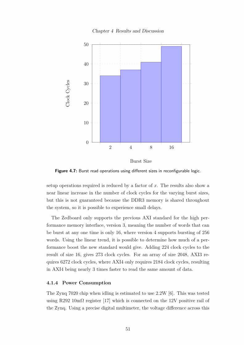
Chapter 4 Results and Discussion
2 4 8 160
10
20
30
40
50
Burst Size
Clo
ckC
ycle
s
Figure 4.7: Burst read operations using di�erent sizes in reconfigurable logic.
setup operations required is reduced by a factor of x. The results also show anear linear increase in the number of clock cycles for the varying burst sizes,but this is not guaranteed because the DDR3 memory is shared throughoutthe system, so it is possible to experience small delays.
The Zedboard only supports the previous AXI standard for the high per-formance memory interface, version 3, meaning the number of words that canbe burst at any one time is only 16, where version 4 supports bursting of 256words. Using the linear trend, it is possible to determine how much of a per-formance boost the new standard would give. Adding 224 clock cycles to theresult of size 16, gives 273 clock cycles. For an array of size 2048, AXI3 re-quires 6272 clock cycles, where AXI4 only requires 2184 clock cycles, resultingin AXI4 being nearly 3 times faster to read the same amount of data.
4.1.4 Power Consumption
The Zynq 7020 chip when idling is estimated to use 2.2W [6]. This was testedusing R292 10m� register [17] which is connected on the 12V positive rail ofthe Zynq. Using a precise digital multimeter, the voltage di�erence across this
51

Chapter 4 Results and Discussion
Zynq Zynq-FPGA i50
10
20
30
CPU
Wat
ts
Figure 4.8: Power Usage.
register when the board is in a default state was 1.83mV. Using the equationV/R = I, 0.00183/0.010 gives a current value of 0.183A. Then to find thepower usage, P = V I, 12 ◊ 0.183 which results in 2.196W.
Vivado gives an estimate of the power consumption for the design in recon-figurable logic, 1.8W, but there are many factors influencing this value and it isnot very accurate. However using the R292 register, the overall power that theZynq chip requires can be calculated using the physical circuitry when the FFTmodule is running. The multimeter gave a 3.16mV voltage di�erence acrossthe register, which gives a current value of 0.318A (0.00316/0.010), resulting inthe power usage being 3.792W (12◊0.318). Therefore the total power usage ofthis design when idling is 3.792W, with the power usage of the reconfigurablelogic at 1.596W. The multimeter reported the same readings when the FFTwas being computed in the reconfigurable logic, which probably means thesampling rate of the multimeter was not fast enough, so it would be safe toassume the power usage would increase slightly during the computation time,but for the meter not to pick this up, it is only increasing for a very shortperiod of time.
It is di�cult to know how much power the Intel i5-3230M CPU is drawing,however the CPU alone is rated at 35W Thermal Design Power (TDP) [24],with other components using a lot of power also, for example the memory.Therefore the MacBook will be drawing a great deal more power than that of
52
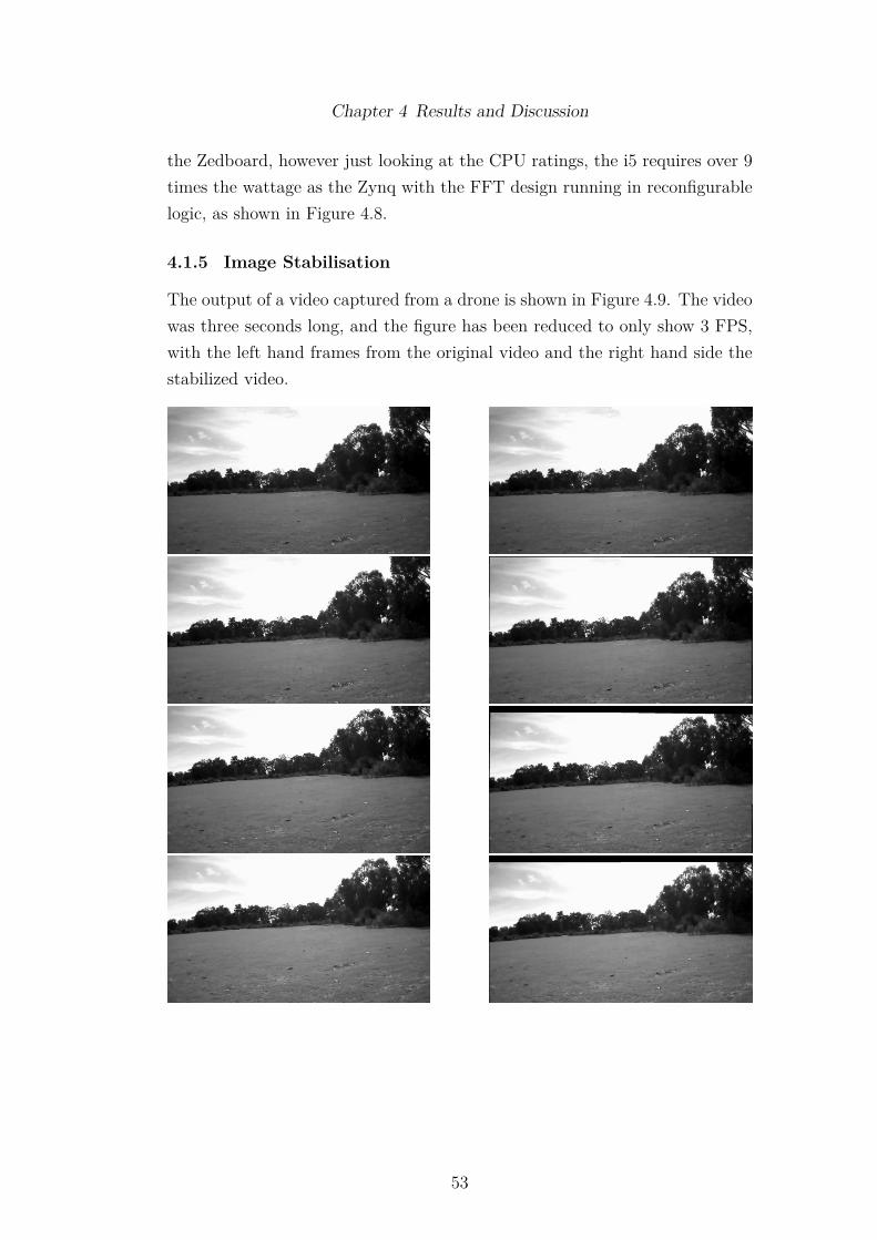
Chapter 4 Results and Discussion
the Zedboard, however just looking at the CPU ratings, the i5 requires over 9times the wattage as the Zynq with the FFT design running in reconfigurablelogic, as shown in Figure 4.8.
4.1.5 Image Stabilisation
The output of a video captured from a drone is shown in Figure 4.9. The videowas three seconds long, and the figure has been reduced to only show 3 FPS,with the left hand frames from the original video and the right hand side thestabilized video.
53

Chapter 4 Results and Discussion
Figure 4.9: Three second video from drone, showing 3 FPS. Left is the input and rightis the output.
54
Chapter 4 Results and Discussion
4.2 Discussion
4.2.1 Image Stabilisation
In Figure 4.9, looking at the input sequence first, focusing on where the grasstouches the sides and the orientation of the grass, it is easy to see the videogoing up and down with roll from the drone cause by wind. Compared tothe output video, the grass touches the sides at roughly the same height androtation stays constant. The amount of correction is easy to see because ofthe black around the frame caused by moving and rotation the frame. Theseresults are very positive and show that the rotation has been minimised. Thetranslation is also being correctly removed for this video with the algorithmtreating the drone as a fixed camera, like a security camera mounted on a polein the wind. However more work needs to be done to handle the drone flyingaround, currently a basic solution is in place where it looks at the previous Nframes to average the translation, but a more advanced technique is required.
4.2.2 David vs. Goliath
The results from the Intel i5 processor showcase its raw performance, andwith the next generation of AVX released, Goliath has become even stronger,appearing to crush the little ARM chip. However David brought a secretweapon to the fight, an FPGA. Looking at the NEON results, they appearto be far worse than that of Intel, however they do not tell the whole story.Given the troubles experienced with the SD cards, the code could not befurther developed, nor could the FFT in reconfigurable logic be used within thealgorithm. The computation time for NEON code of a array of size 1024x1024should be able to be decreased by over a second. When the reconfigurable logicis used, which currently gives a 13 times speed up for the 1D FFT, and becausethe FFT makes up over half of computation, the time will be decreased by atleast a factor of 7, resulting in around 0.7 seconds per frame. Now taking intoconsideration the power requirements of both systems, the i5 alone draws 9times the amount of power required by the Zynq, but only gives 5 times theperformance, plus the other components in the MacBook are using far morepower than the Zedboard. Therefore in terms of throughput per power, theZynq platform demolishes the Intel platform.
55
Chapter 4 Results and Discussion
4.2.3 Developer Time
During this project, there was approximately an equal amount of time spentdeveloping the software and hardware, with both requiring new concepts whichmeant the overall development time took longer due to the steep learning curve.Learning how the initial algorithm worked with regards to the FFT and othertransforms, to analysis and improve upon it, was more time consuming thanlearning how to use AVX and NEON because FFTs are not an easy transformto master. The hardware development was the opposite, with most of thetime spent debugging and testing on the Zedboard to get components workingcorrectly. To put it in context, over a month of late nights was spent getting theDDR3 AXI interface working reliably on the Zedboard, then actually buildingthe controller IP component for use in the project. This time was mostly dueto the lack of documentation and examples available for using the interface.A lot of this learning and testing time is a one o� cost, and can be appliedto other projects, so developing parts of an algorithms to run reconfigurablelogic does not add a significant amount of development time, given the hugeperformance gain that it gives.
Vivado when compared to the previous design suite was fair easier to use, andas a whole felt faster to development because there was not the need to keepswitching tools. The 2013 version of Vivado supported the Xilinx Zedboardwhich meant there was not configuration mismatch issues experienced withthe older suite, however the biggest improvement was the debugging, the timeto setup and probe a debug core has reduced significantly, which in termsof this project, saved days of debugging. Another tool was used to speedup the development process of the HDL, Aquamacs VHDL mode [2]. IdeallyVivado would have this editor built-in for writing HDL, because there currentimplementation is basically just a text editor, unlike Aquamacs which canautomatically generate a lot of code.
56
5
Conclusion
5.1 Revisiting the Hypotheses
After testing the hypothesis outlined in Chapter 1, the results presented inChapter 5 show the performance gains of e�ciently using the underlying hard-ware, o�ering over 80% faster performance over a naive implementation, with-out a�ecting the output quality of the algorithm. In terms of power usage, theresults in this thesis show that adding custom hardware does increase powerusage by approximately 70%, however gives 13 times the performance whichis a positive trade o�. Developer time is discussed in Section 4.2.3 of this the-sis, and details that once the steep learning curve is overcome, the additionaldevelopment time to add custom hardware on the Zedboard is minimum whencompared to the performance gains, and it also details that writing the algo-rithm so that it uses the micro-processor e�ciently, involves very little extradevelopment time as well.
5.2 Contributions and Future Work
5.2.1 Image Stabilisation
The current implementation performs very well, however it could be improvedby also handling ego motion. Treating the camera as a fixed node was adequatefor this project, however being able to stabilise video from a car or drone wouldgive this algorithm more applications. There are already techniques [20][27]that look into handling movement and these could be implemented. Also the
57
Chapter 5 Conclusion
quality of the output frames could be improved by trying to fill in the blackspace created by the correction, and then other warps to remove issues likethe distortion caused by rolling shutters [33][19]. Even though a new imagestabilisation algorithm has been developed in this project, which has beenoptimised to use five 2D FFTs, less than other solutions researched [50][32],all of these improvements were out of the scope of this project. Because thegoal was to evaluate performance optimisations and the FFT, not to try andget the best output quality possible, which is a vast project all in itself.
5.2.2 Software Optimisations
Results from this project show how di�cult it is to get computationally intenseimage processing algorithms running in real-time with large resolutions. How-ever with Intel releasing the Haswell generation which supports scatter/gather,or the use of higher end hardware, the algorithm could manage real-time per-formance, so this is an area which can be explored in the future. The NEONintrinsics also need to be further optimised and improved upon, which due tofaults in the engineering sample of the Zedboard, could not be accomplishedin this projects time period. The software optimisations that were completedduring this project really show the importance of having knowledge of theunderlying architecture is when performance is a concern.
5.2.3 Hardware
The FFT module in the reconfigurable logic is currently out performing thesoftware FFT by a factor of 13. However these results can still be improvedas the FFT core is only running at 165MHz, but also this implementation isnot fully taking advantage of the full potential of the FPGA, as it is not veryparallel. The FFT core supports many channels, allowing multiple FFTs to becomputed at once, while also allowing the transpose for the 2D FFT to occurin reconfigurable logic. Plus the reconfigurable logic has a total of four memorychannels available, with one only currently used, therefore fully optimising thememory and FFT core channels, will increase the performance of the FFTmodule by well over a factor of 4. In total, there is room for another order ofmagnitude of improvement.
A motion estimation project [35][36] by John Perrone, will be using the FFTmodule in reconfigurable logic, the Linux driver, and the system call developedin this project, combined with the knowledge gained of the Zynq 7020 chip, to
58
Chapter 5 Conclusion
improve the computation time of the estimation algorithm in order to achievereal-time performance, while also lowering the power requirements. The endgoal will be designing and building an autonomous drone controller whichwill be on board a quadro copter, hence why power usage is so important.There will also be the need for other computationally intense functions to beimplemented in the reconfigurable logic as well. With the lack of documenta-tion available for the Zedboard, this project will be able to help many otherprojects, especially with regards to communicating with the DDR3 memoryinterface, and the possible release of the DDR3 interface IP component to theZedboard community. Consequently this project has a real-world applicationand will have some lasting impact.
5.3 Final Remarks
This thesis showed that using the underlying hardware e�ciently can drasti-cally improve the performance of computationally intense algorithms, and itis possible to further accelerate these algorithms by using custom hardwarewithout a huge increase in the power usage. They also show that a low powerZynq chip beats an Intel i5 in terms of throughput per power, which is veryimpressive.
59

Chapter 5 Conclusion
FIN.
60

References
[1] Linaro. http://www.linaro.org/linux-on-arm (Accessed October 2013).
[2] Vhdl mode. http://www.iis.ee.ethz.ch/ zimmi/emacs/vhdl-mode.html(Accessed October 2013).
[3] Helder Araujo and Jorge M. Dias. An Introduction to the Log-Polar Map-ping. Department of Electrical Eng. University of Coimbra, 1997.
[4] Avnet, Inc. ZedBoard Rev C.1 Errata, 1.3 edition, May 2013.
[5] Sebastiano Battiato, Giovanni Gallo, Giovanni Puglisi, and Salvatore Scel-lato. Sift features tracking for video stabilization. pages 825–830, 2007.
[6] Jim Beneke. Zynq™-7000 EPP in Action: Exploring ZedBoard. Avnet,2012.
[7] Anthony M Blake. Dynamically generating �t code on mobile devices.
[8] Anthony M Blake. Computing the fast Fourier transform on SIMD mi-croprocessors. PhD thesis, University of Waikato, 2012.
[9] Anthony M Blake, Ian H Witten, and Michael J Cree. The fastest fouriertransform in the south. 2013.
[10] E Oran Brigham. The Fast Fourier Transform and its applications. Pren-tice Hall, 1988.
[11] Rita Cucchiara, Costantino Grana, Massimo Piccardi, and Andrea Prati.Detecting moving objects, ghosts, and shadows in video streams. PatternAnalysis and Machine Intelligence, IEEE Transactions on, 25(10):1337–1342, 2003.
[12] Andrew J Davison. Real-time simultaneous localisation and mapping witha single camera. pages 1403–1410, 2003.
61
References
[13] Dmitri Dolgov, Sebastian Thrun, Michael Montemerlo, and James Diebel.Path planning for autonomous vehicles in unknown semi-structured envi-ronments. The International Journal of Robotics Research, 29(5):485–501,2010.
[14] Doulos. The Verilog® Golden Reference Guide, 1996.
[15] Alexandre Francois and Gerard Medioni. A modular software architecturefor real-time video processing. Computer Vision Systems, pages 35–49,2001.
[16] Matteo Frigo. A Fast Fourier Transform Compiler. MIT Laboratory forComputer Science, February 1999.
[17] GMAD. ZedBoard Schematic. Digilent, c.1 edition, June 2012.
[18] Chris Gregg and Kim Hazelwood. Where is the data? why you cannot de-bate cpu vs. gpu performance without the answer. Performance Analysisof Systems and Software (ISPASS), 2011 IEEE International Symposiumon, pages 134–144, 2011.
[19] Matthias Grundmann, Vivek Kwatra, Daniel Castro, and Irfan Essa.Calibration-free rolling shutter removal. 2012.
[20] Matthias Grundmann, Vivek Kwatra, and Irfan Essa. Auto-directed videostabilization with robust l1 optimal camera paths. 2011.
[21] HARDI Electronics AB. VHDL Handbook, 2000.
[22] Scott Hauck and Andre DeHon. Reconfigurable computing: the theory andpractice of FPGA-based computation. Morgan Kaufmann, 2010.
[23] National Instruments. Chapter 5: Customizing hardware through lab-view fpga. http://www.ni.com/pdf/products/us/criodevguidesec3.pdf(Accessed October 2013).
[24] Intel. Mobile 3rd Generation Intel® Core™ Processor Family, MobileIntel® Pentium® Processor Family, and Mobile Intel® Celeron® ProcessorFamily, datasheet, volume 1 of 2 edition, June 2013.
[25] Bruce Jacob, Spencer Ng, and David Wang. Memory systems: cache,DRAM, disk. Morgan Kaufmann, 2010.
[26] Vitit Kantabutra. On hardware for computing exponential and trigono-
62

References
metric functions. IEEE Transactions on Computers, 45(3):328–339, 1996.
[27] Alexandre Karpenko, David Jacobs, Jongmin Baek, and Marc Levoy. Dig-ital video stabilization and rolling shutter correction using gyroscopes.2011.
[28] Patent: Jean Laroche. Multi-microphone active noise cancellation system.
[29] Victor W Lee, Changkyu Kim, Jatin Chhugani, Michael Deisher, DaehyunKim, Anthony D Nguyen, Nadathur Satish, Mikhail Smelyanskiy, SrinivasChennupaty, Per Hammarlund, et al. Debunking the 100x gpu vs. cpumyth: an evaluation of throughput computing on cpu and gpu. ACMSIGARCH Computer Architecture News, 38(3):3451–460, 2010.
[30] Paralant Ltd. Ffts on the multi-core anemone processor. 2012.
[31] John Marko�. Google cars drive themselves, in tra�c. The New YorkTimes, 10:A1, 2010.
[32] JR Martinez-de Dios and Anıbal Ollero. A real-time image stabilizationsystem based on fourier-mellin transform. pages 376–383, 2004.
[33] Marci Meingast, Christopher Geyer, and Shankar Sastry. Geometric mod-els of rolling-shutter cameras. arXiv preprint cs/0503076, 2005.
[34] Hong Shan Neoh and Asher Hazanchuk. Adaptive edge detection for real-time video processing using fpgas. 2004.
[35] John A Perrone and Leland S Stone. A model of self-motion estimationwithin primate extrastriate visual cortex. Vision research, 34(21):2917–2938, 1994.
[36] John A Perrone, Alexander Thiele, et al. Speed skills: measuring thevisual speed analyzing properties of primate mt neurons. Nature neuro-science, 4(5):526–532, 2001.
[37] Michael Burian Peter Jay Salzman and Ori Pomerantz. The Linux KernelModule Programming Guide, 2.6.4 edition, 2007.
[38] Dapeng Oliver Wu Qin Chen. Realtime H.264 Encoding and DecodingUsing FFmpeg and x264. Dept. of Electrical & Computer Engineering,University of Florida, Gainesville, FL 32611, USA.
[39] B Srinivasa Reddy and BN Chatterji. An �t-based technique for transla-
63

References
tion, rotation, and scale-invariant image registration. Image Processing,IEEE Transactions on, 5(8):1266–1271, 1996.
[40] Cynthia Rodriguez. Understanding FFT-based algorithm to calculate im-age displacements with IDL programming language. University of Texasat San Antonio, 2007.
[41] Andrzej Ruta, Yongmin Li, and Xiaohui Liu. Real-time tra�c sign recog-nition from video by class-specific discriminative features. Pattern Recog-nition, 43(1):416–430, 2010.
[42] Daniel Scharstein and Amy J Briggs. Real-time recognition of self-similarlandmarks. Image and Vision Computing, 19(11):763–772, 2001.
[43] Sanjay Singh, Anil Kumar Saini, and Ravi Saini. Real-time fpga basedimplementation of color image edge detection. International Journal ofImage, Graphics and Signal Processing (IJIGSP), 4(12):19, 2012.
[44] Vasily Volkov. Better performance at lower occupancy. In Proceedings ofthe GPU Technology Conference, GTC, volume 10.
[45] Patent: Kaenel Vincent R. Von. Flexible packaging for chip-on-chip andpackage-on-package technologies.
[46] Liang Wang, Minglun Gong, Chenxi Zhang, Ruigang Yang, Cha Zhang,and Yee-Hong Yang. Automatic real-time video matting using time-of-flight camera and multichannel poisson equations. International journalof computer vision, 97(1):104–121, 2012.
[47] Holger Winnemoller, Sven C Olsen, and Bruce Gooch. Real-time videoabstraction. 25(3):1221–1226, 2006.
[48] Charles Wu. Implementing the Radix-4 Decimation in Frequency (DIF)Fast Fourier Transform (FFT) Algorithm Using a TMS320C80 DSP.Texas Instruments, January 1998.
[49] Stephan Wurmlin, Edouard Lamboray, and Markus Gross. 3d video frag-ments: Dynamic point samples for real-time free-viewpoint video. Com-puters & Graphics, 28(1):3–14, 2004.
[50] Hongjie Xie, Nigel Hicks, G Randy Keller, Haitao Huang, and VladikKreinovich. An idl/envi implementation of the �t-based algorithm for au-tomatic image registration. Computers & Geosciences, 29(8):1045–1055,
64
References
2003.
[51] Xilinx. 7 Series FPGAs Clocking Resources, v1.8 edition, August 2013.
[52] Xilinx. LogiCORE IP Fast Fourier Transform v9.0, Product Guide forVivado Design Suite, March 2013.
[53] Xilinx. Zynq-7000 All Programmable SoC Overview, v1.5 edition, Septem-ber 2013.
[54] Changsheng Xu, Kong Wan, Son Bui, and Qi Tian. Implanting virtualadvertisement into broadcast soccer video. Advances in Multimedia In-formation Processing-PCM 2004, 2005.
65

A
Image Stabilisation
66

Appendix A Image Stabilisation
A.1 C code for computing the 1D FFT1 void fft_execute_1d ( float *vector , int N, int sign) {2 int mmax , index_step , i, j ,m;3 float theta , temp , wpr , wpi , wr , wi , tr , ti;4
5 fft_rearrangeVector ( vector );6
7 mmax = 2;8 while (mmax < N) {9 index_step = mmax * 2;
10 theta = sign * (2 * PI / mmax);11 temp = sinf (0.5 * theta );12 wpr = -2.0f * temp * temp;13 wpi = sinf( theta );14 wr = 1.0f;15 wi = 0.0f;16 for(m = 1; m < mmax; m += 2) {17 for(i = m; i <= N; i+= index_step ) {18 j = i + mmax;19 tr = wr * vector [j - 1] - wi * vector [j];20 ti = wr * vector [j] + wi * vector [j - 1];21 vector [j - 1] = vector [i - 1] - tr;22 vector [j] = vector [i] - ti;23 vector [i - 1] += tr;24 vector [i] += ti;25 }26 wr = (temp = wr) * wpr - wi * wpi + wr;27 wi = wi * wpr + temp * wpi + wi;28 }29 mmax = index_step ;30 }31 }
67
B
Implementation
68
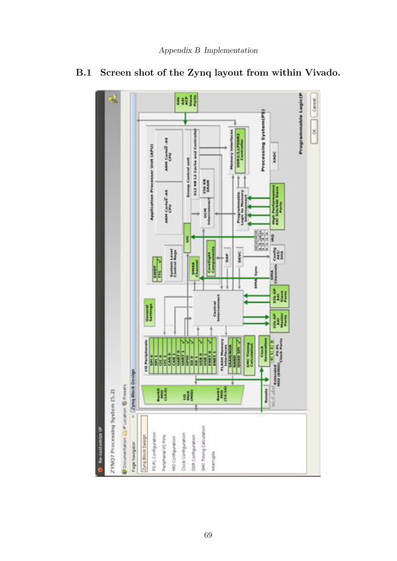
Appendix B Implementation
B.1 Screen shot of the Zynq layout from within Vivado.
69
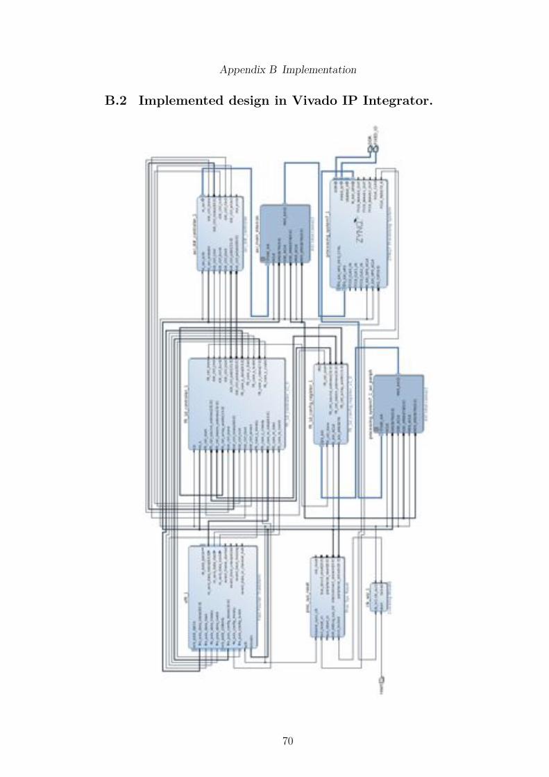
Appendix B Implementation
B.2 Implemented design in Vivado IP Integrator.
70
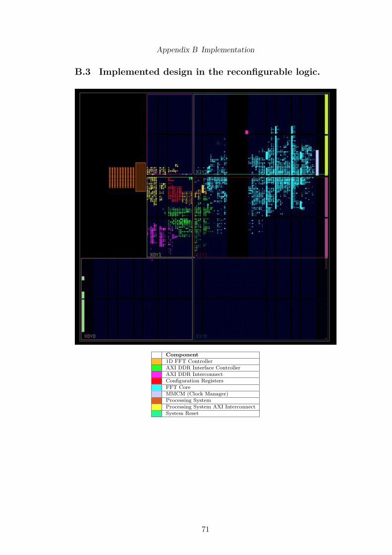
Appendix B Implementation
B.3 Implemented design in the reconfigurable logic.
Component
1D FFT Controller
AXI DDR Interface Controller
AXI DDR Interconnect
Configuration Registers
FFT Core
MMCM (Clock Manager)
Processing System
Processing System AXI Interconnect
System Reset
71
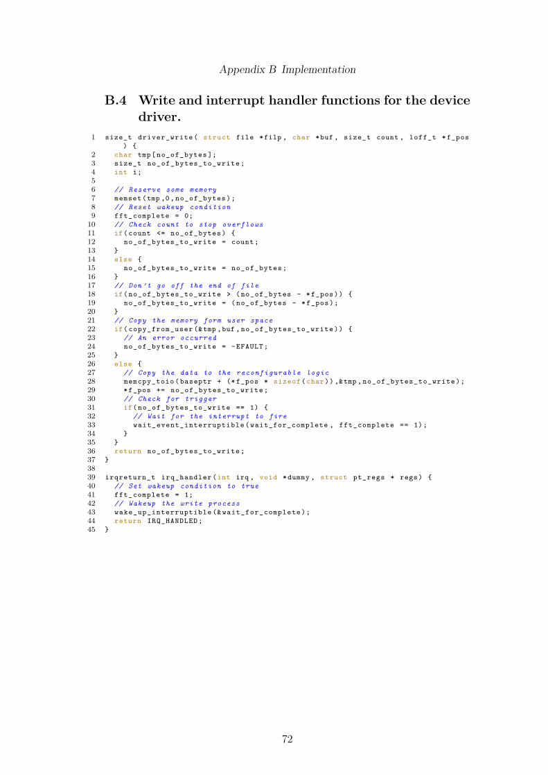
Appendix B Implementation
B.4 Write and interrupt handler functions for the devicedriver.
1 size_t driver_write ( struct file *filp , char *buf , size_t count , loff_t * f_pos) {
2 char tmp[ no_of_bytes ];3 size_t no_of_bytes_to_write ;4 int i;5
6 // Reserve some memory
7 memset (tmp ,0, no_of_bytes );8 // Reset wakeup condition
9 fft_complete = 0;10 // Check count to stop overflows
11 if( count <= no_of_bytes ) {12 no_of_bytes_to_write = count ;13 }14 else {15 no_of_bytes_to_write = no_of_bytes ;16 }17 // Don ’t go off the end of file
18 if( no_of_bytes_to_write > ( no_of_bytes - * f_pos )) {19 no_of_bytes_to_write = ( no_of_bytes - * f_pos );20 }21 // Copy the memory form user space
22 if( copy_from_user (&tmp ,buf , no_of_bytes_to_write )) {23 // An error occurred
24 no_of_bytes_to_write = -EFAULT ;25 }26 else {27 // Copy the data to the reconfigurable logic
28 memcpy_toio ( baseptr + (* f_pos * sizeof (char)) ,&tmp , no_of_bytes_to_write );29 * f_pos += no_of_bytes_to_write ;30 // Check for trigger
31 if( no_of_bytes_to_write == 1) {32 // Wait for the interrupt to fire
33 wait_event_interruptible ( wait_for_complete , fft_complete == 1);34 }35 }36 return no_of_bytes_to_write ;37 }38
39 irqreturn_t irq_handler (int irq , void *dummy , struct pt_regs * regs) {40 // Set wakeup condition to true
41 fft_complete = 1;42 // Wakeup the write process
43 wake_up_interruptible (& wait_for_complete );44 return IRQ_HANDLED ;45 }
72
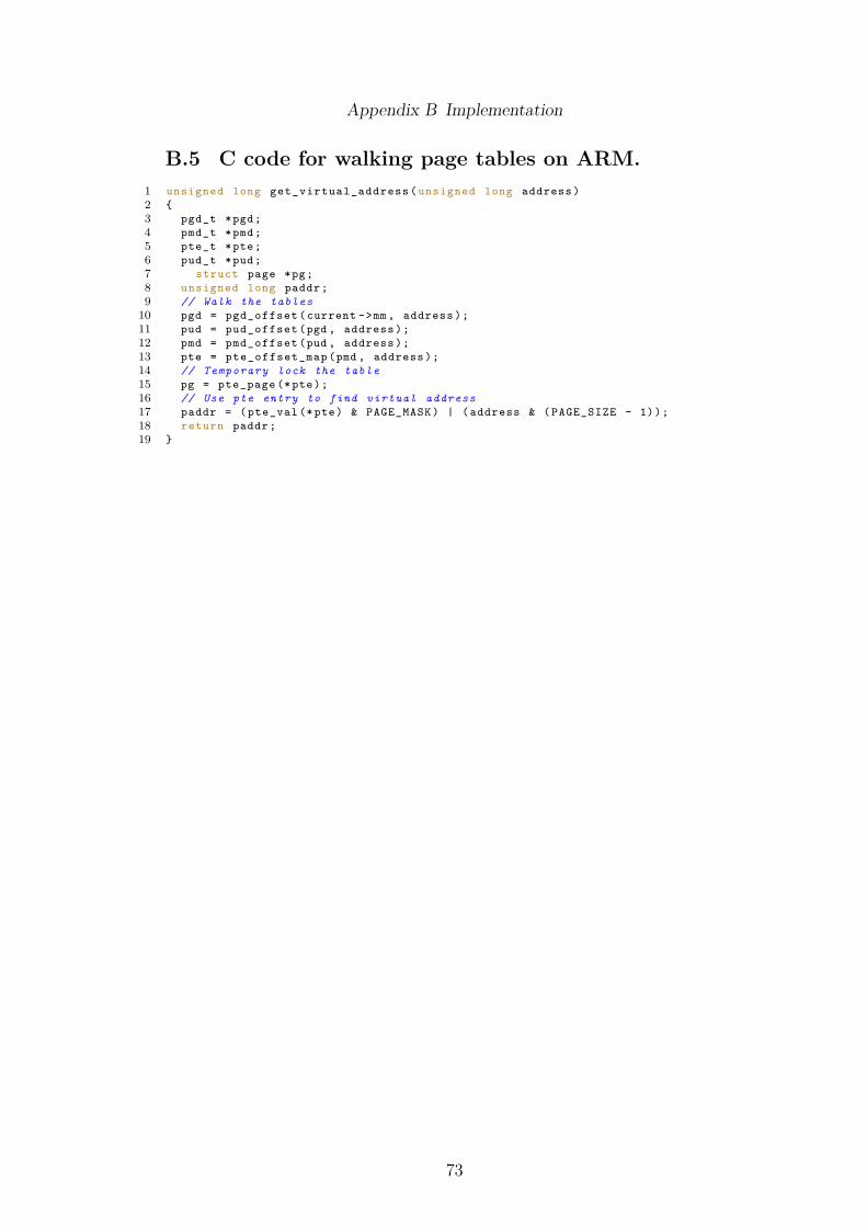
Appendix B Implementation
B.5 C code for walking page tables on ARM.1 unsigned long get_virtual_address ( unsigned long address )2 {3 pgd_t *pgd;4 pmd_t *pmd;5 pte_t *pte;6 pud_t *pud;7 struct page *pg;8 unsigned long paddr ;9 // Walk the tables
10 pgd = pgd_offset (current ->mm , address );11 pud = pud_offset (pgd , address );12 pmd = pmd_offset (pud , address );13 pte = pte_offset_map (pmd , address );14 // Temporary lock the table
15 pg = pte_page (* pte);16 // Use pte entry to find virtual address
17 paddr = ( pte_val (* pte) & PAGE_MASK ) | ( address & ( PAGE_SIZE - 1));18 return paddr ;19 }
73