recent advances in nanorobotic manipulation inside ...amnl.mie.utoronto.ca/data/j131.pdf · open...
TRANSCRIPT

OPEN
REVIEW ARTICLE
Recent advances in nanorobotic manipulation inside scanningelectron microscopesChaoyang Shi1, Devin K Luu1, Qinmin Yang2, Jun Liu1, Jun Chen1, Changhai Ru3, Shaorong Xie4, Jun Luo4, Ji Ge1 and Yu Sun1
A scanning electron microscope (SEM) provides real-time imaging with nanometer resolution and a large scanning area, whichenables the development and integration of robotic nanomanipulation systems inside a vacuum chamber to realize simultaneousimaging and direct interactions with nanoscaled samples. Emerging techniques for nanorobotic manipulation during SEM imagingenable the characterization of nanomaterials and nanostructures and the prototyping/assembly of nanodevices. This paperpresents a comprehensive survey of recent advances in nanorobotic manipulation, including the development of nanomanipulationplatforms, tools, changeable toolboxes, sensing units, control strategies, electron beam-induced deposition approaches,automation techniques, and nanomanipulation-enabled applications and discoveries. The limitations of the existing technologiesand prospects for new technologies are also discussed.
Keywords: automated nanomanipulation; scanning electron microscope; SEM-based nanomanipulation
Microsystems & Nanoengineering (2016) 2, 16024; doi:10.1038/micronano.2016.24; Published online: 20 June 2016
INTRODUCTIONA variety of nanomaterials, such as nanotubes, nanowires, plas-monic and semiconductive nanomaterials, and two-dimensionalmaterials, such as graphene and transition metal dichalcogenides,require their properties to be characterized to understand theirbehaviors and explore their applications in nanoelectronics,nanophotonics, biology, and medicine1–5. The fabrication anddevelopment of nanoscaled devices and nanoelectromechanicalsystems (NEMS) that use these nanomaterials also require precisetechniques for positioning, sensing, and assembly with nanometerresolutions3,6,7.Techniques for constructing nanoscaled devices can be
categorized into top–down, bottom–up, and nanomanipulation-enabled techniques3,7. The top–down approaches typicallyemploy techniques such as X-ray electron beam lithography andnanoimprint lithography8–10. Bottom–up techniques, such as self-assembly, chemical synthesis or super-molecule techniques11,12,are driven by the tendency of physical systems to minimize theirpotential energy. These techniques enable the construction ofstructures and devices via the direct assembly of atoms andmolecules; however, modifying specific locations to adjust thedevice properties can be challenging. Nanorobotic manipulation isa complementary technique that enables flexible maneuveringand precise positioning of nanostructures for nano deviceassembly; it is particularly suitable for device prototyping andproperty tuning3,13. Papers that primarily focused on nanomani-pulation applications and nanomanipulation inside an SEM werepublished in 2008, 2005, and previous years8,13. Conversely, thispaper discusses technological advances and recent discoveriesenabled by SEM-based nanomanipulation in addition to state-of-the-art applications.
The first nanorobotic manipulation experiment was performedby Eigler and Schweizer in 1990 (Ref. 14) with a scanningtunneling microscope (STM) to form the IBM logo by separatelypositioning 35 individual xenon atoms on a nickel substrate at lowtemperatures, which demonstrates atomic-level manipulationand fabrication. However, an STM requires the use of conductiveprobes and samples owing to its working principle7. To mani-pulate different types of materials, an atomic force microscope(AFM), which is a type of scanning probe microscope (SPM),is capable of subnanometer imaging and manipulation15–17.AFMs permit the manipulation of nanoscaled materials in ambient,aqueous, and vacuum environments, which render the techniquecapable of handling conductive, nonconductive, and biologicalmaterials2,18. However, performing simultaneous manipulationand imaging using AFMs remains challenging13,17,19 because theacquisition of one frame of an image by raster scanning requiresat least several minutes. In addition, the look-then-move controlscheme and small scanning area and workspace limit itsmanipulation throughput7,17.A transmission electron microscope (TEM), which emits high-
energy electrons that pass through a sample, is capable ofsubnanometer imaging. With the development of aberrationcorrectors, state-of-the-art TEMs can achieve an imaging resolu-tion of tens of picometers20,21 and perform atomic-level measure-ments for structural dynamics. However, the working principleof TEMs demands special sample preparation, and the smallspecimen chamber and workspace of a TEM limit the capabilitiesof complex nanomanipulation13. Conversely, the SEM detectssecondary electrons that are emitted by the sample surfacewhen struck by an electron beam, which provides real-timenanometer-level imaging7. Compared with TEMs, SEMs have
1Department of Mechanical and Industrial Engineering, University of Toronto, Toronto, ON, Canada M5S 3G8; 2Department of Control Science and Engineering, ZhejiangUniversity, Hangzhou 310058, China; 3Robotics and Microsystems Center, Soochow University, Suzhou 215021, China and 4School of Mechatronic Engineering and Automation,Shanghai University, Shanghai 200072, ChinaCorrespondence: Ji Ge ([email protected]) or Yu Sun ([email protected])Received: 23 February 2016; revised: 2 April 2016; accepted: 5 April 2016
Microsystems & Nanoengineering (2016) 2, 16024; doi:10.1038/micronano.2016.24
www.nature.com/micronano

substantially larger specimen chambers and scanning areas, whichenable the integration of complex nanomanipulation systems.These advantages enable simultaneous imaging and precisenanomanipulation3.A number of nanorobotic manipulation systems have been
constructed for operation inside an SEM since the 1990s8,13,22.Hatamura and Tomomasa pioneered the development of ananomanipulation system inside an SEM23–25. The systemconsisted of two manipulators, a controllable base, a customizedforce sensor, joy sticks, and an optical microscope, which enabledhaptic and position control. Automated pick-and-place of 30 μmspheres inside an SEM was demonstrated24. The system was onlycapable of manipulating relatively large micrometer-sized objectsand was not capable of performing complex assembly tasks owingto the mechanical wobbling of the manipulators and relativelylarge end-effectors.Recently, nanorobotic manipulation platforms with multiple
degrees of freedom (DOFs) and piezoelectric actuators have beenconstructed inside SEMs for manipulating nanoscaled objects withnanometer resolution, which enables the realization of compli-cated tasks that range from mechanical tensile testing andelectrical probing of nanomaterials26–30, electronic and photonicdevice prototyping1,22,31, NEMS assembly31–34, biological cellcharacterization and manipulation3,35,36 and subcellular organelleextraction35,37. State-of-the-art SEM-based nanomanipulationsystems are also integrated with AFMs and focused ion beam(FIB) systems, as well as various tools38 and exchangeabletoolboxes39. With these advances, powerful nano-laboratorieshave been established that are capable of simultaneousimaging, fabrication, and nanomanipulation40–43 with highefficiency and reproducibility via the use of emerging automationtechniques30,44–46.
NANOMANIPULATION SYSTEMS INSIDE SEMSNanomanipulation systems inside SEMs primarily consist of anactuation unit, a sensing unit, control strategies, and nanotools.Techniques such as electron-beam-induced deposition (EBID) areoften employed for nanoscaled welding and assembly. Thissection summarizes recent advances in these technologies.
ActuationActuators that are employed for nanomanipulation inside an SEMmust be compact, vacuum-compatible, and capable of generatingaccurate motions without interfering with electron microscopyimaging. Thermal actuators cannot effectively dissipate heat in avacuum environment, whereas electric motors and voice coilactuators generate magnetic fields that can interfere with electronoptics. Piezoelectric actuators that are governed by the inversepiezoelectric effect overcome these challenges47,48 and arecapable of generating large forces in the kilo-Newton range withsubnanometer positioning resolution and a high bandwidth49. Anumber of piezoelectric actuator-based nanomanipulators withmultiple DOFs have been developed for precise positioning andmanipulation of micro- and nanoscaled objects by companies (forexample, Zyvex, Kleindiek, SmarAct, Toronto Nanoinstrumenta-tion, and Attocube) and academia33,41,42,50–54.The most common configuration of actuators for nanomanipu-
lation is a coarse and fine positioner combination or a singleactuator for both coarse and fine positioning. For instance, Zyvexand Lifeforce systems consist of four quadrants of three-DOFnanomanipulators, each of which uses two separate three-axispiezoelectric actuator units for coarse positioning and fine posi-tioning, respectively, as shown in Figures 1a and b. Thecoarse positioners move according to the slip-stick actuationprinciple49,55 to generate stepwise motions at a high speed andwith total motion ranges on the order of centimeters but with alow resolution and accuracy owing to unrepeatable steps. Theseparate fine unit uses piezo stacks, piezo tubes or flexure-guidedmechanisms47,55 to precisely position the end-effector andenables a large fine motion range on the order of tens ofmicrometers (refer to Table 1). Kleindiek and SmarAct systems arecomposed of four quadrants of three-DOF nanomanipulators,each of which only uses one three-axis piezoelectric actuator unit.The single piezoelectric element either operates as a coarseactuator in the slip-stick mode or operates as a fine actuator solelyin stick mode. This configuration produces a compact designbut can induce undesired vibration during dynamic positioning,and the fine motion range is typically limited to o2 μm.
Figure 1 Examples of commercial nanomanipulation systems. (a) Zyvex. (b) Lifeforce. (c) SmarAct system. (d) Kleindiek.
Nanorobotic manipulation inside SEMC Shi et al
2
Microsystems & Nanoengineering doi:10.1038/micronano.2016.24
In addition to these stationary platforms, mobile nanomanipu-lators have also been developed56–59. Their actuation is typicallybased on the slip-stick principle60 or the inchworm mobilemechanism59 using piezoceramic actuators. These mobile plat-forms perform manipulation with nanometer accuracy. Theycollaborate among multiple robots and are capable of mov-ing longer distances. However, the precise tracking of the posi-tion and orientation of the mobile robots is challenging.Conversely, stationary nanomanipulation platforms can generatemore precise and accurate motion, are easier to control withoutlocalization and coordination difficulties, and facilitate automatednanomanipulation.
SensingAn important consideration for sensing in the vacuum environ-ment is that heat generated from powering sensors cannot beeffectively dissipated, which can cause instability owing to thermaldrift. This section discusses advances in position, depth, and forcesensing that are employed in SEM-based nanomanipulation.
Position sensing. Piezoelectric actuators inherently exhibit non-linear characteristics of hysteresis and creep49, which degradepositioning precision and can cause system instability61. Threetypes of position sensors exist for integration with piezoelectricactuators, including capacitive, optical encoder-based andstrain gauge-based sensors. Although piezoelectric actuatorsinherently possess sensing capabilities for estimating force and/ordisplacement62, piezoelectric self-sensing is difficult to implementin piezoelectric stacks, which is typically employed for theconstruction of nanopositioners.Capacitive sensors provide a noncontact, low-power and direct
position measurement approach for obtaining accuratenanometer and subnanometer measurements with a bandwidthup to 10 kHz and minimum heating63. However, capacitive sensorsare costly and difficult for accurate assembly64 and are limited toshort-range measurements within a couple of millimeters65.Optical encoder-based sensors generate incremental measure-ment readings that are capable of providing accurate positionfeedback for large-motion ranges (for example, tens of milli-meters) at nanometer resolutions41. However, optical elements
generate heat, which can cause thermal drift in surroundingcomponents inside the vacuum chamber of an SEM64. Similarly,strain gauge-based sensors also suffer from thermal driftproblems. When strain gauge-based sensors are utilized for posi-tion sensing inside an SEM, measuring the charging anddischarging time of a capacitor that is connected to a straingauge via time-to-digital conversion has been proven to generate50 times less heat than optical encoders while achievingnanometer resolutions64.
Depth sensing. Height control in nanomanipulation is challen-ging owing to the lack of depth information66–68. Depth sensingcan be achieved using a force sensor to touch a target69.Piezoresistive AFM cantilevers have been applied for heightestimation70. A vibrating piezoelectric bimorph actuator71, inwhich the vibration amplitude decreases upon contact with asubstrate or target, was also demonstrated. Because force sensorsare difficult to integrate with nanomanipulation tools, an image-processing-based approach was developed72. In this approach,after the nanomanipulator tool contacts the target substrate,lowering of the tool causes horizontal sliding, which is detectedby image processing. After the relative vertical position of thenanomanipulation tool relative to the target substrate is detected,closed-loop position control along the Z-direction can beconducted for depth control.Vision-based depth sensing was also realized by installing an
optical microscope and camera to the SEM chamber wall fordetecting tool tip depth73,74. This method’s detection resolution islimited by the Abbe diffraction limit of optical microscopy (that is,hundreds of nanometers). Stereo imaging was employed todetermine tool depth by tilting either the SEM sample stage75,76 orthe electron beam67. Mechanical components in stereo methodsmust be manufactured with tight tolerances, and image driftcompensation must be carefully performed to achieve accuratedepth sensing.
Force sensing. Force sensors provide force feedback innanomanipulation77,78. Microelectromechanical systems (MEMSs)capacitive force sensors utilize comb structures to detect capaci-tance changes that are induced by externally applied forces79,80. A
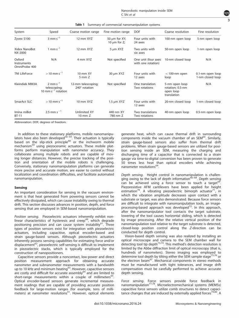
Table 1 Summary of commercial nanomanipulation systems
System Speed Coarse motion range Fine motion range DOF Coarse resolution Fine resolution
Zyvex S100 3 mm s−1 12 mm XYZ 50 μm for XY;10 μm for Z;
Four units with24 axes
100-nm open loop 5-nm open loop
Xidex NanoBotNX-2000
1 mm s−1 12 mm XYZ 5 μm XYZ Two units withsix axes
50-nm open loop 1-nm open loop
OxfordInstrumentsOmniProbe 400
N/A 4 mm XYZ Not specified One unit (four axeswith one rotation)
10-nm closed loop N/A
TNI LifeForce 410 mm s−1 10 mm XY5 mm Z
30 μm XYZ Four units with12 axes
o100-nm openloop
0.1-nm open loop1-nm closed loop
Kleindiek MM3A 2 mm s−1
telescoping;10 mm s−1 rotation
12-mm telescoping;240° rotation
Not specified One translationTwo rotations
5-nm open looprotation; 0.5-nmopen looptranslation
N/A
SmarAct SLC 410 mm s−1 10 mm XYZ 1.5 μm XYZ Four units with12 axes
20-nm closed loop 1-nm closed loop
Imina miBotBT-11
2.5 mm s− 1 Unlimited XY10 mm Z
440 nm XY780 nm Z
Two translationsTwo rotations
40-nm open loop 0.5-nm open loop
Abbreviation: DOF, degrees of freedom.
Nanorobotic manipulation inside SEMC Shi et al
3
Microsystems & Nanoengineeringdoi:10.1038/micronano.2016.24

two-axis MEMS capacitive force sensor81,82 and an improvedsix-axis capacitive force sensor83 were constructed via deepreactive ion etching of silicon on insulator (SOI) substrates. Thesecapacitive force sensors are capable of measuring forces froma few nanonewtons to micronewtons.MEMS piezoresistive force sensors, which are formed by
ion implantation, have also been developed for nanoscaledapplications77,79. Piezoresistive force sensors were mounted on ananomanipulator to provide high-accuracy force measurementsthat range from nanonewtons to millinewtons84. By usingpiezoresistive force sensors, mechanical indentation for stiffnessdetermination of 2D materials and scanning for surface topo-graphy were achieved45.When AFM probes are used for force sensing, an applied force
can be determined from Hooke’s law85,86. The stiffness of an AFMprobe can be calibrated using a reference cantilever of a knownstiffness87. Image processing can be conducted to measure AFMprobe deflections and determine the applied force. In88, vision-based force sensing was achieved using a deformable template-matching algorithm to visually determine the force distributionacts on a linearly elastic object using the contour information in animage. The effectiveness was validated using both AFM probesand microgrippers.
Nanotools and tool exchangersA number of nanotools are employed as end-effectors to performnanomanipulation tasks, such as AFM probes, tungsten needles,and MEMS grippers. AFM probes and tungsten needles are themost popular end-effectors for nanomanipulation owing to theirversatility and commercial availability. A nanomanipulator that isequipped with an AFM probe can perform topography imaging,
indentation, stretching, cutting and pushing, pick-and-placeoperation and assembly, and nanolithography2,8,40,70. The AFMcantilever structure can be modified by FIB etching and depositionto create various types of application-specific tools. For instance,AFM probes were modified to have a flat tip86,89, stiff needletip87,90–93, knife blade tip94 and fork tips95,96 for cellular andintracellular characterization and cell manipulation. Tungstenprobes are fabricated and sharpened by electrochemical etchingto obtain a high-aspect ratio. They were employed to performtensile tests for mechanical characterization97 and pick-and-placeassembly98, as well as electrical characterization of nanoscaledsemiconductor devices and nanomaterials26,30,99.Compared with these single-ended tools, MEMS grippers can be
precisely actuated with large forces to effectively overcomematerial-substrate adhesion and perform reliable grasping of nanoobjects100. MEMS grippers are typically driven by electrostatic,electrothermal, and piezoelectric actuators47,77. They are madewith feature structures using different fabrication methods101–105,and have been applied for various nanomanipulation tasks106–112,as summarized in Table 2. Although electrostatic actuation has lowpower, it requires relatively high actuation voltages. Electrothermalmicrogrippers operate under low voltages, produce short travelranges, and can induce thermal drift to surrounding materials. Thepiezoelectrically driven microgrippers that are reported in Refs.105,113–115 utilized piezoelectric bimorph structures and pro-duced a motion range greater than 20 μm at high actuationvoltages. Sensors can also be constructed in microgrippers forforce-controlled grasping116. Tool exchangers have also beendeveloped for easy replacement of broken tools and themodification of different types of end tools without opening thehigh-vacuum chamber of an SEM. A toolbox array with different tipmorphologies, which are termed Nanobits, was fabricated by
Table 2 MEMS grippers that are used in nanomanipulation
Principle Actuation structure Fabrication Actuation voltage Motion range Usage in nanomanipulation
Electrostatic driven Comb drive DRIE of SOI101,102 Medium voltage ~ 10 μm Pick-and-place of nano spheres and microparticles106–108
Electrothermal driven U-shaped andV-shaped beams
RIE of SOI103 Low voltage ~2 μm Pick-and-place of nanowires109,110;assembly to form customized scanningprobe tips111,112
Piezoelectric driven Bimorph Ultrasonicmachining ofpiezoceramicplates104,105
High voltage 420 μm Manipulation of CNTs, micro grains andcopper spheres105,113–115
Abbreviation: DRIE, deep reactive ion etching; SOI, silicon on insulator.
Figure 2 Control architecture of nanorobotic manipulation inside an SEM; scanning electron microscope.
Nanorobotic manipulation inside SEMC Shi et al
4
Microsystems & Nanoengineering doi:10.1038/micronano.2016.24

electron beam lithography and silicon processing39,117. A micro-gripper detached these tools from the tool array and assembledthem to AFM probes or other end-effectors to form scanning probetips112,117. The commercially available Oxford Instruments OmniP-robe 400 system also features an in situ tool exchange and probetip sharpening for repairing or replacing broken tools.
ControlFor nanomanipulation inside an SEM, a look-and-manipulationscheme can be implemented to accomplish closed-loop control,as depicted in Figure 2. A high-level controller is responsible forsupervising tasks, such as target tracking, trajectory planning, errorhandling, and the parallel execution of subtasks. With multipletypes of sensing modalities (for example, force sensing, depthsensing, and positioning sensing), a sensor fusion approach can beemployed to enhance the success rate of nanomanipulation andprovide a basis for high-level control, decision-making, planningand fault-tolerance handling. A low-level controller receivescommands from a high-level controller to generate driving signalsfor nanopositioning/nanomanipulation.The low-level controller can be implemented via feedback,
feedforward, or feedback–feedforward control61,118,119. A feedfor-ward controller determines control signals according to theknowledge and modes of hysteresis, creep, and vibration. Becausefeedforward control does not rely on sensor feedback for high-bandwidth nanopositioning, the advantages are low cost and lowhardware complexity119,120. In addition, techniques such as inputshaping can be utilized to mitigate vibration121. However, theaccuracy of feedforward techniques is dependent on both themodel and the parameters identified in the model, which canchange over time, especially in dynamic scenarios and the vacuumenvironment inside an SEM122. Feedback control utilizes sensorfeedback, relaxes modeling requirements, and achieves betterperformance in terms of accuracy, vibration suppression, anduncertainty/disturbance rejection61. However, feedback-controllednanopositioning has low bandwidth and requires sensor integra-tion in the hardware platform. Therefore, feedforward- andfeedback-controlled nanopositioning were attempted for higherbandwidth and higher accuracy30.To achieve nanoscaled manipulation and assembly tasks,
control approaches have been developed for tele-operated andautomated nanomanipulation49,123,124. In tele-operated nanoma-nipulation, haptic and visual feedback are usually acquired andpresented to a human operator. The operator sends taskcommands to the nanomanipulators via a joystick or a macro-manipulator. Virtual reality techniques have been introduced toenhance this human-in-the-loop control system by enabling theoperator to feel immersed in the environment based on varioussensory cues125,126. Teleoperation involves significant humanintervention and requires significant operator skills. Tele-ope-rated nanomanipulation is slow and exhibits poor repeatability.For automated nanomanipulation, real-time SEM visual feed-
back is important for providing visual guidance and realizingclosed-loop control. To circumvent challenges such as SEM imagenoise and drift, image denoising and drift compensation methodswere implemented using graphics processing unit (GPU)techniques26,127. SEM tracking algorithms can be classified intofeature-based methods, model-based methods and hybridmethods88,128–132. They are commonly employed to provide ananomanipulation system with visual feedback for automatedoperation.
Electron-beam-induced deposition-assisted techniquesElectron-beam-induced deposition (EBID) is extensively appliedinside SEMs as an important technique to deposit materials forwelding and assembly at the nanoscale42,133–135. EBID involves theintroduction of precursor gases into an SEM chamber from a
nozzle after vaporization or sublimation. The gas molecules aresubsequently irradiated by high-energy electrons, which decom-pose precursor molecules by secondary electrons that arediffracted from the irradiation spot and cause the deposition ofnonvolatile fragments136. Several precursors are available for EBIDto deposit various metals, dielectrics, and semiconductor materi-als, which render this technology a useful assistive technologyfor nanomanipulation, such as bonding end-effectors withmaterials50,137 for pick-and-place operation, soldering differentmaterials for characterization137 and assembly42,134, and sensorinstrumentation138–140. EBID can also be employed to removematerials when oxygen gas is introduced as a precursor141,142.EBID and nanomanipulation were employed to produce high-purity and hybrid metallic nanowires139,143, and various types ofnanowires were grown with the introduction of differentprecursors. For instance, use of a nanomanipulator to preciselycontrol the distance between a multi-walled CNT (MWCNT) field-emitter cathode and a tungsten probe emission anode, a high-purity platinum nanowire for intracellular PH sensing was formedusing EBID with the introduction of trimethylcyclopentadienylplatinum (CpPtMe3) as a precursor139.
Hybrid system integration inside SEMsThe large chambers of SEMs enable other microscopy andmanipulation instruments to be integrated and form a hybridsystem. These hybrid systems include AFM/SEM, AFM/FIB/SEM,STM/SEM, AFM/ESEM, and SEM/TEM, which take advantage ofthe strength of each tool for performing characterization andnanomanipulation tasks. Table 3 summarizes and compares thesehybrid systems.SEM and AFM are complementary techniques for performing
topography and morphology measurements16,144,145. The inte-gration of an AFM inside an SEM enables simultaneous imagingand manipulation in real-time to perform SEM-guided topo-graphy analysis with high-resolution and force feedback. FIBhas also been integrated for material etching and deposition.Several hybrid AFM/SEM and AFM/FIB/SEM systems have beendeveloped28,40,43,146,147, and commercial systems have alsobecome available (for example, Semilab, Attocube, Trioptics,Nanonics Imaging Ltd, Kleindiek Nanotechnik).Conventional AFM is based on laser beam deflection and is not
typically integrated inside SEMs owing to space and optical pathconstraints. A commercial hybrid AFM/SEM system by DME-SPMSemilab was designed with modified laser paths inside an SEM, asshown in Figure 3a. Attocube Systems AG uses a fiber-opticconfiguration to construct an in situ AFM for operation inside anSEM (attoAFM/SEM) with a laser interferometer (Figure 3b). Forthese laser-based methods, laser alignment must be carefullyperformed, and low laser power must be maintained to mitigatethermal drift in the vacuum chamber of an SEM.Conversely, laser-free AFM that uses self-sensing cantilevers and
tuning forks can be readily integrated inside an SEM. The AFM/SEM system reported in Ref. 43 employed piezoresistive cantileversto perform scanning and manipulation tasks with force feedback,as shown in Figure 3c. Dynamic AFMs that use a tuning fork with aQPlus or Akiyama probe were also integrated inside an SEM toscan samples that are especially susceptible to surface damage148.A dynamic AFM was integrated inside an SEM by Trioptics torealize surface topography with a large scanning area of 500 by500 μm (Figure 3d). The 3TB4000 system from Nanonics ImagingLtd. is an instrument that integrates an AFM, which is based on atailor made Q-Plus tuning fork, an SEM and an FIB, as shown inFigure 3e. This hybrid instrument enables imaging with a largefield of view from an SEM, three-dimensional (3D) material andend tool modifications with FIB, and high-resolution AFM imaging.Figure 3f shows another hybrid AFM/FIB/SEM system that uses
Nanorobotic manipulation inside SEMC Shi et al
5
Microsystems & Nanoengineeringdoi:10.1038/micronano.2016.24

piezoresistive cantilevers in contact mode AFM imaging andmanipulation with SEM imaging and FIB etching/deposition40.STM/SEM integrated systems have also been developed for
simultaneous imaging, manipulation, and measurements149,150. Ahybrid system that consists of a four-probe STM and an SEM that iscoupled to a molecular-beam epitaxy sample preparationchamber was developed for four-point electrical measurementsand nanomanipulation of individual atoms to nanowires150,151.Both TEMs and SEMs work in high-vacuum conditions. There-
fore, water-containing samples cannot be directly observedinside an SEM or TEM152,153. Environmental scanning electronmicroscopes (ESEMs) overcome this limitation and permit theobservation of liquid-phase materials, such as biological cellswithout metal coating and other electrically insulating materialsthat use a special secondary electron detector86,154.The first hybrid AFM/ESEM system was developed for accurate
topography measurements and tip–sample interactionobservations52,155. Although ESEM’s imaging resolution is typicallylimited to a few nanometers, the integrated AFM achieved aresolution better than 0.2 nm in both contact mode AFM imagingand noncontact mode AFM imaging52. The nanomanipulationsystem that was reported in Ref. 90 was constructed inside anESEM, which consists of two units for manipulation with sevenDOFs and one cooling stage for holding samples and sampletemperature control. This system performed simultaneous real-time observation and manipulation of biological samples for cellproperty characterization and surgery87,91,95,156.To prepare the TEM samples, a hybrid nanomanipulation system
that was integrated with an eight-DOF manipulator and a six-DOFmanipulator inside an SEM and a TEM, respectively, was cons-tructed3,13,153, as shown in Figure 3g. Samples were manipulatedand prepared by the SEM manipulator onto the TEM manipulator/holder inside the SEM chamber and subsequently transferred tothe TEM for observation and measurement153.
STATE-OF-THE-ART APPLICATIONSThis section discusses the applications enabled by nanomanipula-tion inside an SEM, including the characterization of themechanical and electrical properties of nanoscaled materials andstructures, the assembly of nanodevices (for example, biochemicalsensors and nanoelectronics and nanophotonics devices), single-cell manipulation and subcellular organelle extraction, and 3Dnanoscaled structural reconstruction of organelles.
Manipulation and characterization of nanomaterialsAn individual MWNT was EBID-fixed on an AFM cantilever viananomanipulation to determine the MWNT’s Young’s modulus42,as shown in Figure 4a. Mechanical characterization of one-dimensional nanomaterial was also conducted via tensile testingby two AFM cantilevers50,137. Using this approach, Zhu et al.conducted in situ tensile testing of a silver nanowire for mecha-nical characterization of its Young’s modulus, yield strength, andultimate tensile strength51, as shown in Figure 4b. An InGaAs/GaAsnanospring was stretched for tensile tests using a similar methodto determine its stiffness157,158 (refer to Figure 4c).Figure 4d shows an example of the characterization of 2D
nanomaterials, where 2D nanopaper composed of microfibrillatedcellulose was fixed on both ends and driven against a capacitiveforce sensor probe to perform nanoindentation159. Figure 4eshows the indentation of a graphene film using a piezoresistiveAFM cantilever. The graphene film was transferred to be suspen-ded on a standard aluminum TEM grid28,45. Characteristic force-displacement curves were collected during the indentationprocess, and the Young’s modulus of the graphene films wasdetermined160. Figure 4f shows non-destructive measurementusing a tuning fork-based end-effector on a batch of suspended
Table3
Summaryofhyb
ridsystem
s
Hyb
ridsystem
sConfiguration
Endeffectors
Functions
Limitations
AFM
/SEM
Optics-based
AFM
cantilevers
Allavailable
AFM
modes
(forexam
ple,D
ME-SP
MSe
milab,A
ttocu
be)
Thermal
drift
Optics-free
Contact
mode
Piezoresistivecantilevers
Scan
ningan
dman
ipulationwithforcefeed
back4
3Piezoresistivecantilevers
only
Dyn
amic
mode
Tuningfork-based
probes;A
kiyamaprobe
Scan
ningforultrasensitive
surfacetopography1
48
Noman
ipulationfunctions
AFM
/FIB/SEM
Optics-free
Contact
mode
Piezoresistivecantilevers
Fabrication,scanningan
dman
ipulationwithforce
feed
back4
0Piezoresistivecantilevers
only
Dyn
amic
mode
Tuningfork-based
probes;A
kiyamaprobe
Fabricationan
dsurfacetopography(forexam
ple,
Nan
onicsIm
agingLtd)
Noman
ipulationfunctions
STM/SEM
Optics-free
Tungsten
probes;C
onductiveAFM
probes
Scan
ningwithcu
rren
tfeed
backat
both
low
androom
temperatures1
50,151
Conductiveprobes
only
AFM
/ESE
MOptics-based
AFM
cantilevers
AllAFM
modes
available,e
specially
forbiological
samples5
2Th
ermal
drift
SEM/TEM
TEM
holder
withpiezo
actuators
Nolim
itations
Sample
preparationin
SEM,a
ndman
ipulationin
TEM
153
Smallw
orkspaceinsideTE
M
Abbreviations:AFM
,atomic
forcemicroscope;
SEM,scanningelectronmicroscope;
STM,scan
ningtunnelingmicroscope;
TEM,tran
smissionelectronmicroscope.
Nanorobotic manipulation inside SEMC Shi et al
6
Microsystems & Nanoengineering doi:10.1038/micronano.2016.24

InP membranes to determine their stiffness values148. The tuningfork with a QPlus probe was controlled in frequency modulationmode, and the frequency shift was measured to calculate thesample stiffness161.Nanomanipulation was also applied to conduct electrical
characterization of nanomaterials. Figure 4g illustrates piezo-resistivity characterization of a Si nanowire under tensile strain.The Si nanowire’s two ends were anchored on a cantilever and an
insulated Si pad, respectively. One probe, which was labeled ingreen in Figure 4g, was used to apply stress to the freestandingcantilever, which generated strain on the Si nanowire. Thetwo probes labeled in red were controlled to form electricalconnections to measure the nanowire’s electrical resistancechanges162. For the electrical characterization of graphene, anL-shaped four-point probe was fabricated using FIB and controlledto probe a graphene film28, as shown in Figure 4h. Nanoprobing
Figure 3 Hybrid system integration inside an SEM. (a) A hybrid AFM/SEM system based on laser beam deflection by DME-SPM. (b) AttoAFM/SEM system with a fiber-optic configuration by Attocube Systems AG. (c) A hybrid AFM/SEM system using self-sensing piezoresistivecantilevers. Adapted from Ref. 43. (d) An AFM system in dynamic mode for SEM integration by Trioptics. (e) 3TB4000 AFM/FIB/SEM systemfrom Nanonics Imaging Ltd. (f) A hybrid AFM/FIB/SEM system. Adapted from Ref. 40. (g) A hybrid SEM and TEM manipulation system.Reprinted with permission from Ref. 13. AFM, atomic force microscope; FIB, focused ion beam; TEM, transmission electron microscope.
Figure 4 Examples of applications involving mechanical and electrical manipulation and characterization of nanostructures. (a–c) Mechanicalcharacterization of MWNTs, nanowires and nanosprings. Adapted from Refs. 42,51,157. (d–f) Mechanical characterization of 2D materialsof nanopapers, graphene films and suspended InP membranes using nanoindentation and contactless measurements. Adaptedfrom Refs. 148,159,160. (g–i) Electrical characterization for nanowires, graphene flakes and single transistors on IC chips. Adapted fromRefs. 28,162.
Nanorobotic manipulation inside SEMC Shi et al
7
Microsystems & Nanoengineeringdoi:10.1038/micronano.2016.24

inside SEM was also employed to attain I–V data of singletransistors on IC chips by Kleindiek Nanotechnik (refer toFigure 4i), for identifying faulty locations and understandingfailure mechanisms27.
Assembly of nanodevicesWith its precise positioning and manipulation capabilities,nanorobotic manipulation has enabled the assembly of nanos-tructures and nanodevices. Figure 5a shows that individual goldnanowires were picked and placed by two nanoprobes andsubsequently welded and assembled to form the nano pattern‘NANO’163. A 3D letter ‘N’, as shown in Figure 5b, was formed byEBID with oxygen as a precursor for cutting and bending of aMWCNT and nanomanipulation for assembly13,141,164. Figure 5cshows a thermal sensor that is composed of two MWCNTsassembled on an AFM cantilever with EBID and nanomanipu-lation138. In Figure 5d, two nanotubes were successively manipu-lated and assembled to form a pair of nanoscaled tweezers165. ADC voltage was applied to open and close the nanotweezers forthe pick-and-place of nanoparticles.A 3D pyramidal structure that consists of stacked silica spheres,
as shown in Figure 5e, was assembled via cooperative manipula-tion using two nanoprobes. A tungsten nanoprobe and a modifiedpiezoresistive AFM cantilever with a spherical adhesion pocket tipwere employed to pick and place the silica spheres70. In Figure 5f,a custom nanotip was manipulated by a microgripper to approachan AFM cantilever and subsequently soldered and assembled ontothe AFM cantilever tip using EBID to construct a high-aspect-ratioAFM cantilever tip for high-resolution imaging39. To produce a 3Dphotonic crystal device (Figure 5g2)1, a thin plate was separatedfrom a substrate after the connection bridge was broken with ananoprobe and picked and transferred for assembly, as shown inFigure 5g1.
Nanorobotic manipulation also enabled the assembly of a varietyof other NEMS devices7,22,166,167 for applications in the nanoelec-tronics and bionanotechnology sectors, as summarized in Table 4.
Cell characterization and manipulationStandard AFM cantilevers were modified using FIB etching anddeposition to produce different types of functional tools, suchas a soft buckling nanoneedle86,90,91, a nano-fork and a nanoputter95,168, as shown in Figures 6a, b and c, respectively. Thesetools were mounted on a nanomanipulation system in ESEM toperform indentation to determine cell stiffness and viscoelasticproperties87,90. The nanomanipulation system was also employedto lift and push a cell to measure adhesion forces between the celland substrate89,95,156,168; to measure cell–cell adhesion force96;and to electrically characterize intracellular properties36, as shownin Figures 6d and e. Figure 6f shows the use of a nano-knife forperforming cell surgery of a yeast cell94. The extraction of DNAfrom a single-cell nucleus was performed via nanomanipulationunder SEM. A nanomanipulation system equipped with ananospatula as the end-effector was employed to dissect andcollect a single-chromatin complex from within a cell nucleusafter correlating SEM images and fluorescence microscopy imagesto determine the target locations to extract169, as shown inFigures 6g1–g3. Because gene locations within the nucleus are notrandom, this technique enables high-throughput gene mappingfor exploring gene loci associations with nuclear substructures37.
Automated nanomanipulationManual nanomanipulation by a joystick is time-consuming andskill dependent. Over the past decade, progress in auto-mated nanomanipulation tasks has been achieved49,170. Table 5summarizes representative automated nanomanipulation. Themajority of automated SEM-based nanomanipulation tasks were
Figure 5 Examples of nano device and nanostructure assembly. (a) Nanowires were picked and placed to assemble a nano pattern. Adaptedfrom Ref. 163. (b) A MWCNT was formed using a 3D letter with EBID. Adapted from Ref. 13. (c and d) A thermal sensor and a pair of nanoscaledtweezers were assembled with nanomanipulation. Reprinted with Institute of Physics Publishing (IOP) permission from Ref. 138 and adaptedfrom Ref. 165. (e) 3D pyramidal spheres were assembled. Adapted from Ref. 70. (f) A nanotool was mounted on an AFM cantilever. Reprintedwith IOP permission from Ref. 39. (g1 and g2) Assembly of photonic plates to form a 3D photonic crystal. Adapted from Ref. 1. EBID, electron-beam-induced deposition; MWCNT, multi-walled CNT.
Nanorobotic manipulation inside SEMC Shi et al
8
Microsystems & Nanoengineering doi:10.1038/micronano.2016.24

performed with custom instruments using piezoelectric posi-tioners. AFM cantilevers, tungsten probes and MEMS grippers withEBID-assisted soldering techniques are employed for assemblyand pick-and-place operation, primarily via SEM-based visualservoing and assisted by force and depth detection. Developingthe non-application-specific automated nanomanipulation solu-tions remains challenging.
Automated pick-and-place of nano objects. In Ref. 112, a MEMSgripper was controlled to automatically pick up a CNT from a
substrate and place and solder it onto a target structure. Depth-from-focus and depth detection using a piezoelectric touch sensorwere employed for coarse and fine alignment to place themicrogripper with respect to the CNT in the Z-direction for pick-up71. A manipulation strategy using line and two-point contact toadjust adhesion forces was developed to place the CNT onto atarget AFM tip to form a CNT-enhanced, high-aspect-ratio AFM tipfor scanning deep trenches112. For mechanical characterization,individual silicon nanowires were automatically picked up andplaced on a MEMS tensile testing device98,171. Via visualrecognition and vision-based closed-loop control, a nanowirewas picked up from the growth substrate and moved for fixationon the MEMS device with EBID. Automated pick-and-place ofindividual colloidal spheres was realized using two nanoprobeswith tailored geometries for cooperative manipulation to form a3D pyramidal structure via visual servoing and force control70. Themethod did not involve the use of EBID and provided a flexiblestrategy for 3D nano assembly.
Automated nanoprobing. Nanomanipulation is capable of auto-mated positioning of nanoprobes on nanostructures to performelectrical characterization for fault analysis and quality control.Automated nanoprobing was performed to probe nanostructureson SEM metrology chips, as shown in Figures 7a and b. Algorithmswere developed on a GPU to realize real-time SEM imagedenoising and drift compensation, which enable robust visualtracking and visual servo control for automated nanoprobing26,27.Automated four-point probe measurements on single nanowireswere also performed for electrical characterization30, as shown inFigure 7c, where four tungsten nanoprobes were moved
Table 4 Nanoelectromechanical systems (NEMS) constructed bynanomanipulation inside SEM
NEMS Types References
Nanotube-based Nanoactuator Linear motor 22,31,42Linear bearing 42,166
Nanosensor Thermal sensor 138Mass flow sensor 42
Nanotool Nanotweezers 165Nanoscissors 42SPM probes 112,133Field emitters 133,139
Nanowire-based Nanosensor Gas sensor 40Nanotool Transistors 32,40,167
Graphene-based Nanosensor Oscillator 28
Abbreviations: NEMS, nanoelectromechanical systems.
Figure 6 Cell characterization and manipulation inside an ESEM and SEM. (a) Cell stiffness measurement. Adapted from Ref. 90. (b–d) Cell–substrate and cell–cell adhesion force determination. Adapted from Refs 89,95 and reprinted with IOP permission from Ref. 96. (e) Intracellularelectrical measurement for viability testing. Adapted from Ref. 36. (f) Single cell cutting. Reprinted with IOP permission from Ref. 94. (g1–g3)Chromatin extraction process. Adapted from Ref. 37.
Nanorobotic manipulation inside SEMC Shi et al
9
Microsystems & Nanoengineeringdoi:10.1038/micronano.2016.24

downward to contact the substrate via a vision-based contact-detection method72 and subsequently moved upward to a certainheight above the substrate. Via visual servo control with afeedforward controller69,172, the four probes were positioned viaclosed-loop control to land on their respective target locationsalong the nanowire at a pre-defined separation distance. The I–Vcharacteristics of the nanowire with regard to different separationdistances between the two inner probes are shown in Figure 7d.
SEM-guided, automated AFM manipulation. SEM imaging can beemployed to guide the AFM cantilever to localize the regions ofinterest where AFM imaging or measurement is conducted. Ahybrid AFM/FIB/SEM system that employed a piezoresistivecantilever was controlled to realize automated indentation formechanical characterization of graphene membranes45. Thepiezoresistive cantilever provided force feedback, and a calibra-tion cross-structure by FIB milling was created on its back surfaceto enable reliable visual tracking of the cantilever. Graphenemembranes were automatically picked up and transferred tosuspend on a substrate with a grid pattern, as shown in Figure 7e.SEM imaging was utilized to detect the cantilever position and thecenters of holes in the pattern and guide the cantilever to performnanoindentation at the detected centers (Figures 7f and g).Indentation depths and applied forces, as shown in Figure 7h,were measured for determining the Young’s modulus values ofthe graphene membranes.
3D image reconstruction by nanotomographyUltramicrotomy involves serially cutting and imaging thin slices ofa sample under an SEM. It has served an important role instudying the anatomy of cells and tissues in histology andtomography in materials science173. In 2004, Denk and Horstmannpresented serial block face scanning electron microscopy(SBFSEM)174, which is a nanomanipulation method for automati-cally sectioning and 3D reconstructing of tissue structures. Themicrotome inside an SEM consisted of a moving diamond knife forslicing a sample and an actuator/positioner to advance thespecimen after each slice. After each slicing, the remaining blockface was imaged174. Algorithms for image segmentation andstructural reconstruction were developed to generate a 3D tissuenanostructure of biological and other material specimens from theserial images with nanometer resolutions76.The development of SBFSEM has enabled advances in
neuroscience, in which previous studies have either focused ondetailed small volumes or averages over large volumes. SBFSEMbridges the gap by enabling the tracing of neuronal networks andrevealing synaptic connections with nanometer resolutions overvolumes as large as 1 mm3 (Ref. 175). The technique is sufficientlyfine to resolve morphologies of structures, which can provideclues to their function for a better understanding of certainpathologies. Study tissues that involve long tissue fibers canparticularly benefit from SBFSEM. The technique has also beenapplied in materials science to study the microstructure ofengineered materials176.
DISCOVERIES ENABLED BY SEM-BASED NANOMANIPULATIONLeveraging the technical advances in SEM-based nanomanipula-tion, many fundamental discoveries have been made, some ofwhich are summarized in Table 6. Mechanical characterization ofnanomaterials has significantly benefited from SEM in situnanomanipulation. For instance, nanomanipulation and tensiletesting of Ag nanowires of different diameters revealed quantita-tively the size and structure effects on the nanowire’s mechanicalproperties (that is, Young’s modulus, yield strength, and ultimatetensile strength)51. Nanomanipulation was also conducted toperform measurements on silicon nanowires177 and CNTs50,137 to
Table5
Summaryofau
tomated
nan
oman
ipulation
Task
Nan
otool
Feed
back
Object
size
Successrate
Throughput
Referen
ces
Pick-and-place
ofparticles
Twoen
d-effectors
form
edonan
AFM
cantileve
rSE
M-based
visual
servoing;
capacitivepositionsensors;
piezoresistiveAFM
cantileve
rforco
ntact
force
detection
1160
nm,
519nm,
237nm
100%
for10
0particles
112sper
particle
70
Pick-and-place
ofnan
owire
Electrothermal
MEM
Sgripper;
SEM-based
visual
servoing;
piezo
bim
orphtouch
sensorfordep
thsensing
30–15
0nm
Notreported
Notreported
71
Tungsten
probes
SEM-based
visual
servoing
74–11
3nm
Notreported
10min
per
nan
owire
98
Pick-and-place
fornan
otool
assembly
Electrothermal
MEM
Sgripper;
FIBmodified
AFM
cantileve
r
SEM-based
visual
servoing;
opticalen
coder
3–4-μm
long,
150-nm
thick
Notreported
Notreported
39
Nan
oprobingofnan
ostructures
Tungsten
probes
SEM-based
visual
servoing
130nm
Notreported
15.3
sper
2locations
26
Nan
oprobingofnan
owires
Tungsten
probes
SEM-based
visual
servoing;
vision-based
contact-detection
70–10
0nm
100%
for50
measuremen
ts20
sper
nan
owire
30
Mem
braneinden
tation
PiezoresistiveAFM
cantileve
rSE
M-based
visual
servoing;
piezoresistiveinden
tationforcesensing;
capacitivepositionsensors
50-nm
thick
Notreported
Notreported
45
IntracellularDNAextraction
Nan
ospatula
SEM-based
visual
servoing;
strain
gau
ges
forposition-sen
sing
100nm
16%
Notreported
37
Abbreviations:AFM
,atomic
forcemicroscope;
FIB,
focu
sedionbeam;S
EM,scanningelectronmicroscope.
Nanorobotic manipulation inside SEMC Shi et al
10
Microsystems & Nanoengineering doi:10.1038/micronano.2016.24

Figure 7 Automated nanomanipulation. (a and b) Automated nanoprobing. Adapted from Ref. 26. (c and d) Automated four-point probemeasurement on a single nanowire. Adapted from Ref. 30. (e–h) SEM-guided AFM stiffness measurement of graphene. Adapted from Ref. 45.
Table 6 Examples of discoveries enabled by nanomanipulation inside an SEM
Technique Field of discovery Discovery References
Mechanical testing Nanomaterials Young’s modulus, yield strength, and ultimate tensile strength of Ag NWsincreased as the diameter decreased. Yield strain scaled with surface area, andyielding was caused by dislocation nucleation from surface sources. Thepronounced strain hardening was primarily attributed to the presence of internaltwin boundaries.
51
Lithium-ion battery The delithiated Si nanowire exhibited a significant decrease in the elastic modulusand the ultimate tensile strength owing to the newly formed amorphous Si layers.
178
Electrical nanoprobing CMOS manufacturing Strained Si nanowires revealed the positive piezoresistance effect at a low strainlevel of o0.8%, whereas an anomalous negative piezoresistance effect andfatigue failure were not observed after several hundred loading cycles for high-strain levels.
162
Nanomaterials Large discrete resistance jumps were measured at the random grain boundaries(GBs) in copper nanowires. A metal− insulator transition is revealed in GdSi2quantum nanowires, whereas a robust metallic state is obtained in wire bundles atlow temperatures. The strain effect has served an important role dynamic phaseevolution for both phase separation and Mott metal–insulator transition owing tostrong electron-lattice coupling.
150,179,180
Semiconductor A variation in threshold voltage for each type of cell transistor was normaldistribution; marginal failures or degradations that relate to the ultrathin gateoxides, variations in the resistance of the implanted layers in the substrate, and anabnormal passive-voltage-contrast signature were determined.
27
Cellular dissection Cell biology Four new gene loci were associated with promyelocytic nuclear bodies, which aretumor-suppression proteins in humans.
37
Cellular characterization Cell biology A time effect on yeast cell–cell adhesion force was observed: The force rose toapproximately 25 nN with an increase in contact time for the first few minutes andsubsequently attained a balance condition with constant force. The stiffness of asingle cell decreases with increasing humidity.
93,96
SBFSEM Neuroscience Postsynaptic membrane of the predominant synaptic connections were reinforcedwith use to form a permanent connection, whereas other axons are pruned.
182
Neuroscience Synaptic pruning does not proceed normally in the absence of bonemorphogenetic proteins, and synapses remain multiply innervated.
183
Cell biology A previously unknown ridge-like structure on podocytes was discovered, whichchanged the understanding of podocyte anatomy.
186
Abbreviations: CMOS, complementary metal-oxide semiconductor; NW, nanowire; SBFSEM, serial block face scanning electron microscopy.
Nanorobotic manipulation inside SEMC Shi et al
11
Microsystems & Nanoengineeringdoi:10.1038/micronano.2016.24

understand how their properties change with size and structurevariations. Nanomanipulation and mechanical measurements alsoshed light on the degradation process of silicon nanowire anodesin lithium-ion batteries178, contributing to the optimization ofbattery electrode design for enhanced reliability.Nanomanipulation and electrical characterization of strained Si
nanowires revealed the positive piezoresistive effect at low strainlevels and also found carrier mobility enhancement for strainedSi-CMOS (silicon-complementary metal-oxide semiconductor) insemiconductor devices162. At high-strain levels, the negativepiezoresistive effect became apparent, and no fatigue failuresoccurred after several hundred loading cycles. These findingsemphasize the importance of crystallinity and strain for Sinanowires in semiconductor applications162.SEM in situ electrical characterization of GdSi2 quantum
nanowires explained how the electronic transport nature ismodified by local atomic defects and interwire coupling in aquantum wire system179. The atomic defects produce electronlocalizations in isolated nanowires, and interwire couplingstabilizes the structure and promotes the metallic states in wirebundles180. For IC testing at the transistor level, electricalcharacterization by nanoprobing inside an SEM was performedto evaluate SRAM cells for failure analyses, which revealed the rootcauses and failure mechanisms27 and contributed to the packa-ging and IC-MEMS integration181.Intracellular dissection via nanomanipulation inside an SEM
extracted target DNA from a single-cell nucleus to discover geneassociations with nuclear bodies37. Four new gene loci onchromosomes 11, 17, and 18 that have a significant associationwith promyelocytic leukemia nuclear bodies, which are tumor-suppression proteins in humans, were discovered. Known geneloci on chromosomes 1 and 6, which are associated with histonelocus bodies, were reconfirmed; this finding proves that nano-dissection is a viable method for discovering mechanisms fornuclear event regulation. Nanomanipulation of cellular materialsrevealed how chemical bonds regulate cell–cell adhesion and itscontact-time dependence96.SBFSEM was employed to study neuronal circuit develop-
ment182. When new synapses are formed, they are innervated bymany axons. During development, the connections carry compet-ing signals, and the axon with the strongest signal remainsconnected, while the remaining axons withdraw in a process thatis referred to as synaptic pruning or synapse elimination. UsingSBFSEM, the postsynaptic membrane of an axon that carries the‘winning’ signal was reinforced. SBFSEM was also employed toinvestigate the role of bone morphogenetic proteins (BMPs) insynapse generation and development183. In the absence of BMPs,synapse elimination at the calyx of Held in a mouse brain did notoccur normally, whereas control mouse neurons undergo normalsynapse elimination in the presence of BMPs. Studies havesuggested that abnormal synapse elimination may be a risk factorfor neurological or psychological diseases184,185. The structure ofpodocytes, which is a type of cell in kidneys that filters blood186,were also examined using SBFSEM. Three different structures,including the cell body, the primary process, and the foot process,were previously identified. However, the SBFSEM data discoveredridge-like structures on which the foot processes are anchored.These ridge-like structures appear on both the primary processand the cell body; this discovery changes a misunderstanding ofpodocyte anatomy.
SUMMARY AND OUTLOOKThis paper presented technical advances in the establishmentof nanorobotic manipulation laboratories inside SEMs forsimultaneous imaging and nanomanipulation. These platformsand nanomanipulation techniques have enabled the in situcharacterization of nanomaterials, the assembly of nano device
prototypes, and the analysis of subcellular organelles. Despite thesignificant progress that has been achieved in the past twodecades, challenges remain in the realization of 3D nanomanipu-lation with high precision, robustness, flexibility, and highthroughput.The majority of SEM-based nanomanipulation tasks are
manually performed. Although a number of sensing technologieshave been developed for integration into nanomanipulationsystems, automation remains dependent on SEM imaging asfeedback. The low frame rate of SEMs and the high noise, drift,and distortion of real-time SEM imaging hinder the achievementof reliable visual tracking and pose estimation of end-effectorsand target objects for high-speed nanomanipulation. Advancedvisual tracking methods must be developed to cope with blurredand distorted SEM images. Advanced control schemes thatemploy integrated information from image-, force-, depth-, andposition-sensing modalities are needed for effective decision-making, planning, and manipulation.During the past decade, efforts have been made in automated
nanomanipulation (for example, pick-and-place of CNTs44 andnanowires for mechanical characterization98, nanowire field-effecttransistor assembly32), nanoprobing for electrical characterizationof nanowires and transistors26,30, and SEM-guided AFM mani-pulation for the transfer and stiffness measurement of graphenemembranes28,45. Automated nanoprobing has demonstratedhigher consistency and at least three times faster operation thanmanual operation26, in addition to minimizing the risks ofnanotools and sample breakage30. Automated pick-and-place ofnanowires was completed within 10 min compared with 2 h byteleoperation98,171. Although techniques such as visual tracking,depth detection, and the integration of feedback and feedforwardcontrol for piezoelectric positioning have been developed forautomated nanomanipulation in known environments, systemperformance may deteriorate in changing environments withuncertain physical parameters and dynamic disturbances.The application of nanomanipulation has penetrated several
disciplines and sectors, such as materials science, semiconductor,cell biology, and neuroscience. Some notable achievements aremechanical and electrical characterization of graphenemembranes28,45, electrical measurement of single transistors27,3D transfer of graphene28,45, assembly of photonic crystaldevices1,187, identification of the size effect on the mechanicalproperties of nanowires and the strain effect on the piezoresistiveproperties of nanowires51,162, discovery of new gene lociassociated with promyelocytic nuclear bodies37, and tracing ofneuronal networks and synaptic connections182,183.The formation of hybrid systems by integrating other instru-
ments into an SEM has also produced unique capabilities. Forinstance, STM/SEM integration is capable of manipulating indivi-dual atoms; characterizing electrical transport of CNTs, bending,and cutting nanofibers; and fabricating nanowires151,188. Thisintegration has also enabled fundamental discoveries of intrinsicstructure-transport at the atomic scale180 and the effect of appliedstress on dynamic phase evolution189. In addition to STM,nanoscale laboratories inside an SEM have also integrated AFM,FIB, optical microscopes, and multi-tool changers. Furtheradvances in hardware development will produce powerful in situcapabilities for manipulation, assembly, and characterization ofnanoscales objects and materials to close the gap betweencurrent bottom–up and top–down technologies.With the unique advantages of programmability, automation,
and specificity, nanomanipulation inside an SEM will continue toserve as a strong driver of scientific discoveries and further evolveinto a more powerful workhorse technology for the nano sciencesand nanotechnology industries.
Nanorobotic manipulation inside SEMC Shi et al
12
Microsystems & Nanoengineering doi:10.1038/micronano.2016.24

ACKNOWLEDGEMENTSThis study was supported by the Natural Sciences and Engineering Research Councilof Canada, the Canada Research Chairs Program, and the Ontario Ministry of Researchand Innovation via an ORF-RE grant.
COMPETING INTERESTSThe authors declare no conflict of interest.
REFERENCES1 Aoki K, Miyazaki HT, Hirayama H et al. Microassembly of semiconductor three-
dimensional photonic crystals. Nature Materials 2003; 2: 117–121.2 Garcia R, Knoll AW, Riedo E. Advanced scanning probe lithography. Nature
Nanotechnology 2014; 9: 577–587.3 Fukuda T, Nakajima M, Ahmad MR et al. Micro-and nanomechatronics. IEEE
Industrial Electronics Magazine 2010; 4: 13–22.4 Liu J, Wen J, Zhang Z et al. Voyage inside the cell: Microsystems and nanoen-
gineering for intracellular measurement and manipulation. Microsystems &Nanoengineering 2015; 1: 15020.
5 Yost AL, Shahsavari S, Bradwell GM et al. Layer-by-layer functionalized nanotubearrays: A versatile microfluidic platform for biodetection. Microsystems &Nanoengineering 2015; 1: 15037.
6 Requicha AAG. Nanorobots, NEMS, and nanoassembly. Proceedings of the IEEE2003; 9: 1922–1933.
7 Dong L, Nelson BJ. Tutorial—robotics in the small Part II: Nanorobotics. IEEERobotics & Automation Magazine 2007; 14: 111–121.
8 Fahlbusch S, Mazerolle S, Breguet JM et al. Nanomanipulation in a scanningelectron microscope. Journal of Materials Processing Technology 2005; 167:371–382.
9 Esashi M, Kojima A, Ikegami N et al. Development of massively parallel electronbeam direct write lithography using active-matrix nanocrystalline-silicon elec-tron emitter arrays. Microsystems & Nanoengineering 2015; 1: 15029.
10 Singer JP, Pelligra CI, Kornblum N et al. Multiscale patterning of a metallic glassusing sacrificial imprint lithography. Microsystems & Nanoengineering 2015; 1:15040.
11 Parviz BA, Ryan D, Whitesides GM. Using self-assembly for the fabrication ofnano-scale electronic and photonic devices. IEEE Transactions on AdvancedPackaging 2003; 26: 233–241.
12 Whitesides GM, Grzybowski B. Self-assembly at all scales. Science 2002; 295:2418–2421.
13 Fukuda T, Nakajima M, Pou L et al. Bringing the nanolaboratory inside electronmicroscopes. IEEE Nanotechnology Magazine 2008; 2: 18–31.
14 Eigler DM, Schweizer EK. Positioning single atoms with a scanning tunnellingmicroscope. Nature 1990; 344: 524–526.
15 Rubio-Sierra FJ, Heckl WM, Stark RW. Nanomanipulation by atomic forcemicroscopy. Advanced Engineering Materials 2005; 7: 193–196.
16 Russell P, Batchelor D. SEM and AFM: Complementary techniques for surfaceinvestigations. Microscopy and Analysis 20012001, 9–14.
17 Sitti M. Microscale and nanoscale robotics systems [Grand Challenges ofRobotics]. IEEE Robotics & Automation Magazine 2007; 14: 53–60.
18 Tseng AA, Notargiacomo A, Chen TP. Nanofabrication by scanning probemicroscope lithography: A review. Journal of Vacuum Science & Technology B:Microelectronics and Nanometer Structures 2005; 23: 877.
19 Hou J, Liu LQ, Wang ZY et al. AFM-based robotic nano-hand for stablemanipulation at nanoscale. IEEE Transactions on Automation Science andEngineering 2013; 10: 285–295.
20 Zhu Y, Dürr H. The future of electron microscopy. Physics Today 2015; 68: 62.21 Espinosa HD, Bernal RA, Filleter T. In situ TEM electromechanical testing of
nanowires and nanotubes. Small 2012; 8: 3233–3252.22 Dong L, Subramanian A, Nelson BJ. Carbon nanotubes for nanorobotics. Nano
Today 2007; 2: 12–21.23 Hatamura Y, Morishita H. Direct coupling system between nanometer world and
human world. IEEE Proceedings of Micro Electro Mechanical Systems, AnInvestigation of Micro Structures, Sensors, Actuators, Machines and Robots;11-14 Feb 1990; Napa Valley, CA, USA; 1990: 203–208.
24 Kasaya T, Miyazaki H, Saito S et al. Micro object handling under SEM by vision-based automatic control. SPIE Proceedings 1998; 3519: 182–192.
25 Miyazaki H, Sato T. Mechanical assembly of three-dimensional microstructuresfrom fine particles. Advanced Robotics 1996; 11: 169–185.
26 Gong Z, Chen BK, Liu J et al. Robotic Probing of Nanostructures inside ScanningElectron Microscopy. IEEE Transactions on Robotics 2014; 30: 758–765.
27 Toh SL, Tan PK, Goh YW et al. In-depth electrical analysis to reveal the failuremechanisms with nanoprobing. IEEE Transactions on Device and MaterialsReliability 2008; 8: 387–393.
28 Zimmermann S, Garnica Barragan SA, Fatikow S. Nanorobotic processing ofgraphene: a platform tailored for rapid prototyping of graphene-based devices.IEEE Nanotechnology Magazine 2014; 8: 14–19.
29 Peng LM, Chen Q, Liang XL et al. Performing probe experiments in the SEM.Micron 2004; 35: 495–502.
30 Ru C, Zhang Y, Sun Y et al. Automated four-point probe measurement ofnanowires inside a scanning electron microscope. IEEE Transactions on Nano-technology 2011; 10: 674–681.
31 Dong L, Nelson BJ, Fukuda T et al. Towards nanotube linear servomotors. IEEETransactions on Automation Science and Engineering 2006; 3: 228–235.
32 Zhang YL, Li J, To S et al. Automated nanomanipulation for nanodevice con-struction. Nanotechnology 2012; 23: 065304.
33 Weck M, Hümmler J, Petersen B. Assembly of hybrid microsystems in a large-chamber scanning electron microscope by use of mechanical grippers. Pro-ceedings of SPIE 1997, 3223: doi:10.1117/12.284484.
34 Xu D, Subramanian A, Dong L et al. Shaping nanoelectrodes for high-precisiondielectrophoretic assembly of carbon nanotubes. IEEE Transactions on Nano-technology 2009; 8: 449–456.
35 Shen Y, Fukuda T. State of the art: Micro-nanorobotic manipulation in single cellanalysis. Robotics and Biomimetics 2014; 1: 1–13.
36 Ahmad MR, Nakajima M, Kojima M et al. Instantaneous and quantitative singlecells viability determination using dual nanoprobe inside ESEM. IEEE Transactionson Nanotechnology 2012; 11: 298–306.
37 Chen BK, Anchel D, Gong Z et al. Nano-dissection and sequencing of DNA atsingle sub-nuclear structures. Small 2014; 10: 3267–3274.
38 Sahu B, Taylor CR, Leang KK. Emerging challenges of microactuators fornanoscale positioning, assembly, and manipulation. Journal of ManufacturingScience and Engineering 2010; 132: 030917.
39 Kumar RTR, Hassan SU, Sukas OS et al. Nanobits: Customizable scanningprobe tips. Nanotechnology 2009; 20: 395703.
40 Fatikow S, Eichhorn V, Bartenwerfer M. Nanomaterials enter the silicon-basedcmos era: Nanorobotic technologies for nanoelectronic devices. IEEE Nano-technology Magazine 2012; 6: 14–18.
41 Zhang YL, Zhang Y, Ru C et al. A load-lock-compatible nanomanipulation systemfor scanning electron microscope. IEEE/ASME Transactions on Mechatronics 2013;18: 230–237.
42 Fukuda T, Arai F, Dong LX. Assembly of nanodevices with carbon nanotubesthrough nanorobotic manipulations. Proceedings of the IEEE 2003; 91:1803–1818.
43 Mick U, Eichhorn V, Wortmann T et al. Combined nanorobotic AFM/SEM systemas novel toolbox for automated hybrid analysis and manipulation of nanoscaleobjects. IEEE International Conference on Robotics and Automation (ICRA 2010);3–7 May 2010; Anchorage, AK, USA; 2010: 4088–4093.
44 Fatikow S, Eichhorn V. Nanohandling automation: Trends and current develop-ments. Proceedings of the Institution of Mechanical Engineers, Part C Journal ofMechanical Engineering Science 2008; 222: 1353–1369.
45 Zimmermann S, Tiemerding T, Li T et al. Automated mechanical characterizationof 2-D materials using SEM based visual servoing. International Journal ofOptomechatronics 2013; 7: 283–295.
46 Sievers T, Fatikow S. Real-time object tracking for the robot-based nanohandlingin a scanning electron microscope. Journal of Micromechatronics 2006; 3:267–284.
47 Yong YK, Moheimani SOR, Kenton BJ et al. Invited review article: High-speedflexure-guided nanopositioning: Mechanical design and control issues. Review ofScientific Instruments 2012; 83: 121101.
48 Denisyuk AI, Krasavin AV, Komissarenko FE et al. Mechanical, electrostatic, andelectromagnetic manipulation of microobjects and nanoobjects in electronmicroscopes. Advances In Imaging and Electron Physics 2014; 186: 101–140.
49 Fatikow S, Jasper D, Dahmen C et al. Robot-based automation on the nanoscale.Encyclopedia of Nanotechnology 2012; 2012: 2246–2264.
50 Yu M, Dyer MJ, Skidmore GD et al. Three-dimensional manipulation of carbonnanotubes under a scanning electron microscope. Nanotechnology 1999;10: 244.
51 Zhu Y, Qin Q, Xu F et al. Size effects on elasticity, yielding, and fracture of silvernanowires: In situ experiments. Physical Review B 2012; 85: 045443.
52 Joachimsthaler I, Heiderhoff R, Balk LJ. A universal scanning-probe-microscope-based hybrid system. Measurement Science and Technology 2003; 14: 87.
53 Romeis S, Paul J, Herre P et al. In situ deformation and breakage of silica particlesinside a SEM. Procedia Engineering 2015; 102: 201–210.
54 Lim SC, Kim KS, Lee IB et al. Nanomanipulator-assisted fabrication and char-acterization of carbon nanotubes inside scanning electron microscope. Micron2005; 36: 471–476.
Nanorobotic manipulation inside SEMC Shi et al
13
Microsystems & Nanoengineeringdoi:10.1038/micronano.2016.24

55 Fatikow S, Rembold U. Microsystem Technology And Microrobotics. Springer Sci-ence & Business Media; Berlin, Heidelberg, Germany, 2013.
56 Fatikow S, Wich T, Hulsen H et al. Microrobot system for automatic nanohandlinginside a scanning electron microscope. IEEE/ASME Transactions on Mechatronics2007; 12: 244–252.
57 Fahlbusch S, Fatikow S. Implementation of self-sensing SPM cantilevers for nano-force measurement in microrobotics. Ultramicroscopy 2001; 86: 181–190.
58 Fuchiwaki O, Aoyama H. Micromanipulation by miniature robots in a SEMvacuum chamber. Journal of Robotics and Mechatronics 2002; 14: 221–226.
59 Fuchiwaki O, Arafuka K, Omura S. Development of 3-DOF Inchworm mechanismfor flexible, compact, low-inertia, and omnidirectional precise positioning:Dynamical analysis and improvement of the maximum velocity within no slip ofelectromagnets. IEEE/ASME Transactions on Mechatronics 2012; 17: 697–708.
60 Kortschack A, Shirinov A, Trüper T, Fatikow S. Development of mobile versatilenanohandling microrobots: Design, driving principles, haptic control. Robotica2005; 23: 419–434.
61 Chi ZQ, Xu QS. Recent advances in the control of piezoelectric actuators.International Journal of Advanced Robotic Systems 2014; 2014: doi: 10.5772/59099.
62 Rakotondrabe M, Ivan IA, Khadraoui S et al. Simultaneous displacement/forceself-sensing in piezoelectric actuators and applications to robust control. IEEE/ASME Transactions on Mechatronics 2015; 20: 519–531.
63 Yong YK, Fleming AJ, Moheimani SO. A novel piezoelectric strain sensor forsimultaneous damping and tracking control of a high-speed nanopositioner.IEEE/ASME Transactions on Mechatronics 2013; 18: 1113–1121.
64 Zhou C, Gong Z, Chen B et al. A closed-loop controlled nanomanipulation sys-tem for probing nanostructures inside scanning electron microscopes. IEEE/ASME Transactions on Mechatronics 2016; 21: 1233–1241.
65 Fleming AJ. A review of nanometer resolution position sensors: Operation andperformance. Sensors and Actuators A: Physical 2013; 190: 106–126.
66 Fatikow S, Eichhorn V, Stolle C et al. Development and control of a versatilenanohandling robot cell. Mechatronics 2008; 18: 370–380.
67 Jahnisch M, Fatikow S. 3-D vision feedback for nanohandling monitoring in ascanning electron microscope. International Journal of Optomechatronics 2007; 1:4–26.
68 Wich T, Stolle C, Mikczinski M et al. Approach for the 3D-alignment in micro- andnano-scale assembly processes. In: Ratchev S, editor. Precision Assembly Tech-nologies and Systems, Volume 315. IFIP Advances in Information and Commu-nication Technology. Springer; Berlin, Heidelberg, Germany; 2010: 167–173.
69 Ru C, Zhang Y, Huang H et al. An improved visual tracking method in scanningelectron microscope. Microscopy and Microanalysis: The Official Journal ofMicroscopy Society of America, Microbeam Analysis Society, Microscopical Societyof Canada 2012; 18: 612–620.
70 Zimmermann S, Tiemerding T, Fatikow S. Automated robotic manipulation ofindividual colloidal particles using vision-based control. IEEE/ASME Transactionson Mechatronics 2015; 20: 2031–2038.
71 Eichhorn V, Fatikow S, Wich T et al. Depth-detection methods for microgripperbased CNT manipulation in a scanning electron microscope. Journal of Micro-Nano Mechatronics 2008; 4: 27–36.
72 Ru C, To S. Contact detection for nanomanipulation in a scanning electronmicroscope. Ultramicroscopy 2012; 118: 61–66.
73 Kasaya T, Miyazaki HT, Saito S et al. Image-based autonomous micromanipula-tion system for arrangement of spheres in a scanning electron microscope.Review of Scientific Instruments 2004; 75: 2033.
74 Cvetanovic A, Cvetanovic A, Deutschinger A et al. Design of a novel visual andcontrol system for the prevention of the collision during the micro handling in aSEM chamber. Microelectronic Engineering 2010; 87: 139–143.
75 Fatikow S, Wich T, Sievers T et al. Automatic nanohandling station inside ascanning electron microscope. Proceedings of the Institution of MechanicalEngineers, Part B: Journal of Engineering Manufacture 2008; 222: 117–128.
76 Ribeiro E, Shah M. Computer vision for nanoscale imaging. Machine Vision andApplications 2006; 17: 147–162.
77 Yong Z, Tzu-Hsuan C. A review of microelectromechanical systems for nanoscalemechanical characterization. Journal of Micromechanics and Microengineering2015; 25: 093001.
78 Fahlbusch S. Force feedback for nanohandling. In: Fatikow S, editor. AutomatedNanohandling by Microrobots, Springer Series in Advanced Manufacturing.Springer; London, UK; 2008; 167–202.
79 Liang Q, Zhang D, Coppola G et al. Multi-dimensional MEMS/micro sensorfor force and moment sensing: A review. IEEE Sensors Journal 2014; 14:2643–2657.
80 Kim K, Sun Y, Voyles RM et al. Calibration of multi-axis MEMS force sensors usingthe shape-from-motion method. IEEE Sensors Journal 2007; 7: 344–351.
81 Sun Y, Nelson BJ. MEMS capacitive force sensors for cellular and flightbiomechanics. Biomedical Materials 2007; 2: S16.
82 Sun Y, Nelson BJ, Potasek DP et al. A bulk microfabricated multi-axis capacitivecellular force sensor using transverse comb drives. Journal of Micromechanicsand Microengineering 2002; 12: 832.
83 Beyeler F, Muntwyler S, Nelson BJ. A six-axis MEMS force-torque sensor withmicro-newton and nano-newtonmeter resolution. Journal of Microelec-tromechanical Systems 2009; 18: 433–441.
84 Domanski K, Janus P, Grabiec P et al. Design, fabrication and characterization offorce sensors for nanorobot. Microelectronic Engineering 2005; 78-79: 171–177.
85 Chawda V, O'Malley MK. Vision-based force sensing for nanomanipulation. IEEE/ASME Transactions on Mechatronics 2011; 16: 1177–1183.
86 Ahmad MR, Nakajima M, Kojima S et al. The effects of cell sizes, environmentalconditions, and growth phases on the strength of individual W303 yeast cellsinside ESEM. IEEE Transactions on Nanobioscience 2008; 7: 185–193.
87 Ahmad MR, Nakajima M, Kojima S et al. Nanoindentation methods to measureviscoelastic properties of single cells using sharp, flat, and buckling tips insideESEM. IEEE Transactions on Nanobioscience 2010; 9: 12–23.
88 Greminger MA, Nelson BJ. Vision-based force measurement. IEEE Transactions onPattern Analysis and Machine Intelligence 2004; 26: 290–298.
89 Shen Y, Ahmad MR, Nakajima M et al. Evaluation of the single yeast cell'sadhesion to ITO substrates with various surface energies via ESEM nanoroboticmanipulation system. IEEE Transactions on Nanobioscience 2011; 10: 217–224.
90 Ahmad MR, Nakajima M, Kojima S et al. In situ single cell mechanics characteri-zation of yeast cells using nanoneedles inside environmental SEM. IEEE Trans-actions on Nanotechnology 2008; 7: 607–616.
91 Ahmad MR, Nakajima M, Kojima S et al. Buckling nanoneedle for characterizingsingle cells mechanics inside environmental SEM. IEEE Transactions on Nano-technology 2011; 10: 226–236.
92 Liu H, Wen J, Xiao Y et al. In situ mechanical characterization of the cell nucleusby atomic force microscopy. ACS Nano 2014; 8: 3821–3828.
93 Shen Y, Nakajima M, Yang Z et al. Single cell stiffness measurement at varioushumidity conditions by nanomanipulation of a nano-needle. Nanotechnology2013; 24: 145703.
94 Shen Y, Nakajima M, Yang Z et al. Design and characterization of nanoknifewith buffering beam for in situ single-cell cutting. Nanotechnology 2011;22: 305701.
95 Ahmad MR, Nakajima M, Kojima M et al. Nanofork for single cells adhesionmeasurement via ESEM-nanomanipulator system. IEEE Transactions on Nano-bioscience 2012; 11: 70–78.
96 Shen Y, Nakajima M, Kojima S et al. Study of the time effect on the strength ofcell-cell adhesion force by a novel nano-picker. Biochemical and BiophysicalResearch Communications 2011; 409: 160–165.
97 Wei X, Chen Q, Peng L et al. In situ measurements on individual thin carbonnanotubes using nanomanipulators inside a scanning electron microscope.Ultramicroscopy 2010; 110: 182–189.
98 Ye X, Zhang Y, Ru C et al. Automated pick-place of silicon nanowires. IEEETransactions on Automation Science and Engineering 2013; 10: 554–561.
99 Qing C, Sheng W, Lian-Mao P. Establishing Ohmic contacts for in situ current-voltage characteristic measurements on a carbon nanotube inside the scanningelectron microscope. Nanotechnology 2006; 17: 1087.
100 Bøggild P. 3D Biomanipulation Using Microgrippers. Micro and Nano Techniquesfor the Handling of Biological Samples. CRC Press; Boca Raton, FL, USA; 2011:141.
101 Kim K, Liu X, Zhang Y et al. Elastic and viscoelastic characterization ofmicrocapsules for drug delivery using a force-feedback MEMS microgripper.Biomedical Microdevices 2009; 11: 421–427.
102 Kim K, Liu X, Zhang Y et al. Nanonewton force-controlled manipulation ofbiological cells using a monolithic MEMS microgripper with two-axis forcefeedback. Journal of Micromechanics and Microengineering 2008; 18: 055013.
103 Andersen KN, Petersen DH, Carlson K et al. Multimodal electrothermal siliconmicrogrippers for nanotube manipulation. IEEE Transactions on Nanotechnology2009; 8: 76–85.
104 De Lit P, Agnus J, Clévy C et al. A four-degree-of-freedom microprehensilemicrorobot on chip. Assembly Automation 2004; 24: 33–42.
105 Perez R, Agnus J, Clevy C et al. Modeling, fabrication, and validation of a high-performance 2-DoF piezoactuator for micromanipulation. IEEE/ASEM Transac-tions on Mechatronics 2005; 10: 161–171.
106 Zhang Y, Chen BK, Liu X et al. Autonomous robotic pick-and-place of micro-objects. IEEE Transactions on Robotics 2010; 26: 200–207.
107 Chen BK, Zhang Y, Perovic DD et al. MEMS microgrippers with thin gripping tips.Journal of Micromechanics and Microengineering 2011; 21: 105004.
108 Chen BK, Zhang Y, Sun Y. Active release of microobjects using a MEMS micro-gripper to overcome adhesion forces. Journal of Microelectromechanical Systems2009; 18: 652–659.
109 Mølhave K, Wich T, Kortschack A et al. Pick-and-place nanomanipulation usingmicrofabricated grippers. Nanotechnology 2006; 17: 2434.
Nanorobotic manipulation inside SEMC Shi et al
14
Microsystems & Nanoengineering doi:10.1038/micronano.2016.24

110 Mølhave K, Hansen TM, Madsen DN et al. Towards pick-and-place assembly ofnanostructures. Journal of Nanoscience and Nanotechnology 2004; 4: 279–282.
111 Andersen KN, Carlson K, Petersen DH et al. Electrothermal microgrippers forpick-and-place operations. Microelectronic Engineering 2008; 85: 1128–1130.
112 Carlson K, Andersen KN, Eichhorn V et al. A carbon nanofibre scanning probeassembled using an electrothermal microgripper. Nanotechnology 2007; 18:345501.
113 Cédric C, Arnaud H, Joël A et al. A micromanipulation cell including a toolchanger. Journal of Micromechanics and Microengineering 2005; 15: S292.
114 Clévy C, Hubert A, Chaillet N. Flexible micro-assembly system equipped with anautomated tool changer. Journal of Micro-Nano Mechatronics 2008; 4: 59–72.
115 Briston KJ, Cullis AG, Inkson BJ. Fabrication of a novel SEM microgripper byelectrochemical and FIB techniques. Journal of Micromechanics and Micro-engineering 2010; 20: 015028.
116 Liu X, Kim K, Zhang Y et al. Nanonewton force sensing and control in micro-robotic cell manipulation. International Journal of Robotics Research 2009; 28:1065–1076.
117 Becker M, Bartenwerfer M, Eichhorn V et al. Cantilever based connector platformfor exchangeable and customizable scanning probe tips. Procedia Engineering2012; 47: 220–223.
118 Qin Y, Tian Y, Zhang D et al. A novel direct inverse modeling approach forhysteresis compensation of piezoelectric actuator in feedforward applications.IEEE/ASME Transactions on Mechatronics 2013; 18: 981–989.
119 Gu GY, Yang MJ, Zhu LM. Real-time inverse hysteresis compensation of piezo-electric actuators with a modified Prandtl-Ishlinskii model. The Review of ScientificInstruments 2012; 83: 065106.
120 Ru C, Sun L. Hysteresis and creep compensation for piezoelectric actuator inopen-loop operation. Sensors and Actuators A: Physical 2005; 122: 124–130.
121 Schitter G, Thurner PJ, Hansma PK. Design and input-shaping control of a novelscanner for high-speed atomic force microscopy. Mechatronics 2008; 18:282–288.
122 Rakotondrabe M, Clevy C, Lutz P. Complete open loop control of hysteretic,creeped, and oscillating piezoelectric cantilevers. IEEE Transactions on Automa-tion Science and Engineering 2010; 7: 440–450.
123 Bolopion A, Regnier S. A review of haptic feedback teleoperation systems formicromanipulation and microassembly. IEEE Transactions on Automation Scienceand Engineering 2013; 10: 496–502.
124 Bolopion A, Dahmen C, Stolle C et al. Vision-based haptic feedback for remotemicromanipulation in-SEM environment. International Journal of Optomecha-tronics 2012; 6: 236–252.
125 Li D, Rong W, Song J et al. SEM image-based 3-D nanomanipulation informationextraction and closed-loop probe control. IEEE Transactions on Nanotechnology2014; 13: 1194–1203.
126 Sharma G, Mavroidis C, Ferreira A. Virtual reality and haptics in nano-and bio-nanotechnology. Handbook of Theoretical and Computational Nanotechnology2005; 10: 1–33.
127 Ouarti N, Sauvet B, Régnier S. High quality real-time video with scanning elec-tron microscope using total variation algorithm on a graphics processing unit.International Journal of Optomechatronics 2012; 6: 163–178.
128 Kratochvil BE, Dong L, Nelson BJ. Real-time rigid-body visual tracking in ascanning electron microscope. The International Journal of Robotics Research2009; 28: 498–511.
129 Jasper D, Fatikow S. Line scan-based high-speed position tracking insidethe SEM. International Journal of Optomechatronics 2010; 4: 115–135.
130 Dahmen C, Tiemerding T. Fast and robust position determination in the scan-ning electron microscope. Proceedings of Australasian Conference on Roboticsand Automation 2013. 2–4 December 2013; Sydney, Australia; 2013.
131 Drummond T, Cipolla R. Real-time visual tracking of complex structures.IEEE Transactions on Pattern Analysis and Machine Intelligence 2002; 24:932–946.
132 Pressigout M, Marchand E. Real-time hybrid tracking using edge and textureinformation. The International Journal of Robotics Research 2007; 26: 689–713.
133 Dong L, Arai F, Fukuda T. Electron-beam-induced deposition with carbonnanotube emitters. Applied Physics Letters 2002; 81: 1919–1921.
134 Dong L, Arai F, Fukuda T. Nanoassembly of carbon nanotubes throughmechanochemical nanorobotic manipulations. Japanese Journal of Applied Phy-sics 2003; 42: 295.
135 Koops HW, Kretz J, Rudolph M et al. Characterization and application of materialsgrown by electron-beam-induced deposition. Japanese Journal of Applied Physics1994; 33: 7099.
136 Utke I, Moshkalev S, Russell P. Nanofabrication Using Focused Ion andElectron Beams: Principles and Applications. Oxford University Press; Oxford, UK,2012.
137 Yu MF, Lourie O, Dyer MJ et al. Strength and breaking mechanism of multiwalledcarbon nanotubes under tensile load. Science 2000; 287: 637–640.
138 Yang Z, Wang P, Shen Y et al. Dual-MWCNT probe thermal sensor assembly andevaluation based on nanorobotic manipulation inside a field-emission-scanningelectron microscope. International Journal of Advanced Robotic Systems 2015; 12: 21.
139 Yang Z, Nakajima M, Saito Y et al. Isolated high-purity platinum nanowire growthvia field emission from a multi-walled carbon nanotube. Applied Physics Express2011; 4: 035001.
140 Dong L, Arai F, Fukuda T. Destructive constructions of nanostructures withcarbon nanotubes through nanorobotic manipulation. IEEE/ASME Transactionson Mechatronics 2004; 9: 350–357.
141 Liu P, Arai F, Fukuda T. Cutting of carbon nanotubes assisted with oxygen gas insidea scanning electron microscope. Applied Physics Letters 2006; 89: 113104-04-3.
142 Fukuda T, Nakajima M, Liu P et al. Nanofabrication, nanoinstrumentation andnanoassembly by nanorobotic manipulation. The International Journal ofRobotics Research 2009; 28: 537–547.
143 Yang Z, Nakajima M, Ode Y et al. Tungsten/platinum hybrid nanowire growth viafield emission using nanorobotic manipulation. Journal of Nanotechnology 2011;2011: 1–8.
144 Kaminskyj SG, Dahms TE. High spatial resolution surface imaging and analysis offungal cells using SEM and AFM. Micron 2008; 39: 349–361.
145 Wolfgang H-G, Dorothee H, Klaus-Peter J et al. Current limitations of SEM andAFM metrology for the characterization of 3D nanostructures. MeasurementScience and Technology 2011; 22: 094003.
146 Kimitake F, Daisuke S, Hideki K. Development of a Versatile Atomic ForceMicroscope within a Scanning Electron Microscope. Japanese Journal of AppliedPhysics 2000; 39: 3747.
147 Stahl U, Yuan CW, de Lozanne AL et al. Atomic force microscope using piezo-resistive cantilevers and combined with a scanning electron microscope. AppliedPhysics Letters 1994; 65: 2878v.
148 Abrahamians JO, Sauvet B, Polesel-Maris J et al. A nanorobotic system for in situstiffness measurements on membranes. IEEE Transactions on Robotics 2014; 30:119–124.
149 Kaneko A, Homma Y, Hibino H et al. Ultrahigh vacuum scanning electronmicroscope system combined with wide-movable scanning tunneling micro-scope. Review of Scientific Instruments 2005; 76: 083709.
150 Kim T-H, Wang Z, Wendelken JF et al. A cryogenic Quadraprobe scanning tun-neling microscope system with fabrication capability for nanotransport research.Review of Scientific Instruments 2007; 78: 123701.
151 Qin S, Kim T-H, Wang Z et al. Nanomanipulation and nanofabrication with multi-probe scanning tunneling microscope: From individual atoms to nanowires.Review of Scientific Instruments 2012; 83: 063704.
152 Koster AJ, Klumperman J. Electron microscopy in cell biology: integratingstructure and function. Nature Reviews Molecular Cell Biology 2003; 4: SS6–SS9.
153 Nakajima M, Arai F, Fukuda T. In situ measurement of Young's modulusof carbon nanotubes inside a TEM through a hybrid nanorobotic manipulationsystem. IEEE Transactions On Nanotechnology 2006; 5: 243–248.
154 Castillo J, Dimaki M, Svendsen WE. Manipulation of biological samples usingmicro and nano techniques. Integrative Biology 2009; 1: 30–42.
155 Ch T, Heiderhoff R, Balk LJ. Acoustic near-field conditions in an ESEM/AFMhybrid system. Journal of Physics: Conference Series 2007; 61: 1180.
156 Shen Y, Nakajima M, Zhang Z et al. Dynamic force characterization microscopybased on Integrated Nanorobotic AFM and SEM System for DetachmentProcess Study. IEEE/ASME Transactions on Mechatronics 2015; 20: 3009–3017.
157 Bell DJ, Dong L, Nelson BJ et al. Fabrication and characterization of three-dimensional InGaAs/GaAs nanosprings. Nano Letters 2006; 6: 725–729.
158 Bell DJ, Sun Y, Zhang L et al. Three-dimensional nanosprings for electro-mechanical sensors. Sensors and Actuators A: Physical 2006; 130–131: 54–61.
159 Mikczinski MR, Josefsson G, Chinga-Carrasco G et al. Nanorobotic testing to assess thestiffness properties of nanopaper. IEEE Transactions on Robotics 2014; 30: 115–119.
160 Zimmermann S, Eichhorn V, Fatikow S. Nanorobotic transfer and characterizationof graphene flakes. IEEE/RSJ International Conference on Intelligent Robots andSystems (IROS 2012); 7–12 Oct 2012; Vilamoura, Portugal; 2012: 640–645.
161 Castellanos-Gomez A, Agraït N, Rubio-Bollinger G. Dynamics of quartz tuning forkforce sensors used in scanning probe microscopy. Nanotechnology 2009; 20: 215502.
162 Lugstein A, Steinmair M, Steiger A et al. Anomalous piezoresistance effect inultrastrained silicon nanowires. Nano Letters 2010; 10: 3204–3208.
163 Peng Y, Cullis T, Inkson B. Bottom-up nanoconstruction by the welding of indi-vidual metallic nanoobjects using nanoscale solder. Nano Letters 2009; 9: 91–96.
164 Liu P, Kantola K, Fukuda T et al. Nanoassembly of nanostructures by cutting,bending and soldering of carbon nanotubes with electron beam. Journal ofNanoscience and Nanotechnology 2009; 9: 3040–3045.
165 Seiji A, Yoshikazu N. Manipulation of nanomaterial by carbon nanotube nanot-weezers in scanning probe microscope. Japanese Journal of Applied Physics 2002;41: 4242.
166 Subramanian A, Dong LX, Tharian J et al. Batch fabrication of carbon nanotubebearings. Nanotechnology 2007; 18: 075703.
Nanorobotic manipulation inside SEMC Shi et al
15
Microsystems & Nanoengineeringdoi:10.1038/micronano.2016.24
167 Li J, Zhang Y, To S et al. Effect of nanowire number, diameter, and dopingdensity on nano-FET biosensor sensitivity. ACS Nano 2011; 5: 6661–6668.
168 Shen Y, Nakajima M, Kojima S et al. Single cell adhesion force measurementfor cell viability identification using an AFM cantilever-based micro putter.Measurement Science and Technology 2011; 22: 115802.
169 Gong Z, Chen BK, Liu J et al. Fluorescence and SEM correlative microscopy fornanomanipulation of subcellular structures. Light: Science & Applications 2014; 3:e224.
170 Fatikow S, Eichhorn V, Krohs F et al. Development of automated microrobot-based nanohandling stations for nanocharacterization. Microsystem Technologies2008; 14: 463–474.
171 Zhang Y, Liu XY, Ru CH et al. Piezoresistivity Characterization of Synthetic SiliconNanowires Using a MEMS Device. Journal of Microelectromechanical Systems2011; 20: 959–967.
172 Ru C, Sun L. Improving positioning accuracy of piezoelectric actuators byfeedforward hysteresis compensation based on a new mathematical model.Review of Scientific Instruments 2005; 76: 095111.
173 Möbus G, Inkson BJ. Nanoscale tomography in materials science. Materials Today2007; 10: 18–25.
174 Denk W, Horstmann H. Serial block-face scanning electron microscopy toreconstruct three-dimensional tissue nanostructure. PLoS Biology 2004; 2: e329.
175 Andres B, Koethe U, Kroeger T et al. 3D segmentation of SBFSEM images ofneuropil by a graphical model over supervoxel boundaries. Medical ImageAnalysis 2012; 16: 796–805.
176 Zankel A, Kraus B, Poelt P et al. Ultramicrotomy in the ESEM, a versatile methodfor materials and life sciences. Journal of Microscopy 2009; 233: 140–148.
177 Zhu Y, Xu F, Qin Q et al. Mechanical properties of vapor-liquid-solid synthesizedsilicon nanowires. Nano Letters 2009; 9: 3934–3939.
178 Boles ST, Sedlmayr A, Kraft O et al. In situ cycling and mechanical testing ofsilicon nanowire anodes for lithium-ion battery applications. Applied PhysicsLetters 2012; 100: 243901.
179 Kim TH, Zhang XG, Nicholson DM et al. Large discrete resistance jump at grainboundary in copper nanowire. Nano Letters 2010; 10: 3096–3100.
180 Qin S, Kim TH, Zhang Y et al. Correlating electronic transport to atomic structuresin self-assembled quantum wires. Nano Letters 2012; 12: 938–942.
181 Fischer AC, Forsberg F, Lapisa M et al. Integrating MEMS and ICs. Microsystems &Nanoengineering 2015; 1: 15005.
182 Holcomb PS, Hoffpauir BK, Hoyson MC et al. Synaptic inputs compete duringrapid formation of the calyx of Held: A new model system for neural develop-ment. The Journal of Neuroscience 2013; 33: 12954–12969.
183 Xiao L, Michalski N, Kronander E et al. BMP signaling specifies the developmentof a large and fast CNS synapse. Nature Neuroscience 2013; 16: 856–864.
184 Stevens B, Allen NJ, Vazquez LE et al. The classical complement cascademediates CNS synapse elimination. Cell 2007; 131: 1164–1178.
185 Boksa P. Abnormal synaptic pruning in schizophrenia: Urban myth or reality?Journal of Psychiatry & Neuroscience 2012; 37: 75–77.
186 Ichimura K, Miyazaki N, Sadayama S et al. Three-dimensional architecture ofpodocytes revealed by block-face scanning electron microscopy. ScientificReports 2015; 5: 8993.
187 Miyazaki HT, Miyazaki H, Ohtaka K et al. Photonic band in two-dimensionallattices of micrometer-sized spheres mechanically arranged under a scanningelectron microscope. Journal of Applied Physics 2000; 87: 7152–7158.
188 Tae-Hwan K, John FW, An-Ping L et al. Probing electrical transport in individualcarbon nanotubes and junctions. Nanotechnology 2008; 19: 485201.
189 Kim TH, Angst M, Hu B et al. Imaging and manipulation of the competing elec-tronic phases near the Mott metal-insulator transition. Proceedings of the NationalAcademy of Sciences of the United States of America 2010; 107: 5272–5275.
This work is licensed under a Creative Commons Attribution 4.0International License. The images or other third party material in this
article are included in the article’s Creative Commons license, unless indicatedotherwise in the credit line; if the material is not included under the Creative Commonslicense, users will need to obtain permission from the license holder to reproduce thematerial. To view a copy of this license, visit http://creativecommons.org/licenses/by/4.0/
Nanorobotic manipulation inside SEMC Shi et al
16
Microsystems & Nanoengineering doi:10.1038/micronano.2016.24