recent progress and challenges for relay logic switch technology
TRANSCRIPT

Symposia on VLSI Technology and Circuits
Recent Progress and Challenges for Relay Logic Switch Technology
Tsu-Jae King LiuLouis Hutin, I-Ru Chen, Rhesa Nathanael,
Yenhao Chen, Matthew Spencer and Elad Alon
Electrical Engineering and Computer Sciences DepartmentUniversity of California, Berkeley, CA USA
June 12, 2012

Outline• Introduction
– Why relays?– Relay-based IC design
• Recent Progress• Current Challenges• Conclusion
Slide 1
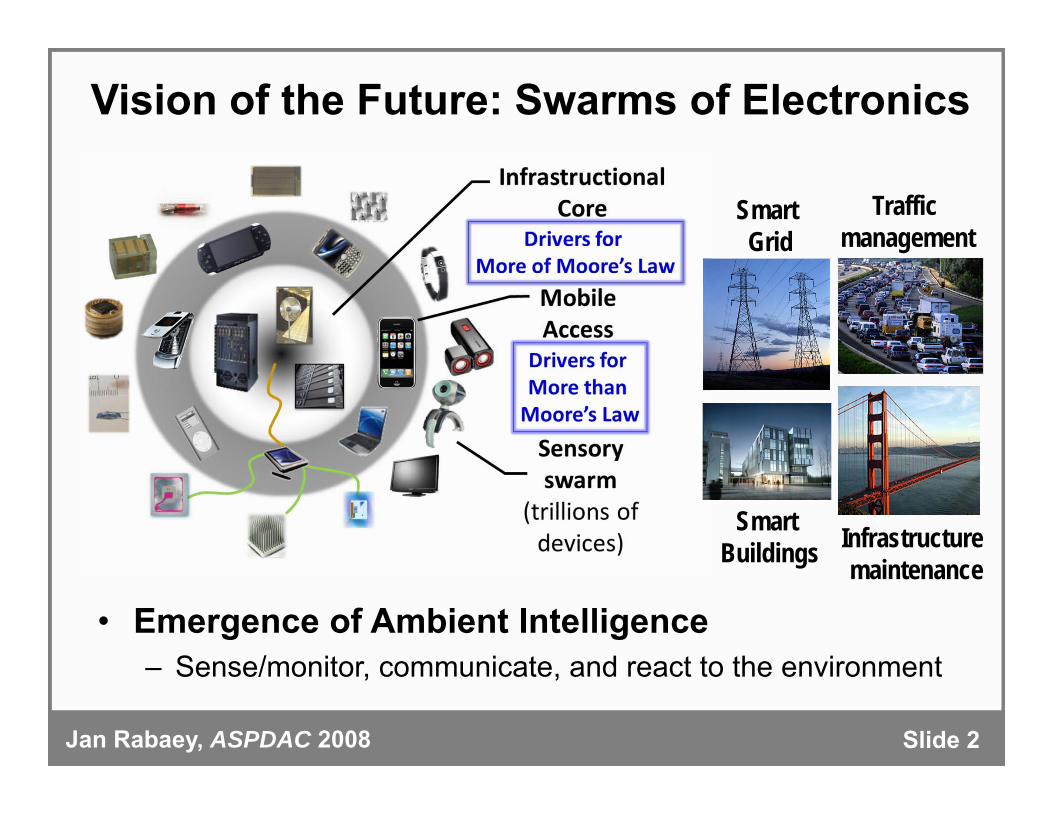
• Emergence of Ambient Intelligence– Sense/monitor, communicate, and react to the environment
Smart Grid
Traffic management
Smart Buildings Infrastructure
maintenance
Jan Rabaey, ASPDAC 2008
Vision of the Future: Swarms of Electronics
Slide 2

CMOS Voltage Scaling
• Scaling supply voltage (VDD) reduces circuit speed• Scaling threshold voltage (VT) increases leakage
Dra
in C
urre
nt I d
Gate Voltage Vg
scaling VT , VDD
S > 60mV/dec
Nor
mal
ized
Ener
gy/c
ycle
VDD(V)0.0
0.5
1.0
1.5
2.0
Etot
Edyn
Eleak
Slide 3

Why Relays?
• Zero OFF-state current (IOFF); abrupt switching– Turns on by electrostatic actuation when |VGS| ≥ VPI
– Turns off by spring restoring force when |VGS| ≤ VRL
GateSource Drain
OFF State Measured I-VCharacteristic
FElec
ON State
Slide 4
tgap tdimple

Relay Endurance
• Endurance increases exponentially with decreasing VDD, and linearly with decreasing CL
• Endurance is projected to exceed 1015 cycles @ 1V
H. Kam et al., IEDM 2010 Slide 5

4-Terminal (4-T) Relay for Digital Logic
• Voltage applied between the gate and body brings the channel into contact with the source and drain.‒ Folded-flexure design relieves residual stress.‒ Gate oxide layer insulates the channel from the gate.
Body
Drain
Source
Body
Gate
Channel
A
A’
Isometric View:
Drain Source
Gate
Body
GateOxide
substrate
IDS
insulator
AA’ cross-section: OFF state
AA’ cross-section: ON state
R. Nathanael et al., IEDM 2009 Slide 6

R. Nathanael et al., IEDM 2009; V. Pott et al., Proc. IEEE 2010
4-T Relay ID-VG Characteristics
• Zero IOFF and abrupt switching behavior observed• Hysteresis is due to pull-in mode operation
(tdimple > tgap/3) and contact surface adhesion.
Plan View SEM of 4-T Relay
20 μm1E-14
1E-12
1E-10
1E-08
1E-06
1E-04
1E-02
0 2 4 6 8 10I DS
(A)
VGS (V)
VD = 2VVS = 0V
VB = 0VVB = –9V
(a)
Slide 7

4 gate delays 1 mechanical delay
Digital IC Design with Relays
F. Chen et al., ICCAD 2008
• CMOS: delay is set by electrical time constant‒ Quadratic delay penalty for stacking devices Buffer & distribute logical/electrical effort over many stages
• Relays: delay is dominated by mechanical movement‒ Can stack ~100 devices before telec ≈ tmech
Implement relay logic as a single complex gate
Slide 8

Relay-Based VLSI Building Blocks
In collaboration with V. Stojanović (MIT) andD. Marković (UCLA)
F. Chen et al., ISSCC 2010 Slide 9

Relay Carry Generation Circuit
• Demonstrates propagate-generate-kill logic as a single complex gate
Slide 10F. Chen et al., ISSCC 2010

Energy-Delay Comparison with CMOS
M. Spencer et al., JSSC 2011; H. Fariborzi et al., ESSCIRC 2011
Ener
gy (f
J)Delay (ns)
Slide 11
• 90nm relay vs. CMOS adders and multipliers:>2-100× energy savings @ 3-100× higher delay

Outline• Introduction• Recent Progress
– Relay scaling– Multi-input/multi-output relay designs
• Current Challenges• Conclusion
Slide 12

Structural Layer Requirements• To reduce VPI, the effective spring constant (keff)
and actuation gap thickness (tgap) must be reduced.
where
Need to reduce the structural layer thickness (h)
∝ ∝
before release after release
1 2∆∝
z: tip deflection: radius of curvatureM: bending moment
Slide 13
• Strain gradient causes out-of-plane bending
Need very low strain gradient

Structural Film Development
• Thin TiN + poly-Si0.4Ge0.6bi-layer stack:– Tensile TiN compensates
strain gradient in Si0.4Ge0.6
• Interferometry topographshows low strain gradient of -7×10⁻⁴/µm(~10x improvement)
Movable Plate(Gate)
Source Drain
Body
5µm
Slide 14I-R. Chen et al., ECS Spring Meeting 2012

Gate
Drain 1 Drain 2
Body
Source 1 Source 2 0 100 2000
2
4
6
8
10
T [C]V
PI /
VR
L [V
]
VPIVRL
Slide 15
Single-Gate, Dual-Source/Drain Relay
I-R. Chen et al., ECS Spring Meeting 2012
Circuit Symbol
Measured I-VPlan-View SEM
Temperature Dependence:

VB_HIGH
VB_LOW
VOUTVINVOUT
VDD
GND
=1V
=13V
=‐12V
=0V
(INV) (BUF)
Slide 16
Single-Gate Relay Inverter/Buffer
R. Nathanael et al., VLSI-TSA 2012
1 0 1 1 000 1
BUF
INV
VOUT
VOUT
0
0.5
1
0 0.2 0.4
VIN(V)
0
0.5
1
0 0.2 0.4
VOUT(V)
Time (s)
(a)
(b)

Dual-Gate, Dual Source/Drain Relay
• Gate electrodes are interdigitatedto ensure that each gate has equal influence on the movable body
Bottom (Gate) Electrode Layout
Gate 1Gate 2
Drain 1 Drain 2
Body
Source 1 Source 2
Slide 17R. Nathanael et al., VLSI-TSA 2012
Circuit Symbol

0
4
8
12
16
20
Input [V IN1, V IN2]
VPI, V
RL (V
)
VPI VRL
[0, 1] [1, 0] [1, 1]
VDS=1.5V, VB=0V
Measured VPI and VRL of a Dual-Gate Relay
• “1”≡VG
• Each gate has equal influence
• Depending on VB, relay can be actuated using one or two gate electrodes
Gate 1
Gate 2
Slide 18R. Nathanael et al., VLSI-TSA 2012
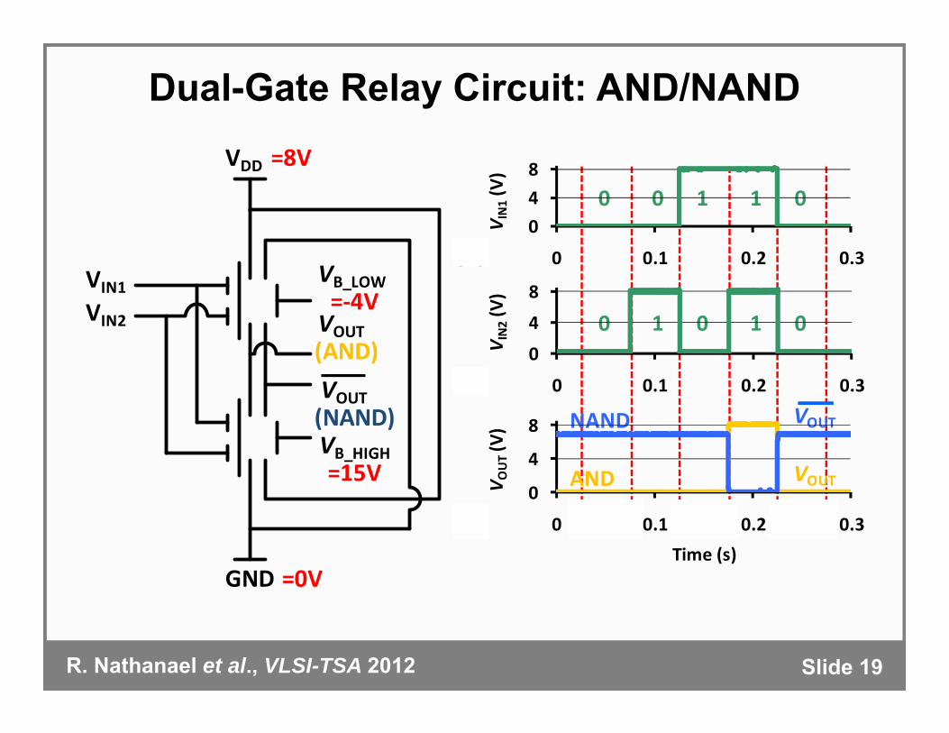
VIN1
GND
VIN2
VOUT
VOUT
VDD
VB_HIGH
VB_LOW
=8V
=0V
=15V
=‐4V
(AND)
(NAND)
(a)
(b)
(c)
0 0 1 1
0 1 0 1
0
0
NAND
AND
VOUT
VOUT
0
4
8
0 0.1 0.2 0.3
V IN2(V)
048
0 0.1 0.2 0.3
V IN1(V)
0
4
8
0 0.1 0.2 0.3V O
UT(V)
Time (s)
Slide 19
Dual-Gate Relay Circuit: AND/NAND
R. Nathanael et al., VLSI-TSA 2012
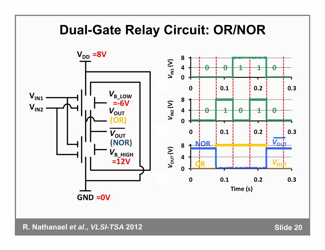
VIN1
GND
VIN2
VOUT
VOUT
VDD
VB_HIGH
VB_LOW
=8V
=0V
=12V
=‐6V
(OR)
(NOR)
(a)
(b)
(c)
0 0 1 1
0 1 0 1
0
00
4
8
0 0.1 0.2 0.3
V IN2(V)
048
0 0.1 0.2 0.3
V IN1(V)
NOR
OR
VOUT
VOUT0
4
8
0 0.1 0.2 0.3V O
UT(V)
Time (s)
Slide 20
Dual-Gate Relay Circuit: OR/NOR
R. Nathanael et al., VLSI-TSA 2012

Outline• Introduction• Recent Progress• Current Challenges
– Contact resistance– Surface adhesion
• Conclusion
Slide 21

Tungsten Contact Resistance Evolution
0
2
4
6
8
10
1.E+04 1.E+05 1.E+06 1.E+07 1.E+08 1.E+09
1 kHz5 kHz25 kHz
RO
N[kΩ
]
Number of Switching Cycles
Current
Surface oxide layers result in increased RON
Contacting surfaces oxidize when the relay is turned off
Joule heating occurs when the relay is on
Slide 22Y. Chen et al., IEEE/ASME J-MEMS 2012

Stiction: The Ultimate Relay Scaling Limiter • Hysteresis voltage (VPI-VRL) scales with VPI:
• Adhesive force reduces with contacting region area:
ignoring surface adhesion force
Extracted from measured VPI,VRL
0.04 um2
(W)
(W)
Slide 23J. Yaung et al., to be published
XSEM of Contact Dimple

Outline• Introduction• Recent Progress• Current Challenges• Conclusion
Slide 24

Conclusion• Relays have zero IOFF and can incorporate multiple
input/output electrodes potentially can achieve lower energy per operation
and greater functionality per device than CMOS for digital logic applications.
• Practical challenges remain to be solved: – Contact surface oxidation– Minimization of adhesion force within RON limits– Development of ultra-thin structural films with very
low strain gradient
Slide 25

Acknowledgments• Collaborators:
– Fred Chen, Hossein Fariborzi, Prof. Vladimir Stojanović (MIT)– Chengcheng Wang, Kevin Dwan, Prof. Dejan Marković (UCLA)
• Funding sources:– DARPA/MTO NEMS Program– SRC/DARPA Focus Center Research Program– NSF Center for Energy Efficient Electronics Science (E3S) – NSF Center of Integrated Nanomechanical Systems (COINS)– Berkeley Wireless Research Center
• Device fabrication support:– UC Berkeley Marvell Nanofabrication Laboratory– SVTC Technologies & SPTS Technologies
Slide 26