recommendations for board assembly of infineon ball grid
TRANSCRIPT

Additional Information Please read the Important Notice and Warnings at the end of this document Revision 4.0
www.infineon.com page 1 of 18 2020-11-09
Recommendations for Board Assembly of
Infineon Ball Grid Array Packages
Additional Information 2 of 18 Revision 4.0
2020-11-09
Recommendations for Board Assembly of Infineon Ball Grid Array
Packages Table of Contents
Table of Contents
Table of Contents ........................................................................................................................... 2
Acronyms and Abbreveations ........................................................................................................... 3
1 Package Description ............................................................................................................... 4
1.1 BGA Package Type ................................................................................................................................... 4 1.3 Package Features and General Handling Guidelines ............................................................................. 5
2 Printed Circuit Board .............................................................................................................. 7 2.1 Routing .................................................................................................................................................... 7
2.2 Pad Design ............................................................................................................................................... 7
3 PCB Assembly ........................................................................................................................ 9
3.1 Solder Paste Stencil ................................................................................................................................ 9
3.2 Solder Paste ............................................................................................................................................. 9 3.3 Component Placement ........................................................................................................................... 9
3.4 Reflow Soldering ................................................................................................................................... 10
4 Cleaning ............................................................................................................................... 11
5 Underfill ............................................................................................................................... 12
6 Inspection ............................................................................................................................ 13
6.1 Optical Solder Joint Inspection ............................................................................................................ 13 6.2 X-Ray Solder Joint Inspection ............................................................................................................... 13
7 Rework ................................................................................................................................ 15
8 References ........................................................................................................................... 16
Revision History ............................................................................................................................ 17
Additional Information 3 of 18 Revision 4.0
2020-11-09
Recommendations for Board Assembly of Infineon Ball Grid Array
Packages Acronyms and Abbreveations
Acronyms and Abbreveations
AOI ………………………………………… Automated Optical Inspection
AXI ………………………………………… Automated X-ray Inspection
BGA ………………………………………… Ball Grid Array
ESD ………………………………………… Electrostatic Discharge
IC ………………………………………… Integrated Circuit
IO ………………………………………… Input/Output
LFBGA ………………………………………… Low-profile Fine-pitch Ball Grid Array
NSMD ………………………………………… Non-Solder Mask Defined
PG ………………………………………… Plastic Green
PCB ………………………………………… Printed Circuit Board
SAC ………………………………………… Tin Silver Copper (SnAgCu)
SMD ………………………………………… Solder Mask Defined
SMD ………………………………………… Surface-Mount Device
SMT ………………………………………… Surface-Mount Technology
WLB ………………………………………… Wafer-Level Ball Grid Array
WLP ………………………………………… Wafer-Level Package
Additional Information 4 of 18 Revision 4.0
2020-11-09
Recommendations for Board Assembly of Infineon Ball Grid Array
Packages Package Description
1 Package Description
This document provides information about the board assembly of Ball Grid Array (BGA) packages with a multi-
layer glass woven epoxy substrate. The terminations consist of lead-free solder balls that allow for assembly by Surface Mount Technology (SMT). This document does not discuss Wafer-Level Ball Grid Array (WLB) packages or comparable Wafer-Level Packages (WLP). These package families are described in a separate document.
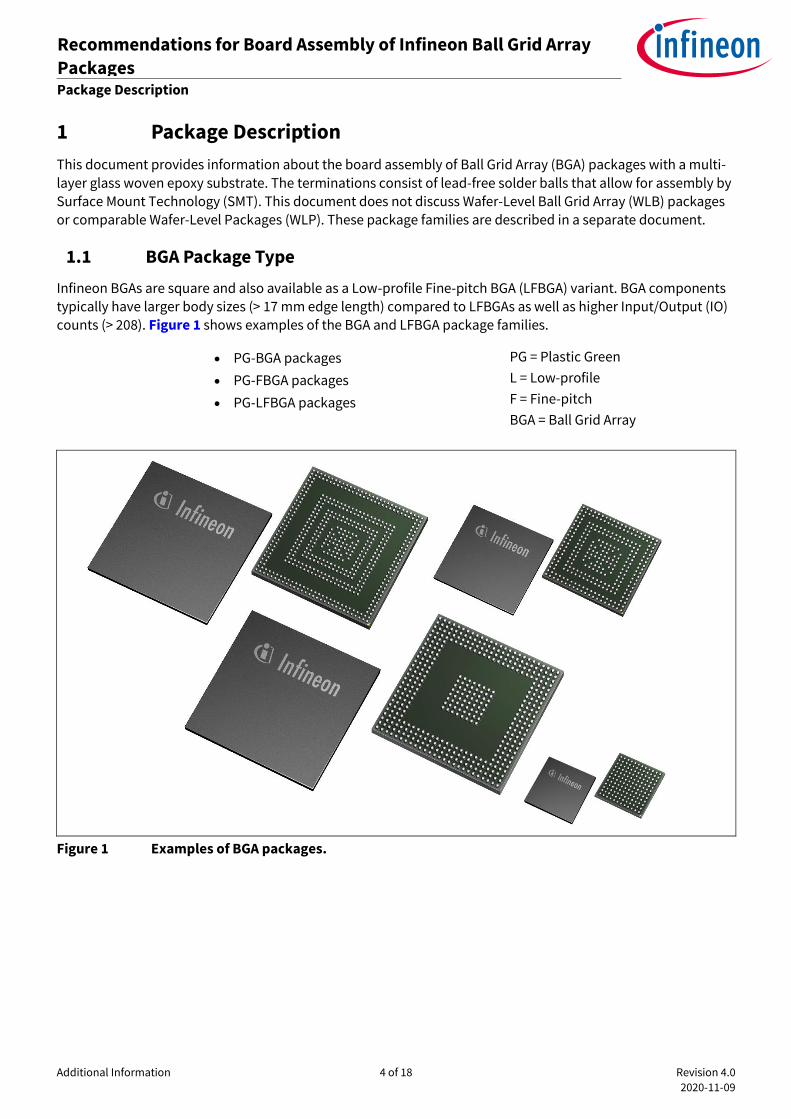
1.1 BGA Package Type
Infineon BGAs are square and also available as a Low-profile Fine-pitch BGA (LFBGA) variant. BGA components typically have larger body sizes (> 17 mm edge length) compared to LFBGAs as well as higher Input/Output (IO) counts (> 208). Figure 1 shows examples of the BGA and LFBGA package families.
PG-BGA packages
PG-FBGA packages
PG-LFBGA packages
PG = Plastic Green
L = Low-profile
F = Fine-pitch
BGA = Ball Grid Array
Figure 1 Examples of BGA packages.
Additional Information 5 of 18 Revision 4.0
2020-11-09
Recommendations for Board Assembly of Infineon Ball Grid Array
Packages Package Description
1.3 Package Features and General Handling Guidelines
General Handling Guidelines
Semiconductor devices are sensitive to excessive electrostatic discharge (ESD), moisture, mechanical handling, and contamination. Therefore, they require specific precautionary measures to ensure that they are not
damaged during transport, storage, handling, and processing.
For further information about component handling, please refer to the General Recommendations for Board Assembly of Infineon Packages document that is available on the Infineon web page [1]. Please also feel free to
contact your local sales, application, or quality engineer.
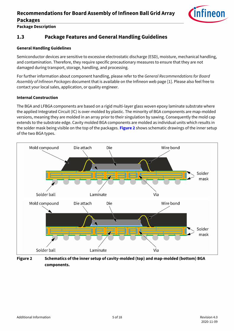
Internal Construction
The BGA and LFBGA components are based on a rigid multi-layer glass woven epoxy laminate substrate where the applied Integrated Circuit (IC) is over-molded by plastic. The minority of BGA components are map-molded versions, meaning they are molded in an array prior to their singulation by sawing. Consequently the mold cap
extends to the substrate edge. Cavity molded BGA components are molded as individual units which results in the solder mask being visible on the top of the packages. Figure 2 shows schematic drawings of the inner setup
of the two BGA types.
Figure 2 Schematics of the inner setup of cavity-molded (top) and map-molded (bottom) BGA
components.
Additional Information 6 of 18 Revision 4.0
2020-11-09
Recommendations for Board Assembly of Infineon Ball Grid Array
Packages Package Description
Termination Design
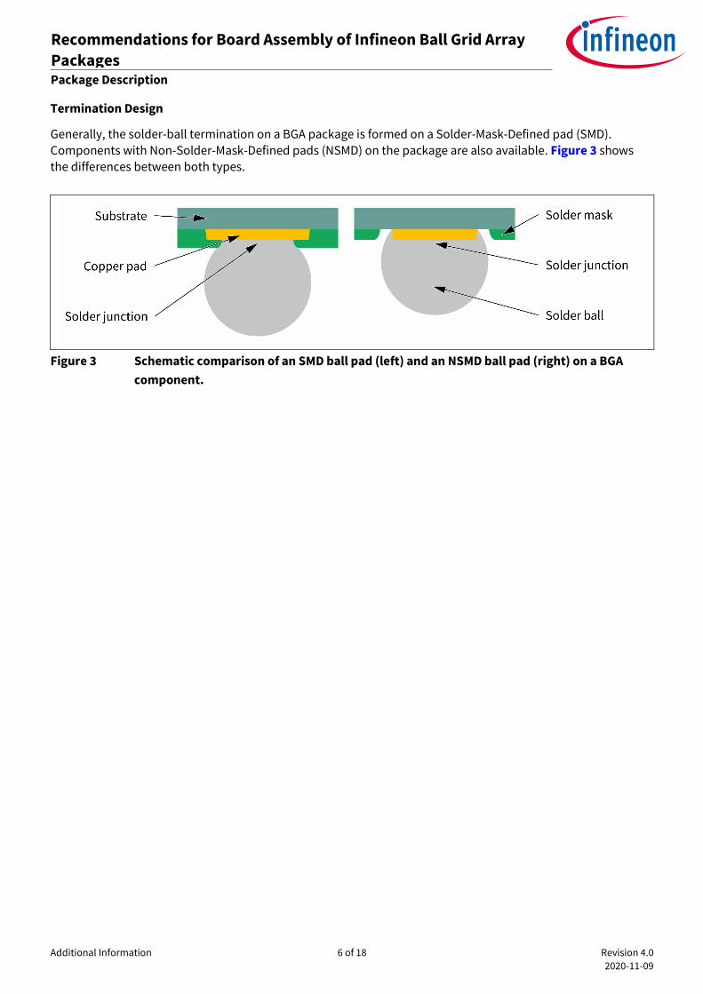
Generally, the solder-ball termination on a BGA package is formed on a Solder-Mask-Defined pad (SMD). Components with Non-Solder-Mask-Defined pads (NSMD) on the package are also available. Figure 3 shows the differences between both types.
Figure 3 Schematic comparison of an SMD ball pad (left) and an NSMD ball pad (right) on a BGA
component.
Additional Information 7 of 18 Revision 4.0
2020-11-09
Recommendations for Board Assembly of Infineon Ball Grid Array
Packages Printed Circuit Board
2 Printed Circuit Board
2.1 Routing
The main difference between components with solder balls such as BGA and conventional SMD such as
leadframe-based components is the array configuration of solder spheres on the package. This implies different concepts for routing the signal, power, and ground pins on the Printed Circuit Board (PCB). Typically
fine-line PCBs with conductor width/spacing of 100 µm are necessary for routing. The specifics of the PCB design to be used strongly depend on the board technology (conventional technology with drilled vias, build-up technology with microvias), the conductor width/spacing, number of metal layers, and electrical
restrictions.
The PCB design and construction are key factors for achieving highly reliable solder joints. BGA packages should not be placed opposite one another on the PCB (if double sided mounting is used), because this stiffens
the assembly and results in earlier solder-joint fatigue compared to a design where the components are offset. Furthermore, the board stiffness itself has a significant effect on the reliability (temperature cycling) of the
solder-joint interconnect if the system is used in critical temperature-cycling conditions. The lower bending stiffness of thinner boards (e.g. 1.0 mm) improves solder-joint reliability (temperature cycling) compared to
thick boards (e.g. 2.35 mm).
2.2 Pad Design
The quality and reliability of interconnect solder joints to the board are affected by:
Pad type (Solder Mask Defined, SMD or Non-Solder Mask Defined, NSMD)
Specific pad dimensions
Pad finish (also called metallization or final finish)
Via layout and technology
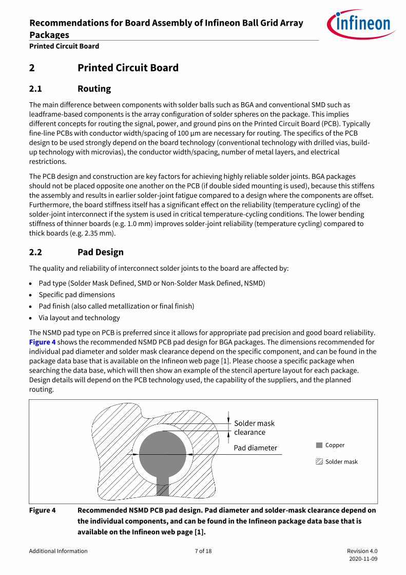
The NSMD pad type on PCB is preferred since it allows for appropriate pad precision and good board reliability. Figure 4 shows the recommended NSMD PCB pad design for BGA packages. The dimensions recommended for individual pad diameter and solder mask clearance depend on the specific component, and can be found in the
package data base that is available on the Infineon web page [1]. Please choose a specific package when searching the data base, which will then show an example of the stencil aperture layout for each package.
Design details will depend on the PCB technology used, the capability of the suppliers, and the planned routing.
Figure 4 Recommended NSMD PCB pad design. Pad diameter and solder-mask clearance depend on
the individual components, and can be found in the Infineon package data base that is
available on the Infineon web page [1].
Additional Information 8 of 18 Revision 4.0
2020-11-09
Recommendations for Board Assembly of Infineon Ball Grid Array
Packages Printed Circuit Board
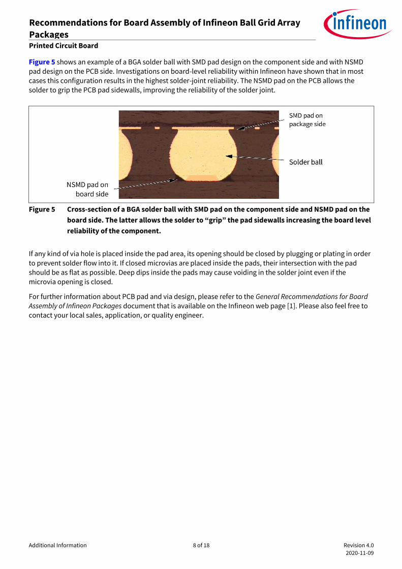
Figure 5 shows an example of a BGA solder ball with SMD pad design on the component side and with NSMD pad design on the PCB side. Investigations on board-level reliability within Infineon have shown that in most
cases this configuration results in the highest solder-joint reliability. The NSMD pad on the PCB allows the solder to grip the PCB pad sidewalls, improving the reliability of the solder joint.
Figure 5 Cross-section of a BGA solder ball with SMD pad on the component side and NSMD pad on the
board side. The latter allows the solder to “grip” the pad sidewalls increasing the board level
reliability of the component.
If any kind of via hole is placed inside the pad area, its opening should be closed by plugging or plating in order
to prevent solder flow into it. If closed microvias are placed inside the pads, their intersection with the pad should be as flat as possible. Deep dips inside the pads may cause voiding in the solder joint even if the
microvia opening is closed.
For further information about PCB pad and via design, please refer to the General Recommendations for Board
Assembly of Infineon Packages document that is available on the Infineon web page [1]. Please also feel free to contact your local sales, application, or quality engineer.
Additional Information 9 of 18 Revision 4.0
2020-11-09
Recommendations for Board Assembly of Infineon Ball Grid Array
Packages PCB Assembly
3 PCB Assembly
3.1 Solder Paste Stencil
In SMT, the solder paste is applied onto the PCB metal pads by stencil printing. The volume of the printed
solder paste is determined by the stencil aperture and the stencil thickness.
The stencil aperture for BGA packages should be circular. The stencil thickness can vary between 100 and 150 μm depending on aperture area ratio, the stencil material, and the aperture diameter. Specific stencil
aperture recommendations can be found in the package data base that is available on the Infineon web page [1]. Please choose a specific package when searching the data base, which will then show an example of the stencil aperture layout for each package.
To ensure a uniform and sufficient solder paste transfer to the PCB, laser-cut stencils (mostly made from stainless steel) or electroformed stencils (nickel) are preferred. For individual design adaptations to use the optimum amount of solder, the stencil thickness, the PCB pad finish, quality and solder masking, the via layout,
and the solder paste type should be considered. In every case, application-specific experiments are recommended.
For further information about solder stencil design, please refer to the General Recommendations for Board Assembly of Infineon Packages document that is available on the Infineon web page [1]. Please also feel free to
contact your local sales, application, or quality engineer.
3.2 Solder Paste
Pb-free solder pastes typically contain some type of SnAgCu alloy (SAC solder with typically 1-4% Ag and <1%
Cu). The most common alloy is SAC305 (3.0% Ag and 0.5% Cu). The average alloy particle size must be suitable
for printing the solder stencil aperture dimensions. Using Type 3 or Type 4 paste is recommended for the assembly of BGA components, depending on the specific stencil transfer.
The solder alloy particles are dispersed in a blend of liquid flux and chemical additives (approx. 50% by volume
or 10% by weight), forming a creamy paste. The flux and chemical solvents have various functions such as
adjusting the viscosity of the paste for stencil printing or removing contamination and oxides from the surface.
The solder paste solvents have to evaporate during reflow soldering, while residues of the flux will remain on
the solder joint. The capacity of the flux additive for removing oxides is given by its activation level, which also affects the potential need for removing the flux residuals after the assembly. For area-array packages such as
BGA, in which the solder joint is formed mainly on the bottom side, a “no-clean” paste is recommended to avoid subsequent cleaning underneath the package. The small gaps make cleaning highly difficult if not
impossible. Certain precautions have to be taken if any kinds of flux residues remain on the board prior to any
kind of coating.
Generally, solder paste is sensitive to ageing, temperature, and humidity. Please follow the handling recommendations of the paste manufacturer.
3.3 Component Placement
Although the self-alignment effect due to the surface tension of the liquid solder will support the formation of reliable solder joints, the components have to be placed accurately depending on their geometry. Positioning the packages manually is not recommended, especially for packages with small terminations and pitch. An automated pick-and-place machine is recommended to obtain reliable solder joints.
Component placement accuracies of +/-50 µm and less are obtained with modern automatic component placement machines using vision systems. With these systems, both the PCB and the components are optically
Additional Information 10 of 18 Revision 4.0
2020-11-09
Recommendations for Board Assembly of Infineon Ball Grid Array
Packages PCB Assembly
measured and the components are placed on the PCB at their programmed positions. The fiducials on the PCB are located either on the edge of the PCB for the entire PCB, or at additional individual mounting positions
(local fiducials). These fiducials are detected by a vision system immediately prior to the mounting process. Most such vision systems provide special lighting and algorithms for area array packages. For BGA components
it is recommended to use the ball recognition instead of the component outline recognition for centering. This approach eliminates potential tolerances between the solder ball and the package.
When placing BGA packages, the placement force should be sufficiently high, while avoiding excessive placement force that can squeeze the solder paste out of its intended location and cause solder joint shorts.
For further information about component placement, please refer to the General Recommendations for Board Assembly of Infineon Packages document that is available on the Infineon web page [1]. Please also feel free to contact your local sales, application, or quality engineer.
3.4 Reflow Soldering
For printed PCB assembly of the BGA components, the widely used method of reflow soldering in a forced convection oven is recommended. Soldering in a nitrogen atmosphere can generally improve the solder joint quality but is not necessary to create a reliable joint.
The soldering profile should be in accordance with the recommendations of the solder paste manufacturer to achieve optimal solder-joint quality. The position and the surrounding of the component on the PCB, as well as
the PCB thickness, can influence the solder joint temperature significantly.
Minimum Reflow Conditions
The lower temperatures and durations of an optimal reflow profile shall stay above those of the wettability test
profile of a solderability qualification. The solderability of the terminations of Infineon components is tested
according to the standards IEC-60068-2-58 and J-STD-002 [2][3].
Maximum Reflow Conditions and Cycles
Components that are Moisture-Sensitivity Level (MSL) classified by Infineon have been tested by three reflow
runs in accordance with the J-STD-020 standard, including a double-sided reflow and one rework cycle. The maximum temperatures must not be exceeded during board assembly. Please refer to the product barcode
label on the packing material that states this maximum reflow temperature according to the J-STD-020 [4] standard as well as the MSL according to the J-STD-033 standard [5].
BGA packages are generally suited for double-sided PCB mounting. That means that both sides of the PCB are fitted and reflowed one after another. As a consequence, the side that was initially assembled experiences two reflow cycles. During the second cycle, the components are hanging upside-down. Therefore, during the peak
zone of the reflow profile (where the solder is liquid), the components are only held by wetting forces of the
molten solder. Gravity acting in the opposite direction will elongate the solder joints, unlike joints on the top side, where gravity forces the components nearer to the PCB surface. This shape will be frozen during cooling and therefore will result in a higher stand-off on the bottom side after the reflow process. Any mechanical
impacts on components that are soldered upside down should be avoided.
BGA components have a natural tendency for warpage due to its layered construction. During package
development projects the warpage is addressed by specific investigations in order to minimize a potential
impact on the solder joint formation.
For further information about reflow soldering, please refer to the General Recommendations for Board Assembly of Infineon Packages document that is available on the Infineon web page [1]. Please also feel free to contact your local sales, application, or quality engineer.
Additional Information 11 of 18 Revision 4.0
2020-11-09
Recommendations for Board Assembly of Infineon Ball Grid Array
Packages Cleaning
4 Cleaning
After the soldering process, some flux residues will remain on the board, especially near the solder joints.
Generally, cleaning beneath a component with bottom-only terminations is difficult due to the small gap between the component body and the PCB. Therefore, a “no-clean” flux is recommended whose residues usually do not have to be removed after the soldering process.
In case the solder joints have to be cleaned, the cleaning method (e.g. ultrasonic, spray, or vapor cleaning) and cleaning solution have to be selected while taking into account the type of package, the flux used in the solder paste (rosin/resin-based, water-soluble, etc.) as well as the environmental and safety aspects. Even small
residues of the cleaning solution should be removed or dried out very thoroughly. For recommended cleaning solutions, please contact the solder paste or flux manufacturer.
Additional Information 12 of 18 Revision 4.0
2020-11-09
Recommendations for Board Assembly of Infineon Ball Grid Array
Packages Underfill
5 Underfill
An underfill process may improve board-level reliability, but this depends highly on the underfill material
properties, the individual mounting situation of the package, and the general application requirements of the entire system. Generally, BGA components are known for their high board-level reliability due to their inherent package construction.
In case of questions on underfilling BGA components, please contact your local sales, application, or quality engineer.
Additional Information 13 of 18 Revision 4.0
2020-11-09
Recommendations for Board Assembly of Infineon Ball Grid Array
Packages Inspection
6 Inspection
6.1 Optical Solder Joint Inspection
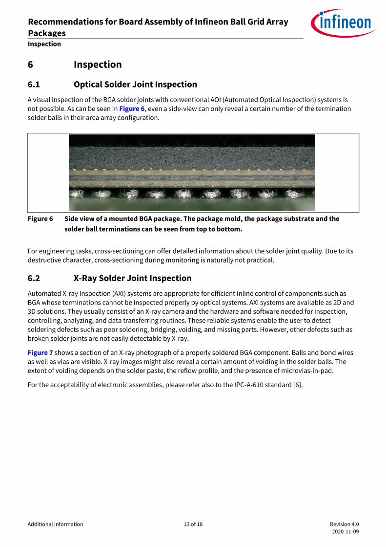
A visual inspection of the BGA solder joints with conventional AOI (Automated Optical Inspection) systems is
not possible. As can be seen in Figure 6, even a side-view can only reveal a certain number of the termination solder balls in their area array configuration.
Figure 6 Side view of a mounted BGA package. The package mold, the package substrate and the
solder ball terminations can be seen from top to bottom.
For engineering tasks, cross-sectioning can offer detailed information about the solder joint quality. Due to its
destructive character, cross-sectioning during monitoring is naturally not practical.
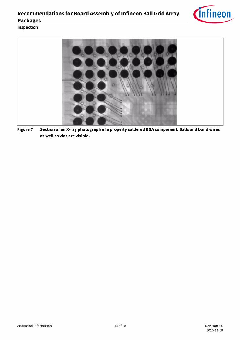
6.2 X-Ray Solder Joint Inspection
Automated X-ray Inspection (AXI) systems are appropriate for efficient inline control of components such as BGA whose terminations cannot be inspected properly by optical systems. AXI systems are available as 2D and 3D solutions. They usually consist of an X-ray camera and the hardware and software needed for inspection,
controlling, analyzing, and data transferring routines. These reliable systems enable the user to detect
soldering defects such as poor soldering, bridging, voiding, and missing parts. However, other defects such as broken solder joints are not easily detectable by X-ray.
Figure 7 shows a section of an X-ray photograph of a properly soldered BGA component. Balls and bond wires as well as vias are visible. X-ray images might also reveal a certain amount of voiding in the solder balls. The
extent of voiding depends on the solder paste, the reflow profile, and the presence of microvias-in-pad.
For the acceptability of electronic assemblies, please refer also to the IPC-A-610 standard [6].
Additional Information 14 of 18 Revision 4.0
2020-11-09
Recommendations for Board Assembly of Infineon Ball Grid Array
Packages Inspection
Figure 7 Section of an X-ray photograph of a properly soldered BGA component. Balls and bond wires
as well as vias are visible.
Additional Information 15 of 18 Revision 4.0
2020-11-09
Recommendations for Board Assembly of Infineon Ball Grid Array
Packages Rework
7 Rework
Single solder joint repair of bottom-only terminated packages is highly difficult, if not impossible, and is
therefore generally not recommended. Furthermore, the reuse of de-soldered components is not recommended. The de-soldered components should be replaced by new ones.
A rework process is commonly done on special rework equipment. There are various systems available that meet the requirements for reworking SMD packages. All handling guidelines discussed in this document have to be respected. Special focus should be on the following items:
Due to the decreased automation level given by the general rework approach, even higher care compared to standard assembly must be taken. Tools that do not damage the component mechanically have to be chosen. Mechanical forces that do not necessarily cause visible external damage can still cause internal
damage that reduces the component’s reliability. A proper handling system with vacuum nozzle may be the gentlest process and is therefore recommended. However, the impact of rework tools has to be assessed properly. In general, more manual handling increases the effort for documentation, training, and monitoring of the rework process(es).
During rework, special care must be taken concerning the proper moisture level of the component according to the J-STD-033. Drying the PCB and the component prior to rework might be necessary. A proper drying procedure for SMD packages is described in the international J-STD-033 standard [5].
Please also refer to the recommendations of your PCB manufacturer and take all specific needs of components, PCB, and other materials into account.
Whatever heating system is used (hot air, infrared, hot plate, etc.), the applied temperature profile at the component must never exceed the maximum temperature according to the J-STD-020 standard. Depending on the specific heating profile used during rework, components adjacent to the mounting
location might also experience a further “reflow run” in terms of the J-STD-020 standard [4]. Internal
investigations have shown that the temperature profile must be recorded.
If a device is suspected to be defective and a failure analysis is planned, Infineon usually expects customers to desolder the component prior to return to Infineon. The component shall be returned in a proper condition
according to the original package outlines.
In some special cases such as solder joint inspection Infineon may request that the PCB or part of the PCB with the component still attached should be sent to Infineon.
Note: Before returning a device for failure analysis at Infineon, please clarify the return condition of the suspected component (ie onboard or desoldered) with the Infineon Application Engineer or
Customer Quality Manager who supports your company.
For further information about component rework on PCB, please refer to the General Recommendations for
Board Assembly of Infineon Packages document that is available on the Infineon web page [1]. Please also feel free to contact your local sales, application, or quality engineer.
Additional Information 16 of 18 Revision 4.0
2020-11-09
Recommendations for Board Assembly of Infineon Ball Grid Array
Packages References
8 References
[1] Infineon Technologies: Packages. www.infineon.com\packages.
[2] International Electrotechnical Commission: IEC 60068-2-58. Environmental testing - Part 2-58: Tests - Test Td: Test methods for solderability, resistance to dissolution of metallization and to soldering heat of
surface mounting devices (SMD).
[3] Electronic Components Industry Association, Assembly and Joining Processes and JEDEC Solid State Technology Association Committee: EIA/IPC/JEDEC J-STD-002. Solderability Tests for Component Leads,
Terminations, Lugs, Terminals and Wires.
[4] JEDEC Solid State Technology Association: IPC/JEDEC J-STD-020. Moisture/Reflow Sensitivity
Classification for Nonhermetic Surface Mount Devices.
[5] JEDEC Solid State Technology Association: IPC/JEDEC J-STD-033. Handling, Packing, Shipping and Use of
Moisture/Reflow Sensitive Surface Mount Devices.
[6] Association Connecting Electronics Industries: IPC-A-610. Acceptability of Electronic Assemblies.

Additional Information 17 of 18 Revision 4.0
2020-11-09
Recommendations for Board Assembly of Infineon Ball Grid Array
Packages Revision History
Revision History
Page or reference Major changes since the last revision
Section 7 “Rework” Update of sample conditions in case of return.
Section 5 “Underfill” Transfer of content from former section 3.5.
Entire document Editorial review.

Trademarks All referenced product or service names and trademarks are the property of their respective owners.
Edition 2020-11-09
Published by
Infineon Technologies AG
81726 Munich, Germany
© 2020 Infineon Technologies AG.
All Rights Reserved.
Do you have a question about this
document?
Email: [email protected]
Document reference
IMPORTANT NOTICE The information contained in this application note is given as a hint for the implementation of the product only and shall in no event be regarded as a description or warranty of a certain functionality, condition or quality of the product. Before implementation of the product, the recipient of this application note must verify any function and other technical information given herein in the real application. Infineon Technologies hereby disclaims any and all warranties and liabilities of any kind (including without limitation warranties of non-infringement of intellectual property rights of any third party) with respect to any and all information given in this application note. The data contained in this document is exclusively intended for technically trained staff. It is the responsibility of customer’s technical departments to evaluate the suitability of the product for the intended application and the completeness of the product information given in this document with respect to such application.
For further information on the product, technology, delivery terms and conditions and prices please contact your nearest Infineon Technologies office (www.infineon.com).
WARNINGS Due to technical requirements products may contain dangerous substances. For information on the types in question please contact your nearest Infineon Technologies office. Except as otherwise explicitly approved by Infineon Technologies in a written document signed by authorized representatives of Infineon Technologies, Infineon Technologies’ products may not be used in any applications where a failure of the product or any consequences of the use thereof can reasonably be expected to result in personal injury.