reconfigurable wideband circularly polarized stacked ... · u.s. government work not protected by...
TRANSCRIPT
U.S. Government work not protected by U.S. copyright
Reconfigurable Wideband Circularly Polarized Stacked Square Patch Antenna for Cognitive Radios
Miguel A. Barbosa Kortright University of Puerto Rico, Mayagüez Campus
Mayagüez, PR 00680 [email protected]
Seth W. Waldstein University of Cincinnati, Main Campus
Cincinnati, OH 45221-0063 [email protected]
Rainee N. Simons
NASA Glenn Research Center Cleveland, OH 44135
Abstract—An almost square patch, a square patch and a stacked square patch with corner truncation for circular polarization (CP) are researched and developed at X-band for cognitive radios. Experimental results indicate, first, that the impedance bandwidth of a CP almost square patch fed from the edge by a 50 ohm line is 1.70% and second, that of a CP square patch fed from the ground plane side by a surface launch connector is 1.87%. Third, the impedance bandwidth of a CP stacked square patch fed by a surface launch connector is 2.22%. The measured center frequency for the CP square patch fed by a surface launch connector without and with an identical stacked patch is 8.45 and 8.1017 GHz, respectively. By stacking a patch, separated by a fixed air gap of 0.254 mm, the center frequency is observed to shift by as much as 348.3 MHz. The shift in center frequency, brought about by the reconfiguring of the physical layer antenna, can be exploited in a cognitive system since it expands the usable frequency spectrum for software reconfiguration in the presence of interference. In addition, varying the fixed air gap in the stacked antenna geometry by increments of 0.254 mm further expands the usable frequency spectrum.
Keywords—Microstrip; circular polarization; stacked patch antenna; cognitive; reconfigurable; X-band; surface launch excitation; cognitive radio; wideband antenna
I. INTRODUCTION
One of the greatest design challenges for cognitive radio antennas is creating wideband elements. Software defined radio (SDR) is seen as an enabling technology for cognitive radio, which offers much promise to increase spectrum usage efficiencies to users in a wide variety of applications, including space communications [1]. In the context of space communications, NASA’s Near Earth Network (NEN) is interested in the X-Band frequencies (8.0 to 8.5 GHz) to establish space-to-Earth downlinks for science spacecraft using cognitive radios. The use of this frequency band can be achieved through the reconfigurable nature of cognitive radios. Reconfiguration in cognitive radios is achieved through the use of software modules to adapt the radio’s internal states to statistical variations in the incoming RF stimuli [2] and [3]. The
physical layer of the cognitive radio (antennas, conversion modules, etc.) is not often associated with the reconfigurable capabilities of the cognitive radio. In this paper, the design of wideband circularly polarized (CP) patch antennas for frequency reconfiguration in the physical layer of cognitive radios are studied and reported at X-Band frequencies.
Due to their lightweight, low cost, and ease of fabrication, patch antennas are attractive for wireless communications. The drawback for these antennas is their narrow bandwidth [4]. Two designs were researched and fabricated to improve bandwidth and demonstrate frequency reconfiguration at the physical level for cognitive devices: (1) A microstrip almost square patch antenna with corner truncation for CP, fed through the edge with a 50 ohm microstrip line; (2) A microstrip square patch antenna with corner truncation for CP, fed from the ground plane side with a surface launch connector. These designs were studied as both standalone and stacked geometries. A stacked square patch with corners truncated for CP, fed from the edge by a 50 ohm line and having an impedance bandwidth of 1.3 GHz (11.2 to 12.5 GHz) has been demonstrated in [5]. However, this geometry offers considerable challenges in the realization of large arrays since it would require the antennas and feed networks to be in a planar configuration [6]. To address this issue, the microstrip square patch fed from the ground plane side with a surface launch connector was investigated in greater detail. This type of feeding arangement has several advantages: (1) It can be configured into a large planar array, (2) It allows for hybrid integration of phase-shifters and solid-state power amplifiers (SSPA) located either on an orthogonal substrate or on a multi-layer substrate, (3) It can be scaled to higher frequencies of interest to NASA missions.
Reconfiguration of the physical layer of the cognitive radio becomes feasable when a stacked antenna is added into the system. The stacked antenna element creates the potential of a mechanically tunable system, expanding the usable antenna net impedance bandwidth and operating frequencies for use in spectrum sensing and transmission. The mechanical tunning of the stacked antenna is achievable through the addition of an external mechanism, such as RF-MEMS circuitry.
https://ntrs.nasa.gov/search.jsp?R=20170006030 2018-09-07T03:06:25+00:00Z

U.S. Government work not protected by U.S. copyright
II. MICROSTRIP PATCH ANTENNA DESIGN AND SIMULATION
A. Standalone Antennas
The antennas were designed and simulated using CST Microwave Studios 2010 and its built in material library [7]. Roger’s Corporation’s RO3003 (εr = 3.0, h = 0.508 mm, g = 60 mm) substrate with half-ounce cooper cladding (t = 0.01778 mm) was considered for the antennas.
The lengths and widths (L1, W1, L2, and W2) and corner truncations (C1 and C2) for the antennas in Fig. 1 were calculated with equations from [8]. The Trust Region Algorithm was utilized in CST to optimize the antenna dimensions in order to get the best possible results for the design frequency of 8.4 GHz. The corner truncation makes CP possible. In Fig. 1, the corner truncations resulted in an antenna that is left hand circularly polarized (LHCP). Truncating the opposite two corners will result in an antenna that is right hand circularly polarized (RHCP). The dimension G represents the width of the 50 ohm transmission line that is used to feed the almost square patch antenna and is calculated using ADS’s Line Calc. The dimension D represents the final optimized position with respect to the center of the square patch antenna in which the surface launch connector pin is introduced from the ground plane side of the substrate. Table I summarizes the antenna dimensions.
(a) (b)
Fig. 1. Standalone antenna geometry. (a) Almost square patch with 50 ohms microstrip feed. (b) Square patch excited from the ground plane side by a surface launch connector.
TABLE I. DIMENSIONS OF THE STANDALONE ANTENNAS (mm)
Dimensions L1 10.337 W1 10 C1 1.487 G 1.277 L2 9.856 W2 9.856 C2 0.873 D 2
There is not much information on the exact location of an efficient feed point for the surface launch type of excitation in the open literature for X-Band applications. It is reported in [9] that at 2.48 GHz a good feed point could be 55% towards the edge, from the center point of the antenna. A study reported in [10] indicated that the best input VSWR for a patch at 3.103 GHz was obtained with a feed point 64% towards the edge, from the center point of the antenna. Consequently, in the initial design the position of the feed point was placed between 45% and 55% towards the edge, from the center point of the antenna. The final CST optimized position represented a move of 40.4% towards the edge, from the center point of the antenna. The simulation took into consideration the surface launch connector pin radius and dielectric radius of 0.254 and 1.016 mm, respectively. The ground plane corresponding to the cross sectional area of the connector dielectric is removed in the simulation to match the fabricated geometry.
B. Stacked Antenna
The stacked square patch antenna geometry consists of an identical patch antenna without a ground plane stacked on top of a driven patch antenna, as illustrated in Fig. 2. The driven patch and the stacked patch have identical substrate properties. There is a fixed minimum air gap of 0.254 mm between the driven patch and stacked patch due to the solder bump that was created during the assembly process to hold the coaxial connector pin in place.
It is worth mentioning that by stacking a patch on an almost square patch with a 50 ohm feed would also impact the feed line propagation characteristics (Fig. 1(a)). This is because the over layed stacked dielectric substrate now appears as a superstrate for the feed line. Such an arrangement would necessitate reconfiguring the 50 ohm feed line and the patch antenna characteristics simultaneously, which would render the stacked antenna design far more complicated. Therefore, the stacked geometry was only pursued for the standalone square patch, fed from the ground plane side by a surface launch connector (Fig. 1(b)).
Fig. 2. Stacked square patch antenna geometry with identical driven and
stacked patches.

U.S. Government work not protected by U.S. copyright
C. Simulated Results – Center Frequency and Impedance Bandwidth
Figs. 3(a) and (b) shows the simulated S11 for the two standalone geometries (Fig. 1). The simulated results show that the center frequency (f0) for both standalone cases are similar and close to the design frequency of 8.4 GHz. The return loss magnitude at f0 for the square patch is better than the almost square patch by approximately 3 dB. In addition, the square patch had a better impedance bandwidth (BW) than the standalone almost square patch by 0.24%. Table II presents a summary of the information extracted from Figs. 3(a) and (b).
Fig. 3. Simulated and Experimental S11: (a) Almost square patch, (b) Square
patch, (c) Stacked square patch. Simulated VSWR: (d) All three cases.
Fig. 3(c) shows the simulated S11 for the stacked square patch antenna (Fig. 2). The simulated center frequency for the square patch excited by a surface launch connector without and with a stacked patch is 8.364 and 8.076 GHz, respectively. Thus by stacking a patch, separated by a fixed air gap of 0.254 mm, the center frequency is observed to shift by as much as 288 MHz (3.44%). In addition, the impedance bandwidth increases by 0.5%. It is worth noting that by increasing the air gap to 1.27 mm in increments of 0.254 mm, the center frequency of the stacked system moved closer to the center frequency of the stand alone system. The effects of the air gap is discussed in a further section. Table III summarizes the data extracted from Fig. 3(c). Fig. 3(d) shows the VSWR for all three cases and is observed to be under two, which is desireable.
TABLE II. SUMMARY OF CST SIMULATED S11 AND BANDWIDTH DATA FOR STANDALONE ALMOST SQUARE PATCH AND SQUARE PATCH ANTENNAS
f0 (GHz)
Return Loss (dB)
fL (GHz)
fH (GHz)
BW = fH - fL (MHz)
BW/f0
(%)
Standalone Almost Square Patch, Fed From Edge
8.356 13.460 8.2888 8.4203 131.5 1.57
Standalone Square Patch, Fed Through Back With Surface Launch Connector
8.364 16.375 8.2797 8.4314 151.7 1.81
TABLE III. SUMMARY OF CST SIMULATED S11 AND BANDWIDTH DATA FOR STACKED SQUARE PATCH ANTENNA FOR A FIXED AIR GAP OF 0.254 mm
f0 (GHz)
Return Loss (dB)
fL (GHz)
fH (GHz)
BW = fH - fL (MHz)
BW/f0 (%)
Stacked Square Patch, Fed Through Back With Surface Launch Connector
8.076 18.869 7.9755 8.1625 187 2.31
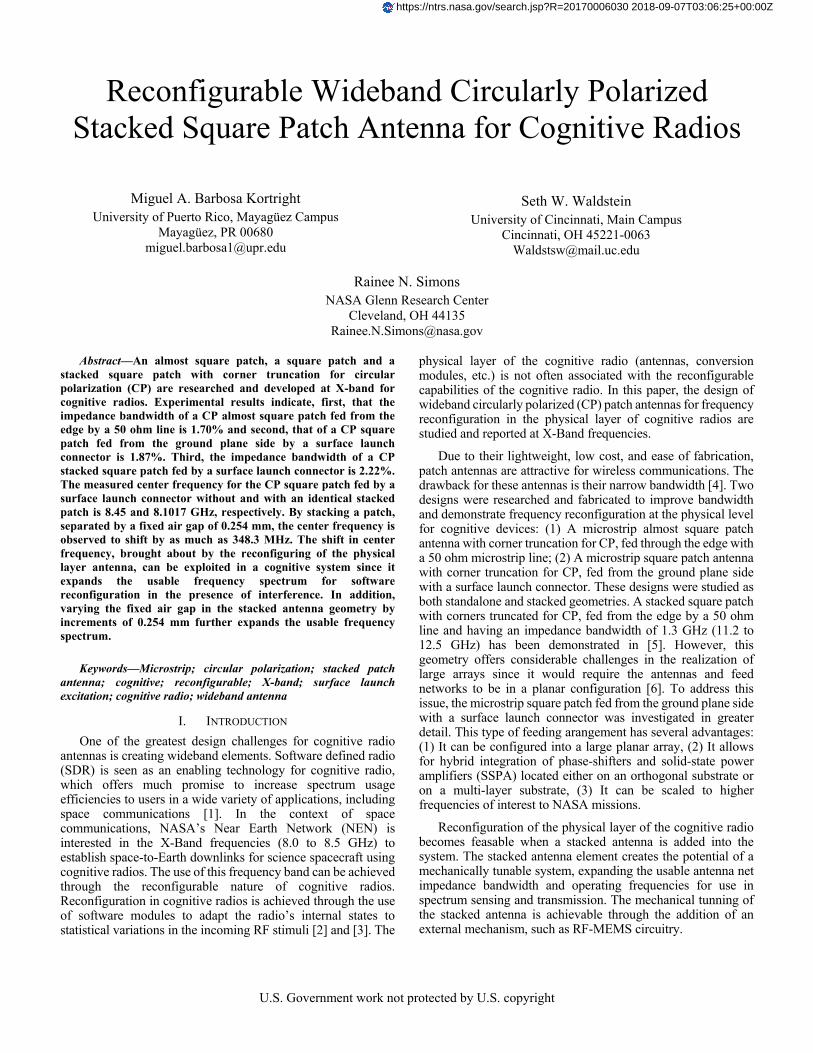
D. Simulated Results – Radiation Pattern
The starting ground plane size was 6060 mm. When varying the plane size by 30 mm, incrementialy and decrementialy, the directivity and realized gain improve, while the angular width varies. The best directivity and realized gain was achieved when the ground plane size was 3030 mm, therefore the radiation pattern were simulated with that ground plane size.
Figs. 4(a) through (c) shows the simulated radiation pattern in Cartesian coordinates in the two principal planes for the three antenna geometries discussed earlier. The inset in Fig. 4(a) shows the reference cartesian coordinate system.
U.S. Government work not protected by U.S. copyright
Fig. 4. Simulated Radiation Pattern: (a) Almost square patch, (b) Square
patch, (c) Stacked square patch. Ground Plane Variation: (d) Stacked square patch.
Fig. 4(d) shows the effect of ground plane size on the radiation pattern of the stacked square patch antenna. Tables IV and V present a summary of the antenna characteristics that were extracted from Figs. 4(a) through (c). Table VI presents a summary of the effects of the ground plane size on the stacked square patch radiation pattern.
TABLE IV. SUMMARY OF CST SIMULATED RADIATION PATTERN WITH PHI EQUAL TO NINETY
Directivity (dBi) Realized Gain (dB)
3 dB Angular Width (Deg.)
Standalone Almost Square Patch, Fed From Edge
7.65
6.7
76.4
Standalone Square Patch, Fed Through Back With Surface Launch Connector
7.45
6.75
76.6
Stacked Square Patch, Fed Through Back With Surface Launch Connector
7.53
7.1
76.1
TABLE V. SUMMARY OF CST SIMULATED RADIATION PATTERN WITH PHI EQUAL TO ZERO
Directivity (dBi) Realized Gain (dB)
3 dB Angular Width (Deg.)
Standalone Almost Square Patch, Fed From Edge
7.65
6.7
75
Standalone Square Patch, Fed Through Back With Surface Launch Connector
7.45
6.75
77
Stacked Square Patch, Fed Through Back With Surface Launch Connector
7.53
7.1
76.7
TABLE VI. SUMMARY OF CST SIMULATED GROUND PLANE VARIATION FOR STACKED SQUARE PATCH AND PHI EQUAL TO NINETY
Directivity (dBi) Realized Gain (dB)
3 dB Angular Width (Deg.)
Ground Plane Size 3030 mm
7.53 7.1 76.1
Ground Plane Size 6060 mm
5.25 4.81 92.5
Ground Plane Size 9090 mm
7.36 6.92 64.6
U.S. Government work not protected by U.S. copyright
III. MICROSTRIP PATCH ANTENNA FABRICATION AND
CHARACTERIZATION
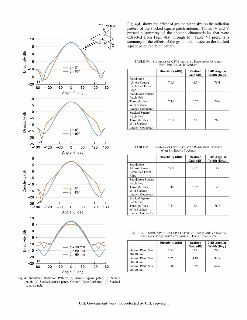
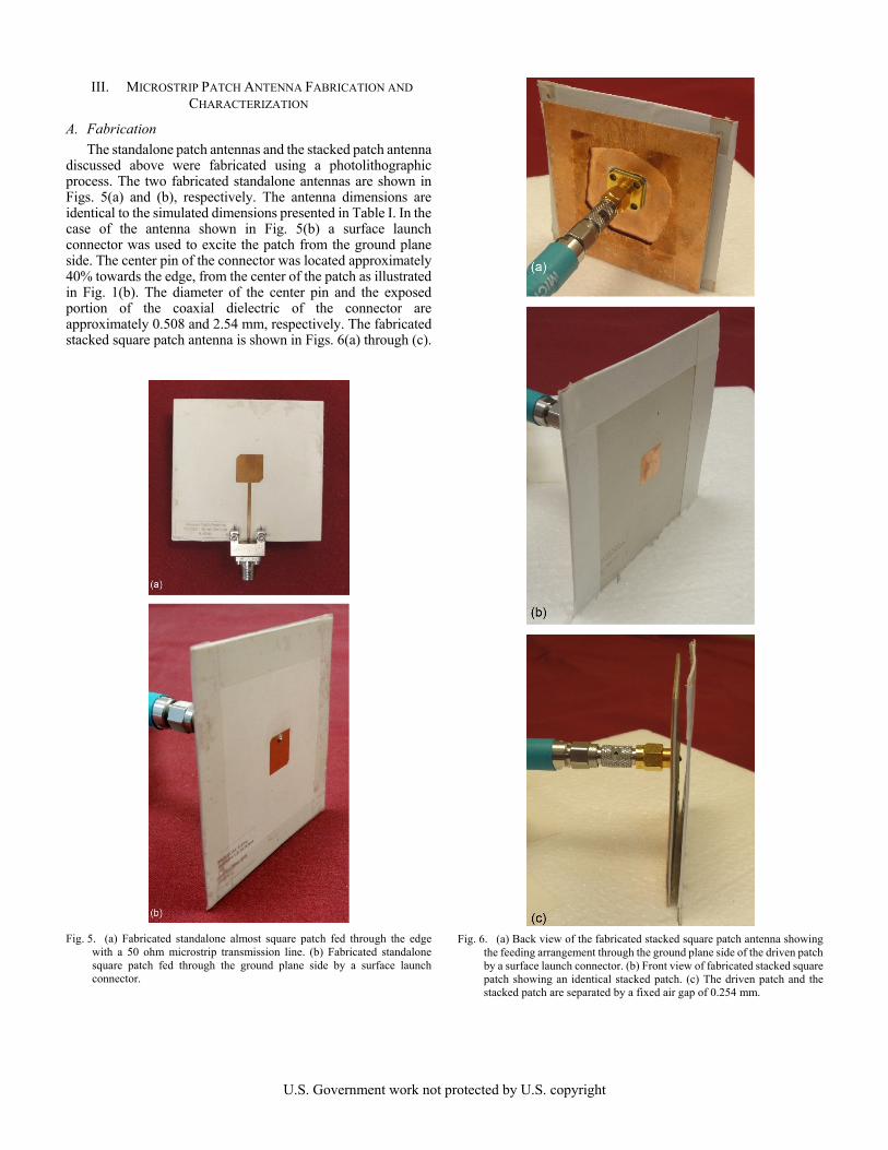
A. Fabrication
The standalone patch antennas and the stacked patch antenna discussed above were fabricated using a photolithographic process. The two fabricated standalone antennas are shown in Figs. 5(a) and (b), respectively. The antenna dimensions are identical to the simulated dimensions presented in Table I. In the case of the antenna shown in Fig. 5(b) a surface launch connector was used to excite the patch from the ground plane side. The center pin of the connector was located approximately 40% towards the edge, from the center of the patch as illustrated in Fig. 1(b). The diameter of the center pin and the exposed portion of the coaxial dielectric of the connector are approximately 0.508 and 2.54 mm, respectively. The fabricated stacked square patch antenna is shown in Figs. 6(a) through (c).
Fig. 5. (a) Fabricated standalone almost square patch fed through the edge
with a 50 ohm microstrip transmission line. (b) Fabricated standalone square patch fed through the ground plane side by a surface launch connector.
Fig. 6. (a) Back view of the fabricated stacked square patch antenna showing
the feeding arrangement through the ground plane side of the driven patch by a surface launch connector. (b) Front view of fabricated stacked square patch showing an identical stacked patch. (c) The driven patch and the stacked patch are separated by a fixed air gap of 0.254 mm.

U.S. Government work not protected by U.S. copyright
B. Characterization
The test setup for characterizing the return loss of the standalone and the stacked patch antennas consisted of an Agilent Technologies E8363B Vector Network Analyzer with phase stable measurement cables. The measured S11 for the two standalone antennas and the stacked antenna are superimposed on the simulated results in Figs. 3(a) through (c), respectively. The experimental data extracted from these figures are summarized in Table VII.
TABLE VII. SUMMARY OF EXPERIMENTAL DATA FOR THE STANDALONE AND STACKED PATCH ANTENNAS. THE AIR GAP IS 0.254 MM IN THE CASE
OF STACKED PATCHES
f0 (GHz)
Return Loss (dB)
fL (GHz)
fH (GHz)
BW = fH - fL (MHz)
BW/f0 (%)
Standalone Almost Square Patch, Fed From Edge
8.46 17.5402 8.385 8.529 144 1.7
Standalone Square Patch, Fed Through Back With Surface Launch Connector
8.45 19.7545 8.3675 8.5255 158 1.87
Stacked Square Patch, Fed Through Back With Surface Launch Connector
8.1017 25.7 8.0204 8.2005 180.1 2.22
Experiments show that the impedance bandwidth of the
standalone antenna fed from the edge by a 50 ohm line is 1.70% and that of the antenna fed from the ground plane side by a surface launch connector is 1.87%. In addition, the impedance bandwidth of the stacked square patch fed from the ground plane side by a surface launch connector is 2.22%. These results indicate that the surface launch type of excitation results in larger impedance bandwidth when compared to edge feeding. Furthermore, the measured center frequency for the square patch excited by a surface launch connector without and with a stacked patch is 8.45 and 8.1017 GHz, respectively. Thus by stacking a patch, separated by a fixed air gap of 0.254 mm, the center frequency is observed to shift by as much as 348.3 MHz (4.12%). Moreover, the simulated and measured results are within 1.24% in all three cases and therefore, considered to be in excellent agreement. The experimental validation of the observed simulated frequency shift discussed earlier strengthens the case for the feasibility in using an external mechanism to reconfigure the stacked antennas in the physical layer of a cognitive radio. The fixed air gap was manually moved in increments of 0.254 mm and was in agreement with the behavior discussed in the simulated results.
IV. ANTENNA FREQUENCY RECONFIGURATION IN
COGNITIVE RADIOS
The shift in the center frequency when a stacked element is added to the standalone element, as discussed above, would enable the reconfiguration of the operating frequency in the physical layer of the cognitive radio to be plausible by way of an external mechanism. The spectrum sensing portion of the cognitive radio would be used initially to identify spectrum holes in the designated band of frequencies and then the software would reconfigure the internal states of the radio to become functional in the available spectrum. The external mechanism would reconfigure the antenna geometry at the physical level of the cognitive radio to be able to transmit at the available spectrum.
CST simulations showed that by increasing the air gap from its initial value of 0.254 mm to five times the initial value (1.27 mm), the central frequency of the stacked patch can be reconfigured from 8.076 to 8.143 GHz. Beyond 1.27 mm, the driven patch and the stacked patch begin to decouple and the air gap has no significant influence on the central frequency. Taking the above simulated central frequency shift and the air gap dimensions into account, the central frequency sensitivity of the system is on the order of 5.28 MHz per 100 microns change in air gap dimensions.
V. FUTURE WORK
A. Frequency Reconfiguration With MEMS Devices
The rate of change and the precision with which the air gap dimensions can be reconfigured are dependent on the capabilities of the external tuning mechanism. Electrostatically actuated MEMS devices [11,12], electro-active polymers/shape memory alloy actuators [13], magnetic actuators [14], and displacement multipliers [15] when integrated with printed antennas have been demonstrated as a viable technology to reconfigure the antenna characteristics. However, this topic will be investigated in greater detail and results will be presented in a future paper.
B. Polarization Reconfiguration With Semiconductor Devices
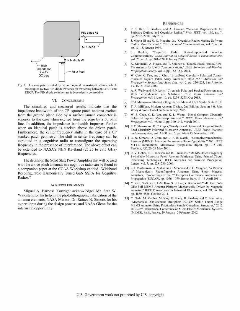
A scheme to implement polarization reconfigurability of a CP square patch antenna is illustrated in Fig. 7. The two orthogonal feeds are coupled to the patch via two PIN diodes, which can be biased independently. In the arrangement shown, when PIN diode #1 is turned ON and PIN diode #2 is in the OFF state, the antenna is similar to the patch antenna illustrated in Fig. 1(a). The antenna radiates a LHCP signal. When PIN diode #1 is turned OFF and PIN diode #2 is turned ON, the antenna radiates a RHCP signal. Polarization reconfiguration would be useful in a cognitive radio because it would enable data transmission in both LHCP and RHCP, which would further expand the capabilities of the cognitive radio.
U.S. Government work not protected by U.S. copyright
Fig. 7. A square patch excited by two orthogonal microstrip feed lines, which
are coupled by two PIN diode switches for switching between LHCP and RHCP. The PIN diode switches are independently controlable.
VI. CONCLUSIONS
The simulated and measured results indicate that the impedance bandwidth of the CP square patch antenna excited from the ground plane side by a surface launch connector is superior to the case when excited from the edge by a 50 ohm line. In addition, the impedance bandwidth improves further when an identical patch is stacked above the driven patch. Furthermore, the center frequency shifts in the case of a CP stacked patch geometry. The shift in center frequency can be exploited in a cognitive radio to reconfigure the operating frequency in the presence of interference. The above effort can be extended to NASA’s NEN Ka-Band (25.25 to 27.5 GHz) frequencies.
The details on the Solid State Power Amplifier that will be used with the above patch antennas in a cognitive radio can be found in a companion paper at the CCAA Workshop entitled “Wideband Reconfigurable Harmonically Tuned GaN SSPA for Cognitive Radios.”
ACKNOWLEDGMENTS
Miguel A. Barbosa Kortright acknowledges Mr. Seth W. Waldstein for his help in the photolithographic fabrication of the antenna elements, NASA Mentor, Dr. Rainee N. Simons for his expert input during the design process, and NASA Glenn for the internship opportunity.
REFERENCES [1] P. S. Hall, P. Gardner, and A, Faraone, “Antenna Requirements for
Software Defined and Cognitive Radios,” Proc. IEEE, vol. 100, no. 7, pp. 2262–2270, July 2012.
[2] J. Mitola III and G. Q. Maguire, Jr., “Cognitive Radio: Making Software Radios More Personal,” IEEE Personal Communications, vol. 6, no. 4, pp. 13–18, August 1999.
[3] S. Haykin, “Cognitive Radio: Brain-Empowered Wireless Communications,” IEEE Journal on Selected Areas in communications, vol. 23, no. 2, pp. 201–220, February 2005.
[4] K. Kiminami, A. Hirata, and T. Shiozawa, “Double-Sided Printed Bow-Tie Antenna for UWB Communications,” IEEE Antennas and Wireless Propagation Letters, vol. 3, pp. 152–153, 2004.
[5] W. Choi, C. Pyo, and J. Choi, “Broadband Circularly Polarized Corner-truncated Square Patch Array Antenna,” 2002 IEEE Antennas and Propagation Society Inter Symp Dig., vol. 2, pp. 220–223, San Antonio, Tx, 16–21 June 2002.
[6] A. R. Weily and N. Nikolic, “Circularly Polarized Stacked Patch Antenna With Perpendicular Feed Substrate,” IEEE Trans Antennas and Propagation, vol. 61, no. 10, pp. 5274–5278, Oct 2013.
[7] CST Microwave Studio Getting Started Manual, CST Studio Suite 2010.
[8] T. A. Milligan, Modern Antenna Design, 2nd Edition, Section 6-6, John Wiley & Sons, Hoboken, New Jersey, 2005.
[9] W.-S. Chen, C.-K. Wu, and K.-L. Wong, “Novel Compact Circularly Polarized Square Microstrip Antenna,” IEEE Trans Antennas and Propagation, vol. 49, no. 3, pp. 340–342, March 2001.
[10] P. C. Sharma and K. C. Gupta, “Analysis and Optimized Design of Single Feed Circularly Polarized Microstrip Antennas,” IEEE Trans Antennas and Propagation, vol. AP-31, no. 6, pp. 949–955, November 1983.
[11] R. N. Simons, D. Chun and L. P. B. Katehi, “Microelectromechanical Systems (MEMS) Actuators for Antenna Reconfigurability,” 2001 IEEE MTT-S International Microwave Symposium Digest, pp. 215–218, Phoneix, AZ, 20–24 May 2001.
[12] R. V. Goteti, R. E. Jackson and R. Ramadoss, “MEMS-Based Frequency Switchable Microstrip Patch Antenna Fabricated Using Printed Circuit Processing Techniques,” IEEE Antennas and Wireless Propagation Letters, vol. 5, pp. 228–230, 2006.
[13] S. J. Mazlouman, A. Mahanfar, C. Menon and R. G. Vaughan, “A Review of Mechanically Reconfigurable Antennas Using Smart Material Actuators,” Proceedings of the 5th European Conference Antennas and Propagation (EUCAP), pp. 1076–1079, Rome, Italy, 11–15 April 2011.
[14] Y. Kim, N.-G. Kim, J.-M. Kim, S. H. Lee, Y. Kwon and Y.-K. Kim, “60-GHz Full MEMS Antenna Platform Mechanically Driven by Magnetic Actuator,” IEEE Transactions on Industrial Electronics, vol. 58, no. 10, pp. 4830–4836, October 2011.
[15] Y. Nada, M. Medhat, M. Nagi, F. Marty, B. Saadany and T. Bourouina, “Mechanical Displacement Multiplier: 250 uM Stable Travel Range MEMS Actuator Using Frictionless Simple Compliant Structures,” 2012 IEEE 25th International Conference on Micro Electro Mechanical Systems (MEMS), Paris, France, 29 January–2 February 2012.