records of revisionpdf.masters.com.pl/powertip/pe320240wrf-001-hq.pdf · 3.1 quality assurance flow...
TRANSCRIPT
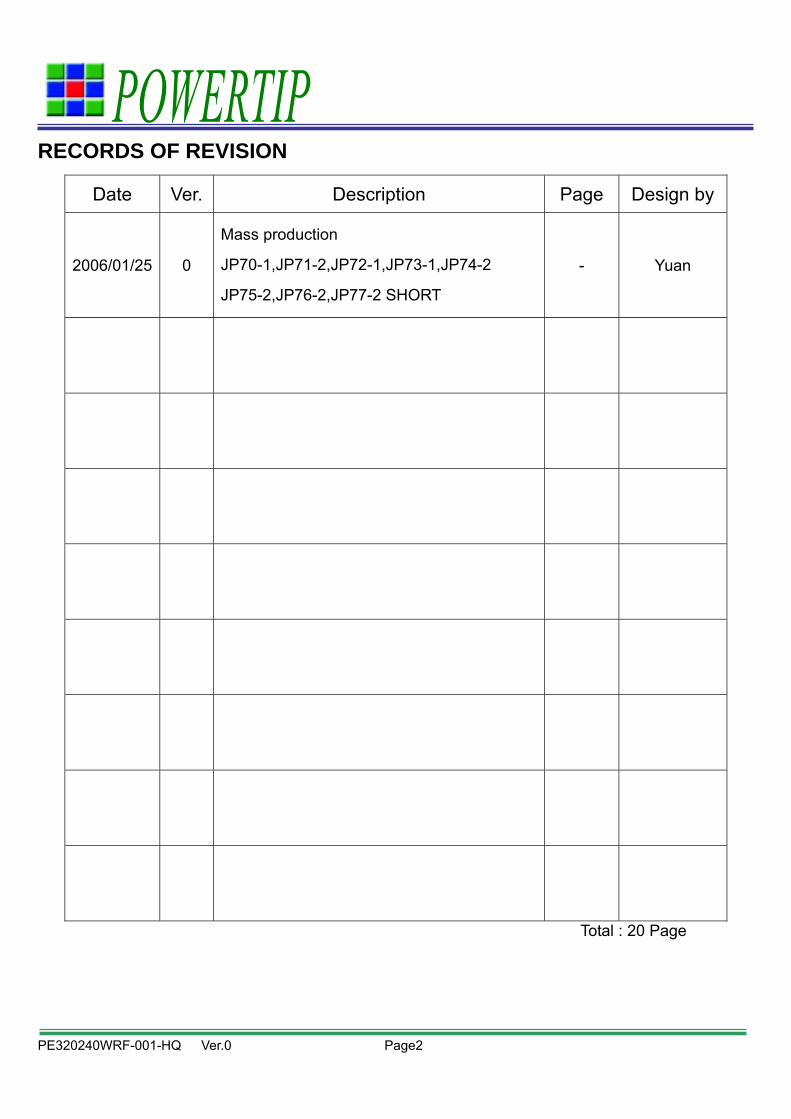
PE320240WRF-001-HQ Ver.0 Page2
RECORDS OF REVISION
Date Ver. Description Page Design by
2006/01/25 0
Mass production
JP70-1,JP71-2,JP72-1,JP73-1,JP74-2
JP75-2,JP76-2,JP77-2 SHORT
- Yuan
Total : 20 Page
PE320240WRF-001-HQ Ver.0 Page3
Contents 1. SPECIFICATIONS 1.1 Features 1.2 Mechanical Specifications 1.3 Absolute Maximum Ratings 1.4 DC Electrical Characteristics 1.5 Optical Characteristics 1.6 Backlight Characteristics 2. MODULE STRUCTURE 2.1 Counter Drawing 2.2 Interface Pin Description 2.3 Timing Characteristics 2.4 Command Table
3. QUALITY ASSURANCE SYSTEM 3.1 Quality Assurance Flow Chart 3.2 Inspection Specification
4. RELIABILITY TEST 4.1 Reliability Test Condition
5. PRECAUTION RELATING PRODUCT HANDLING 5.1 Safety 5.2 Handling 5.3 Storage 5.4 Terms of Warranty Appendix :
1. LCM drawing 2. Package
Note:For detailed information please refer to IC data sheet:
Sitronix ST8016 , ST8024
PE320240WRF-001-HQ Ver.0 Page4
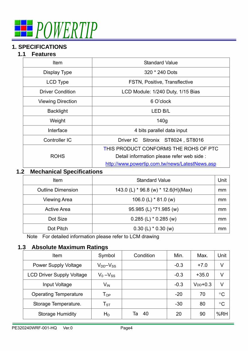
1. SPECIFICATIONS 1.1 Features
Item Standard Value
Display Type 320 * 240 Dots
LCD Type FSTN, Positive, Transflective
Driver Condition LCD Module: 1/240 Duty, 1/15 Bias
Viewing Direction 6 O’clock
Backlight LED B/L
Weight 140g
Interface 4 bits parallel data input
Controller IC Driver IC Sitronix ST8024 , ST8016
ROHS THIS PRODUCT CONFORMS THE ROHS OF PTC
Detail information please refer web side : http://www.powertip.com.tw/news/LatestNews.asp
1.2 Mechanical Specifications Item Standard Value Unit
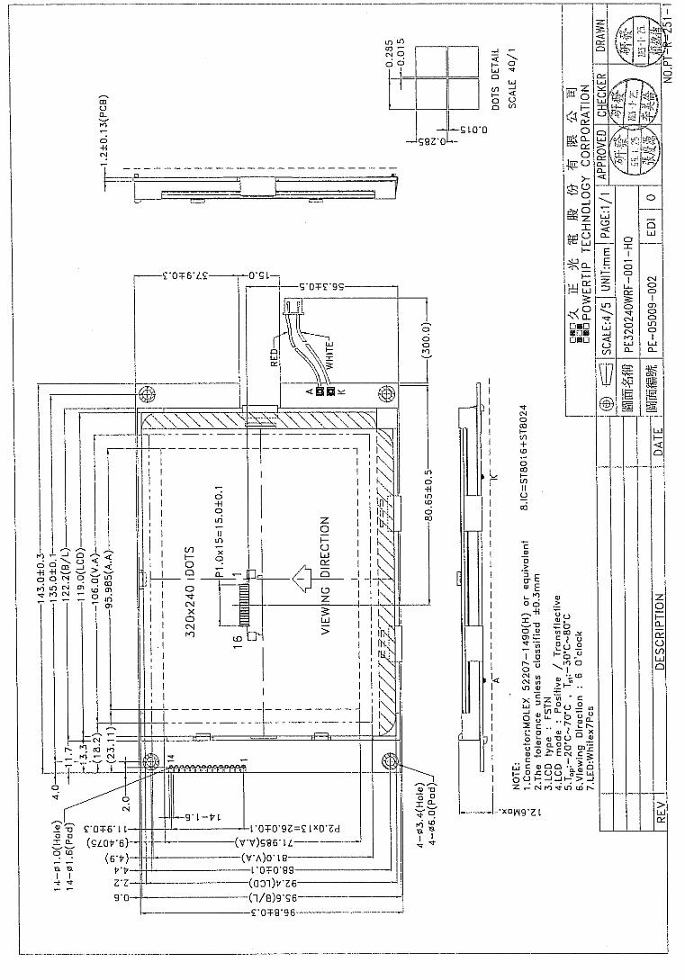
Outline Dimension 143.0 (L) * 96.8 (w) * 12.6(H)(Max) mm
Viewing Area 106.0 (L) * 81.0 (w) mm
Active Area 95.985 (L) *71.985 (w) mm
Dot Size 0.285 (L) * 0.285 (w) mm
Dot Pitch 0.30 (L) * 0.30 (w) mmNote:For detailed information please refer to LCM drawing
1.3 Absolute Maximum Ratings Item Symbol Condition Min. Max. Unit
Power Supply Voltage VDD–VSS - -0.3 +7.0 V
LCD Driver Supply Voltage V0 –VSS - -0.3 +35.0 V
Input Voltage VIN - -0.3 VDD+0.3 V
Operating Temperature TOP - -20 70 °C
Storage Temperature. TST - -30 80 °C
Storage Humidity HD Ta<40 20 90 %RH
PE320240WRF-001-HQ Ver.0 Page5
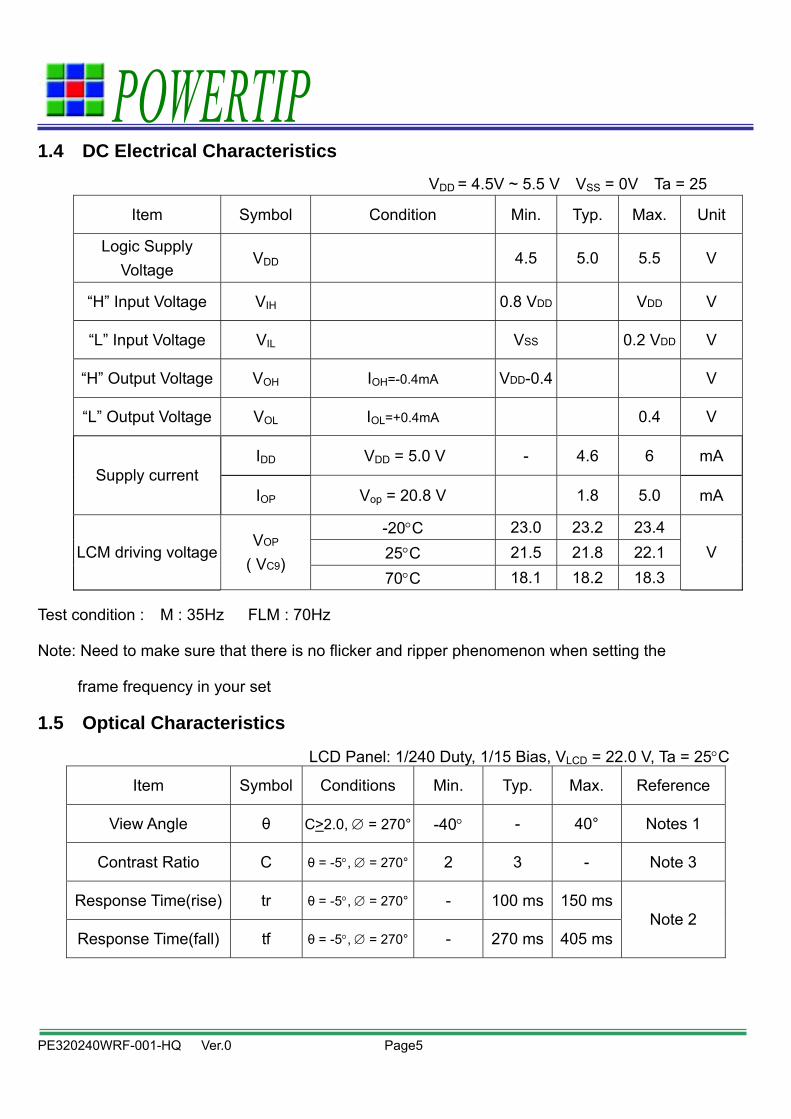
1.4 DC Electrical Characteristics VDD = 4.5V ~ 5.5 V,VSS = 0V,Ta = 25
Item Symbol Condition Min. Typ. Max. Unit
Logic Supply Voltage
VDD - 4.5 5.0 5.5 V
“H” Input Voltage VIH - 0.8 VDD - VDD V
“L” Input Voltage VIL - VSS - 0.2 VDD V
“H” Output Voltage VOH IOH=-0.4mA VDD-0.4 - - V
“L” Output Voltage VOL IOL=+0.4mA - - 0.4 V
IDD VDD = 5.0 V - 4.6 6 mA Supply current
IOP Vop = 20.8 V 1.8 5.0 mA
-20°C 23.0 23.2 23.4 25°C 21.5 21.8 22.1 LCM driving voltage
VOP
( VC9) 70°C 18.1 18.2 18.3
V
Test condition : M : 35Hz FLM : 70Hz
Note: Need to make sure that there is no flicker and ripper phenomenon when setting the
frame frequency in your set
1.5 Optical Characteristics
LCD Panel: 1/240 Duty, 1/15 Bias, VLCD = 22.0 V, Ta = 25°C
Item Symbol Conditions Min. Typ. Max. Reference
View Angle θ C>2.0, ∅ = 270° -40° - 40° Notes 1
Contrast Ratio C θ = -5°, ∅ = 270° 2 3 - Note 3
Response Time(rise) tr θ = -5°, ∅ = 270° - 100 ms 150 ms
Response Time(fall) tf θ = -5°, ∅ = 270° - 270 ms 405 ms Note 2

PE320240WRF-001-HQ Ver.0 Page6
Note 1.
Optical characteristics-2
Viewing angle
Front (6H)φ=270°
Rear (12H)φ=90°
Right (3H)φ=0°
Left (9H)φ=180°
θL
Viewing angle
Top (θ=0°)
θR
θ-
θ+

PE320240WRF-001-HQ Ver.0 Page7
Note 2.
Optical characteristics-3Fig.2 Definition of response time
Positive Type
Selected waveformNo selected waveform No selected waveform
100% 90%
10%
TfTr
Transmittance
Negative Type
100% 90%
10%
TfTr
No selected Selected waveformNo selected waveform
Transmittance
PE320240WRF-001-HQ Ver.0 Page8
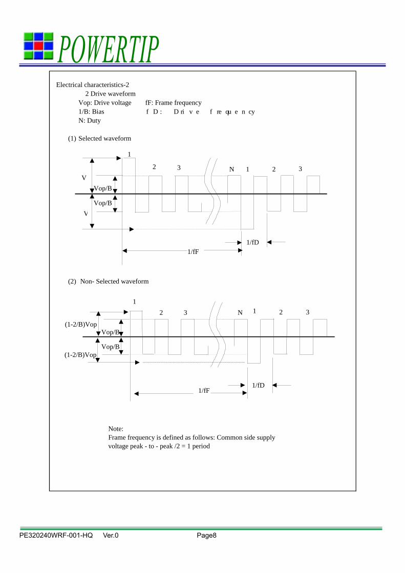
Electrical characteristics-2※2 Drive waveformVop: Drive voltage fF: Frame frequency1/B: Bias fD: Drive frequencyN: Duty
(1) Selected waveform
(2) Non- Selected waveform
1V
Vop/B
Vop/B
V
1/fF1/fD
32N32
1
Note:Frame frequency is defined as follows: Common side supplyvoltage peak - to - peak /2 = 1 period
Vop/B
1/fF1/fD
321N321
(1-2/B)Vop
Vop/B(1-2/B)Vop
PE320240WRF-001-HQ Ver.0 Page9
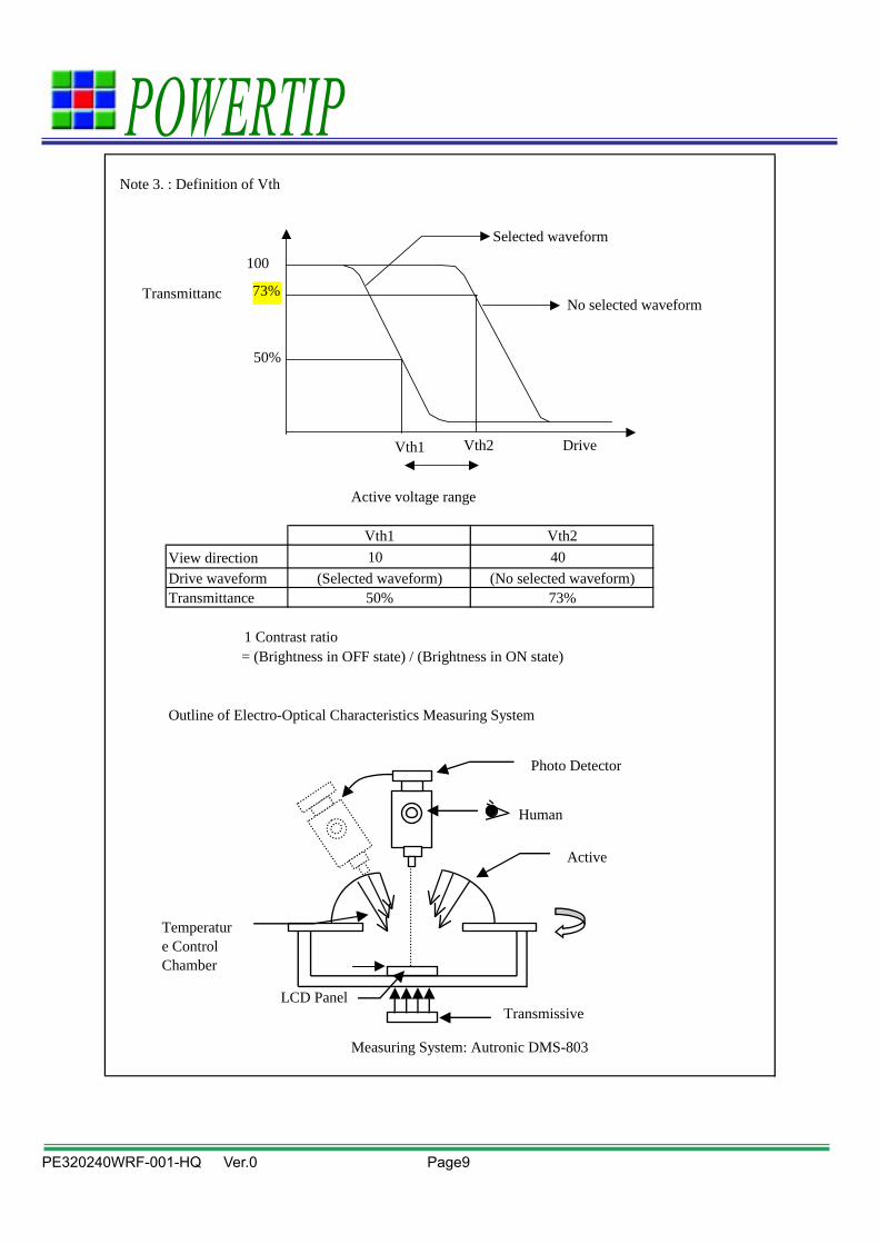
Note 3. : Definition of Vth
Active voltage range
View directionDrive waveformTransmittance
※1 Contrast ratio= (Brightness in OFF state) / (Brightness in ON state)
Outline of Electro-Optical Characteristics Measuring System
Measuring System: Autronic DMS-803
50%(No selected waveform)
73%
Vth240°
(Selected waveform)
Vth110°
Selected waveform
No selected waveform
DriveVth2Vth1
Transmittanc
100
73%
50%
正讀
θ
ψ
Human
Photo Detector
LCD PanelTransmissive
Temperature ControlChamber
Active
PE320240WRF-001-HQ Ver.0 Page10
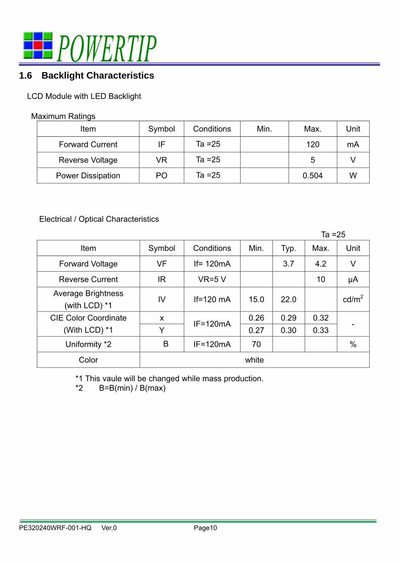
1.6 Backlight Characteristics
LCD Module with LED Backlight
Maximum Ratings Item Symbol Conditions Min. Max. Unit
Forward Current IF Ta =25 - 120 mA
Reverse Voltage VR Ta =25 - 5 V
Power Dissipation PO Ta =25 - 0.504 W
Electrical / Optical Characteristics
Ta =25
Item Symbol Conditions Min. Typ. Max. Unit
Forward Voltage VF If= 120mA - 3.7 4.2 V
Reverse Current IR VR=5 V - - 10 µA
Average Brightness (with LCD) *1
IV If=120 mA 15.0 22.0 - cd/m2
x 0.26 0.29 0.32 CIE Color Coordinate (With LCD) *1 Y
IF=120mA 0.27 0.30 0.33
-
Uniformity *2 B IF=120mA 70 - - %
Color white
*1 This vaule will be changed while mass production. *2:B=B(min) / B(max)
PE320240WRF-001-HQ Ver.0 Page11
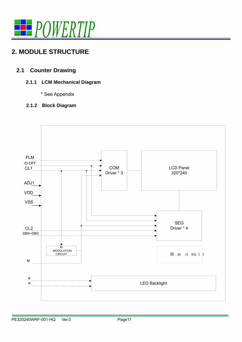
2. MODULE STRUCTURE
2.1 Counter Drawing
2.1.1 LCM Mechanical Diagram
* See Appendix
2.1.2 Block Diagram
COMDriver * 3
LCD Panel320*240
SEGDriver * 4
FLM/D-OFFCL1
DB0~DB3CL2
MMODULATION
CIRCUIT
VDD
LED BacklightKA
VSS
ADJ1
M
Bias circuit
PE320240WRF-001-HQ Ver.0 Page12
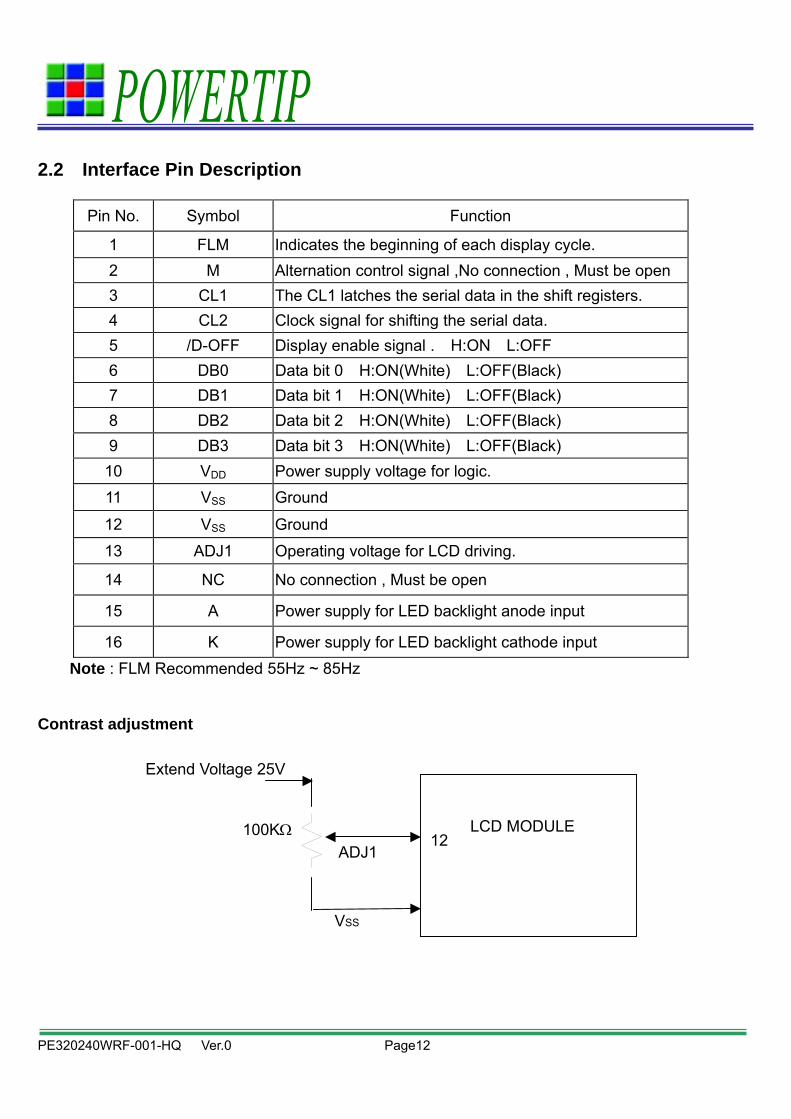
2.2 Interface Pin Description
Pin No. Symbol Function
1 FLM Indicates the beginning of each display cycle. 2 M Alternation control signal ,No connection , Must be open 3 CL1 The CL1 latches the serial data in the shift registers. 4 CL2 Clock signal for shifting the serial data. 5 /D-OFF Display enable signal . H:ON L:OFF 6 DB0 Data bit 0 H:ON(White) L:OFF(Black) 7 DB1 Data bit 1 H:ON(White) L:OFF(Black) 8 DB2 Data bit 2 H:ON(White) L:OFF(Black) 9 DB3 Data bit 3 H:ON(White) L:OFF(Black)
10 VDD Power supply voltage for logic. 11 VSS Ground
12 VSS Ground
13 ADJ1 Operating voltage for LCD driving.
14 NC No connection , Must be open
15 A Power supply for LED backlight anode input
16 K Power supply for LED backlight cathode input Note : FLM Recommended 55Hz ~ 85Hz
Contrast adjustment
Extend Voltage 25V
LCD MODULE ADJ1
12
100KΩ
VSS
PE320240WRF-001-HQ Ver.0 Page13
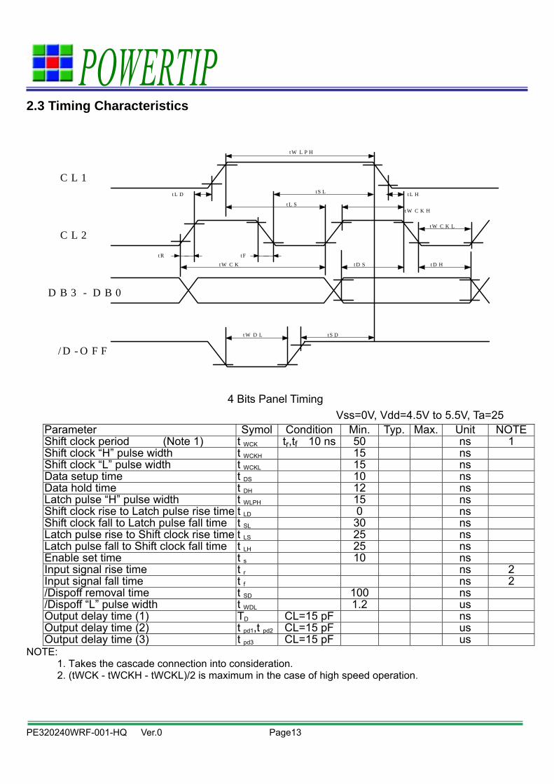
2.3 Timing Characteristics
4 Bits Panel Timing Vss=0V, Vdd=4.5V to 5.5V, Ta=25
Parameter Symol Condition Min. Typ. Max. Unit NOTEShift clock period (Note 1) t WCK tr,tf≦10 ns 50 ns 1 Shift clock “H” pulse width t WCKH 15 ns Shift clock “L” pulse width t WCKL 15 ns Data setup time t DS 10 ns Data hold time t DH 12 ns Latch pulse “H” pulse width t WLPH 15 ns Shift clock rise to Latch pulse rise time t LD 0 ns Shift clock fall to Latch pulse fall time t SL 30 ns Latch pulse rise to Shift clock rise time t LS 25 ns Latch pulse fall to Shift clock fall time t LH 25 ns Enable set time t s 10 ns Input signal rise time t r ns 2 Input signal fall time t f ns 2 /Dispoff removal time t SD 100 ns /Dispoff “L” pulse width t WDL 1.2 us Output delay time (1) TD CL=15 pF ns Output delay time (2) t pd1,t pd2 CL=15 pF us Output delay time (3) t pd3 CL=15 pF us
NOTE: 1. Takes the cascade connection into consideration. 2. (tWCK - tWCKH - tWCKL)/2 is maximum in the case of high speed operation.
C L 1
C L 2
D B 3 - D B 0
/ D - O F F
t W L P H
t L D t S L
t L S
t R t F
t W C K t D S t D H
t W D L t S D
t L H
t W C K H
t W C K L
PE320240WRF-001-HQ Ver.0 Page14
PE320240WRF-001-HQ Ver.0 Page15
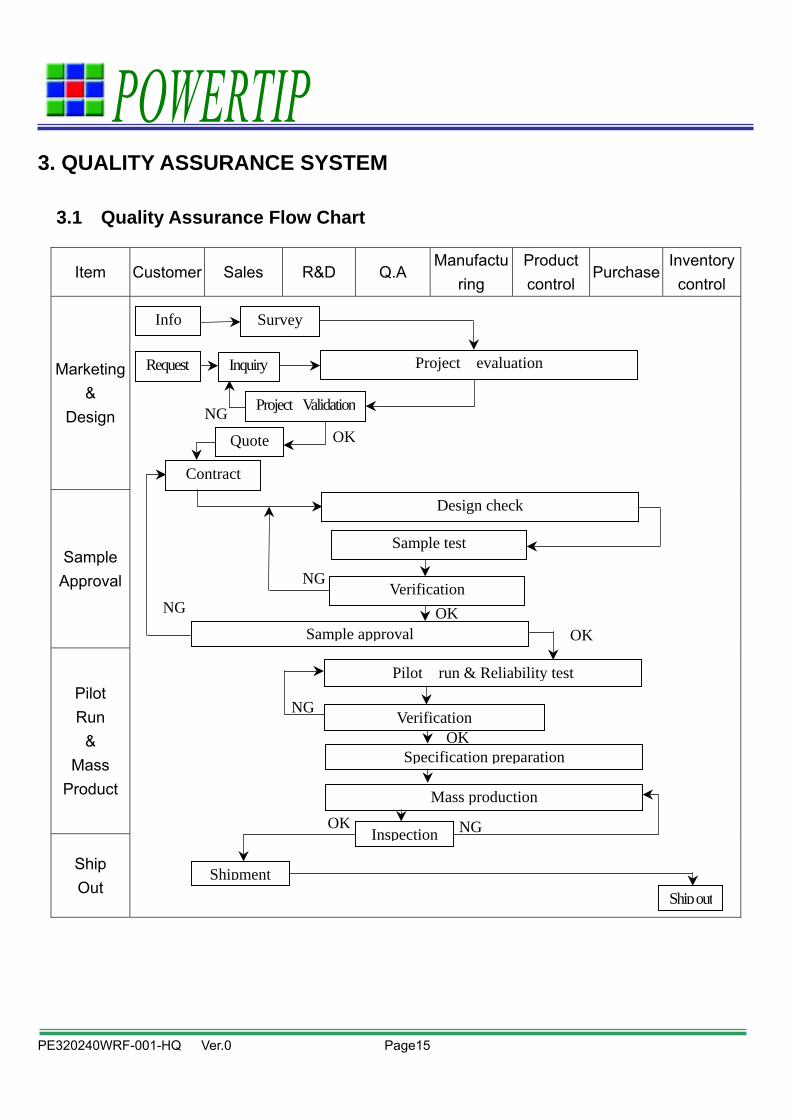
3. QUALITY ASSURANCE SYSTEM
3.1 Quality Assurance Flow Chart
Item Customer Sales R&D Q.A Manufactu
ring Product control
PurchaseInventory control
Marketing &
Design
Sample Approval
Pilot Run
& Mass
Product
Ship Out
OK
Request
Info Survey
Inquiry Project evaluation
Project Validation
Quote OK NG
Contract
Design check
Sample test
Verification
Sample approval
NG
NG
Pilot run & Reliability test
Verification
Specification preparation OK
Mass production
Inspection NGOK
Shipment
NG
Ship out
OK

PE320240WRF-001-HQ Ver.0 Page16
Item Customer Sales R&D Q.A Manufact
uring Product control
PurchaseInventory
control
Sales Service
Q.A Activity
1. ISO 9001 Maintenance Activities 2. Process improvement proposal 3. Equipment calibration 4. Education And Training Activities 5. Standardization Management
Info Claim
Failure analysis
Corrective action
Tracking
Analysis report

PE320240WRF-001-HQ Ver.0 Page17
3.2 Inspection Specification Inspection Standard:MIL-STD-105E Table Normal Inspection Single Sampling Level Ⅱ。 Equipment:Gauge、MIL-STD、Powertip Tester、Sample。 IQC Defect Level:Major Defect AQL 0.4; Minor Defect AQL 1.5。 FQC Defect Level:100% Inspection。 OUT Going Defect Level:Sampling。 Specification:
NO Item Specification Judge Level
1 Part Number The part number is inconsistent with work order of production N.G. Major
2 Quantity The quantity is inconsistent with work order of production N.G. Major
The display lacks of some patterns. N.G. MajorMissing line. N.G. MajorThe size of missing dot, A is>1/2 Dot size N.G. MajorThere is no function. N.G. Major
3
Electronic characteristics of
LCM A=( L + W )÷2
Output data is error N.G. MajorMaterial is different with work order of production N.G. MajorLCD is assembled in inverse direction N.G. MajorBezel is assembled in inverse direction N.G. MajorShadow is within LCD viewing area + 0.5 mm N.G. MajorThe diameter of dirty particle, A is>0.4 mm N.G. MinorDirty particle length is >3.0mm, and 0.01mm<width ≦0.05mm N.G. Minor
Display is without protective film N.G. MinorConductive rubber is over bezel 1mm N.G. MinorPolarizer exceeds over viewing area of LCD N.G. MinorArea of bubble in polarizer, A>1.0mm, the number of bubble is >1 piece. N.G. Minor
4
Appearance of LCD
A=( L + W )÷2
Dirty particle (Including
scratch、bubble )
0.4mm<Area of bubble in polarizer, A<1.0mm, the number of bubble is >4 pieces. N.G. Minor
Burned area or wrong part number is on PCB N.G. MajorThe symbol, character, and mark of PCB are unidentifiable. N.G Minor
The stripped solder mask , A is>1.0mm N.G. Minor0.3mm<stripped solder mask or visible circuit, A <1.0mm, and the number is ≧4 pieces N.G. Minor
There is particle between the circuits in solder mask N.G MinorThe circuit is peeled off or cracked N.G MinorThere is any circuits risen or exposed. N.G Minor0.2mm<Area of solder ball, A is ≦0.4mm The number of solder ball is ≧3 pieces N.G Minor
5 Appearance of
PCB A=( L + W )÷2
The magnitude of solder ball, A is >0.4mm. N.G Minor

PE320240WRF-001-HQ Ver.0 Page18
NO Item Specification Judge Level
The shape of modeling is deformed by touching. N.G. MajorInsufficient epoxy: Circuit or pad of IC is visible N.G. MinorExcessive epoxy: Diameter of modeling is >20mm or height is >2.5mm N.G. Minor6
Appearance of molding
A=( L + W )÷2 The diameter of pinhole in modeling, A is >0.2mm. N.G. MinorThe folding angle of frame must be >45° +10° N.G. MinorThe area of stripped electroplate in top-view of frame, A is >1.0mm. N.G. Minor
Rust or crack is (Top view only) N.G. Minor7
Appearance of frame
A=( L + W )÷2 The scratched width of frame is >0.06mm. (Top view only) N.G. Minor
The color of backlight is nonconforming N.G. MajorBacklight can’t work normally. N.G. MajorThe LED lamp can’t work normally N.G. MajorThe unsoldering area of pin for backlight, A is >1/2 solder joint area. N.G. Minor
8
Electrical characteristic of
backlight
A=( L + W )÷2 The height of solder pin for backlight is >2.0mm N.G. MinorThe mark or polarity of component is unidentifiable. N.G. MinorThe height between bottom of component and surface of the PCB is floating >0.7mm N.G. Minor
D>1/4W W D
D’ Pad
N.G. Minor
End solder joint width, D’ is >50% width of component termination or width of pad N.G. Minor
Side overhang, D is >25% width of component termination. N.G. Minor
Component is cracked, deformed, and burned, etc. N.G. MinorThe polarity of component is placed in inverse direction. N.G. Minor
10 Assembly parts A=( L + W )÷2
Maximum fillet height of solder extends onto the component body or minimum fillet height is <0.5mm.
N.G. Minor
PE320240WRF-001-HQ Ver.0 Page19
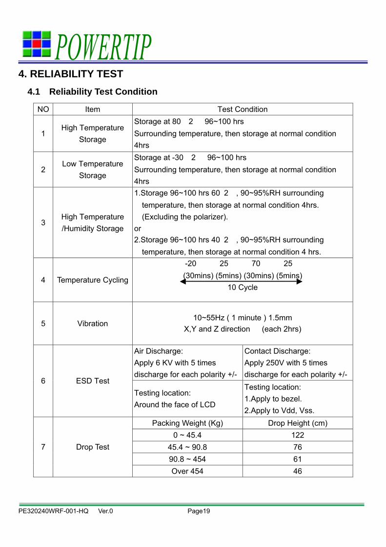
4. RELIABILITY TEST
4.1 Reliability Test Condition
NO Item Test Condition
1 High Temperature
Storage
Storage at 80 ±2 96~100 hrs Surrounding temperature, then storage at normal condition 4hrs
2 Low Temperature
Storage
Storage at -30 ±2 96~100 hrs Surrounding temperature, then storage at normal condition 4hrs
3 High Temperature /Humidity Storage
1.Storage 96~100 hrs 60±2, 90~95%RH surrounding temperature, then storage at normal condition 4hrs.
(Excluding the polarizer). or 2.Storage 96~100 hrs 40±2, 90~95%RH surrounding
temperature, then storage at normal condition 4 hrs.
4 Temperature Cycling
-20 → 25 → 70 → 25 (30mins) (5mins) (30mins) (5mins)
10 Cycle
5 Vibration 10~55Hz ( 1 minute ) 1.5mm
X,Y and Z direction ﹡(each 2hrs)
Air Discharge: Apply 6 KV with 5 times discharge for each polarity +/-
Contact Discharge: Apply 250V with 5 times discharge for each polarity +/-
6 ESD Test Testing location: Around the face of LCD
Testing location: 1.Apply to bezel. 2.Apply to Vdd, Vss.
Packing Weight (Kg) Drop Height (cm) 0 ~ 45.4 122
45.4 ~ 90.8 76 90.8 ~ 454 61
7 Drop Test
Over 454 46

PE320240WRF-001-HQ Ver.0 Page20
5. PRECAUTION RELATING PRODUCT HANDLING 5.1 SAFETY
5.1.1 If the LCD panel breaks , be careful not to get the liquid crystal to touch your skin. 5.1.2 If the liquid crystal touches your skin or clothes , please wash it off immediately by
using soap and water. 5.2 HANDLING
5.2.1 Avoid any strong mechanical shock which can break the glass. 5.2.2 Avoid static electricity which can damage the CMOS LSI—When working with the
module , be sure to ground your body and any electrical equipment you may be using.
5.2.3 Do not remove the panel or frame from the module. 5.2.4 The polarizing plate of the display is very fragile. So , please handle it very
carefully ,do not touch , push or rub the exposed polarizing with anything harder than an HB pencil lead (glass , tweezers , etc.)
5.2.5 Do not wipe the polarizing plate with a dry cloth , as it may easily scratch the surface of plate.
5.2.6 Do not touch the display area with bare hands , this will stain the display area. 5.2.7 Do not use ketonics solvent & aromatic solvent. Use with a soft cloth soaked with
a cleaning naphtha solvent. 5.3 STORAGE 5.3.1 Store the panel or module in a dark place where the temperature is 25 ±5
and the humidity is below 65% RH. 5.3.2 Do not place the module near organics solvents or corrosive gases.
5.3.3 Do not crush , shake , or jolt the module. 5.4 TERMS OF WARRANTY 5.4.1 Applicable warrant period
The period is within thirteen months since the date of shipping out under normal using and storage conditions.
5.4.2 Unaccepted responsibility This product has been manufactured to your company’s specification as a part for use in your company’s general electronic products. It is guaranteed to perform according to delivery specifications. For any other use apart from general electronic equipment , we cannot take responsibility if the product is used in nuclear power control equipment , aerospace equipment , fire and security systems or any other applications in which there is a direct risk to human life and where extremely high levels of reliability are required.