reduction of 1/f noise in mosfets by switched bias …
TRANSCRIPT

MESA+ Research Institute, University of Twente,P.O. Box 217, Enschede, The Netherlands. Phone +31-53-489 2655,
email: [email protected], http://icd.el.utwente.nl
Abstract: Switched Biasing is a new a technique for reducing the 1/f noise in MOSFETS.Conventional techniques, such as chopping or correlated double sampling, reduce the effect of1/f noise in electronic circuits, whereas the Switched Biasing technique reduces the 1/f noiseitself. It exploits an intriguing physical effect: cycling a MOS transistor from strong inversionto accumulation reduces its 1/f noise. In fact the transistor “forgets” its past and thus theselow-frequency noise components. This effect is important, especially in RF circuits where 1/fnoise is often being upconverted, and is thus a serious problem. The history of the(re)discovery of the effect and the main experimental results obtained so far will be reviewed.
I. INTRODUCTION
CMOS ICs nowadays may contain up to several millions of transistors, mainly used indigital circuits, but also in analog and mixed analog-digital interface circuits (e.g. ADC,DAC, pre- and postamplifiers, up- and downconverters between baseband and RF). Ascharge transport in electronic devices is fundamentally accompanied by noise, the behaviourof all MOS transistors is subject to these random variations. These random variationsultimately limit the signal processing capability of transistor circuits, as they put a lowerlimit to the signal that can be processed reliably. Thus noise for instance limits the Signal-to-Noise ratio of analog circuits, resulting in noisy music or noisy TV pictures. In digitaltransmission systems noise introduces bit errors.As noise results from device physics, designers generally consider it as something youcannot change and have to live with. In this paper it will be shown that this is not necessarilytrue for 1/f noise: it will be shown that it is possible to interact with the physical noisegenerating processes in a MOS transistor in such a way that the 1/f noise is reduced. Wediscovered this in a research project aiming at low timing jitter in a CMOS ring oscillator forTV applications. This paper reviews the history of the project and the main results obtainedso far.
II. TIMING JITTER IN CMOS RING OSCILLATORS
Figure 1 shows the clock signal generated by a ring oscillator generating the pixel clock for aPicture-in-Picture (PIP) window on a 100Hz TV screen. The time of zero-crossingdetermines the horizontal positioning of a pixel in the PIP window. Noise of MOStransistors in the oscillator introduces timing uncertainty in the zero-crossings and hencepixel misalignment. In a ring oscillator, subsequent zero-crossings are generated bysubsequent oscillator stages. As every stage introduces its own zero-crossing timinguncertainty, while the transition of one stage starts the transition of the next stage, the totalstandard deviation in the time of zero crossing (total timing jitter or accumulated jitter σT)
Reduction of 1/f Noise in MOSFETsby Switched Bias Techniques
Bram Nauta, Eric Klumperink, Sander Gierkink and Arnoud vd Wel

increases with the number of periods N that has elapsed since the start of a PIP window (seeFigure 1).
Figure 1: Pixel clock for a Picture-in-Picture (PIP) window on a TV screen determining the horizontalposition of pixels. Every clock period adds its own time uncertainty, leading to time jitter accumulation.
The growth of the accumulated jitter strongly depends on the nature of the noise, andespecially on its autocorrelation function. Of course, the autocorrelation function for time-shift equal to zero is important, as this renders the variance or rms-value of the noise. Fortime-shifts other than zero, this autocorrelation function indicates how much correlationexists between a noise signal and a time-shifted version of the same noise signal. If nocorrelation exists, the total accumulated jitter variance is equal to the sum of the variances.Hence, σT increases proportional to √N, see Figure 2).
Figure 2: The accumulated time jitter increases with √N for uncorrelated noise contributions and linearly withN for correlated jitter contributions.
However, if timing errors are fully correlated (slow decay of the autocorrelation functionwith time-shift), the accumulated timing jitter σT increases linearly with the number of zero-crossings (see Figure 2). Hence, depending on the number of observed periods, eithercorrelated or uncorrelated noise contributions may dominate the accumulated time jitter.
III. AUTOCORRELATION FUNCTION OF NOISE
As the autocorrelation function of noise plays a crucial role with respect to jitteraccumulation, we will examine this function more closely. Noise is commonly characterisedusing spectrum analyser measurements. For this purpose the average noise power producedby a MOS transistor in a fixed small bandwidth around a certain frequency, e.g. in 1 Hzbandwidth, is measured. If we repeat this measurements for a range of frequencies, we findthe so-called power spectral density of noise as a function of frequency, denoted as Sn(f).Figure 3 shows Sn(f) of the noise current of a typical MOS transistor. It typically has a flatpart at high frequencies due to white noise, related to the thermal energy kT.
Ideal clock without jitter
Clock with jitter
Accumulatedtime jitter
Start of PIP window
Time determining X-position in PIP window
Number of periods N
AccumulatedTime Jitter
T
uncorrelatednoise
correlatednoiseα Ν
α Ν

frequency f (log scale)
PowerSpectral DensitySn(f)
1 /f n o is e ( -1 0 d B /d e c a d e)
w h ite n o is e
Te ch n o lo g ic a l T re n d
1 /f co rn e rfre q u e n cy
Figure 3: Measured power spectral density Sn(f) of the noise of a MOS transistor, measured as the noise powerin 1Hz bandwidth around frequency f.
Apart from this white noise, MOS transistors are notorious for exhibiting strong so-called1/f noise or flicker noise below a so-called 1/f corner frequency (with a noise power spectraldensity inversely proportional to frequency, i.e. 10 dB/decade decay with frequency). Thiscorner frequency lies in the lower MHz region for typical submicron MOS transistors, andtends to increase for newer processes (roughly proportional to fT of the MOS transistor).As is well-known from signal theory, the inverse Fourier transform of the power spectraldensity of a signal is the autocorrelation function (Wiener-Khinchin relations) [1]. Hence wecan derive the autocorrelation function for noise from noise power spectral densitymeasurements.For white noise of infinite bandwidth the inverse Fourier transform is a delta-function. Alltimeshifts other than zero lead to zero autocorrelation. For bandlimited noise, a sinc-functionis found, with significant correlation for time-shifts that are small compared to 1/Bandwidth.For 1/f noise, matters are much more complicated, as 1/f noise signals are not stationary.Hence the power spectral density and autocorrelation function are time-dependent (this alsosolves the problem of infinite variance found by straightforward integration of S(f) for 1/fnoise over all time, which is equivalent to neglecting the time-dependence of S(f) and henceassumes stationarity). It can however be shown [1] that 1/f noise can be approximated asstationary, for measurement times Tm that are much smaller than the time that has elapsedsince the start of the 1/f process. Under this assumption, the approximated autocorrelationfunction shown in Figure 4 is found. Now a very strong correlation is found over a widerange of time-shifts [1]. This means that there is a strong correlation between subsequentlymeasured samples of a 1/f noise signal over a long time. Put in another way: the history ofthe 1/f noise signal to a large extent determines the value of the next sample to be found.
Autocorrelation Function R(t
shift )
tshift
FourierTransform
Power Spectral Density Sn(f)
invalid resultsTm too short
f1/Tm
-1/Tm
Figure 4: The autocorrelation function of a signal can be derived from the noise power spectral density by aFourier transform. Assuming measurement time Tm to be small compared to time elapsed since the 1/f processstarted and tshift<Tm, 1/f noise can be considered as stationary [1]. Strong correlation is found over a largerange of timeshifts tshift.

IV. THE 1/F NOISE REDUCTION HYPOTHESIS
Returning to the ring oscillator jitter problem stated in section II, we can now predict theaccumulated timing jitter due to band-limited white noise and 1/f noise. Due to the strongcorrelation over a wide range of time-scales, the jitter accumulation due to 1/f noise isexpected to dominate for long accumulation times (see Figure 2). However, jittermeasurements failed to comply with this prediction: we found less jitter than expected.Moreover, phase noise oscillator measurements indicated dominant thermal noise at offsetfrequencies where we expected 1/f noise to dominate.Because of the discrepancy between measurement and theory (and because young self-confident students prefer to question everything except for their analysis results), alternativeexplanations were sought. As MOS transistors are switched off and on in a ring oscillator,the question was raised whether the switching might affect the noise. Bearing in mind that1/f noise is related to memory effects, one may intuitively suspect that it is possible tointerfere with this memory (off-switching might “reset” the noise processes in some way,e.g. by forcing interface states to release captured electrons). We decided to investigate thispossibility further by doing 1/f noise measurements under switched conditions.
Constant Bias
“operational”
“operational”
“off-state”
“off-state”
Switched BiasIb Ib,sw
Ib,swIb
Vbias Vbias
time time
Figure 5: Principle of the Switched Bias Technique.
To be more exact, the main question is whether there will be 1/f noise reduction due to atechnique that we will call Switched Biasing. Figure 5 illustrates the principle of thetechnique and compares it to constant biasing. Instead of applying a constant gate-sourcebias voltage, a MOS transistor is periodically switched between two states:1. an "operational state" in strong inversion, in which it supplies a constant bias current Ib
(required for circuit functionality).2. a "rest-state" below threshold, for practical purposes 0 Volt. In this state the MOS
transistor is not operational. By biasing the transistor periodically in this state, it is hopedto “forget” about its past 1/f noise behaviour resulting in less 1/f noise in the operationalstate (see Figure 5).
We will now try to measure the 1/f noise under switched bias conditions, to verify thehypothesis.

V. SWITCHED BIAS 1/F NOISE MEASUREMENTS
Having decided to measure the noise under switched bias conditions, the question is how todo this measurement. As a small noise signal is to be measured in the presence of a strongswitching signal, the dynamic range requirements for the measurement are rather severe. Toillustrate this point, consider the following example.A MOS transistor capable of conducting a drain current in strong inversion of 1mA at aneffective gate-source voltage of 1 Volt, has a transconductance in the order of 2mS.Furthermore, assume that we want to measure both the 1/f noise and thermal noise of thisMOS. The thermal (drain) noise current power spectral density of this transistor, measured in1Hz bandwidth, is in the order of 6pA/sqrt(Hz). In terms of measured power, this measurednoise is more than 16 orders of magnitude (160dB) lower than the switched bias current of1mA. As typical spectrum analysers offer 80-100 dB of dynamic range, special measures areneeded to suppress the switching signal. We found a solution to this problem using twoequal MOS devices and exploiting the large common mode rejection of a differential probe.Figure 6 shows the measurement setup.
Figure 6: Measurement setup for switched bias 1/f noise measurements. The differential probe suppresses thecommon switched bias signal sufficiently to not overload the spectrum analyser.
Two NMOS transistors are driven by a common gate-source voltage supplied by the signalgenerator. Auxiliary bipolar cascoding devices and collector impedances convert the drain-current of the MOS transistors to voltages. It was verified that the setup is such that the noiseof these voltages is dominated by the drain noise current of the MOS transistors. This noiseis measured by the differential probe. The high common-mode rejection of the probe (>80dBfor 10Hz to 50KHz) avoids overload of the spectrum analyser by the large, but commonswitched-bias signal.For 50% duty cycle, the probe alternatively measures MOS device noise (“on-state”) andalmost no noise (“off-state”) (see the measured voltage waveform in Figure 7).

Figure 7: Output signal of the differential probe in Figure 6, showing alternative periods with almost no noise(MOS transistors off) and considerable noise (MOS transistors on).
Figure 8 shows the measured noise spectra for NMOS devices in commercially availableHEF4007 MOS ICs. The upper curve shows the noise spectrum measured with the devicesconstantly biased at a gate-source voltage of 2.5 Volt (VThreshold = 1.5V), and the lower curveshows the noise spectrum of the devices switched periodically between 2.5V and 0V with a10KHz, 50% duty cycle square wave signal (spectral peaks are due to 50Hz interference andswitching residuals).
0
1 0
2 0
3 0
4 0
1 0 1 0 0 1 0 0 0 1 0 0 0 0 1 0 0 0 0 0F r e q u e n c y[ H z ]
R e la t iv en o is ep ow er[ dB ] 0 V
C o n s t a n tB ia s
Figure 8: Measured power spectral density of noise as a function of frequency for constant gate-source biasand switched bias condition (HEF 4007 NMOS, fswitch=10KHz, 50% duty cycle, VGS,on=2.5V, VGS,off=0V).
Modelling the switching operation as a simple modulation action, 6dB noise reduction isexpected for 1/f noise. However, the measurements show an additional anomalous reductionin 1/f noise power spectral density of about 8dB at low frequencies!! This confirms thehypothesis on reduction of 1/f noise due to switching! Further measurements were done to characterize the dependence of the noise reduction tothe off-voltage. Figure 9 shows the results for off-voltages of 1.5V, 1V, 0.5V, 0V and -0.5V.The conclusion that can be drawn from this figure is that the noise reduction increases fordecreasing off-voltage.

0
1 0
2 0
3 0
4 0
1 0 1 0 0 1 0 0 0 1 0 0 0 0 1 0 0 0 0 0F re q u e n c y[H ]
R ela tiven oisep ow er
-0 .5 V
0 V
0 .5 V
C o n s ta n tB i
1 .5 V
1 V
Figure 9: Measured power spectral density of noise as a function of frequency for constant gate-source biasand switched bias conditions with different off-voltages (HEF 4007 NMOS, fswitch=10KHz, 50% duty cycle,VGS,on=2.5V, VGS,off=1.5V, 1V, 0.5V, 0V,-0.5V).
VI. EXPLORING THE IMPACT OF 1/F NOISE REDUCTION IN CMOS RING OSCILLATOR
About half a year after we discovered the 1/f noise reduction, we found out that the 1/f noisereduction has been observed before in a weaker form, in 1991, by the physicists Bloom andNemirovsky [2], using an alternative measurement setup. They showed that the noisereduction is maximised if the MOS transistor is cycled from strong inversion via weakinversion to accumulation. Shortly after, their results were reconfirmed [3] and related toRandom Telegraph Signals. However, until recently this 1/f noise reduction mechanismreceived no attention in the solid-state circuits community (no references to [2, 3] accordingto the Science Citation Index from ‘91-‘97). We seem to be the first to explore the impact ofthe effect on electronic circuits. We will now briefly discuss the results obtained so far,referring to publications presented elsewhere.First of all we build and improved the measurement setup described in the previous section,and checked and double-checked the switched bias noise measurements [4,5]. Compared tothe sampling measurement setup presented in [2], our main advantage is that noise reductionmeasurement can be done in a much wider frequency band (1Hz .. 1MHz region, instead of1..100Hz). By using commercially available HEF 4007 device, we were able to do switchedbias noise reduction measurements on ICs from 5 different manufacturers. In all cases wefound significant anomalous noise reduction, ranging from 6 to 8 dB (4-8 times less noisepower).Furthermore, we tried to relate the switched bias baseband measurements to oscillator phasenoise measurement. The 3-stage ring oscillator shown in Figure 10 was used, with additionalresistors allowing for control of the amplitude of oscillation, and hence the off-voltage of theMOS transistors (see Figure 11). Based on the theory of 1/f noise induced phase noiseavailable at that time [6], we predicted phase noise and were able to show correlationbetween the baseband noise reduction and phase noise reduction [7].

Figure 10: Measurement setup for analysing the effect of oscillation amplitude on 1/f noise induced phasenoise. Decreasing the value of the resistors Rn reduces the gain of the inverters and results in lower oscillationamplitude as shown in Figure 11.
Due to the valueable contribution of Hajimiri on 1/f noise upconversion in ring oscillators[8], we examined variations in upconversion due to changes in the changes in symmetry ofoscillator signal waveforms. It appeared that we were lucky in our first experiments, infinding strong correlation between phase noise measurements and baseband measurements.In general, also the variation in upconversion must be taken into account, and also thevariation in the on-voltage of the MOS transistors [9,10]. After these correction, the phasenoise measurement correspond to the baseband measurement, as shown in Figure 12.
Figure 11: Measured waveform Vosc of the oscillator of Figure 10 for two values of Rn. Lowering Rn resultsin lower oscillation amplitude.
Summarizing so far, we have shown that 1/f noise due to switched biasing can give aconsiderable noise reduction in the order of 8dB, and that it play a significant role in the 1/fnoise induced phase noise of CMOS ring oscillators..
Figure 12: Measured phase noise of the oscillator shown in Figure 11 for different values of the off-voltage ofthe MOS transistors.
After evaluating the noise-reduction effect at baseband, and proving the behaviour in a 3-stage inverter ring oscillator, it was time to exploit the effect in a circuit. To enable a quickverification of the idea, an integrated CMOS sawtooth oscillator which was already available[12] is used as an implementation vehicle for the “switched bias technique”[13]. Thisoscillator has the following properties:• it combines a high control linearity with low phase noise;• it features some new concepts resulting in an improved phase noise behaviour. As a
result, its phase noise is solely dominated by the (1/f) noise on the currents thatperiodically charge the oscillator’s capacitors;
• the MOS transistors responsible for this 1/f noise are not switched by normal circuitoperation;
• the oscillator is built up as a ring of identical stages and exhibits a timing scheme thatallows the switched bias technique to be applied.
For sake of clarity, a brief review of the working and characteristics of the oscillator will begiven.
VII. THE COUPLED SAWTOOTH OSCILLATOR
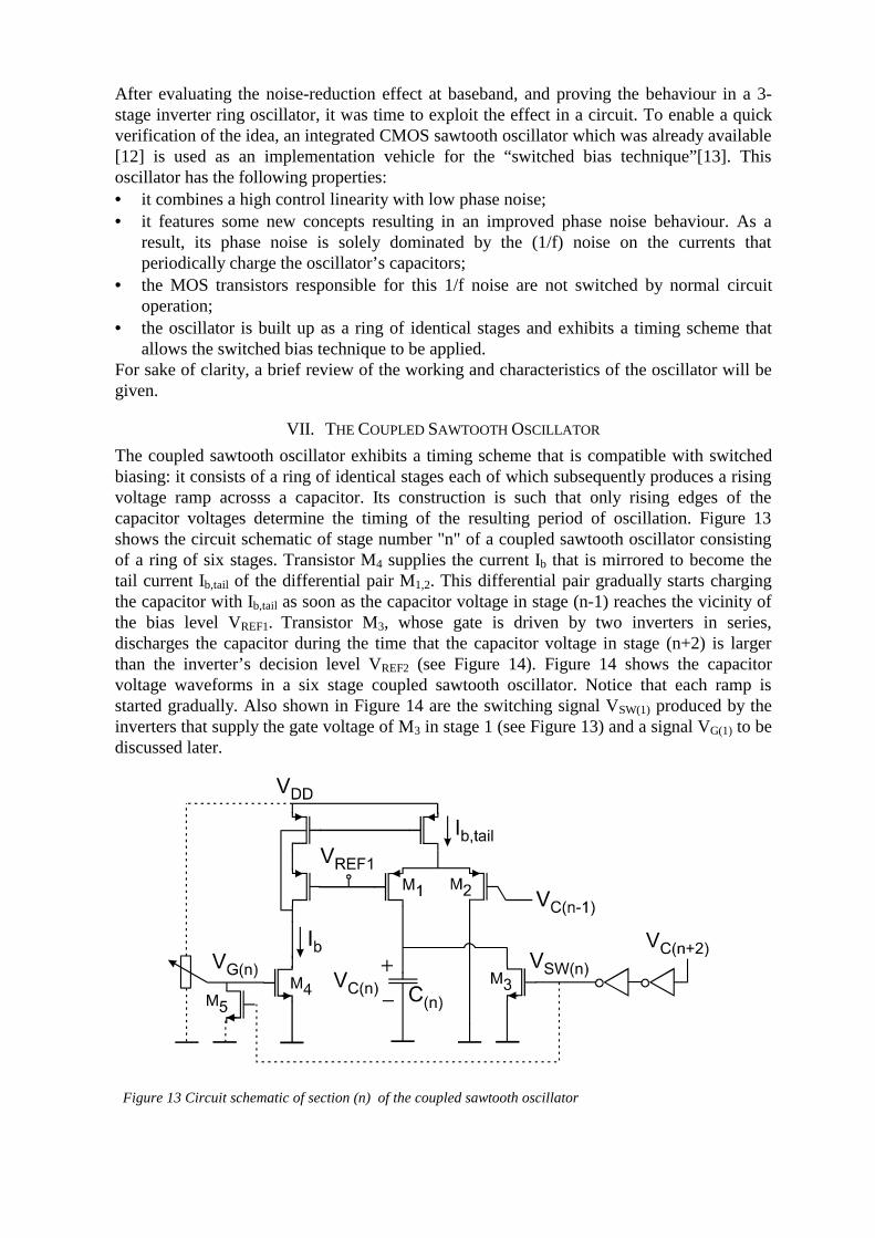
The coupled sawtooth oscillator exhibits a timing scheme that is compatible with switchedbiasing: it consists of a ring of identical stages each of which subsequently produces a risingvoltage ramp acrosss a capacitor. Its construction is such that only rising edges of thecapacitor voltages determine the timing of the resulting period of oscillation. Figure 13shows the circuit schematic of stage number "n" of a coupled sawtooth oscillator consistingof a ring of six stages. Transistor M4 supplies the current Ib that is mirrored to become thetail current Ib,tail of the differential pair M1,2. This differential pair gradually starts chargingthe capacitor with Ib,tail as soon as the capacitor voltage in stage (n-1) reaches the vicinity ofthe bias level VREF1. Transistor M3, whose gate is driven by two inverters in series,discharges the capacitor during the time that the capacitor voltage in stage (n+2) is largerthan the inverter’s decision level VREF2 (see Figure 14). Figure 14 shows the capacitorvoltage waveforms in a six stage coupled sawtooth oscillator. Notice that each ramp isstarted gradually. Also shown in Figure 14 are the switching signal VSW(1) produced by theinverters that supply the gate voltage of M3 in stage 1 (see Figure 13) and a signal VG(1) to bediscussed later.
Figure 13 Circuit schematic of section (n) of the coupled sawtooth oscillator

Figure 14 The capacitor voltage waveforms in the six stage coupled sawtooth oscillator and twoswitching signals Vsw(1) and VG(1) that are used in stage 1 (see Figure 13 with n=1) to respectivelydischarge C1 and accomplish switched biasing.
In [12] the coupled sawtooth oscillator was introduced as a new controlled oscillatorprinciple that allows low phase noise to be achieved in combination with high controllinearity. The phase noise of this type of oscillator issignificantly lower (14dB improvement [12]) than that of a conventional regenerativeoscillator, compared at equal control linearity and power dissipation. This is achieved byusing an alternative for the Schmitt-trigger that is used normally in a regenerative oscillatorto periodically reverse the capacitor current each time the capacitor voltage crosses one ofthe tigger’s two threshold levels. The noise present on these decision levels is the dominantcontributor to phase noise in a conventional regenerative oscillator [11]. This is due to thefast decisions taken by the trigger circuit, resulting in nearly ideal sampling of the threshold-level noise. As a consequence, the threshold-level noise is converted into phase noise over alarge bandwidth.In the coupled sawtooth oscillator the noise, present on the threshold-level VREF1 (see Figure13 and Figure 14), is effectively filtered by the oscillator’s capacitor. This is achieved bygradually turning on the capacitor’s charge current instead of instantly, as happens in theregenerative oscillator. The simple differential pair M1,2 (see Figure 13) performs this task. Itis controlled by the capacitor voltage ramp of the previous stage. When this voltage reachesthe vicinity of VREF1, the differential pair starts to turn on the charge current. During thegradual transition of the differential pair, noise on VREF1 is integrated on the capacitor, thusestablishing an effective filtering. Figure 15 gives a qualitative time-domain impression ofthis filtering. Also shown in this figure is the time error ∆ttrig that would result if a trigger-circuit is used to instantly start a new capacitor voltage ramp. Its variance is much largerthan the variance of the time error ∆tsaw appearing in the sawtooth oscillator, due to theeffective filtering [12].It can be shown [12] that the gradual start-up of the charge current does not introduce anydeterioration of the oscillator’s control-linearity, due to the point-symmetrical transferfunction of the differential pair.

Figure 15 The effective filtering of noise vn on the threshold level VREF1 in the coupled sawtooth oscillatorresults in a smaller time error ∆tsaw compared to the time error ∆ttrig that would appear in a regenerativeoscillator
As a result of the filtering of the threshold-level noise, the (1/f) noise present on thecapacitor’s charge current now becomes the dominant contributor to (1/f induced) phasenoise in the coupled sawtooth oscillator. Thus, in order to further reduce the 1/f inducedphase noise of the coupled sawtooth oscillator using the switched bias technique, it has to beapplied to the transistors that generate the capacitor currents.
As mentioned before, the (1/f) noise present on the capacitor’s charge current Ib,tail (seeFigure 13) dominates the (1/f noise induced) phase noise of the oscillator. Consequently, theswitched-bias technique should be applied to all transistors that contribute 1/f noise to thiscurrent. The oscillator’s operation allows the current Ib,tail, and thus the 1/f noise contributingtransistors, to be switched off when the capacitor in a particular stage is not producing arising ramp. The easiest way to implement this is to switch off these transistors at the sametime when the capacitor is discharged. In this way no change at all will be noticeable in thecapacitor waveforms and the oscillator’s timing is not harmed in any way. The signal,necessary to switch the transistors, is supplied by the oscillator itself.
As there appears no change in the capacitor waveforms, no change in the amount ofupconversion of 1/f noise is expected [8]. As a result, any change in the 1/f noise inducedphase noise when applying the switched bias technique is to be explained by a change in thetransistors’ 1/f noise.
In the experiments described here, an integrated version of the sawtooth oscillator wasused with already available extra bond-outs for capacitors and bias currents. This enables ademonstration of the switched-bias technique. In the IC’s available for experiments, not alltransistors were accessible that contribute 1/f noise to the current Ib,tail. In order todemonstrate the feasibility and the result of the switched bias technique in this oscillator, theswitched-biasing is applied to an external current-bias transistor M4 (see Figure 13) which isavailable on the same die as the oscillator circuit. M4 has a small W/L =4/0.8 such that its 1/fnoise dominates in the current Ib(tail).
The dashed lines in Figure 13 show the implementation of the switched biasing in thecoupled sawtooth oscillator : transistor M5 switches off the bias transistor M4 at the sametime when transistor M3 discharges the capacitor. Figure 14 shows the gate voltage VSW(1) oftransistors M3 and M5 in stage 1 together with the resulting gate voltage VG(1) of biastransistor M4.
Due to experimental limitations, the switched bias technique could be applied only to onestage. In the other stages, low noise current sources are used as bias currents for the PMOScurrent mirrors. The bias current of stage 1 is realized using the before-mentioned transistor

M4 that hence dominates the 1/f noise induced phase noise of the oscillator. This NMOStransistor is used in both constant bias and switched bias mode, for direct comparison.
VIII. EXPERIMENTAL RESULTS OF SWITCHED BIAS IN COUPLED SAWTOOTH OSCILLATOR
In the experiments, the oscillator runs at fosc = 120kHz. Measurements show no effect ofswitched biasing on any of the oscillator’s capacitor-waveforms. However, a large differenceis measured in the phase noise shown in Figure 16: for switched biasing (curve B) the phasenoise at 100Hz carrier-offset frequency is about 8dB lower. In contrast to the basebandresults of Figure 8 no 6 dB correction for duty-cycle effects is necessary here: transistor M4
is switched off during a time interval in which stage 1 is not contributing to the oscillationperiod (and thus to phase noise).
Figure 16 Measured phase noise [dBc/Hz] of the coupled sawtooth oscillator as a function of carrieroffset frequency for the constant bias (curve A) and switched bias condition (curve B): 8 dB reduction at100 Hz.
The experiment shows that switching-off a transistor during phases in which it is not activelycontributing to the circuit's operation, helps to reduce its 1/f noise during active phases. Inaddition, the power consumption in stage 1 is reduced by more than 30%.Although switched-biasing is applied to just one current source in this experimental circuit,it can of course just as well be applied to the other current sources. As all oscillator sectionsare identical and contribute to the phase noise equally, the same reduction in phase noise isexpected in that case.This example of applying the switched bias technique in an existing sawtooth oscillatorillustrates the power of this technique. It reduces the 1/f induced phase noise as well as thepower consumption of the oscillator. While normally lower phase noise is achieved in acircuit by burning more power.
IX. CONCLUSIONS
The intrinsic 1/f noise of MOS transistors is shown to decrease by periodically switching atransistor from an operational state in strong inversion to a rest state close to accumulation(switched bias technique). It has been shown that this physical effect has a significant effecton the phase noise of CMOS ring oscillator (Phase Noise reduction of 8dB). “SwitchedBiasing” has been proposed as a circuit technique that exploits intentional on-off switchingof MOS transistors with the purpose to reduce their intrinsic 1/f noise. The technique wasimplemented in a 6-stage coupled sawtooth oscillator [12] running at fosc = 120 kHz.Experiments show that the switched bias technique can be used with benefit: it not only
results in a 30% reduction of power consumption but also in a 8dB reduction of the 1/f noiseinduced phase noise. As a means to reduce 1/f noise, the authors believe that the switched-bias technique can be made applicable in many other circuits where 1/f noise is of concern.
X. AKNOWLEDGEMENTS
Several people have contributed to the succes of this project and are kindly acknowledgedfor their contributions: G. Hoogzaad, A.P. v.d. Wel, A.J.M. v. Tuijl, R.F. Wassenaar, HWallinga and A. Sempel. Part of this work has been sponsored by Philips ResearchLaboratories, Eindhoven.
XI. REFERENCES
[1] M. S. Keshner, “1/f Noise”, Proceedings of the IEEE, Vol. 70, No. 3, pp. 212-218, March 1982.[2] I. Bloom, Y. Nemirovsky, “1/f Noise Reduction of Metal-Oxide-Semiconductor Transistors by cycling from inversion
to accumulation”, Applied Physics Letters, Vol. 58 (15), pp. 1664-1666, 15 April 1991.[3] B. Dierickx, E. Simoen, “The Decrease of “Random Telegraph Signal” Noise in Metal-Oxide-Semiconductor Field-
Effect Transistors when cycled from inversion to accumulation”, Journal of Applied Physics, Vol. 71 (4), 2028-2029,15 February 1992.
[4] A. P. van der Wel, S. L. J. Gierkink, E. A. M. Klumperink, H. Wallinga, R. F. Wassenaar, “Discussiestuk: 1/f ruis in degeschakelde toestand: nuttig, interessant of beide?", Tijdschrift van het Nederlands Elektronica- en Radiogenootschap,deel 63, nr. 1, pp. 14-22, 1998.
[5] A. P. van der Wel, E. A. M. Klumperink, S. L. J. Gierkink, R. F. Wassenaar, H. Wallinga, “MOSFET 1/f noisemeasurement under switched bias conditions”, Submitted to IEEE Electron Device Letters.
[6] B. Razavi, “A Study of Phase Noise in CMOS Oscillators”, IEEE Journal of Solid-State Circuits, Vol. 31, No. 3, pp.331-343, March 1996.
[7] S. L. J. Gierkink, A. v. d. Wel, G. Hoogzaad, E. A. M. Klumperink, A. J. M. v. Tuijl, “Reduction of the 1/f NoiseInduced Phase Noise in a CMOS Ring Oscillator by Increasing the Amplitude of Oscillation”, The 1998 InternationalSymposium on Circuits and Systems, May 31-June 3, Monterey, USA, CD-ROM Paper MPA9-8, 1998.
[8] A. Hajimiri, T. H. Lee, "A General Theory of Phase Noise in Electrical Oscillators", IEEE Journal of Solid-StateCircuits, vol. 33, No. 2, 179-194, February 1998.
[9] S. L. J. Gierkink, E. A. M. Klumperink, T. J. Ikkink, A. J. M. v. Tuijl, “Reduction of Intrinsic 1/f Device Noise in aCMOS Ring Oscillator”, Proceedings of the 24th European Solid-State Circuits Conference, pp. 272-275, The Hague,The Netherlands, 22-24 September 1998.
[10] S.L.J. Gierkink, E.A.M. Klumperink, A.P. van der Wel, G. Hoogzaad, A.J.M. van Tuijl, B. Nauta, “Intrinsic 1/fDevice Noise Reduction and its Effect on Phase Noise in CMOS Ring Oscillators IEEE Journal of Solid-StateCircuits., July 1999.
[11] A.A. Abidi and R.G. Meyer, "Noise in Relaxation Oscillators”, IEEE Journal of Solid-State Circuits, vol. 18, No. 6,794-802, December 1983.
[12] S.L.J. Gierkink, A.J.M. van Tuijl, “A Coupled Sawtooth Oscillator combining Low Jitter and High Control Linearity”,Proceedings of the 24th European Solid-State Circuits Conference, pp. 96-99, The Hague, The Netherlands, 22-24September 1998.
[13] S.L.J. Gierkink, Eric. A. M. Klumperink, A.J.M. van Tuijl, B. Nauta, “Reducing 1/f Noise and power consumption bythe “switched Bias Technique, Proceedings of the 25th European Solid-State Circuits Conference, Duisburg, Germany,21-23 September 1999