registers and counters - courses.muscedere.comcourses.muscedere.com/8821701/88-217-ch6.pdfto form a...
TRANSCRIPT

©2018 Roberto Muscedere 1Images ©2013 Pearson Education Inc.
Registers and CountersRegisters and Counters
• A register is a group of flip-flops which share a common clock
• An n-bit register consists of a group of n flip-flops capable of storing n bits of binary information• May have combinational gates that perform certain data-
processing tasks
• A counter is essentially a register that goes through a predetermined sequence of binary states• Gates in the counter are connected in such a way as to
produce the prescribed sequence of states

©2018 Roberto Muscedere 2Images ©2013 Pearson Education Inc.
Basic RegisterBasic Registerss• Various types of registers are
available commercially• Simplest register is one that
consists of only flip-flops, without any gates
• Figure shows a register constructed with four D flip-flops to form a four-bit data storage register• Common clock input triggers all
flip-flops on the positive edge of each pulse
• Binary data at the 4-bit inputs (I) are transferred into the register after the clock edge and are available at the output (A)
• Active-low reset (Clear) sets all registers to zero asynchronously

©2018 Roberto Muscedere 3Images ©2013 Pearson Education Inc.
Parallel Load RegisterParallel Load Registerss• Useful to have a condition as to
when to load a register with data• Figure shows a 4-bit parallel load
register with a Load or Enable• “Load” input determines the action to be
taken with each clock pulse• When 1, the data at the inputs (I) are
transferred into the register with the next positive edge of the clock
• When 0, the outputs of the flip-flops are connected to their respective inputs and loaded back into the register at the next positive clock edge
• Preferred method since the clock is not gated (which could cause synchronization issues)

©2018 Roberto Muscedere 4Images ©2013 Pearson Education Inc.
Parallel Load Register HDLParallel Load Register HDL• Can use “if” or “case” to
infer a MUX before the flip-flop
• Depending on synthesizer and cells available, you may be able to exclude the “else” or default condition and it will use a flip-flop with enable option
// Verilog-2001module pl_reg (output reg[3:0] A, input CK, Load,input [3:0] I);
always @(posedge CK)beginif (Load) A <= I;else A <= A;
// or:
case (Load)0: A <= A;1: A <= I;
endcaseend
endmodule

©2018 Roberto Muscedere 5Images ©2013 Pearson Education Inc.
Shift RegisterShift Register• A shift register is capable of shifting the binary information
held in each cell to its neighboring cell, in a selected direction• Consists of a chain of flip-flops in cascade, with the output of one
flip-flop connected to the input of the next flip-flop• All flip-flops receive the same clock
• Figure shows a simple shift register which can only shift right (unidirectional)

©2018 Roberto Muscedere 6Images ©2013 Pearson Education Inc.
Shift RegisterShift Register• When enabled (Enable=1), the shift register moves data
from D0 to serial out (SO), D1 to D0, D2 to D1, D3 to D2, and serial in (SI) to D3
• When disabled (Enable=0), output from each flip-flop cycles back to input
• We always assume flip-flop setup and hold times are not violated
• (Warning: The text book shows unfavorable designs, ie. gated clocks, and elects later to correct them)

©2018 Roberto Muscedere 7Images ©2013 Pearson Education Inc.
Parallel Load Shift Register HDLParallel Load Shift Register HDL• Use concatenation and
bit ranges to implement shift registers:
{SI,D[3:1]} is the same as{SI,D[3],D[2],D[1]}
// Verilog-2001module pl_sreg (output reg SO,input CK, Enable, SI);
reg [3:0] D;
always @(posedge CK)beginSO <= D[0];if (Enable)
D <= {SI,D[3:1]};else D <= D;
end
endmodule

©2018 Roberto Muscedere 8Images ©2013 Pearson Education Inc.
Generic Parallel LoadGeneric Parallel LoadShift Register HDLShift Register HDL
• Can use “parameters” to make code “generic” to any configuration• Should use before defining I/O
bit widths
• Instantiate module later with different parameters (example):
pl_sreg #(4) U0 (SO,CK,Enable,SI);
pl_sreg #(8) U1 (SO2,CK,Enable,SO);
// Verilog-95module pl_sreg (SO, CK, Enable,SI);
parameter n = 4;
output SO;input CK, Enable, SI;reg SO;reg [n-1:0] D;
always @(posedge CK)beginSO <= D[0];if (Enable)
D <= {SI,D[n-1:1]};else D <= D;
end
endmodule

©2018 Roberto Muscedere 9Images ©2013 Pearson Education Inc.
Serial TransferSerial Transfer• The datapath of a digital system is said to operate
in serial mode when information is transferred and manipulated one bit at a time
• In contrast to parallel transfer, whereby all the bits of the register are transferred at the same time
• Most operations are performed in parallel because it is a faster whereas serial operations are slower because a datapath operation takes several clock cycles
• Serial operations have the advantage of requiring fewer hardware components and in some cases can operate at higher clocks speed than parallel operations

©2018 Roberto Muscedere 10Images ©2013 Pearson Education Inc.
Serial TransferSerial Transfer• Serial transfer of information from register A to register B is
done with shift registers• To avoid reloading of register A, its output is fed back to its input for
this example• As the clock pulses, the initial contents of register B are shifted out
through its serial output (may be transferred to a third shift register)• The “Enable” and “Clock” determine when the shift happens• After 4 enabled pulses, register A is back to it’s initial value and
register B has the contents of register A

©2018 Roberto Muscedere 11Images ©2013 Pearson Education Inc.
Serial AdderSerial Adder• Parallel adder shown adds number
by using cascading full adders• For a serial implementation, one bit
of each inputs A, B, and C are shifted in, starting at the LSB, processed by the full adder, and the results S and C are stored
• One possibility is to save the sum (S) back into A to accumulate future results over time
• Only the previous carry (C) needs to be remembered

©2018 Roberto Muscedere 12Images ©2013 Pearson Education Inc.
Serial AdderSerial AdderExample: Add 6 + 7• Serial adder stores result in
augend; it is accumulated• C0 is initially 0 (cycle 0)• Sum is stored in Augend
MSB every cycle• Addend MSB gets new
Addend every cycle• Carry register stores only the
current carry• Add more numbers by
shifting in via Serial Input (SI) on addend
• Additional control required to coordinate resets

©2018 Roberto Muscedere 13Images ©2013 Pearson Education Inc.
Serial Adder: Alternate DesignSerial Adder: Alternate Design• Uses separate shift registers for input and output• Still requires only one FA

©2018 Roberto Muscedere 14Images ©2013 Pearson Education Inc.
Universal Shift Register (USR)Universal Shift Register (USR)• Use larger MUX to
allow for more options
Depending on “Mode”, USR can:
• 00: Preserve previous A • 01: Shift right (MSB
serial in, A[0] serial out)• 10: Shift left (LSB serial
in, A[3] serial out)• 11: Load in a parallel
value from I

©2018 Roberto Muscedere 15Images ©2013 Pearson Education Inc.
Generic Universal Shift Register HDLGeneric Universal Shift Register HDL
• For Verilog 2001+, parameters must be declared before ports
• Clear is active high
// Verilog-2001module univ_sreg #(parameter n=4)(output reg [n-1:0] A, input CK,Clear, MSB, LSB, input [1:0] Mode,input [n-1:0] I);
always @(posedge CK,posedge Clear)
beginif (Clear) A <= 0;else begin
case (Mode)0: A <= A;1: A <= {MSB,A[n-1:1]};2: A <= {A[n-2:0],LSB};default: A <= I;
endcaseend
endendmodule

©2018 Roberto Muscedere 16Images ©2013 Pearson Education Inc.
Synchronous CountersSynchronous Counters
• Skipping Ripple Counters (Section 6.3)• Uses gated clocks• Domino triggers• Creates bad habits; avoid them
• Focus on Synchronous counters• All flip-flops use the same clock• Similar to creating state machine circuits from
state tables (chapter 5)• Only present state influences next state

©2018 Roberto Muscedere 17Images ©2013 Pearson Education Inc.
Binary Up CounterBinary Up Counter• Simple design• Can do by
inspection or by using state tables
• Use T flip-flops• Can use others,
but T is often easier for counters
• XOR preceding D flip-flop
A 3 A 2 A 1 A 0 A 3 A 2 A 1 A 0 T A 3 T A 2 T A 1 T A 0
0 0 0 0 0 0 0 1 0 0 0 10 0 0 1 0 0 1 0 0 0 1 10 0 1 0 0 0 1 1 0 0 0 10 0 1 1 0 1 0 0 0 1 1 10 1 0 0 0 1 0 1 0 0 0 10 1 0 1 0 1 1 0 0 0 1 10 1 1 0 0 1 1 1 0 0 0 10 1 1 1 1 0 0 0 1 1 1 11 0 0 0 1 0 0 1 0 0 0 11 0 0 1 1 0 1 0 0 0 1 11 0 1 0 1 0 1 1 0 0 0 11 0 1 1 1 1 0 0 0 1 1 11 1 0 0 1 1 0 1 0 0 0 11 1 0 1 1 1 1 0 0 0 1 11 1 1 0 1 1 1 1 0 0 0 11 1 1 1 0 0 0 0 1 1 1 1
Present State Next State Flip-Flop Inputs

©2018 Roberto Muscedere 18Images ©2013 Pearson Education Inc.
Binary Up CounterBinary Up Counter• Flip-Flop inputs:
TA0 = 1TA1 = A0
TA2 = A1A0
TA3 = A2A1A0
= A2 TA2
• Scales up easily• TA0 can be the
enable signal

©2018 Roberto Muscedere 19Images ©2013 Pearson Education Inc.
Binary Down CounterBinary Down Counter• Simple design• Can do by
inspection or by using state tables
• Will use T flip-flops again
A 3 A 2 A 1 A 0 A 3 A 2 A 1 A 0 T A 3 T A 2 T A 1 T A 0
0 0 0 0 1 1 1 1 1 1 1 10 0 0 1 0 0 0 0 0 0 0 10 0 1 0 0 0 0 1 0 0 1 10 0 1 1 0 0 1 0 0 0 0 10 1 0 0 0 0 1 1 0 1 1 10 1 0 1 0 1 0 0 0 0 0 10 1 1 0 0 1 0 1 0 0 1 10 1 1 1 0 1 1 0 0 0 0 11 0 0 0 0 1 1 1 1 1 1 11 0 0 1 1 0 0 0 0 0 0 11 0 1 0 1 0 0 1 0 0 1 11 0 1 1 1 0 1 0 0 0 0 11 1 0 0 1 0 1 1 0 1 1 11 1 0 1 1 1 0 0 0 0 0 11 1 1 0 1 1 0 1 0 0 1 11 1 1 1 1 1 1 0 0 0 0 1
Present State Next State Flip-Flop Inputs

©2018 Roberto Muscedere 20Images ©2013 Pearson Education Inc.
Binary Down CounterBinary Down Counter• Flip-Flop inputs:
TA0 = 1TA1 = A0'TA2 = A1'A0'TA3 = A2'A1'A0'
= A2'TA2
• Scales up easily• TA0 can be the
enable signal
©2018 Roberto Muscedere 21Images ©2013 Pearson Education Inc.
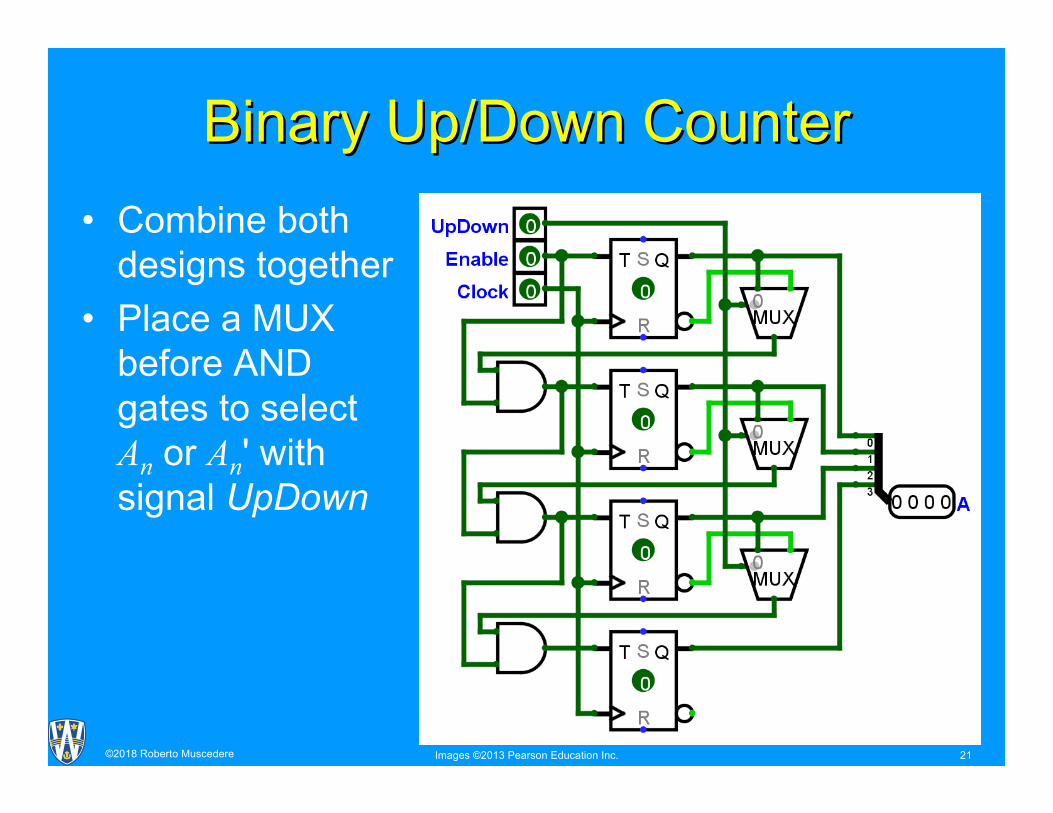
Binary Up/Down CounterBinary Up/Down Counter• Combine both
designs together• Place a MUX
before AND gates to select An or An' with signal UpDown

©2018 Roberto Muscedere 22Images ©2013 Pearson Education Inc.
BCD CounterBCD CounterOutput
A 3 A 2 A 1 A 0 A 3 A 2 A 1 A 0 y T A 3 T A 2 T A 1 T A 0
0 0 0 0 0 0 0 1 0 0 0 0 10 0 0 1 0 0 1 0 0 0 0 1 10 0 1 0 0 0 1 1 0 0 0 0 10 0 1 1 0 1 0 0 0 0 1 1 10 1 0 0 0 1 0 1 0 0 0 0 10 1 0 1 0 1 1 0 0 0 0 1 10 1 1 0 0 1 1 1 0 0 0 0 10 1 1 1 1 0 0 0 0 1 1 1 11 0 0 0 1 0 0 1 0 0 0 0 11 0 0 1 0 0 0 0 1 1 0 0 1
Present State Next State Flip-Flop Inputs
• Output y used to trigger next digit

©2018 Roberto Muscedere 23Images ©2013 Pearson Education Inc.
BCD CounterBCD Counter• Use state table
with T flip-flopsTA0 = 1TA1 = A3'A0
TA2 = A1A0
TA3 = A3A0 +A2A1A0
y = A3A0

©2018 Roberto Muscedere 24Images ©2013 Pearson Education Inc.
Binary Up/Down Counter with LoadBinary Up/Down Counter with Load

©2018 Roberto Muscedere 25Images ©2013 Pearson Education Inc.
Generic Binary Up/Down Counter Generic Binary Up/Down Counter (with Load) HDL(with Load) HDL
• Use “if” to avoid considering all cases since there are multiple inputs (UpDown, Enable, Load) instead of one (ie. Mode from previous example)
• Only need begin/end with more than a single statement• If/elses are chained
// Verilog-2001module binupdownload#(parameter n=4)(output reg[n-1:0] A, input CK, Clear,UpDown, Enable, Load, input[n-1:0] I);
always @(posedge CK,posedge Clear)
beginif (Clear) A <= 0;else if (Enable)
if (Load) A <= I;else if (UpDown)A <= A - 1;
elseA <= A + 1;
endendmodule

©2018 Roberto Muscedere 26Images ©2013 Pearson Education Inc.
BCD Up/Down Counter fromBCD Up/Down Counter fromBinary Up/Down Counter with LoadBinary Up/Down Counter with Load
• Use binary counter with load to reset BCD to 0 or 9 based on up/down respectively
• Load value is set based on up/down

©2018 Roberto Muscedere 27Images ©2013 Pearson Education Inc.
Counter with Unused StatesCounter with Unused States• Counter with n flip-flops has at most 2n
states• Unused states handled with X’s may not
move onto valid states if entered; determined after implementation
• Example: State table implements a gateless design with unused states 011 and 111, but they recover to known statesJA = BKA = BJB = CKB = 1JC = B'KC = 1

©2018 Roberto Muscedere 28Images ©2013 Pearson Education Inc.
Ring CounterRing Counter• Uses circular shift register with only one flip-flop set at a
time (one flip-flop per state)• The “1” is shifted from one flip-flop to the next on each clock• Reset signal asserts Set/Resets of flip-flops to create initial
state• Could also use a 2-bit counter which drives a 2-to-4 decoder
to achieve a similar result• Uses less flip-flops, but decoder size can dominate for large number
of states

©2018 Roberto Muscedere 29Images ©2013 Pearson Education Inc.
Ring Counter HDLRing Counter HDL• Use concatenation and
bit ranges to implement shift registers
// Verilog-2001module ringcounter #(parametern=4) (output reg [n-1:0] T,input CK, Reset);
always @(posedge CK, posedge Reset)
beginif (Reset) begin
T[n-1:1] <= 0; T[0] <= 1;endelsebegin
T <= {T[n-2:0],T[n-1]};end
end
endmodule

©2018 Roberto Muscedere 30Images ©2013 Pearson Education Inc.
Johnson CounterJohnson Counter• Modified ring counter with
complement of last flip-flop fed-back instead
• Generates 2n states from nflip-flops
• 2n AND 2-input gates required to decode state (Sx)• Examine adjacent patterns
only
• If in unpredictable state, it will not reset on its own• Fix: DC = (A + C)B

©2018 Roberto Muscedere 31Images ©2013 Pearson Education Inc.
Johnson Counter HDLJohnson Counter HDL• Use generic model
where n is the number of flip-flops; 2n outputs
• Calculate “S” with “for” loop• Infers parallelism• Use “integer” type for
control variable• Loop limit must be
known at compile time
• Can’t use “i++”; use “i=i+1”
// Verilog-2001module johnsoncounter #(parameter n=4)(output [n*2-1:0] S, input CK, Reset);
reg [n-1:0] T;integer i;always @(posedge CK, posedge Reset)if (Reset) T <= 0;else T <= {T[n-2:0],~T[n-1]};
always @(T)beginS[0] = ~T[0] & ~T[n-1];S[n] = T[0] & T[n-1];for (i=0;i<n-1;i=i+1)begin
S[i+1] = T[i] & ~T[i+1];S[n+i+1] = ~T[i] & T[i+1];
endendendmodule