regulator power module - we-online.com · regulator module) vfamily, are step-down or “buck”...
TRANSCRIPT

ANS006b, 2016-02-25, RaB Page 1 of 18
A P P L I C A T I O N N O T E
Selecting and Designing with MagI3C Power Modules
ANS006B BY RANJITH BRAMANPALLI
Table of Contents _______________________________________________
Introduction
Standard Features
Probing the Switch Node
Selecting the Right MagI³C Module for the Job
Design Considerations
PCB Layout
Thermal Recommendations
1. Introduction ________________________________________________
MagI³C Power Modules (Magnetic Integrated Intelligent IC) from Würth Elektronik eiSos afford the system
designer a highly integrated switching power supply with high power density, very low external component
count and excellent electromagnetic compatibility (EMC) characteristics. The VDRM (Variable Step Down
Regulator Module) family, are step-down or “buck” regulators that contain the control circuitry, power
MOSFETs, the output inductor and several discrete resistors and capacitors within a molded package and a
metal substrate. The packaging is based on the industry standard TO-263 and reflects the concept of using
these modules as if they were linear regulators. By following the selection and simple design procedures
outlined in the application note, the user can employ a MagI³C Power Module and be assured that it will work
as easily as a linear regulator, but with much higher efficiency.
COUT
LSS
HSS
RON
VIN
EN PGND
SSFB
VOUT
10µH
CVCC CBOOST
0.47µF
Power Module
AGND
Controller/
Power Control/
Protection Circuitry
Linear
Regulator
1
2
6
CSS
5
3 EP4
7
CINCFF
VIN
UVLO
VIN VOUT
AGNDAGND
RON RFBT
RFBB

ANS006b, 2016-02-25, RaB Page 2 of 18
A P P L I C A T I O N N O T E
Selecting and Designing with MagI3C Power Modules
Figure 1: Internal view and external view of a VDRM series MagI³C power module
Figure 2: External component comparison of a MagI³C power module and a standard LDO
1.1. Standard Features
MagI³C Power Modules include the following features common to many switching regulators:
Low Power Shutdown / Undervoltage Lockout
When the enable pin (EN) is forced to a logic low, the module is disabled, and drawing a minimal current from
the VIN rail. The EN pin can also be used as a precision threshold for undervoltage lockout by connecting a
resistor divider between VIN and AGND. This is shown using resistors RENT and RENB in Figure 2.
CIN
RON
VIN
EN PGND SS
FB
VOUT
Module
CSS
CFF
COUT
AGND
1
2
3
EP 5
4
6
7VIN VOUT
RENB
RENT
RON RFBT
RFBB
IN OUT
IMON
TEMP
ILIM
SET
VIN VOUT
36V, 1A LDO

ANS006b, 2016-02-25, RaB Page 3 of 18
A P P L I C A T I O N N O T E
Selecting and Designing with MagI3C Power Modules
Soft Start
The soft start feature prevents large inrush currents from being drawn from the VIN rail by controlling the slew
rate of the rising output voltage when the module is enabled. The larger the capacitor at the soft start (SS) pin,
the longer it takes for VOUT to reach its target value, and hence the lower the peak inrush current.
Emulated Discontinuous Conduction Mode
When output current is approximately 450 mA or below the MagI³C Power Modules turn off the low side,
synchronous MOSFET, emulating the function of a diode. This prevents current from flowing from the VOUT
pin to ground. Due to this emulated discontinuous conduction mode (DCM), the modules cannot sink current
at their outputs. The principal advantage of emulated DCM is during pre-biased startup, a condition that often
occurs when several power supplies all connect to the same load, such as a microprocessor or FPGA. Parasitic
diodes present inside the digital device can allow voltage to leak from an active power supply onto the output
of a disabled power supply, precharging the output capacitor. Emulated DCM prevents problems with
transients or high peak currents upon enabling the pre-biased supply.
2. Probing the Switch Node ______________________________________
The switching node is the electrical net that connects the two power switches to the inductive component in a
switching power supply. Probing this node with an oscilloscope is the first step in testing for proper operation,
but it is not accessible in MagI³C Power Modules. The following two techniques can be used to test the
switching action:
2.1. Radiated Voltage Using a Voltage Probe
This method is fairly simple, as shown in Figure 3. Simply remove the spring tip and the ground lead from a
standard oscilloscope voltage probe, and hold the tip directly above the body of the module. The probe will
pick up the electromagnetic field radiating from the switching node.
Figure 3: Testing the switching node via voltage probes and the radiated EM field.
WPMDH1302401JT EVB, VIN = 24 V, VOUT = 12 V, IOUT = 2 A

ANS006b, 2016-02-25, RaB Page 4 of 18
A P P L I C A T I O N N O T E
Selecting and Designing with MagI3C Power Modules
2.2. Inductor Current Using a Current Probe
This method is more invasive, but has the advantage of showing the inductor current. A stable square wave
voltage at the switching node indicates that a switching converter is operating properly, but a stable triangle
wave current through the inductor is just as valid. In order to perform this test the VOUT pin of the module must
be de-soldered, lifted, and a loop of wire placed in series as shown in Figure 4.
Figure 4: Testing the switching node via current probe in series with the output.
WPMDH1302401JT EVB, VIN = 24 V, VOUT = 12 V, IOUT = 3 A
3. Selecting the Right MagI³C Module for the Job ___________________
3.1. Product Famil ies
VDRM Family Part Description
Article Number
VIN [V] VOUT [V] IOUT,max [A] fSW [kHz]
WPMDH1200601JT 171 020 601 6 to 42 0.8 to 6.0 2.0 200 to 800
WPMDM15006021JT 171 050 601 6 to 36 0.8 to 6.0 5.0 650 to 950
WPMDH1102401JT 171 012 401 6 to 42 5.0 to 24.0 1.0 200 to 800
WPMDH1152401JT 171 012 402 6 to 42 5.0 to 24.0 1.5 200 to 800
WPMDH1302401JT 171 032 401 6 to 42 5.0 to 24.0 3.0 200 to 800
Table 1: The TO263 package VDRM family of MagI³C Power Modules
3.2. Two Protection Features: Current Limit and Thermal Shutdown
The MagI³C families feature both peak output current limit and thermal shutdown. The current limit circuits
have a threshold above the maximum output currents listed in Table 1. However, it is important to keep in mind
that thermal shutdown takes precedence over the current limit. Thermal shutdown engages at a typical junction
temperature of 165 ºC. A restart after thermal shutdown is automatic, with a typical hysteresis of 15 ºC. In
practice the thermal shutdown is likely to engage before the peak current limit when the MagI³C devices are
operated near their maximum output voltage and maximum output current. Section 6, Thermal Considerations,
gives details on the thermal analysis that should be part of every design cycle when using power modules, and

ANS006b, 2016-02-25, RaB Page 5 of 18
A P P L I C A T I O N N O T E
Selecting and Designing with MagI3C Power Modules
this will help the user ensure that their MagI³C module can deliver all the power required without running into
either current limit or thermal shutdown.
3.3. Avoid Oversizing the Current Limit
Selecting the right module based on output current and output voltage is very straightforward by looking at the
possibilities in Table 1. For example, for an output of 12 V at a maximum of 1.2 A, the WPMDH1152401JT
would be the best choice. For an output of 3.3 V at a maximum of 4 A, the WPMDM1500602JT would be the
correct choice. System designers might be tempted to oversize their module choice in terms of current to
reduce the power dissipation and temperature rise, but there are two good reasons to avoid this. First, the
internal inductor values have been chosen carefully to give proper ratios of peak-to-peak ripple current to
average current based upon the maximum output current. Second, the higher current modules use larger
MOSFETs, and at low output current their higher gate charge and longer switching times will cancel out any
efficiency improvements coming from their lower RDSON. This balance of losses is reflected in the power
efficiency versus output current curves in each MagI³C Power Module datasheet, which reaches a peak in the
middle third of each curve. Therefore, it is always best to select the module whose maximum output current is
just above the highest output current for the given application.
Figure 5: Efficiency plots show that higher current MagI³C power modules
do not improve efficiency at low output current
50
60
70
80
90
100
0.05 0.1 0.2 0.4 0.6 0.8 1
Po
we
r E
ffic
ien
cy [
%]
Output Current [A]
VIN = 12 V (DC) VO = 5 V (DC)
WPMDH1200601JT (1A)
WPMDM15006021JT (5A)
50
60
70
80
90
100
0.05 0.1 0.2 0.4 0.6 0.8 1
Po
wer
Eff
icie
ncy [
%]
Output Current [A]
VIN = 24 V (DC) VO = 5 V (DC)
WPMDH1200601JT (1A)
WPMDM15006021JT (5A)
ANS006b, 2016-02-25, RaB Page 6 of 18
A P P L I C A T I O N N O T E
Selecting and Designing with MagI3C Power Modules
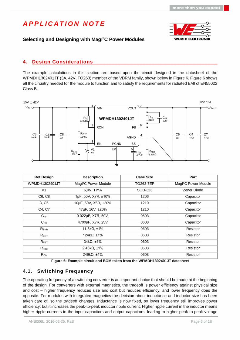
4. Design Considerations _______________________________________
The example calculations in this section are based upon the circuit designed in the datasheet of the
WPMDH1302401JT (3A, 42V, TO263) member of the VDRM family, shown below in Figure 6. Figure 6 shows
all the circuitry needed for the module to function and to satisfy the requirements for radiated EMI of EN55022
Class B.
Ref Design Description Case Size Part
WPMDH1302401JT MagI³C Power Module TO263-7EP MagI³C Power Module
V1 6,0V, 1 mA SOD-323 Zener Diode
C6, C8 1μF, 50V, X7R, ±10% 1206 Capacitor
3, C5 10µF, 50V, X5R, ±20% 1210 Capacitor
C4, C7 47µF, 16V, ±20% 1210 Capacitor
CFF 0.022μF, X7R, 50V, 0603 Capacitor
CSS 4700pF, X7R, 25V 0603 Capacitor
RENB 11,8kΩ, ±1% 0603 Resistor
RENT 124kΩ, ±1% 0603 Resistor
RFBT 34kΩ, ±1% 0603 Resistor
RFBB 2.43kΩ, ±1% 0603 Resistor
RON 249kΩ, ±1% 0603 Resistor
Figure 6: Example circuit and BOM taken from the WPMDH1302401JT datasheet
4.1. Switching Frequency
The operating frequency of a switching converter is an important choice that should be made at the beginning
of the design. For converters with external magnetics, the tradeoff is power efficiency against physical size
and cost – higher frequency reduces size and cost but reduces efficiency, and lower frequency does the
opposite. For modules with integrated magnetics the decision about inductance and inductor size has been
taken care of, so the tradeoff changes. Inductance is now fixed, so lower frequency still improves power
efficiency, but it increases the peak-to-peak inductor ripple current. Higher ripple current in the inductor means
higher ripple currents in the input capacitors and output capacitors, leading to higher peak-to-peak voltage
4.7nF
RFBB
2.43kΩ
RFBT
34kΩ
C8
RON
VIN
EN PGND SS
FB
VOUT
WPMDH1302401JT
CSS
CFF
C6AGND
1
2
3
EP 5
4
6
7
C4
22nF
1µF 47µF
RENB
118kΩ
RENT
124kΩ 1µF
C310µF
R1
249kΩ
12V / 3A15V to 42V
VIN VOUT
C510µF
C747µF
V16V

ANS006b, 2016-02-25, RaB Page 7 of 18
A P P L I C A T I O N N O T E
Selecting and Designing with MagI3C Power Modules
ripple at the input and the output of the power supply and higher RMS currents in the input and output
capacitors. Therefore switching frequency cannot be made arbitrarily low or high, but continues to be a
compromise. The VDRM series MagI³C modules define a range of user-programmable frequencies in the
electrical characteristics table of their datasheets because power dissipation will change greatly with the output
voltage. Higher output voltage means higher output power and hence higher power dissipation in the module.
The higher the expected power dissipation in the module, the lower the switching frequency should be.
4.2. L-C Input Filter with Damping
Buck converters draw a discontinuous current from the input source. Even with good quality input capacitors
to supply the buck regulator inherent AC current, the source will supply some current at AC, and the result is
conducted electromagnetic interference (EMI) on the input lines. The longer the leads, PCB traces and wiring
harnesses that connect these high ripple DC-DC converters to their input sources, the more likely that this
conducted EMI also becomes radiated EMI owing to the unwanted antenna behavior of the leads. An input L-
C filter placed close to the DC-DC converter is a good way to reduce conducted EMI, and by filtering before
the noise can “contaminate” the input leads radiated EMI is reduced as well.
Not every laboratory has access to dedicated equipment for measuring and testing conducted EMI, let
alone the special antennas and anechoic chambers needed for radiated EMI. The following procedure is based
upon correlation of time-domain current waveforms that can be predicted and measured with a common
oscilloscope to the differential-mode conducted noise in the frequency domain.
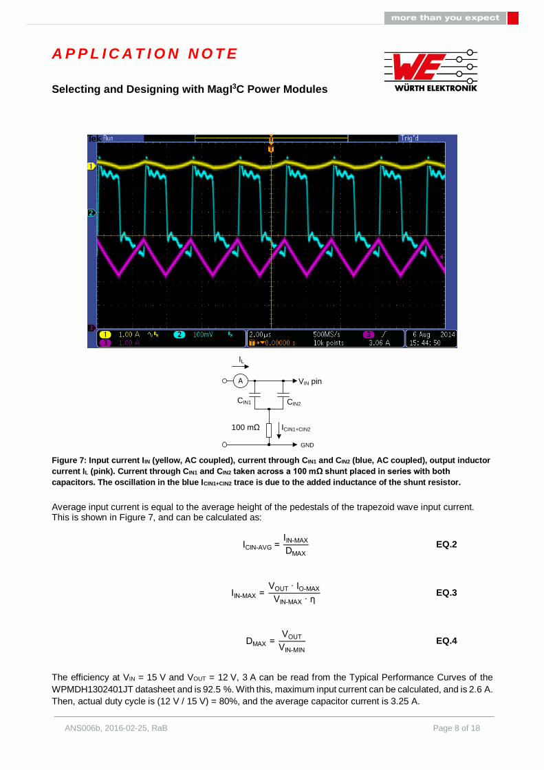
Estimating Noise Amplitude
The following equation can be used to estimate the amplitude of the first harmonic of the differential mode
conducted noise based upon the input current waveform:
A1st = 20 · log (
ICIN-AVG
π2 · CIN · fSW sin (π · Dmax)
1µV) EQ.1
Figure 7 shows the input current from the source and also the ripple current through the input capacitors during
maximum load and minimum input voltage – the worst-case for EMI.
ANS006b, 2016-02-25, RaB Page 8 of 18
A P P L I C A T I O N N O T E
Selecting and Designing with MagI3C Power Modules
Figure 7: Input current IIN (yellow, AC coupled), current through CIN1 and CIN2 (blue, AC coupled), output inductor
current IL (pink). Current through CIN1 and CIN2 taken across a 100 mΩ shunt placed in series with both
capacitors. The oscillation in the blue ICIN1+CIN2 trace is due to the added inductance of the shunt resistor.
Average input current is equal to the average height of the pedestals of the trapezoid wave input current. This is shown in Figure 7, and can be calculated as:
ICIN-AVG = IIN-MAX
DMAX
EQ.2
IIN-MAX = VOUT · IO-MAX
VIN-MAX · η EQ.3
DMAX = VOUT
VIN-MIN
EQ.4
The efficiency at VIN = 15 V and VOUT = 12 V, 3 A can be read from the Typical Performance Curves of the
WPMDH1302401JT datasheet and is 92.5 %. With this, maximum input current can be calculated, and is 2.6 A.
Then, actual duty cycle is (12 V / 15 V) = 80%, and the average capacitor current is 3.25 A.
A VIN pin
GND
IL
100 mΩ ICIN1+CIN2
CIN1 CIN2

ANS006b, 2016-02-25, RaB Page 9 of 18
A P P L I C A T I O N N O T E
Selecting and Designing with MagI3C Power Modules
Before the noise voltage of the first harmonic can be estimated, one important characteristic of MLC capacitors
has to be taken into account – their capacitance loss due to DC bias. Würth Elektronik eiSos can provide
curves showing this loss with respect to the applied voltage upon request, and in this case with 15 VDC applied
C8 falls to 0.7 µF, C3 and C5 fall to 8,0 µF each and the total input capacitance is then 16.7 µF. EQ.1 can
now be evaluated:
A1st = 20 · log (
3.25A
π2 · 16.7µF · 400kHz sin (π · 0.8)
1µV) =89 dBµV
The limit for average common mode noise in many standards for conducted EMC, e.g.: EN55022 in the range
of 400 kHz is 46 dBµV, hence the attenuation needed is equal to the noise A1ST minus this limit. For this
example the required attenuation is then ATT = 89 – 46 = 43 dBµV.
Selecting LF and CF
Either the inductance or the capacitance of the input filter must be chosen arbitrarily. In general there are fewer
values available for inductance as compared to capacitance, so an inductor will be selected first. Values of
inductance between 1 µH and 10 µH provide a good compromise between size, cost, and the resulting
resonant frequency of the input L-C filter. The rated current, IR, of the inductor (also referred to as the RMS
current rating) must be greater than the maximum input current, IIN-MAX, to keep the inductor´s temperature
within its recommended operating range.
For this example where maximum input current is 2.6 A the Würth Elektronik eiSos WE-SPC 4838 series
744 089 430 33 is a 3.3 µH device in a small footprint (4.8 x 4.8 x 3.8 mm) with a DCR of 31 mΩ and current
ratings of IRMS = 2.6 A and ISAT = 3.6 A that is well suited for this example. With inductance chosen, two
equations exist for selecting the required capacitance. The first is based upon the resonant frequency of the
filter, which should be kept to 1/10th of the switching frequency or less:
CF-MIN1 =
16.7µF
16.7µF · 3.3µH (2 · π · 400kHz
10)
2
-1
= 6.7 µF
The result of EQ.5 may be negative – this would indicate that with the chosen inductor value it is not possible
to attain a filter resonance frequency ten times lower than the switching frequency. The inductor value can be
increased if desired, though this comes at a penalty of lower efficiency and/or a larger inductor due to the
higher DCR and higher core losses that accompany higher inductance. Setting resonant frequency ten times
below switching frequency is a guideline, not a hard limit.
The second equation is a hard limit, and it predicts the minimum capacitance needed to ensure that the
voltage ripple at the input to the converter is below the limit set by the target for noise attenuation, ATT:
CF-MIN1 =
CIN
CIN · LF (2 · π · fSW
10)
2
-1
EQ.5
ANS006b, 2016-02-25, RaB Page 10 of 18
A P P L I C A T I O N N O T E
Selecting and Designing with MagI3C Power Modules
The capacitor chosen should be greater than the larger of the two values given by CF-MIN1 and CF-MIN2, and
MLC capacitors are the best choice. To keep the BOM simple, another capacitor identical to C3 and C5
could be used (10 µF, 1210, 50V, X5R, low ESR) which will give 8 µF of capacitance at 15 VDC, more than
enough to properly filter the input.
Filter Damping
Any time an L-C filter feeds into a switching regulator the potential exists for an oscillation (often called “ringing”
or also “power supply interaction”) stemming from the output impedance of the filter and the input impedance
of the switcher. Properly designed switchers maintain high power efficiency over a range of input voltage, and
one effect of this is that as input voltage rises, input current decreases, and vice-versa. The result is effective
negative input impedance. If |-ZIN| is less than or equal to ZOUT of the L-C filter, the input line is likely to oscillate,
a behavior that is never beneficial.
Even in the absence of an input inductor, the input leads have a parasitic inductance, and when switchers use
purely MLC input capacitors with their very low ESR the potential for oscillation is very real. In this example
there is a discrete inductor whose inductance and DCR are both known. With these quantities a damping
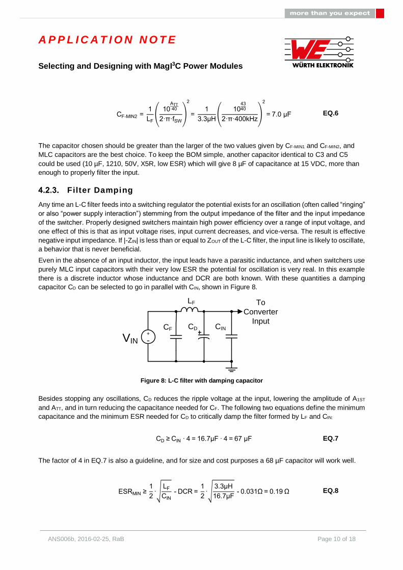
capacitor CD can be selected to go in parallel with CIN, shown in Figure 8.
Figure 8: L-C filter with damping capacitor
Besides stopping any oscillations, CD reduces the ripple voltage at the input, lowering the amplitude of A1ST
and ATT, and in turn reducing the capacitance needed for CF. The following two equations define the minimum
capacitance and the minimum ESR needed for CD to critically damp the filter formed by LF and CIN:
The factor of 4 in EQ.7 is also a guideline, and for size and cost purposes a 68 µF capacitor will work well.
+
-VIN
CD CIN
To
Converter
InputCF
LF
CF-MIN2 = 1
LF
(10
ATT40
2·π·fSW
)
2
= 1
3.3µH(
104340
2·π·400kHz)
2
= 7.0 µF EQ.6
CD ≥ CIN · 4 = 16.7µF · 4 = 67 µF EQ.7
ESRMIN ≥ 1
2·√
LF
CIN
- DCR = 1
2·√
3.3µH
16.7µF - 0.031Ω = 0.19 Ω EQ.8

ANS006b, 2016-02-25, RaB Page 11 of 18
A P P L I C A T I O N N O T E
Selecting and Designing with MagI3C Power Modules
A negative value for the minimum ESR would indicate that the inductor DCR already provides enough
damping resistance. The typical choice for CD is an aluminum electrolytic capacitor. Surface mount aluminum
capacitors rated to 50V with 68 µF are available in several sizes from Würth Elektronik eiSos. What´s more,
for damping the normally “bad” characteristic of high ESR is actually helpful for damping. The Würth Elektronik
WCAP-ASLL Capacitor 865 060 653 009 is a surface mount aluminum electrolytic capacitor rated at 50 V that
provides 68 µF with an impedance of 0.34 Ω in a compact 8 mm radius footprint, with a height of 10.5 mm.
This capacitor will make an excellent damper.
5. PCB Layout _________________________________________________
5.1. Identifying the Critical Current Loops
Power Modules with integrated MOSFETs and power magnetics enjoy a definite advantage over discrete
solutions with regards to EMI because they reduce the area of the loops carrying heavy switched current to
mere square millimeters. Lower loop area means lower inductance, and the noise or EMI induced is:
Therefore reducing loop area/inductance is critical to achieving the best EMC performance. A switching
regulator can be analyzed by drawing the flow of current as loops during the two parts of the switching cycle,
and the buck converter is shown in Figure 9, with the current during the control MOSFET on-time in orange
and during the synchronous MOSFET on-time in blue.
Figure 9: Synchronous buck converter current loops. Control MOSFET in orange, synchronous MOSFET in blue
Once the current loops have been drawn, the technique is to identify the sections with heavy, switched
current. These are:
1. Sections that only have one color, such as the sections through each MOSFET, and also from the
source of the synchronous MOSFET back to the negative connection of the input capacitor.
2. Sections where heavy current flows in one direction during the first part of the switching cycle, and
then changes direction during the second portion of the cycle.
It is often helpful to redraw the circuit again and clearly mark these critical, high di/dt sections:
+
- D
SYNC
FET
CONTROL FET
VEMI = LParasitic·di
dt EQ.9

ANS006b, 2016-02-25, RaB Page 12 of 18
A P P L I C A T I O N N O T E
Selecting and Designing with MagI3C Power Modules
Figure 10: Synchronous buck converter with the critical area drawn in green
The green area in Figure 10 deserves priority when laying out the PCB. Figure 10 also presents a technique
used to make the best use of the input capacitors, which is to route the source of the synchronous MOSFET
directly to the negative connection of the input capacitor before connecting to system ground. In this way the
lowest value input capacitor can filter any high frequency noise generated by the switching of the MOSFETs.
Figure 1 shows that these two layout techniques are already implemented when using a MagI³C Power Module
because a 0.47 µF multi-layer ceramic (MLC) capacitor is included, placed in as tight a loop as possible with
the control MOSFET and synchronous MOSFET. All that remains is to place the external input capacitors as
close as possible to the VIN and PGND pins/exposed pad.
Placing the output capacitors still deserves some attention, and the simple pinout of the MagI³C series makes
it easy to minimize the less critical loop area between the output capacitors and the VOUT and PGND
pins/exposed pad.
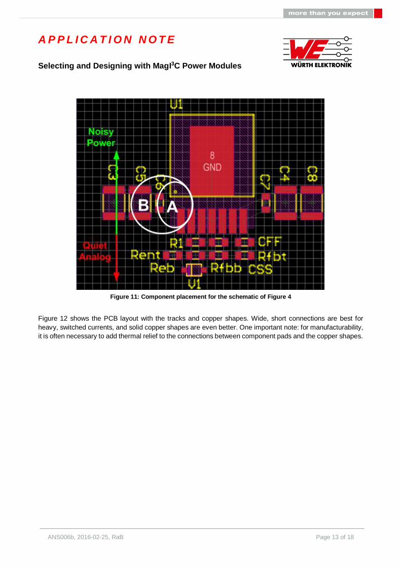
5.2. Placing Components
In standard switching regulators the switching node (where the two power switches and one side of the
inductor/transformer meet) is the most critical portion due to the rapidly switching currents with parasitic
inductance and due to capacitive coupling while switching high voltages. However in a MagI³C Module this
node is internal to the device and the layout of the two power MOSFETs and inductor are completely optimized.
This leaves only the input and output capacitors. In buck regulators the input side has the heavy switched
currents, so the input capacitors should be routed first. The smaller the capacitor and the capacitance value,
the higher the frequency that a capacitor will filter, so the smallest, lowest value capacitors should go in the
tightest loop – the loop with the lowest parasitic inductance – in order to best filter high frequency noise. This
is Loop A as shown in Figure 11, enclosing 1 µF capacitor C6. Larger and higher value capacitors such as C3
and C5 come next, in Loop B. Bulk capacitors such as aluminum can be farther away, since their job is to
dampen oscillations and filter ripple at the switching frequency. An input L-C filter as discussed in Section 4.2
and shown in Figure 6 goes between C3 and the input connectors along the bottom of the MagI³C Power
Module evaluation boards.
Figure 11 includes green and red arrows indicating the general separation of the power side, where switching
currents and fast transients generate lots of EMI, and the control, or analog side, where sensitive, high
impedance nodes such as the FB and EN pins are located. Keep all the power flow on one side, and the
sensitive portions of the circuit on the other side of the PCB whenever possible.
+
- D
ANS006b, 2016-02-25, RaB Page 13 of 18
A P P L I C A T I O N N O T E
Selecting and Designing with MagI3C Power Modules
Figure 11: Component placement for the schematic of Figure 4
Figure 12 shows the PCB layout with the tracks and copper shapes. Wide, short connections are best for
heavy, switched currents, and solid copper shapes are even better. One important note: for manufacturability,
it is often necessary to add thermal relief to the connections between component pads and the copper shapes.

ANS006b, 2016-02-25, RaB Page 14 of 18
A P P L I C A T I O N N O T E
Selecting and Designing with MagI3C Power Modules
Figure 12: Power Planes and Connections
5.3. Maximizing the Beneficial Parasitic Capacitance
The word “parasitic” is associated with negative effects, but PCB layout engineers can take advantage of
beneficial parasitic effects, such as capacitance between the VIN net to GND or the VOUT net to GND by
placing the edges of copper shapes with these nets close to one another on the same layer and by adding
solid planes to the other PCB layers. Figure 12 shows a simple, two layer PCB. Excepting the feedback (FB)
pin trace, the entire bottom layer is dedicated to GND, and the capacitance between this plane and the areas
on the top layer connected to VIN and VOUT adds 100 – 1000 pF of capacitance that is very helpful for filtering
high frequency noise. Flooding the unused areas of the PCB with copper connected to low impedance nets
like VIN, VOUT and GND improves both EMC and thermal performance (see the following section) but does
not increase the cost of the PCB.
DC-DC regulators like the MagI³C Modules normally operate on isolated secondaries and should follow
functional isolation guidelines for minimum spacing of different nets. Functional spacing guidelines in safety
standards like IEC60950 can be difficult to interpret. UL796 provides a more practical approach based upon
the minimum distances to prevent arcing, and this document specifies 1 mm of clearance for every 1600 V
(peak or DC). For the top layer in Figures 10 and 11, the maximum voltage difference is 42 VDC between VIN
and GND, which corresponds to a minimum distance of 0,026 mm.

ANS006b, 2016-02-25, RaB Page 15 of 18
A P P L I C A T I O N N O T E
Selecting and Designing with MagI3C Power Modules
Figure 13: Flooding the bottom layer (in blue) adds helpful parasitic capacitance
from VIN to GND and from VOUT to GND
Designing the PCB for best manufacturability is also important, and although the limits can vary from one PCB
manufacturer to the next, quick-turn PCB makers often supply a clear set of guidelines. The thicker the copper
the greater the spacing needs to be. For example, for 35 µm copper thickness a minimum spacing of 0,175
mm is typical, and for 70 µm copper thickness a typical spacing is 0.25 mm. After taking into account the
electrical spacing requirements and the manufacturing requirements, the PCB in Figures 10 and 11 was
designed with 0.4 mm from VIN to GND and from VOUT to GND. This makes the design electrically safe,
affordable to manufacture and still provides good capacitive coupling between the input and output voltages
and system GND.
6. Thermal Recommendations ____________________________________
The TO263-7EP package (VDRM family) is a high power, surface mount device. In many applications adding
a heatsink is impractical, so the best way to draw heat away from the modules is with the PCB itself. The
thermal resistance from the source of the heat (mainly the power MOSFETs) to the ambient air, ΘJA can be
lowered using the following PCB design techniques:
1. Increasing the thickness of the copper plating
2. Increasing the area of solid copper connected to the thermal tab/pad
3. Adding thermal vias to connect the thermal tab/pad to solid planes of copper on the internal and bottom
layers
4. Increasing the thickness of the thermal via barrel plating. Also filling the vias with solder, or even filling
the vias with copper plugs
5. Increasing the airflow parallel to the copper planes that are connected to the thermal tab/pad

ANS006b, 2016-02-25, RaB Page 16 of 18
A P P L I C A T I O N N O T E
Selecting and Designing with MagI3C Power Modules
The thermal tab of the TO-263 and the exposed pad of the TO-263-7EP package are connected electrically to
PGND, making it easy to connect them to large areas of copper without compromising the electrical or EMC
performance of the modules. Figures 12 and 13 show how the copper area on both the top and bottom layers
has been extended. Figure 14 shows the recommended arrangement of thermal vias to connect the power
tab/pad to the internal layers and the bottom layer: a grid of 36 vias arranged in a 6 x 6 array, with inner
diameters of 0,254 mm and outer diameters of 0,508 mm. The entire area underneath the thermal tab/pad
should be always filled with thermal vias, however further vias outside this area show quickly diminishing
returns.
Figure 14: Recommended size and distribution of thermal vias. TO263-7EP shown
6.1. Manufacturability
When adding these thermal vias it is always worthwhile to consult the PCB manufacturer and confirm the
manufacturability. For example, it may decrease cost significantly to increase the hole size to 0.3 mm, or to
increase the outer diameter slightly to 0.6 mm, and these changes will have little effect on the heat transfer.
Likewise, increasing the thickness of the vias´ copper plating, filling them with solder or with copper plugs can
increase the PCB cost to unreasonable levels. Good quality PCB manufacturers can help recommend the best
compromise of cost to thermal performance.

ANS006b, 2016-02-25, RaB Page 17 of 18
A P P L I C A T I O N N O T E
Selecting and Designing with MagI3C Power Modules
6.2. Thermal Design Example
This example will examine the thermal requirements for the circuit and BOM of Figure 6, under the following
conditions:
VIN = 24 VDC, VOUT = 12 VDC, IOUT-MAX = 3 A, fSW = 400 kHz, TA = 50 ºC
The first step is to determine the total power dissipation, which can be read from the curves in the
WPMDH1302401JT datasheet and is 2.9 W. For this example the maximum permissible junction temperature
(the internal temperature of the module), TJ-MAX will be 100ºC. Then the maximum permissible junction-to-
ambient thermal resistance, ΘJA-MAX can be determined as follows:
The result shows that this will be a challenging thermal design, since the datasheet´s Electrical Characteristics
table lists a ΘJA of 16ºC/W using a four layer PCB with 35 µm copper measuring 76.2 x 76,2 mm. To estimate
the PCB area the junction-to-case thermal resistance, ΘJC, can be read from the datasheet as 1.9 ºC/W. This
low value indicates that the TO263-7EP package was created with high power dissipation in mind. The
minimum PCB area in square centimeters is then:
Note: the factor of 500 represents a simplification and approximation of several, more complex factors
An area of 33 cm2 corresponds to a square PCB measuring 5.7 x 5.7 cm, with four layers of at least 35 µm
copper that uses the thermal via pattern given in Figure 14. The results match the datasheet values for ΘJA,
ΘJC and the PCB area to some extent, but it is clear that thermal calculations are not exact. Once again, the
importance of actual lab testing must be stressed. Also, as detailed at the beginning of this section, increasing
the copper thickness, filling the thermal vias or increasing airflow will all help with the following: allowing a
smaller PCB area while maintaining the same maximum junction temperature, or lowering the maximum
junction temperature while maintaining the same PCB area.
θJA-MAX = TJ-MAX - TA
PD
= 100°C - 50°C
2.9W = 17.2
°C
W EQ.10
APCB-MIN = 500
°C · cm²W
θJA-MAX - θJC
= 500
°C · cm²W
17.2°CW
- 1.9°CW
= 33 cm² EQ.11

ANS006b, 2016-02-25, RaB Page 18 of 18
A P P L I C A T I O N N O T E
Selecting and Designing with MagI3C Power Modules
I M P O R T A N T N O T I C E
The Application Note is based on our knowledge and experience of typical requirements concerning these areas. It serves
as general guidance and should not be construed as a commitment for the suitability for customer applications by Würth
Elektronik eiSos GmbH & Co. KG. The information in the Application Note is subject to change without notice. This
document and parts thereof must not be reproduced or copied without written permission, and contents thereof must not
be imparted to a third party nor be used for any unauthorized purpose.
Würth Elektronik eiSos GmbH & Co. KG and its subsidiaries and affiliates (WE) are not liable for application assistance of
any kind. Customers may use WE’s assistance and product recommendations for their applications and design. The
responsibility for the applicability and use of WE Products in a particular customer design is always solely within the
authority of the customer. Due to this fact it is up to the customer to evaluate and investigate, where appropriate, and
decide whether the device with the specific product characteristics described in the product specification is valid and
suitable for the respective customer application or not.
The technical specifications are stated in the current data sheet of the products. Therefore the customers shall use the
data sheets and are cautioned to verify that data sheets are current. The current data sheets can be downloaded at
www.we-online.com. Customers shall strictly observe any product-specific notes, cautions and warnings. WE reserves the
right to make corrections, modifications, enhancements, improvements, and other changes to its products and services.
WE DOES NOT WARRANT OR REPRESENT THAT ANY LICENSE, EITHER EXPRESS OR IMPLIED, IS GRANTED
UNDER ANY PATENT RIGHT, COPYRIGHT, MASK WORK RIGHT, OR OTHER INTELLECTUAL PROPERTY RIGHT
RELATING TO ANY COMBINATION, MACHINE, OR PROCESS IN WHICH WE PRODUCTS OR SERVICES ARE USED.
INFORMATION PUBLISHED BY WE REGARDING THIRD-PARTY PRODUCTS OR SERVICES DOES NOT
CONSTITUTE A LICENSE FROM WE TO USE SUCH PRODUCTS OR SERVICES OR A WARRANTY OR
ENDORSEMENT THEREOF.
WE products are not authorized for use in safety-critical applications, or where a failure of the product is reasonably
expected to cause severe personal injury or death. Moreover, WE products are neither designed nor intended for use in
areas such as military, aerospace, aviation, nuclear control, submarine, transportation (automotive control, train control,
ship control), transportation signal, disaster prevention, medical, public information network etc. Customers shall inform
WE about the intent of such usage before design-in stage. In certain customer applications requiring a very high level of
safety and in which the malfunction or failure of an electronic component could endanger human life or health, customers
must ensure that they have all necessary expertise in the safety and regulatory ramifications of their applications.
Customers acknowledge and agree that they are solely responsible for all legal, regulatory and safety-related requirements
concerning their products and any use of WE products in such safety-critical applications, notwithstanding any applications-
related information or support that may be provided by WE. CUSTOMERS SHALL INDEMNIFY WE AGAINST ANY
DAMAGES ARISING OUT OF THE USE OF WE PRODUCTS IN SUCH SAFETY-CRITICAL APPLICATIONS.
U S E F U L L I N K S
Application Notes:
http://www.we-online.com/app-notes
REDEXPERT Design Tool:
http://www.we-online.com/redexpert
Toolbox:
http://www.we-online.com/toolbox
Product Catalog:
http://katalog.we-online.de/en/
C O N T A C T I N F O R M A T I O N
Würth Elektronik eiSos GmbH & Co. KG
Max-Eyth-Str. 1, 74638 Waldenburg, Germany
Tel.: +49 (0) 7942 / 945 – 0
Email: [email protected]
Web: http://www.we-online.com