renewable electrochemical fuel production: fundamental principles and materials...
TRANSCRIPT
Renewable electrochemical fuel production: fundamental principles and materials development
By
Joaquin Resasco
A dissertation submitted in partial satisfaction of the
requirements for the degree of
Doctor of Philosophy
in
Chemical Engineering
in the
Graduate Division
of the
University of California, Berkeley
Committee in charge:
Professor Alexis Bell, Chair
Professor Bryan McCloskey
Professor Peidong Yang
Fall 2017

Renewable electrochemical fuel production: Fundamental principles and materials development
© 2017
By
Joaquin Resasco

1
Abstract
Renewable electrochemical fuel production: Fundamental principles and materials development
By
Joaquin Resasco
Doctor of Philosophy in Chemical Engineering
University of California, Berkeley
Professor Alexis Bell, Chair
Direct solar to fuel conversions offer an attractive and sustainable alternative to the use of
fossil fuels an energy source. Electrochemical reactions can produce fuels that act as an energy
storage medium for intermittent solar energy. However, current limitations in both materials
development and fundamental understanding of electrochemical processes has limited the
efficiency of photoelectrochemical systems. In the first portion of this dissertation, we discuss
the simplest electrochemical process for producing a fuel using solar energy: water splitting to
form hydrogen and oxygen. For this reaction, we discuss how materials development strategies
can be developed to maximize the performance of the catalytic and light absorbing components
of a photoelectrode. In particular we explore how one dimensional nanostructures can be utilized
to improve performance for water oxidation. Although these nanostructures have several
beneficial properties, their applicability can be hindered by difficulty in tuning the material
composition without sacrificing morphology and material quality. In the first study, we present a
method for controlling the composition of metal oxide nanowires without changing their
morphology or crystallinity. In particular using this method based on solid state diffusion, and a
novel process for manganese oxide atomic layer deposition, we produced manganese doped
rutile TiO2 nanowires. Using a variety of physical characterization techniques, it was determined
that Mn could be incorporated as a substitutional dopant for Ti in the rutile lattice. We
investigated how this compositional control allows for modification of the optical, electronic,
and electrochemical properties of the semiconductor nanowire. The doping process resulted in an
enhancement in the electrocatalytic activity for water oxidation, consistent with theoretical
predictions. This demonstrated that this simple and general method could be used to control the
properties of one-dimensional nanostructures.
2
We then utilized this technique to improve upon the efficiency of light absorbing
photoandoes for water oxidation. Metal oxides that absorb visible light such as monoclinic
BiVO4 are attractive for use in this application. However, their performance is often limited by
poor charge carrier transport. We investigated the possibility of addressing this issue by using
separate materials for light absorption and carrier transport. As a carrier transport material, we
used TiO2 nanowires, modified with a Ta dopant to improve the conductivity. The doping
process was accomplished using the previously mentioned solid state diffusion technique. BiVO4
was added to these conductive nanowire arrays as a visible light sensitizer. Electrochemical and
spectroscopic measurements were used to provide experimental evidence for the correct band
alignment needed for favorable electron transfer from BiVO4 to TiO2. This host−guest nanowire
architecture allows for the benefits of both materials to be taken advantage of, resulting in both
high light absorption and carrier collection efficiency. This system resulted in an onset of anodic
photocurrent near 0.2 V vs RHE, and a photocurrent density of 2.1 mA/cm2 at 1.23 V vs RHE.
In the second portion of this work, we discuss the more complex reaction of carbon
dioxide reduction. This reaction is appealing because it can produce more energy dense
carbonaceous fuels, rather than hydrogen. While this is an appealing prospect, the efficiency of
CO2 reduction systems is currently lower than those for water splitting. One reason for this is that
the fundamental understanding of electrochemical processes for this reaction are still lacking,
particularly in how the conditions used for testing catalysts for this reaction can significantly
impact the measured performance. In particular, it has been shown that the choice of both
electrolyte cation and anion has an impact on the measured electrocatalyst performance. In the
final works we seek to develop a deeper understanding of these effects using a combination of
experimental and theoretical methods.
The first study focuses on the effect of alkali metal cations on the on the intrinsic activity
and selectivity of metal catalysts for the reduction of CO2. Experiments were conducted under
conditions where mass transport limitations were minimal to show that cation size affects the
intrinsic rates of formation of certain reaction products. Over Cu oriented thin films, increasing
cation size increased rates of production of HCOO-, C2H4, and C2H5OH, while CO and HCOO-
rates increased over polycrystalline Ag and Sn. Reduction of key reaction intermediates
identified the elementary reaction steps affected by cation size, namely the activation of CO2 and
the formation of carbon carbon bonds. Density functional theory calculations demonstrated that
the alkali metal cations influence the CO2 reduction reaction due to electrostatic interactions
between solvated cations present at the outer Helmholtz plane and polarizable adsorbed species.
The observed trends in activity with cation size are attributed to an increase in the concentration
of cations at the outer Helmholtz plane with increasing cation size.
The next study presents a combination of experimental and computational studies aimed
at understanding the role of electrolyte anions on the reduction of CO2 over Cu surfaces. The
effects of bicarbonate buffer concentration and identity on the rates of formation of the major
products formed by reduction of CO2 over Cu was investigated experimentally. It was
demonstrated that the composition and concentration of electrolyte anions has relatively little
effect on the formation of CO, HCOO-, C2H4, and CH3CH2OH, but significantly affects the
formation of H2 and CH4. Numerical simulations were used to assess the magnitude of changes
in pH at the electrode surface for different electrolytes. The influence of pH on the activity of Cu
for producing H2 and CH4 was also considered. It was determined that these differences in pH at

3
electrode surface were insufficient to explain the trends in activity and selectivity observed with
changes in anion buffering capacity observed for the formation of H2 and CH4. We therefore
proposed that these differences are the result of the ability of buffering anions to donate
hydrogen directly to the electrode surface and in competition with water. The effectiveness of
buffering anions to serve as hydrogen donors is found to increase with decreasing pKa of the
buffering anion. This understanding of how electrochemical conditions affect measured activity
can lead to insights into how to maximize efficiency of CO2 reduction systems.

i
To my parents, Daniel and Teresita.

ii
Table of contents
Acknowledgements
Chapter 1: Introduction
1.1 Abstract
1.2 Introduction to water splitting
1.3 Development of nanostructured materials for water splitting
1.3.1 Current limitations for solar water splitting devices
1.3.2 Semiconductor Nanowires for Solar Fuel Generation: Advantages and Challenges
1.4 Fundamental principles of carbon dioxide reduction
1.5 Outline
1.6 References
Chapter 2: Uniform doping of metal oxide nanowires using solid state diffusion.
2.1 Abstract
2.2 Introduction
2.3 Experimental methods
2.3.1 Synthesis of titanium dioxide nanowire arrays
2.3.2 Atomic layer deposition of manganese oxide
2.3.3 Conversion process
2.3.4 Physical and chemical characterization
2.3.5 Electrochemical characterization
2.4 Results and discussion
2.5 Conclusions
2.6 References

iii
Chapter 3: Nanowire Heterostructure Photoanodes based on Type II Band Alignment.
3.1 Abstract
3.2 Introduction
3.3 Experimental methods
3.3.1 Synthesis of titanium dioxide nanowire arrays
3.3.2 Atomic layer deposition
3.3.3 Conversion process
3.3.4 Synthesis of bismuth vanadate
3.3.5 Physical and chemical characterization
3.3.6 Electrochemical characterization
3.4 Results and discussion
3.4.1 Development of a nanowire heterostructured photoanode
3.4.2 Synthesis of Ta:TiO2 conductive nanowire scaffolds
3.4.3 Coating TiO2 nanowires with visible light absorber BiVO4
3.4.4 Photoelectrochemistry of nanowire heterostructures
3.4.5 Band alignment of TiO2 and BiVO4
3.4.6 Electron transfer between TiO2 and BiVO4
3.5 Conclusions
3.6 References
Chapter 4: Standard methods for measuring and reporting catalytic data for
electrochemical CO2 reduction
4.1 Introduction
4.2 Considerations when measuring electrocatalytic activity
4.2.1 Impact of impurities on electrocatalytic activity
4.2.2 Impact of mass transport limitations on electrocatalytic activity
4.2.3 Reporting electrocatalytic activity
4.2.4 Summary of experimental methods for measuring electrocatalytic activity
4.2.5 Reproducibility in electrocatalytic activity measurements
4.3 References
iv
Chapter 5: Promoter effects of alkali metal cations on the electrochemical reduction of
carbon dioxide
5.1 Abstract
5.2 Introduction
5.3 Experimental and computational methods
5.3.1 Electrode preparation
5.3.2 Electrode characterization
5.3.3 Electrochemical measurements
5.3.4 Product analysis
5.3.5 Theoretical calculations
5.4 Results
5.4.1 Cation effects on Cu(100) and Cu(111) oriented films
5.4.2 Relative effects of alkali metal cations
5.4.3 Cation effect on polycrystalline Ag and Sn
5.4.4 Cation effects on elementary reaction steps: reduction of intermediates
5.5 Discussion
5.5.1 Cation promoter effects
5.6 Conclusions
5.7 References
Chapter 6: Effects of anion identity and concentration on electrochemical reduction of CO2
6.1 Abstract
6.2 Introduction
6.3 Experimental and computational methods
6.3.1 Electrode preparation
6.3.2 Electrode characterization
6.3.3 Electrolyte preparation
6.3.3 Electrochemical measurements
6.3.4 Product analysis
6.3.5 Numerical simulations

v
6.4 Results and discussion
6.4.1 Buffer concentration effects on the activity of Cu(100) oriented films
6.4.2 Surface pH effects for bicarbonate buffer electrolytes
6.4.3 Buffering anions as a hydrogen source
6.4.4 Buffer identity effects on the activity of Cu(100) oriented films
6.4.5 Surface pH effects for different buffer electrolytes
6.5 Conclusions
6.6 References

vi
Acknowledgements
I would first like to thank Professor Alex Bell for the opportunity to work with him over
the last few years. Your guidance and mentorship has made me a better and more thoughtful
scientist. Your dedication and enthusiasm for science over your extensive career will be a
constant source of inspiration for me going forward. I have greatly enjoyed my time working
with you. I would also like to thank Professor Peidong Yang for also allowing me to work in
such an exciting research environment. Your commitment to research has motivated me to
always strive further in approaching scientific problems.
I would also like to thank other faculty members who have been very supportive of me
throughout my time in Berkeley. To Professor Enrique Iglesia, I am very grateful for your advice
and support, and for being a role model to me in both teaching and research. I would also like to
thank Professor Tom Jaramillo at Stanford University, for his positivity and mentorship
throughout my graduate experience.
I have had the privilege of working with many incredibly talented and friendly
researchers at Berkeley. The time I spent working with you has made my graduate research both
educational and enjoyable, and I wish you all the best of luck in your future. In particular I must
thank Nick Kornienko, Nigel Becknell, and Anthony Fu, who managed to make late nights at the
synchrotron fun. Thanks also to Sean Andrews, for keeping humor alive in the lab. Chong Liu
and Neil Dasgupta, thank you for being great teachers when I was getting started in research. To
Hao Zhang, Yude Su, and Yanwei Lum, thank you for being great labmates. I must also give a
special thanks to Ezra Clark, who has been both a great friend and research teammate. I must
also thank the great coworkers and collaborators I have had from outside Berkeley, in particular
Professor Alex Briseno, Karen Chan, Leanne Chen, and Charlie Tsai.
To all of my friends, both the ones I made in Berkeley, and my friends from home, thank
you for being there. To my dearest friend, Stella, thank you for putting a smile on my face every
day.
I would not be here were it not for my wonderful family. To my mother, Teresita, thank
you for your selfless love and support. To my father, Daniel, you are my greatest teacher and role
model. Thank you both for everything that you have done for me. To my brothers and sisters,
thank you for all that you do.
And finally to Ieva, thank you for being my companion through graduate school and
making the last five years so enjoyable. I look forward to a life of adventures with you.
1
Chapter 1
Introduction to electrochemical energy
conversion reactions
1.1 Abstract
Direct solar to fuel conversions offer an attractive solution to the replacement of fossil
fuels with a sustainable energy source. However, designing efficient, stable, and cost effective
photoelectrochemical systems is hindered by both fundamental understanding of electrochemical
processes, and materials development. We first discuss the simplest electrochemical process for
producing a fuel from sunlight: water splitting to form hydrogen and oxygen. For this more
simple process, we discuss how materials development strategies can be developed to maximize
the performance of the catalytic and light absorbing components of a photoelectrode. We then
discuss the more complex reaction of carbon dioxide reduction, which is appealing due to its
ability to produce more energy dense carbonaceous fuels. We demonstrate that fundamental
understanding of electrochemical processes for this reaction are still lacking, particularly in how
the conditions used for testing catalysts for this reaction can significantly impact the measured
performance. We close with an outlook for future research directions for electrochemical
production of fuels.
1.2 Introduction to water splitting
Finding a carbon neutral source of energy which can replace fossil fuels in a scalable and
cost effective way is one of the most important issues facing modern society.1, 2 Burning fossil
fuels as a source of energy leads to an increased concentration of atmospheric CO2 with an
associated rise in global temperatures, a change with significant environmental consequences.
Collecting energy from sunlight offers a potential solution to this problem. The solar resource is
nearly inexhaustible, as the solar energy striking the earth’s surface exceeds the global energy
demand by over four orders of magnitude.3, 4 However, the intermittent nature of photovoltaic
energy production means that large scale implementation of this technology must be
2
accompanied by an energy storage system.5 Energy storage at the TW scale remains a
challenging problem using existing technologies such as batteries. Therefore, the use of solar
energy to drive chemical reactions to produce chemical fuels such as hydrogen or hydrocarbons
provides an attractive solution that could also fit well into the current energy infrastructure.
The concept of using sunlight to store energy in the form of chemical bonds was first
demonstrated by Fujishima and Honda in 1972.6 In this seminal study anatase TiO2 was used as a
photocatalyst to split water into molecular H2 and O2 without external bias. This
photoelectrochemical (PEC) process contains two distinct processes, the absorption of light
resulting in the generation of excited charge carriers, and the utilization of these carriers to drive
chemical transformations.7 Under illumination, the semiconductor produces excited carriers
which are separated by the built-in electric field resulting from the semiconductor-liquid
junction. The charge carriers are then transported to surface catalytic sites to carry out
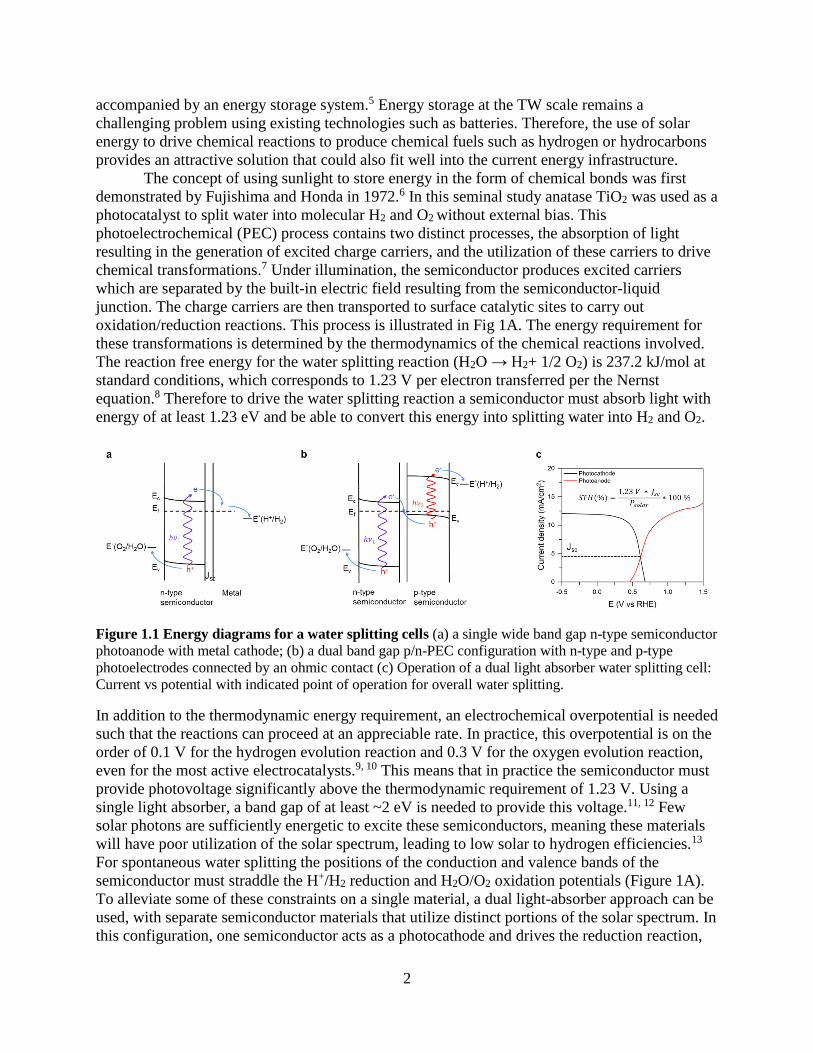
oxidation/reduction reactions. This process is illustrated in Fig 1A. The energy requirement for
these transformations is determined by the thermodynamics of the chemical reactions involved.
The reaction free energy for the water splitting reaction (H2O → H2+ 1/2 O2) is 237.2 kJ/mol at
standard conditions, which corresponds to 1.23 V per electron transferred per the Nernst
equation.8 Therefore to drive the water splitting reaction a semiconductor must absorb light with
energy of at least 1.23 eV and be able to convert this energy into splitting water into H2 and O2.
Figure 1.1 Energy diagrams for a water splitting cells (a) a single wide band gap n-type semiconductor
photoanode with metal cathode; (b) a dual band gap p/n-PEC configuration with n-type and p-type
photoelectrodes connected by an ohmic contact (c) Operation of a dual light absorber water splitting cell:
Current vs potential with indicated point of operation for overall water splitting.
In addition to the thermodynamic energy requirement, an electrochemical overpotential is needed
such that the reactions can proceed at an appreciable rate. In practice, this overpotential is on the
order of 0.1 V for the hydrogen evolution reaction and 0.3 V for the oxygen evolution reaction,
even for the most active electrocatalysts.9, 10 This means that in practice the semiconductor must
provide photovoltage significantly above the thermodynamic requirement of 1.23 V. Using a
single light absorber, a band gap of at least ~2 eV is needed to provide this voltage.11, 12 Few
solar photons are sufficiently energetic to excite these semiconductors, meaning these materials
will have poor utilization of the solar spectrum, leading to low solar to hydrogen efficiencies.13
For spontaneous water splitting the positions of the conduction and valence bands of the
semiconductor must straddle the H+/H2 reduction and H2O/O2 oxidation potentials (Figure 1A).
To alleviate some of these constraints on a single material, a dual light-absorber approach can be
used, with separate semiconductor materials that utilize distinct portions of the solar spectrum. In
this configuration, one semiconductor acts as a photocathode and drives the reduction reaction,
3
while the other acts as a photoanode and drives the oxidation reaction.7 In the two
semiconductors, photogenerated minority carriers will move to the semiconductor liquid junction
where they carry out their respective redox reactions, while majority carriers recombine at the
semiconductor-semiconductor interface. This process is illustrated in Fig 1B. This scheme
greatly relaxes the requirements on the semiconductor materials and allows for significantly
higher theoretical solar to hydrogen efficiencies.11, 12 As the components of a water splitting cell
are electrically connected, the current is matched throughout the device. This means the
efficiency of the device is limited by the performance of the weakest light absorber or surface
cocatalyst.14 Therefore, to achieve high efficiencies, both light absorbers and cocatalysts must be
considered, such that the turnover frequency of the electrocatalyst is sufficient to handle the flux
of photogenerated carriers reaching the surface. Additionally, there must be flux matching
between the two semiconductor photoelectrodes, such that both the photoanode and
photocathode provide the necessary voltage such that the operating point is near the maximum
power point of the two separate light absorbers. This point is illustrated in Fig 1C. To date,
effective matching between all components of the system has not been realized, due primarily to
insufficient catalyst and semiconductor materials development.15
1.3 Development of nanostructured materials for water
splitting
1.3.1 Current limitations for solar water splitting devices
In current water splitting cells, significantly more efficiency limitations are associated
with the oxidation reaction than with the reduction reaction.15 This is true both of the
semiconducting light absorber and of the electrocatalyst.9, 10 For the light absorbing material, this
is due to the problems associated with achieving both high efficiency and operational stability.
Conventional light absorber materials for photovoltaic applications such as Si, and the III-V and
II-VI compounds have been largely unsuccessful because of their poor stability in solution.
Recently, promising work has been done on stabilizing conventional light absorbers such as Si,16
GaAs,17 and InP.18 However, the photovoltage obtained by these materials thus far has been
insufficient to match with smaller band gap photocathode materials such as Si and InP in a dual
absorber photoelectro-synthetic cell.19, 20 Additionally, these materials have high production and
processing costs.
In constrast, many binary oxide materials provide good stability under the highly
oxidizing conditions of water oxidation.21 However, the most commonly studied binary oxide,
TiO2, has a band-gap that is too large to absorb sunlight efficiently (∼3.0 eV), consequently
limiting its achievable photocurrent.22 Small band gap metal oxides that absorb visible light and
can be inexpensively synthesized, such as WO3, Fe2O3, and BiVO4, are alternative materials that
hold promise to overcome these limitations.23-25 Hematite (Fe2O3), has a desirable band gap of
∼2.2 eV, making it a visible light absorber. However, hematite has a conduction band edge at
0.55 V versus the reversible hydrogen electrode (RHE), limiting its theoretical maximum
photovoltage, and extremely poor charge transport properties that have prevented efficient
charge separation. Thus reported efficiencies from hematite lag significantly below theoretical
maximum values. BiVO4 is another promising material due to its relatively small optical band

4
gap of ~2.5 eV and its negative conduction band edge (∼0 V versus RHE).26, 27 Under Air-Mass
1.5 Global (AM1.5G) solar illumination, the maximum achievable photocurrent for water
oxidation using BiVO4 is ~7 mA/cm2.25 However, the water oxidation photocurrent obtained in
practice for BiVO4 again is substantially lower than this value, mainly due to poor carrier
transport properties, with electron diffusion lengths shorter than the film thickness necessary to
absorb a substantial fraction of light.26 The use of nanostructured materials could be particularly
beneficial for these materials with poor carrier transport. In the following section, we describe
how the use of one dimensional nanostructures for this application, and how their material
composition can be controlled to give desired properties.
1.3.2 Semiconductor Nanowires for Solar Fuel Generation: Advantages and
Challenges
One dimensional nanostructured materials, such as nanorods or nanowires, have unique
properties that offer opportunities in a range of applications including solar and thermoelectric
energy conversion, energy storage, and photonics.28 Of particular interest here are their benefits
for solar to fuel conversion. These benefits include enhanced light absorption, charge separation,
and increased surface area for driving redox reactions.14 The one dimensional morphology of the
nanowire decouples the path lengths for light absorption and carrier collection, as they can provide
a long optical path length for light absorption along the length of the nanowires, while minority
carrier collection occurs over the short radial direction of the nanowire.29, 30 This advantage is
particularly important for indirect semiconductors and semiconductors with poor internal quantum
efficiencies.31 The large surface area afforded by the nanowire morphology decreases the
requirements needed for electrocatalysts by diluting the number of charge carriers over a larger
surface area. This means that the activity of each catalytic center, or turnover frequency, can be
lower relative to the case of a planar electrode.
A large number of methods have been developed for synthesizing one dimensional
nanostructures. However, synthesizing multinary one dimensional nanostructures with
compositional tunability, while maintaining control over the morphology and material quality
remains challenging using these traditional synthetic approaches. In chapter 2, we will demonstrate
a new approach for producing multimetallic oxide nanowires with controllable composition. This
composition control is provided by a simple solid state diffusion process that allows the structure
and crystallinity of the desired nanostructure to be preserved. In chapter 3, we will demonstrate
how we can use this method to improve the efficiency of photoanode materials for solar water
splitting. This improvement is based on a host-guest structure, where conductive nanowires are
used a scaffold for visible light absorbing sensitizers, thus allowing simultaneously high light
absorption and carrier collection efficiency.
1.4 Fundamental principles of carbon dioxide reduction
Although water splitting can produce hydrogen, which has some appeal for its high
specific energy (140 kJ/gram), the volumetric energy density of hydrogen is quite low, and
storage and transportation of compressed hydrogen is problematic.32 While renewable hydrogen
is still very useful for a variety of applications, it would be appealing to use a similar solar driven
electrochemical process to produce higher energy density carbon based fuels. The

5
electrochemical reduction of carbon dioxide (CO2) offers an attractive option for doing this,
utilizing CO2 as a source of carbon for the production of transportation fuels and commodity
chemicals using intermittent renewable electricity, such as that produced by wind or solar
energy.
Extensive work has been done on identifying catalysts and understanding the reaction
mechanism for CO2 reduction.33, 34 CO2 can adsorb and be reduced to the two electron reduction
products, carbon monoxide (CO) and formate (HCOO-).35 Carbon monoxide can be reduced
further to produce hydrocarbons and oxygenates.36 Alternatively, as the reduction potentials to
produce these products are close to 0 V vs RHE, water can be reduced to form the undesired side
product H2.37 Hydrocarbons and alcohols, rather than carbon monoxide and formic acid, are the
preferred products of CO2 reduction because of their high energy density. Despite extensive
efforts aimed at identifying electrocatalysts that can produce these products, copper (Cu) remains
the only material capable of doing so with significant yields.33, 36, 38 Nevertheless, Cu requires a
high overpotential (~−1 V versus RHE) and produces a broad spectrum of products.39,37 Clearly,
the discovery of novel means for reducing CO2 to desirable products with higher efficiency and
selectivity is needed. However, objective evaluation of the activity and selectivity of both
standard and novel electrocatalysts is currently hindered by the lack of standardized methods for
measuring and reporting electrocatalytic activity. These issues are significant because the
performance of electrocatalyts is influenced not only by the composition and morphology of the
electrocatalyst itself, but also by the conditions in which the electrocatalyst is tested, and by the
purity of the electrocatalyst and electrolyte. For example, several studies have shown that the
identity of both the cations and anions in the electrolyte can affect the activity of a catalyst and
its selectivity to different products.39, 40 However, understanding of the physical processes by
which these species affect catalytic activity is still lacking. Developing this understanding of the
fundamental processes occurring at the electrode surface, including both metal-adsorbate
interactions, as well as the effects of solvation and interfacial electric fields is a first step in the
direction of developing more efficient systems for reducing CO2 to useful products.
1.5 Outline
Motivated by the above discussions, this thesis will begin by summarizing the results of
materials development for photoelectrode systems for water oxidation. In chapter 2, we will
demonstrate a new approach for producing multimetallic oxide nanowires with controllable
composition. This composition control is provided by a simple solid state diffusion process that
allows the structure and crystallinity of the desired nanostructure to be preserved. In chapter 3, we
will demonstrate how we can use this method to improve the efficiency of photoanode materials
for solar water splitting. This improvement is based on a host-guest structure, where conductive
nanowires are used a scaffold for visible light absorbing sensitizers, thus allowing simultaneously
high light absorption and carrier collection efficiency.
Following this, we will summarize work done based on developing an understanding of
the fundamental principles involved in electrochemical reduction of CO2. Electrochemical CO2
reduction provides a potentially more interesting, but less well understood solar to fuel process
relative to water splitting. We will begin in chapter 4 by developing a methodology for accurately
measuring and reporting electrocatalyst performance for CO2 reduction. Then, using this

6
methodology we will discuss how the electrochemical environment affects the catalytic
performance measured. In chapter 5 we will discuss the effect of electrolyte cations on CO2
reduction, and in chapter 6 we will discuss the effect of anions on CO2 reduction. We will close
with an outlook on how this information can be used in practical systems for CO2 reduction.
1.6 References
1. Lewis, N. S.; Nocera, D. G. Proc. Natl. Acad. Sci. 2006, 103, (43), 15729-15735.
2. Chu, S.; Majumdar, A. Nature 2012, 488, (7411), 294-303.
3. Barber, J. Chem. Soc. Rev. 2009, 38, (1), 185-196.
4. Blankenship, R. E.; Tiede, D. M.; Barber, J.; Brudvig, G. W.; Fleming, G.; Ghirardi, M.;
Gunner, M. R.; Junge, W.; Kramer, D. M.; Melis, A.; Moore, T. A.; Moser, C. C.; Nocera, D. G.;
Nozik, A. J.; Ort, D. R.; Parson, W. W.; Prince, R. C.; Sayre, R. T. Science 2011, 332, (6031),
805-809.
5. Gray, H. B. Nat. Chem. 2009, 1, 7.
6. Fujishima, A.; Honda, K. Nature 1972, 238, 37.
7. Walter, M. G.; Warren, E. L.; McKone, J. R.; Boettcher, S. W.; Mi, Q.; Santori, E. A.;
Lewis, N. S. Chem. Rev. 2010, 110, (11), 6446-6473.
8. Tachibana, Y.; Vayssieres, L.; Durrant, J. R. Nat. Photonics 2012, 6, 511.
9. McCrory, C. C. L.; Jung, S.; Peters, J. C.; Jaramillo, T. F. J. Am. Chem. Soc. 2013, 135,
(45), 16977-16987.
10. McCrory, C. C. L.; Jung, S.; Ferrer, I. M.; Chatman, S. M.; Peters, J. C.; Jaramillo, T. F.
J. Am. Chem. Soc. 2015, 137, (13), 4347-4357.
11. Seitz, L. C.; Chen, Z.; Forman, A. J.; Pinaud, B. A.; Benck, J. D.; Jaramillo, T. F.
ChemSusChem 2014, 7, (5), 1372-85.
12. Hu, S.; Xiang, C.; Haussener, S.; Berger, A. D.; Lewis, N. S. Energy Environ. Sci. 2013,
6, (10), 2984.
13. Shockley, W.; Queisser, H. J. J. Appl. Phys. 1961, 32, (3), 510-519.
14. Liu, C.; Dasgupta, N. P.; Yang, P. Chem. Mater. 2014, 26, (1), 415-422.
15. McKone, J. R.; Lewis, N. S.; Gray, H. B. Chem. Mater. 2014, 26, (1), 407-414.
16. Chen, Y. W.; Prange, J. D.; Duhnen, S.; Park, Y.; Gunji, M.; Chidsey, C. E.; McIntyre, P.
C. Nat. Mater. 2011, 10, (7), 539-44.
17. Hu, S.; Shaner, M. R.; Beardslee, J. A.; Lichterman, M.; Brunschwig, B. S.; Lewis, N. S.
Science 2014, 344, (6187), 1005-1009.
18. Sun, K.; Kuang, Y.; Verlage, E.; Brunschwig, B. S.; Tu, C. W.; Lewis, N. S. Adv. Energy
Mater. 2015, 5, 1402276.
19. Boettcher, S. W.; Warren, E. L.; Putnam, M. C.; Santori, E. A.; Turner-Evans, D.;
Kelzenberg, M. D.; Walter, M. G.; McKone, J. R.; Brunschwig, B. S.; Atwater, H. A.; Lewis, N.
S. J. Am. Chem. Soc. 2011, 133, (5), 1216-9.
20. Lee, M. H.; Takei, K.; Zhang, J.; Kapadia, R.; Zheng, M.; Chen, Y. Z.; Nah, J.;
Matthews, T. S.; Chueh, Y. L.; Ager, J. W.; Javey, A. Angew. Chem. Int. Ed. 2012, 51, (43),
10760-4.
21. Ni, M.; Leung, M. K. H.; Leung, D. Y. C.; Sumathy, K. Renew. Sust. Energy Rev. 2007,
11, (3), 401-425.
7
22. Chen, Z.; Jaramillo, T. F.; Deutsch, T. G.; Kleiman-Shwarsctein, A.; Forman, A. J.;
Gaillard, N.; Garland, R.; Takanabe, K.; Heske, C.; Sunkara, M.; McFarland, E. W.; Domen, K.;
Miller, E. L.; Turner, J. A.; Dinh, H. N. J. Mater. Res. 2011, 25, (01), 3-16.
23. Liu, X.; Wang, F.; Wang, Q. Phys. Chem. Chem. Phys. 2012, 14, (22), 7894-911.
24. Sivula, K.; Le Formal, F.; Gratzel, M. ChemSusChem 2011, 4, (4), 432-49.
25. Park, Y.; McDonald, K. J.; Choi, K. S. Chem. Soc. Rev. 2013, 42, (6), 2321-37.
26. Rettie, A. J. E.; Lee, H. C.; Marshall, L. G.; Lin, J.-F.; Capan, C.; Lindemuth, J.; McCloy,
J. S.; Zhou, J.; Bard, A. J.; Mullins, C. B. J. Am. Chem. Soc. 2013, 135, (30), 11389-11396.
27. Kim, T. W.; Choi, K.-S. Science 2014, 343, (6174), 990-994.
28. Dasgupta, N. P.; Sun, J.; Liu, C.; Brittman, S.; Andrews, S. C.; Lim, J.; Gao, H.; Yan, R.;
Yang, P. Adv. Mater. 2014, 26, (14), 2137-2184.
29. Su, Y.; Liu, C.; Brittman, S.; Tang, J.; Fu, A.; Kornienko, N.; Kong, Q.; Yang, P. Nat.
Nanotechnol. 2016, 11, 609.
30. Kelzenberg, M. D.; Boettcher, S. W.; Petykiewicz, J. A.; Turner-Evans, D. B.; Putnam,
M. C.; Warren, E. L.; Spurgeon, J. M.; Briggs, R. M.; Lewis, N. S.; Atwater, H. A. Nat. Mater.
2010, 9, 239.
31. Kayes, B. M.; Atwater, H. A.; Lewis, N. S. J. Appl. Phys. 2005, 97, (11), 114302.
32. Züttel, A. Mater. Today 2003, 6, (9), 24-33.
33. Hori, Y., Electrochemical CO2 Reduction on Metal Electrodes. In Modern Aspects of
Electrochemistry, Vayenas, C. G.; White, R. E.; Gamboa-Aldeco, M. E., Eds. Springer New
York: New York, NY, 2008; pp 89-189.
34. Peterson, A. A.; Abild-Pedersen, F.; Studt, F.; Rossmeisl, J.; Norskov, J. K. Energy
Environ. Sci. 2010, 3, (9), 1311-1315.
35. Hansen, H. A.; Varley, J. B.; Peterson, A. A.; Nørskov, J. K. J. Phys. Chem. Lett. 2013,
4, (3), 388-392.
36. Hori, Y.; Wakebe, H.; Tsukamoto, T.; Koga, O. Electrochim. Acta 1994, 39, (11), 1833-
1839.
37. Kuhl, K. P.; Cave, E. R.; Abram, D. N.; Jaramillo, T. F. Energy Environ. Sci. 2012, 5,
(5), 7050-7059.
38. Kuhl, K. P.; Hatsukade, T.; Cave, E. R.; Abram, D. N.; Kibsgaard, J.; Jaramillo, T. F. J.
Am. Chem. Soc. 2014, 136, (40), 14107-14113.
39. Hori, Y.; Murata, A.; Takahashi, R. J. Chem. Soc. Faraday Trans. 1 1989, 85, (8), 2309-
2326.
40. Akira, M.; Yoshio, H. Bull. Chem. Soc. Jpn. 1991, 64, (1), 123-127.
8
Chapter 2
Uniform Doping in Metal Oxide Nanowires
by Solid State Diffusion This chapter contains material from the following publication:
Resasco, J.; Dasgupta, N.P.; Roque-Rosell, J.; Guo, J.; Yang, P. J. Am. Chem. Soc. 2014, 39,
10521.
2.1 Abstract
The synthesis of one-dimensional nanostructures with specific properties is often
hindered by difficulty in tuning the material composition without sacrificing morphology and
material quality. Here, we present a simple solid state diffusion method utilizing atomic layer
deposition to controllably alter the composition of metal oxide nanowires. This compositional
control allows for modification of the optical, electronic, and electrochemical properties of the
semiconductor nanowires. Using this method and a novel process for manganese oxide atomic
layer deposition, we produced manganese doped rutile TiO2 nanowires and investigated their
structural and photoelectrochemical properties. A homogeneous incorporation of the Mn dopant
into the rutile lattice was observed, and the local chemical environment of the Mn was
determined using X-ray absorption spectroscopy. The doping process resulted in a tunable
enhancement in the electrocatalytic activity for water oxidation, demonstrating that this simple
and general method can be used to control the properties of one-dimensional nanostructures for
use in a variety of applications including solar-to-fuel generation.
2.2 Introduction
As discussed in the previous chapter, one dimensional nanostructured materials, such as
nanorods or nanowires, exhibit unique properties that can be exploited in a diverse range of fields
including photoelectrochemistry.1 One dimensional semiconductor nanostructures are beneficial
for use in photoelectrochemistry applications due to the large electrochemically available surface
area afforded by their morphology, the decoupling of light absorption and minority carrier
9
diffusion lengths for efficient charge collection and separation, and enhanced light scattering and
trapping in vertical arrays.2-5
A variety of methods have been developed for synthesizing one dimensional nanostructures
including the vapor-liquid-solid,6, 7 vapor-solid,8 solution-liquid-solid,9 and hydrothermal
methods.10 However, synthesizing ternary or other complex one dimensional nanostructures with
compositional tunability, while maintaining control over the material quality and morphology
remains challenging using traditional synthesis approaches. The simplest method for synthesizing
bulk multinary compound solids is the solid state diffusion method, where reactants are mixed and
heated to allow a diffusive transformation to the thermodynamically favored state. However,
adapting this technique to one dimensional nanostructures requires a technique to uniformly coat
their surfaces with precise control of material loading. One technique that meets this requirement
is atomic layer deposition (ALD).11 ALD is a modified form of chemical vapor deposition (CVD)
based on sequential, self-limiting surface reactions. Due to the saturation of the substrate surface
with the reactant species after each half-cycle, highly conformal films can be deposited on high
aspect ratio structures with sub-nanometer control of film thickness. This technique has been
previously demonstrated to precisely tune the optical and electrochemical properties of nanowires
by fabrication of uniform core-shell structures.12, 13 Here we demonstrate that a solid state diffusion
process for one dimensional nanostructures can be achieved using ALD to precisely control the
surface coating thickness, which is followed by a post annealing step. This approach provides a
general method for producing doped or ternary metal oxide nanostructures with compositional
control while maintaining the desired morphology.
In this chapter, we demonstrate the compositional control afforded by this method and
show its utility for photoelectrochemical water splitting. TiO2 has been the most widely studied
material in this field since Fujishima and Honda’s first demonstration of unassisted solar water
splitting.14 Although the wide band gap of TiO2 limits the achievable photocurrent due to the
limited number of solar photons in the ultraviolet range, transition metal doping of TiO2 can lead
to visible light absorption, potentially increasing the maximum achievable efficiency.15-17
Additionally, theoretical and experimental investigations have shown that transition metal doping
of TiO2, particularly with Mn and Cr, increases the catalytic activity for the oxygen evolution
reaction (OER).18-20 Changing the catalytic activity in this way relies on the ability to introduce
the dopants without modifying the original crystal structure, such that the binding strength of the
surface to the reaction intermediates can be precisely altered.
This conversion chemistry approach provides a high degree of synthetic control, allowing
for the study of the effect of changes in composition on the catalytic activity. We utilize this method
to produce Mn doped TiO2 nanowire arrays and study their photoelectrochemical properties. In
subsequent chapters, we will further demonstrate the generality of this method using other
compositions and its applicability to modify other material properties of interest in
photoelectrochemistry.

10
2.3 Experimental methods
2.3.1 Synthesis of titanium dioxide nanowire arrays
Titanium dioxide (TiO2) nanowires were synthesized by a hydrothermal method.10 In a
typical synthesis, 83 μL of titanium isopropoxide (Sigma-Aldrich) was mixed with 5 mL of 6M
hydrochloric acid (Sigma-Aldrich) in a 40 mL telfon vessel. A fluorine-doped tin oxide (FTO)
coated quartz substrate was angled against the wall of the Teflon vessel such that the FTO
surface was facing down. The Teflon vessel was loaded in a stainless steel autoclave and heated
to 210°C for 150 min. After cooling, the substrates were thoroughly rinsed in deionized water,
yielding single crystalline rutile-TiO2 nanowire arrays. For higher temperature annealing, a TiO2
thin film (~30 nm) was deposited on a quartz substrate as a seeding layer for nanowire growth.
2.3.2 Atomic layer deposition of manganese oxide
Deposition of MnOx thin films was performed in a customized thermal ALD reactor. The
precursors used for MnOx deposition were Manganese bis(N,N’-diisopropylacetamidinate)
(Dow) and water. The manganese precursor was held in a customized bubbler that allowed for
pulsed doses using nitrogen as a delivery gas through the bubbler, which was maintained at 100
°C. The water source was maintained at room temperature. The substrate temperature for MnOx
deposition was 150 °C. Typical pulse times for the manganese precursor and water were 1.5 and
1.0 sec, respectively. Nitrogen was used as a carrier and purge gas at a flow rate of 10 sccm.
2.3.3 Conversion process
After the atomic layer deposition process, the nanowire substrates were loaded into the
center of a 1-inch diameter quartz tube and heated in a tube furnace under an Ar atmosphere at
873-1273 K for 1-24 hrs.
2.3.4 Physical and chemical characterization
The morphology of the nanowire substrates was studied using scanning electron
microscopy (SEM). SEM images were collected using a JEOL JSM 6340F field-emission SEM
operating at 5 kV. Phase information was obtained using X-Ray Diffraction (XRD). XRD
patterns were collected using a Bruker D8 Advance diffractometer with Cu kα radiation.
Individual nanowires were imaged by transmission electron microscopy (TEM) using a JEOL
2100-F Field-Emission Analytical TEM operated at 200 kV equipped with an analytical pole
piece, a high solid-angle EDS system, and a HAADF (high-angle annular dark field) scanning
TEM (STEM) detector, as well as a Hitachi H-7650 TEM operating at 120 kV. Chemical
information about the Mn dopant atoms was investigated using X-ray photoelectron
spectroscopy (XPS) and X-ray absorption spectroscopy (XAS). XPS spectra were collected using
a PHI 5400 X-ray Photoelectron Spectrometer equipped with a 4 kV Argon ion gun, with Al Kα
radiation. The angle between the source and detector was 35°. The measurement chamber was
maintained at 10-9 eV during measurement, and measurements were taken at a pass energy of
17.9 eV. All energies were calibrated to spurious carbon at 285.0 eV.
XAS spectra were collected on beamline 10.3.2 at the Advanced Light Source (ALS)
with an electron energy of 1.9 GeV and an average current of 500 mA. The radiation was

11
monochromated by a Si (111) double-crystal monochromator. The intensity of the incident X-ray
was monitored by an N2-filled ion chamber (I0) in front of the sample. Fluorescence spectra were
recorded using a seven-element Ge solid-state detector. The energy was calibrated using a glitch
in the I0 relative to the absorption edge of Mn foil. All spectra were collected at room
temperature. Data reduction of XAS spectra was done using the commonly employed Athena
software. Pre-edge and post-edge contributions were subtracted, and results were normalized to
the absorption edge step. Background removal in k-space was achieved using a five-domain
cubic spline. Curve fitting was performed with Artemis and IFEFFIT software using ab initio-
calculated phases and amplitudes from the program FEFF 8.2.21, 22 These ab initio phases and
amplitudes were used in the EXAFS equation:
𝜒(𝑘) = 𝑆02∑
𝑁𝑗
𝑘𝑅𝑗2 𝑓𝑒𝑓𝑓𝑗(𝜋, 𝑘, 𝑅𝑗)𝑒
−2𝜎𝑗2𝑘2𝑒−2𝑅𝑗/𝜆𝑗(𝑘)sin(2𝑘𝑅𝑗 + 𝜙𝑖𝑗(𝑘))
𝑗
The neighboring atoms to the central atom are divided into j shells, with all atoms with
the same atomic number and distance grouped into a single shell. Within each shell, the
coordination number 𝑁𝑗 denotes the number of neighboring atoms in shell j at a distance of 𝑅𝑗
from the central atom. 𝑓𝑒𝑓𝑓𝑗(𝜋, 𝑘, 𝑅𝑗) is the ab initio amplitude function for shell j, and the
Debye-Waller term 𝑒−2𝜎𝑗2𝑘2 accounts for the damping due to static and thermal disorder in
absorber-backscatterer distances. The mean free path term 𝑒−2𝑅𝑗/𝜆𝑗(𝑘) reflects losses due to
inelastic scattering, where 𝜆𝑗(𝑘) is the electron mean free path. The oscillations in the EXAFS
spectrum are reflected in the sinusoidal term, sin(2𝑘𝑅𝑗 + 𝜙𝑖𝑗(𝑘) where 𝜙𝑖𝑗(𝑘) is the ab initio
phase function for shell j. 𝑆02 is an amplitude reduction factor due to shake-up/shake-off
processes at the central atom. The EXAFS equation was used to fit the experimental data using
S0, R, and the Debye-Waller factor (σ2) as variable parameters. N was taken as known for these
crystalline materials. For the energy (eV) to wave vector (k, Å-1) conversion, E0 was defined as
6547.5 eV and ΔE0 was obtained in the fit. The optical absorption spectra were recorded using a
UV-vis-NIR scanning spectrophotometer equipped with an integration sphere (Shimadzu UV-
3101PC).
2.3.5 Electrochemical characterization
Electrochemical activity and stability of the nanowire substrates were studied in a three-
electrode electrochemical cell using a Bio-Logic potentiostat/galvanostat with a built-in
electrochemical impedance spectroscopy (EIS) analyzer. All CVs were iR-compensated at 85%
and measured in 1 M KOH electrolyte at room temperature, using a platinum wire counter
electrode and a Hg/HgO reference electrode. The potential scale was calibrated to a reversible
hydrogen electrode (RHE). A 300-Watt Xe lamp equipped with an air mass 1.5G filter
(Newport) was used as the light source. Prior to measurement, light intensity was standardized
using a calibrated silicon photodiode.
12
2.4 Results and discussion
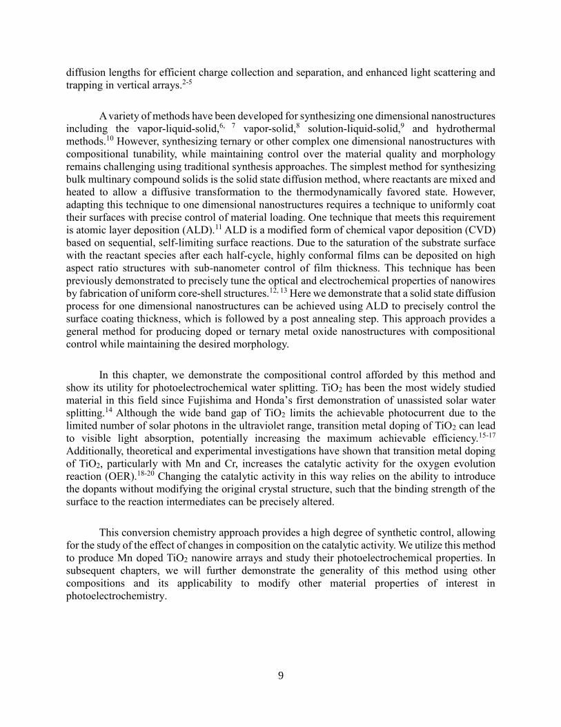
A novel method for atomic layer deposition (ALD) of manganese oxide was developed
using a bis(isopropylacetamidinate)manganese precursor and water vapor as co-reactants.
Previously reported work on ALD of manganese oxide has typically relied on cyclopentadienyl
precursors.23-25 Amidinates are well suited for use as ALD precursors due to their high volatility,
thermal stability, and reactivity, and have been successfully used for ALD and CVD of various
transition metals and transition metal oxides.26-28 To measure film thicknesses, ALD MnOx was
deposited on planar Si substrates and conformally coated on TiO2 nanowires yielding core-shell
nanowires. The film thicknesses on Si were measured using ellipsometry, and the thickness on the
nanowires was measured using transmission electron microscopy (TEM). Two important
characteristics of an ALD reaction are the saturation of the surface reaction after each precursor
pulse, and a linear relationship between film thickness and number of cycles after a sufficient
number of cycles.11 Saturating, linear growth was demonstrated indicating an ALD growth mode
(Fig 1). A growth rate of ~1Å/cycle was measured both on Si substrates and TiO2 nanowires, with
no thickness gradient along the nanowire length. Using X-ray photoelectron spectroscopy (XPS),
no measurable carbon or nitrogen was observed in the spectrum following a 1 min Ar sputtering
(Fig 1). Because the amidinate ligand contains carbon and nitrogen, the lack of any organic
contamination in the film indicates that the ALD surface reaction was complete, and the ligands
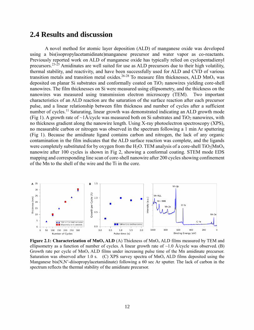
were completely substituted for by oxygen from the H2O. TEM analysis of a core-shell TiO2|MnOx
nanowire after 100 cycles is shown in Fig 2, showing a conformal coating. STEM mode EDS
mapping and corresponding line scan of core-shell nanowire after 200 cycles showing confinement
of the Mn to the shell of the wire and the Ti in the core.
Figure 2.1: Characterization of MnOx ALD (A) Thickness of MnOx ALD films measured by TEM and
ellipsometry as a function of number of cycles. A linear growth rate of ~1.0 Å/cycle was observed. (B)
Growth rate per cycle of MnOx ALD films under increasing pulse time of the Mn amidinate precursor.
Saturation was observed after 1.0 s. (C) XPS survey spectra of MnOx ALD films deposited using the
Manganese bis(N,N’-diisopropylacetamidinate) following a 60 sec Ar sputter. The lack of carbon in the
spectrum reflects the thermal stability of the amidinate precursor.
13
Figure 2.2: Core-shell nanowires produced by MnOx ALD (A) TEM image of a core-shell TiO2|MnOx
nanowire after 100 cycles, showing a conformal coating. Scale bar is 20 nm. (B,C) STEM mode EDS
mapping and corresponding line scan of core-shell nanowire after 200 cycles showing confinement of the
Mn to the shell of the wire and the Ti in the core. Scale bar is 100 nm.
Figure 2.3: Uniformly doped TiO2 nanowires using conversion chemistry approach (A,B) 45° and top
down SEM images of vertically aligned Mn:TiO2 nanowire array, scale bar is 1μm. (C) XRD pattern of
converted nanowires showing only peaks for rutile TiO2 and peaks corresponding to FTO substrate. Peaks
for rutile TiO2 are indicated. (D,E) TEM and HRTEM image of converted nanowire showing lattice spacing
consistent with rutile TiO2, scale bars are 100 and 2 nm, respectively. (F,G) STEM mode elemental maps
of Mn and Ti in converted wire showing homogeneous incorporation of dopant, scale bars are 20 nm. (H)
STEM mode elemental map of Mn and Ti in core-shell nanowire before annealing. Scale bar is 50 nm.
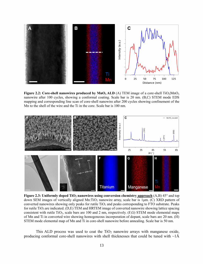
This ALD process was used to coat the TiO2 nanowire arrays with manganese oxide,
producing conformal core-shell nanowires with shell thicknesses that could be tuned with ~1Å
14
precision (Figure 3). The coated nanowire arrays were then annealed in an argon environment to
facilitate diffusion of the manganese atoms into the rutile lattice, yielding Mn doped TiO2
nanowires. The solid state diffusion process maintains the nanowire morphology as observed by
scanning electron microscopy (SEM) with an average nanowire diameter ~100 nm and length of
~1.5 µm (Figure 3a,b). Energy dispersive X-ray spectroscopy (EDS) confirms the presence of Mn
in the nanowire arrays and allows for quantification of the average Mn content as a function of
number of ALD cycles. The average composition of Mn in the nanowire arrays can be precisely
tuned by varying the shell thickness, and is in good agreement with calculated values for this
nanowire geometry. The concentration of Mn could not be extended above 10%, which is likely
due to the solubility limit of Mn in TiO2. XPS confirmed that the near surface composition of the
nanowires is similar to the average composition in the core. The X-ray diffraction (XRD) pattern
of the nanowire substrates after annealing only contains peaks corresponding to the rutile phase,
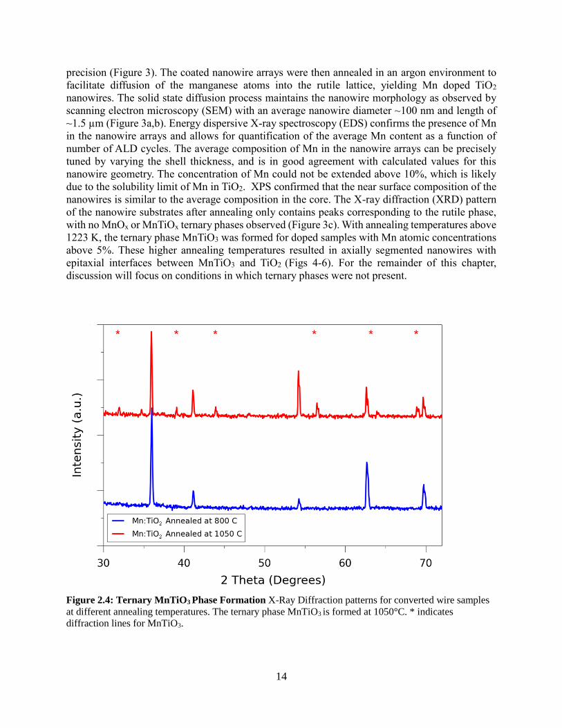
with no MnOx or MnTiOx ternary phases observed (Figure 3c). With annealing temperatures above
1223 K, the ternary phase MnTiO3 was formed for doped samples with Mn atomic concentrations
above 5%. These higher annealing temperatures resulted in axially segmented nanowires with
epitaxial interfaces between MnTiO3 and TiO2 (Figs 4-6). For the remainder of this chapter,
discussion will focus on conditions in which ternary phases were not present.
Figure 2.4: Ternary MnTiO3 Phase Formation X-Ray Diffraction patterns for converted wire samples
at different annealing temperatures. The ternary phase MnTiO3 is formed at 1050°C. * indicates
diffraction lines for MnTiO3.

15
Figure 2.5: Microstructure of ternary phase nanowires (A,B) TEM images of nanowires converted at
1050°C. Nanowires phase segregate to form axial segments of pure MnTiO3 and TiO2. Axial
segmentation is likely due to high diffusion rates of Mn2+ along c-axis. EDS confirms relative
stoichiometry of Mn and Ti in segments.
Figure 2.6: Interfaces of ternary phase nanowires (A,B) HRTEM images of nanowires converted at
1050°C, showing the interface between MnTiO3 and TiO2. (C-E) FFTs of TiO2 section, MnTiO3 section,
and interface respectively. (F) Moiré image shows epitaxial interface between MnTiO3 11̅0and TiO2 001
which can form due to the similarity of the oxygen sublattice in the two structures. However, edge
dislocations are observed at the interface.
To determine the distribution of the dopant atoms in the TiO2 nanowires and their effect of
the nanowire structure, the converted nanowires were further analyzed by TEM. TEM images of
16
Mn doped TiO2 nanowires show no sign of a MnOx shell after annealing, indicating that the
conversion process proceeded to completion. High resolution TEM (HRTEM) analysis was used
to investigate the microstructure of the doped nanowires and indicated that the nanowires remained
single crystalline after growth. Using HRTEM, we observed lattice spacing consistent with rutile
TiO2 with the nanowire growth axis parallel to the [001] direction. To obtain a visualization of the
distribution of the Mn atoms within the TiO2 lattice, Scanning TEM (STEM) mode EDS mapping
was conducted. The elemental maps show a homogeneous incorporation of the Mn atoms, in
contrast with the core-shell nanowire prior to annealing. Line scans across the diameter and length
of the wire before and after annealing showed the conversion of the core-shell geometry into a
homogeneous doped nanowire. The generality of the conversion chemistry approach will be
discussed in subsequent chapters, as the method was also applied successfully to synthesize Ta
doped TiO2 using ALD of Ta2O5 as a dopant source. No signal from Sn or F was observed by EDS
in any of the nanowires tested. The results of the TEM and XRD analyses suggest that this
conversion process allows for controlled homogeneous doping of the TiO2 nanowires while
maintaining the original crystal structure.
From single crystal studies on metal ion diffusion in rutile TiO2, the mechanism of
diffusion is suggested to be dependent on the charge state of the ion.29 Divalent impurity ions
diffuse rapidly along open channels parallel to the c-axis and are pushed into substitutional Ti
sites by interstitial Ti ions. Divalent ions therefore have a large anisotropy in diffusion
coefficient for different crystallographic directions. Trivalent and tetravalent ions dissolve
substitutionally and diffuse interstitially. Both mechanisms are important for mixed-valent
impurity ions such as Mn. However, in this system, the concentration gradient exists in the radial
direction, orthogonal to the c-axis. Therefore it is likely that the diffusion of Mn from the shell
into the wire core is driven by Mn atoms dissolving substitutionally and diffusing through an
interstitial mechanism. The larger diffusion coefficients observed for conversion in an Ar
environment are a result of changes in point defect concentrations, namely oxygen vacancies and
interstitial Ti atoms, with partial pressure of oxygen.
The transient diffusion of Mn in the TiO2 nanowire can be described mathematically by
Fick’s Second Law:
𝜕𝑐𝐴𝜕𝑡
= 𝐷𝐴𝐵𝜕2𝑐𝐴𝜕𝑥2
Where 𝑐𝐴 is the concentration of Mn and x is the distance from the edge of the nanowire.
The solution for diffusion into a finite medium solution can be obtained numerically and is
available in for simple geometric shapes in Gurney-Lurie charts. The numerical solution would
predict a more rapid conversion than the solution for a semi-infinite medium but otherwise
similar diffusion profiles. Therefore as a simple approximation, the nanowire can be considered a
semi-infinite medium to yield an analytical solution:
𝑐𝐴𝑠 − 𝑐𝐴𝑐𝐴𝑠 − 𝑐𝐴0
= erf(𝑧
2√𝐷𝐴𝐵𝑡)
The surface concentration of Mn (𝑐𝐴𝑠)can be taken as unity as the nanowire shell is
manganese oxide. The initial concentration of Mn in the nanowire (𝑐𝐴0) is zero. From single

17
crystal studies the diffusion coefficients of various transition metals in rutile TiO2 at different
partial pressures of oxygen are known.29 The diffusion coefficients of interest here are those
orthogonal to the c-axis, which are lower than those parallel to the c-axis. The diffusion
coefficients were also measured to be substantially higher at low partial pressures of oxygen. The
diffusion coefficient of Mn in TiO2 is quite high: 1.1*10-10 cm2/s at 900°C in air. As the diffusion
distance is quite small as the nanowire diameter is ~100 nm, the nanowires readily become fully
converted at high temperature.
To observe the transient diffusion behavior the conversion process was investigated at
lower temperatures. The expected distribution of Mn for the semi-infinite medium solution at
T=600°C is shown in Figure 7, assuming a diffusion coefficient of 2.7*10-12 cm2/s for Mn
diffusion orthogonal to the c-axis in an Ar environment. STEM elemental maps for incomplete
conversion for different conversion times are shown in Figure 8. We see that at elevated
temperatures the conversion is very rapid, and that the expected diffusion profiles are reproduced
by the experimental data.
Figure 2.7: Calculated transient diffusion of Mn in TiO2 nanowires Mn distributions in the TiO2
nanowire as a function of time for conversion at 600°C in an Ar environment. The nanowire is assumed to
be a semi-infinite medium. The nanowire becomes fully converted in a relatively short conversion time.
Figure 2.8: Characterization of transient diffusion of Mn in TiO2 nanowires (A-D) STEM mode EDS
elemental maps for transient conversion of nanowire after 0, 1, 10, and 100 min of conversion at 600°C in
Ar.
18
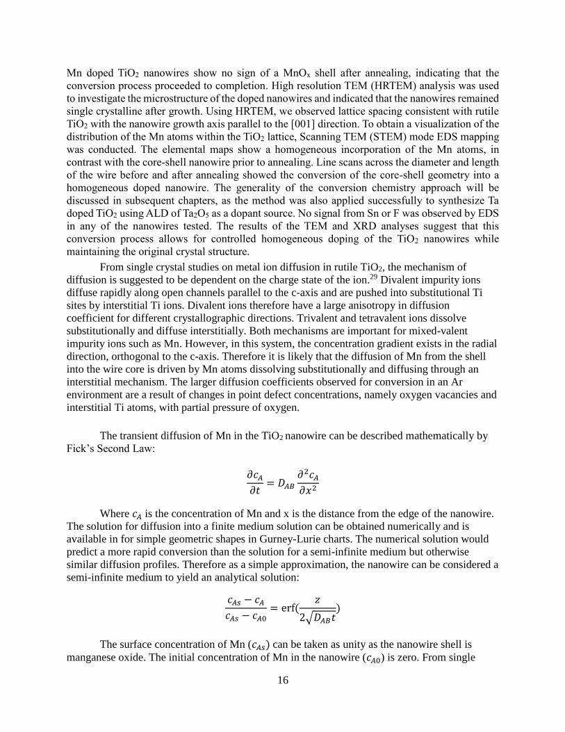
For further insight into the chemical environment and oxidation state of the Mn dopant
atoms within the TiO2 lattice, XPS and X-ray absorption spectroscopy (XANES, EXAFS) were
used. XPS was used to study the oxidation state of Mn before and after the conversion process.
Assignment of the oxidation state of Mn is not generally possible from the photoelectron peak
positions alone, as the binding energies for different oxidation states are quite similar. However,
previous studies have shown that comparison of the relative peak position of the 2p1/2 satellite to
its parent peak and the magnitude of the 3s multiplet splitting can be used to determine the
oxidation state of manganese.30-32 The Mn2+ oxidation state has a clear satellite peak approximately
6 eV from the parent 2p1/2 which is absent in the higher oxidation states. Oxides in the higher
oxidation states have a weaker peak near 10-11 eV from the 2p1/2 peak. The multiplet splitting of
the 3s peak is also dependent on the oxidation state. An increased oxidation state corresponds to
fewer unpaired 3p electrons, leading to a weaker coupling with the unpaired core-level electron
formed in the photoionization process, which results in a smaller multiplet splitting. The as
deposited film was found to have a Δ2p1/2 of 10.75 eV and a Δ3s of 5.7 eV indicating an average
oxidation state between Mn3+ and Mn4+ as seen in Figure 9. As the metallorganic precursor contains
Mn2+ cations and surface oxidation of MnO is well known, it is possible that the ALD film deposits
in a lower oxidation state and is oxidized in ambient conditions. After annealing, the Δ2p1/2 was
reduced to 6.2 eV and a Δ3s of 6.0 eV, matching that of the MnO phase. The annealing process
therefore reduces the Mn from a mixed Mn3+/4+ valence to a Mn2+ oxidation state, possibly due to
the formation of oxygen vacancies in the Ar environment. The Ti 2p region of the undoped and
doped samples was also investigated, and no change was observed in the binding energies or peak
structure.
19
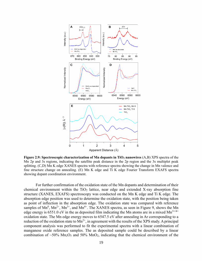
Figure 2.9: Spectroscopic characterization of Mn dopants in TiO2 nanowires (A,B) XPS spectra of the
Mn 2p and 3s regions, indicating the satellite peak distance in the 2p region and the 3s multiplet peak
splitting. (C,D) Mn K edge XANES spectra with reference spectra showing the change in Mn valence and
fine structure change on annealing. (E) Mn K edge and Ti K edge Fourier Transform EXAFS spectra
showing dopant coordination environment.
For further confirmation of the oxidation state of the Mn dopants and determination of their
chemical environment within the TiO2 lattice, near edge and extended X-ray absorption fine
structure (XANES, EXAFS) spectroscopy was conducted on the Mn K edge and Ti K edge. The
absorption edge position was used to determine the oxidation state, with the position being taken
as point of inflection in the absorption edge. The oxidation state was compared with reference
samples of Mn0, Mn2+, Mn3+, and Mn4+. The XANES spectra, as seen in Figure 9, shows the Mn
edge energy is 6551.0 eV in the as deposited film indicating the Mn atoms are in a mixed Mn3+/4+
oxidation state. The Mn edge energy moves to 6547.5 eV after annealing in Ar corresponding to a
reduction of the oxidation state to Mn2+, in agreement with the results of the XPS study. A principal
component analysis was performed to fit the experimental spectra with a linear combination of
manganese oxide reference samples. The as deposited sample could be described by a linear
combination of ~50% Mn2O3 and 50% MnO2, indicating that the chemical environment of the
A B
C D
E
20
manganese atoms in the as deposited sample is similar to that in the manganese oxide phases.
However, the fine structure of the annealed sample could not be reproduced by the reference
spectra, indicating the chemical environment of the Mn in the TiO2 lattice is quite different to that
of the manganese oxide phases, in accordance with the results of the XRD and TEM studies.
The Ti K edge EXAFS spectrum was taken for both the undoped and doped nanowire
samples. The nanowires have the rutile structure, in which each Ti atom is octahedrally coordinated
and bonded to 6 O atoms. The 6 O atoms are found at two distinct distances of 1.93 and 2.0 Å. The
next nearest paths are the Ti-Ti path between the Ti atom at the body center of a rectangular prism
and the eight Ti atoms occupying the vertices of the rectangular prism. The effect of the transition
metal substitution for Ti should be therefore be seen in the structure of the second and third peaks.
However, due to the low concentration of the dopant, the spectra are nearly unchanged, indicating
a preservation of the original rutile lattice and a chemical environment for the average Ti atom that
is not significantly perturbed by the presence of the Mn dopant. As it is assumed that Mn acts as a
substitutional dopant for Ti, the EXAFS spectrum of the dopant taken on the Mn K edge can be
qualitatively compared to the Ti K edge EXAFS spectrum, shown in Figure 9. The spectra show
clear similarities although the paths dominated by the Mn-O and Mn-Ti bonds appear longer,
indicating a structural distortion caused by the larger ionic radius of the Mn2+ ion. A fitting of the
experimental spectrum was performed using ab initio FEFF calculations, to extract quantitative
structural parameters.21, 22 The structure model used was a rutile cluster with the core atom being
replaced with Mn. This structural model provides a good fit to the experimental spectrum, and the
bond lengths are observed to be extended, with the Mn-O bonds being 2.03 and 2.15 Å, similar to
the Mn-O bond length seen in the Mn2+ oxide, and the Mn-Ti path being 3.30 Å.
To evaluate the impact of the Mn doping process on the properties of the nanowires,
electrochemical measurements were performed. The electrocatalytic activity of the nanowire
substrates for the OER was evaluated across the entire compositional range investigated using
cyclic voltammetry in a standard 3-electrode set-up. The relevant figure of merit used for
evaluation of electrocatalytic activity for solar water splitting devices is the overpotential required
to achieve a current density of 10 mA cm-2.33 The difference in catalytic activities between different
surfaces for the OER is determined by the O* adsorption energy.34 Rutile TiO2 lies on the right
side of the OER activity volcano, indicating the O* binding is too weak. The introduction of the
dopant leads to a stronger interaction between the adsorbate and the surface, resulting in a binding
energy nearer the maximum of the activity volcano. The ability to alter the composition while
maintaining the original crystal structure allows for access to intermediate binding energies
between those of the undoped surface and the dopant in its oxide phase.18 The overpotential was
reduced for all concentrations measured for the converted nanowire substrates (Figure 10a).

21
Figure 2.10: Electrochemical characterization of Mn doped TiO2 nanowires (A) Voltammograms of
OER activity for doped and undoped nanowire samples with overpotential required to achieve a benchmark
current density of 10 mA/cm-2 based on geometric surface area. 25x denotes a sample prepared from 25
cycles of MnOx ALD. (B) Short term stability test using controlled current electrolysis at 10 mA/cm-2 based
on geometric surface area. (C) UV-Visible absorption spectra of doped and undoped nanowire samples. (D)
Photoelectrochemical performance of undoped and doped nanowire samples using 50x Mn:TiO2.
The lowest overpotential was measured for Mn:TiO2 prepared from 50 cycles of ALD,
denoted 50x Mn:TiO2, corresponding to a doping concentration of ~6%, similar to the dopant
concentration used for the computational studies of Nørskov and coworkers.18 It is possible that at
higher Mn concentrations the surface becomes too strongly binding. The overpotential required
was 0.5 V, or a potential of 1.73 V versus the reversible hydrogen electrode. This value is
comparable to previously reported values of 1.77 V and 1.84 V for MnOx electrocatalysts and
~1.55-1.65 V for high performing electrodeposited catalysts.24, 33, 35 The improvement observed
here is also in agreement with previous studies on transition metal doped TiO2. The improvement
in activity for ~2% dopant concentration relative to the undoped TiO2 is comparable to that found
A
B
C D
22
by Liu et al, although the current density in the study was limited by the small electrochemically
accessible surface area of the submonolayer films.20 The short term stability of these samples was
measured using chronopotentiometry. The catalyst material was held at a constant current density
of 10 mA cm-2 per geometric area for 2 h while the potential needed to maintain this current density
was measured. (Figure 10b) The potential at 2 hours increased to ~1.8 V, indicating the catalyst is
relatively stable, in contrast to MnOx based catalysts, which form MnO4- soluble species and
dissolve in alkaline conditions and under large applied potentials.36
Historically, a variety of transition metals have been explored as dopants in modifying the
electronic structure of TiO2 to improve its visible light photocatalytic activity.15-17 Previous
theoretical studies show that doping TiO2 with manganese introduces an occupied mid gap state
which is very localized and primarily comprised of the Mn t2g orbitals. The visible light absorption
in this material is a charge transfer from the dopant mid gap state to the conduction band or an
acceptor transition from the valence band to the impurity band.15 We observe that the doped
samples are yellow-brown, departing from the white color of the undoped product. Consequently
the light absorption of the Mn doped TiO2 nanowires extends from the ultraviolet into the visible
range as an extended tail, potentially widening the usable range for photocarrier generation for
driving the water oxidation reaction. (Figure 10c) It is important to note that the band edge position
of the TiO2 is unchanged, indicating that the tail in the visible range derives mainly from low
energy excitations. The mid gap states introduced by the Mn impurity are predicted to be very
localized, with little carrier mobility, and could possibly act as recombination centers. The
photoelectrochemical performance of the doped TiO2 films was measured in a 3 electrode set up
under simulated solar illumination to determine the effect of the Mn dopant on the photoreactivity.
The maximum photocurrent achieved from the doped devices was found to be reduced relative to
that of the undoped devices, possibly indicating that the mid gap states formed by the transition
metal dopant are acting as recombination centers. (Figure 10d) Although the transition metal
doping process allows for visible light absorption, efficient charge collection is required to increase
the obtainable photocurrent. This conversion chemistry approach could potentially be applied in
such a way that the electronic structure of the light absorber is not negatively affected. This could
include the synthesis of ternary metal oxide light absorbers or doping in which the impurity band
formed connects with the valence or conduction band allowing for charge carrier extraction.
Additionally the ability to precisely tune the composition of mixed metal oxides while maintaining
a desired morphology has promise for the development of OER catalysts as demonstrated in this
work.
2.5 Conclusions
We have developed a simple and general synthetic method for rationally designing complex
metal oxide nanostructures, and demonstrated a novel process for atomic layer deposition of
manganese oxide. In this study, we show the utility of this method by investigating the
electrocatalytic, optical, and photoelectrochemical properties of Mn doped TiO2 nanowires as a
model system. The Mn dopants are homogeneously incorporated in the rutile TiO2 lattice without
the formation of extraneous crystalline phases. These nanowires show promising electrocatalytic
activity for water oxidation, but photoelectrochemical performance of the doped nanowire arrays
is negatively affected, possibly owing to the introduction of an impurity band in the band gap of
TiO2. We further demonstrate the generality of this method by extending it to a second

23
compositional system. Further studies could utilize this simple conversion chemistry approach to
investigate functional complex metal oxide nanostructures, such as ternary metal oxide light
absorbers or mixed metal oxides for water oxidation electrocatalysis.
2.6 References
1. Dasgupta, N. P.; Sun, J.; Liu, C.; Brittman, S.; Andrews, S. C.; Lim, J.; Gao, H.; Yan, R.;
Yang, P. Adv. Mater. 2014, 26, (14), 2137-2184.
2. Liu, C.; Dasgupta, N. P.; Yang, P. Chem. Mater. 2014, 26, (1), 415-422.
3. Warren, E. L.; Atwater, H. A.; Lewis, N. S. J. Phys. Chem. C 2014, 118, (2), 747-759.
4. Liu, C.; Tang, J.; Chen, H. M.; Liu, B.; Yang, P. Nano Lett. 2013, 13, (6), 2989-2992.
5. Boettcher, S. W.; Spurgeon, J. M.; Putnam, M. C.; Warren, E. L.; Turner-Evans, D. B.;
Kelzenberg, M. D.; Maiolo, J. R.; Atwater, H. A.; Lewis, N. S. Science 2010, 327, (5962), 185-
187.
6. Morales, A. M.; Lieber, C. M. Science 1998, 279, (5348), 208-211.
7. Wu, Y.; Yang, P. J. Am. Chem. Soc. 2001, 123, (13), 3165-3166.
8. Huang, M. H.; Wu, Y.; Feick, H.; Tran, N.; Weber, E.; Yang, P. Adv. Mater. 2001, 13,
(2), 113-116.
9. Trentler, T. J.; Hickman, K. M.; Goel, S. C.; Viano, A. M.; Gibbons, P. C.; Buhro, W. E.
Science 1995, 270, (5243), 1791-1794.
10. Liu, B.; Aydil, E. S. J. Am. Chem. Soc. 2009, 131, (11), 3985-3990.
11. George, S. M. Chem. Rev. 2010, 110, (1), 111-131.
12. Dasgupta, N. P.; Jung, H. J.; Trejo, O.; McDowell, M. T.; Hryciw, A.; Brongersma, M.;
Sinclair, R.; Prinz, F. B. Nano Lett. 2011, 11, (3), 934-940.
13. Dasgupta, N. P.; Liu, C.; Andrews, S.; Prinz, F. B.; Yang, P. J. Am. Chem. Soc. 2013,
135, (35), 12932-12935.
14. Fujishima, A.; Honda, K. Nature 1972, 238, 37.
15. Umebayashi, T.; Yamaki, T.; Itoh, H.; Asai, K. J. Phys. Chem. Solids 2002, 63, (10),
1909-1920.
16. Liu, G.; Wang, L.; Yang, H. G.; Cheng, H.-M.; Lu, G. Q. J. Mater. Chem. 2010, 20, (5),
831-843.
17. Choi, W.; Termin, A.; Hoffmann, M. R. J. Phys. Chem. 1994, 98, (51), 13669-13679.
18. García-Mota, M.; Vojvodic, A.; Metiu, H.; Man, I. C.; Su, H.-Y.; Rossmeisl, J.; Nørskov,
J. K. ChemCatChem 2011, 3, (10), 1607-1611.
19. García-Mota, M.; Vojvodic, A.; Abild-Pedersen, F.; Nørskov, J. K. J. Phys. Chem. C
2013, 117, (1), 460-465.
20. Liu, B.; Chen, H. M.; Liu, C.; Andrews, S. C.; Hahn, C.; Yang, P. J. Am. Chem. Soc.
2013, 135, (27), 9995-9998.
21. Newville, M. J. Synchrotron Radiat. 2001, 8, (2), 322-324.
22. Rehr, J. J.; Albers, R. C. Rev. Mod. Phys. 2000, 72, (3), 621-654.
23. Burton, B. B.; Fabreguette, F. H.; George, S. M. Thin Solid Films 2009, 517, (19), 5658-
5665.
24. Pickrahn, K. L.; Park, S. W.; Gorlin, Y.; Lee, H.-B.-R.; Jaramillo, T. F.; Bent, S. F. Adv.
Energy Mater. 2012, 2, (10), 1269-1277.
24
25. Strandwitz, N. C.; Comstock, D. J.; Grimm, R. L.; Nichols-Nielander, A. C.; Elam, J.;
Lewis, N. S. J. Phys. Chem. C 2013, 117, (10), 4931-4936.
26. Lim, B. S.; Rahtu, A.; Park, J.-S.; Gordon, R. G. Inorg. Chem. 2003, 42, (24), 7951-7958.
27. Lim, B. S.; Rahtu, A.; Gordon, R. G. Nat. Mater. 2003, 2, 749.
28. Au, Y.; Lin, Y.; Kim, H.; Beh, E.; Liu, Y.; Gordon, R. G. J. Electrochem. Soc. 2010, 157,
(6), D341-D345.
29. Sasaki, J.; Peterson, N. L.; Hoshino, K. J. Phys. Chem. Solids 1985, 46, (11), 1267-1283.
30. Oku, M.; Hirokawa, K.; Ikeda, S. J. Electron Spectrosc. Relat. Phenom. 1975, 7, (5),
465-473.
31. Di Castro, V.; Polzonetti, G. J. Electron Spectrosc. Relat. Phenom. 1989, 48, (1), 117-
123.
32. Gorlin, Y.; Jaramillo, T. F. ECS Trans. 2011, 41, (1), 1701-1707.
33. McCrory, C. C. L.; Jung, S.; Peters, J. C.; Jaramillo, T. F. J. Am. Chem. Soc. 2013, 135,
(45), 16977-16987.
34. Man, I. C.; Su, H.-Y.; Calle-Vallejo, F.; Hansen, H. A.; Martínez, J. I.; Inoglu, N. G.;
Kitchin, J.; Jaramillo, T. F.; Nørskov, J. K.; Rossmeisl, J. ChemCatChem 2011, 3, (7), 1159-
1165.
35. Gorlin, Y.; Jaramillo, T. F. J. Am. Chem. Soc. 2010, 132, (39), 13612-13614.
36. Su, H.-Y.; Gorlin, Y.; Man, I. C.; Calle-Vallejo, F.; Norskov, J. K.; Jaramillo, T. F.;
Rossmeisl, J. Phys. Chem. Chem. Phys. 2012, 14, (40), 14010-14022.

25
Chapter 3
TiO2|BiVO4 Nanowire Heterostructure
Photoanodes based on Type II Band
Alignment This chapter contains material from the following publication:
Resasco, J.; Zhang, H.; Kornienko, N.; Becknell, N.; Lee, H.; Guo, J.; Briseno, A.L.; Yang, P.
ACS Cent. Sci. 2016, 2, 80-88.
3.1 Abstract
Metal oxides that absorb visible light are attractive for use as photoanodes in
photoelectrosynthetic cells. However, their performance is often limited by poor charge carrier
transport. We show that this problem can be addressed by using separate materials for light
absorption and carrier transport. Here, we report a Ta:TiO2|BiVO4 nanowire photoanode, in
which BiVO4 acts as a visible light-absorber and Ta:TiO2 acts as a high surface area electron
conductor. Electrochemical and spectroscopic measurements provide experimental evidence for
the type II band alignment necessary for favorable electron transfer from BiVO4 to TiO2. The
host−guest nanowire architecture presented here allows for simultaneously high light absorption
and carrier collection efficiency, with an onset of anodic photocurrent near 0.2 V vs RHE, and a
photocurrent density of 2.1 mA/cm2 at 1.23 V vs RHE.
3.2 Introduction
Harnessing energy from sunlight is a means of meeting the large global energy demand in
a cost effective and environmentally benign manner. However, to provide constant and stable
power on demand, it is necessary to convert sunlight into an energy storage medium.1 An example
of such a method is the production of hydrogen by photoelectrochemical (PEC) water splitting.
The direct splitting of water can be achieved using a single semiconductor, however, due to the
voltage requirement of the water splitting reaction and the associated kinetic overpotentials, only

26
wide band-gap materials can perform overall water splitting, limiting the efficiency due to
insufficient light absorption.2 To address this issue, a dual-band-gap z-scheme system can be
utilized, with a semiconductor photoanode and photocathode to perform the respective oxidation
and reduction reactions.3 This approach allows for the use of lower-band-gap materials that can
absorb complementary portions of the solar spectrum and yield higher solar-to-fuel efficiencies.4,
5 In this integrated system, the charge flux is matched in both light absorbers of the
photoelectrochemical cell. Therefore, the overall performance is determined by the limiting
component. In most photoelectro-synthetic cells, this limiting component is the semiconductor
photoanode.6
Metal oxides have been heavily researched as photoanode materials since few conventional
light absorber materials are stable at the highly oxidizing conditions required for water oxidation.7
However, the most commonly studied binary oxide, TiO2, has a band-gap that is too large to absorb
sunlight efficiently (∼3.0 eV), consequently limiting its achievable photocurrent.8 While
promising work has recently been done on stabilizing conventional light absorbers such as Si,9
GaAs,10 and InP,11 the photovoltage obtained by these materials thus far has been insufficient to
match with smaller band gap photocathode materials such as Si and InP in a dual absorber
photoelectro-synthetic cell.12, 13 Additionally, these materials have high production and processing
costs. Small band gap metal oxides that absorb visible light and can be inexpensively synthesized,
such as WO3, Fe2O3, and BiVO4, are alternative materials that hold promise to overcome these
limitations.14-16 Among these metal oxides, BiVO4 has emerged as one of the most promising
materials due to its relatively small optical band gap of ~2.5 eV and its negative conduction band
edge (∼0 V versus RHE).17, 18 Under Air-Mass 1.5 Global (AM1.5G) solar illumination, the
maximum achievable photocurrent for water oxidation using BiVO4 is ~7 mA/cm2.16 However,
the water oxidation photocurrent obtained in practice for BiVO4 is substantially lower than this
value, mainly due to poor carrier transport properties, with electron diffusion lengths shorter than
the film thickness necessary to absorb a substantial fraction of light.17
One approach for addressing this problem is to use two separate materials for the tasks of
light absorption and carrier transport. To maximize performance, a conductive and high surface
area support material (“host”) is used, which is coated with a highly dispersed visible light absorber
(“guest”). This architecture allows for efficient use of absorbed photons due to the proximity of
the semiconductor liquid junction (SCLJ). This strategy has been employed in dye sensitized
(DSSC) and quantum dot sensitized solar cells (QDSSC).19, 20 Using a host-guest scheme can
improve the performance of photoabsorbing materials with poor carrier transport but relies upon
appropriate band alignment between the host and guest. Namely, the electron affinity of the host
should be larger, to favor electron transfer from guest to host without causing a significant loss in
open-circuit voltage.21 Nanowire arrays provide several advantages for use as the host material as
they allow high surface area loading of the guest material, enhanced light scattering for improved
absorption, and one-dimensional electron transport to the back electrode.22 Therefore, nanowire
arrays have been used as host materials in DSSCs, QDSSCs, and hybrid perovskite solar cells.23-
25 In photoelectro-synthetic cells, host-guest architectures have been utilized for oxide
photoanodes such as Fe2O3|TiSi2,26 Fe2O3|WO3,
27 Fe2O3|SnO2,28 and Fe2TiO5|TiO2.
29 For BiVO4,
it has been studied primarily with WO3|BiVO4 30-32, ZnO|BiVO4
33, and anatase TiO2|BiVO4.34
While attractive for its electronic transport properties, ZnO is unstable in aqueous environments,
and WO3 has the disadvantage of having a relatively positive flatband potential (~0.4 V vs RHE)14

27
resulting in potential energy losses for electrons as they are transferred from BiVO4 to WO3,
thereby limiting the photovoltage of the combined system. Performance in the low potential region
is critical for obtaining high efficiency in photoelectrosynthetic cells when coupled to typical p-
type photocathode materials such as Si or InP.12, 13 TiO2 is both stable in a wide range of pH and
has a relatively negative flat band potential (~0.2 V vs RHE)7 which does not significantly limit
the photovoltage obtainable from BiVO4, while still providing a driving force for electron transfer.
While TiO2 has intrinsically low mobility, doping TiO2 with donor type defects could increase the
carrier concentration and thus the conductivity. Indeed, niobium and tantalum doped TiO2 have
recently been investigated as potential transparent conductive oxide (TCO) materials.35, 36 A host
material with high carrier concentration could also ensure low contact resistance with the guest
material.37
Using a solid state diffusion approach based on atomic layer deposition (ALD), we have
previously demonstrated the ability to controllably and uniformly dope TiO2.38 In this study we
demonstrate a host-guest approach using Ta-doped TiO2 (Ta:TiO2) nanowires as a host and BiVO4
as a guest material. This host-guest nanowire architecture allows for simultaneously high light
absorption and carrier collection efficiency, with an onset of anodic photocurrent near 0.2 V vs
RHE, and a photocurrent of 2.1 mA/cm2 at 1.23 V vs RHE. We show that the synergistic effect of
the host-guest structure results in higher performance than either pure TiO2 or BiVO4. We also
experimentally demonstrate thermodynamically favorable band alignment between TiO2 and
BiVO4 using spectroscopic and electrochemical methods, and study the band edge electronic
structure of the TiO2 and BiVO4 using X-ray absorption and emission spectroscopies.
3.3 Experimental methods
3.3.1 Synthesis of titanium dioxide nanowire arrays
Similarly to discussed in Chapter 2, titanium dioxide (TiO2) nanowires were synthesized
by a hydrothermal method.39 In a typical synthesis, 83 μL of titanium isopropoxide was mixed
with 5 mL of 6M hydrochloric acid in a 40 mL Teflon vessel. A fluorine-doped tin oxide (FTO)
coated glass substrate was angled against the wall of the Teflon vessel such that the FTO surface
was facing down. The Teflon vessel was loaded in a stainless steel autoclave and heated to 180°C
for 180 min. After cooling, the substrates were thoroughly rinsed in deionized water. Following
growth, the substrates were annealed in a tube furnace in air at 450°C for 30 min following a 30
min ramp from room temperature. The substrates were allowed to cool, after which a 20 nm TiO2
layer was deposited on the nanowire arrays by ALD.
3.3.2 Atomic layer deposition
Deposition of Ta2O5 thin films was performed in a customized thermal ALD reactor. The
precursors used for Ta2O5 deposition were pentakis(dimethylamido)tantalum (Strem purity 99%)
and water.40 The tantalum precursor was held in a stainless steel cylinder, which was maintained
at 105 °C. The water source was maintained at room temperature. The substrate temperature for
Ta2O5 deposition was 150°C. Typical pulse times for the tantalum precursor and water were 2.0
and 1.0 sec, respectively. The precursors used for TiO2 deposition were titanium(IV)chloride and
28
water. The titanium precursor and the water source were both maintained at room temperature.
The substrate temperature for TiO2 deposition was 300°C. Typical pulse times for the titanium
precursor and water were 0.2 and 0.1 sec, respectively. Nitrogen was used as a carrier and purge
gas in both processes at a flow rate of 10 sccm.
3.3.3 Conversion process
Similarly to discussed in Chapter 2, after the ALD process, the nanowire substrates were
loaded into the center of a 1-inch diameter quartz tube and heated in a tube furnace under an Ar
atmosphere at 823 K for 12 hrs.38
3.3.4 Synthesis of bismuth vanadate
A home-built thermal evaporation system was used to deposit varying amounts of Bi
metal as measured by the film thickness of evaporated metal incident on a quartz crystal monitor.
To convert the Bi metal to BiVO4, ~50 μL/cm2 of dimethyl sulfoxide (DMSO) containing 150
mM vanadyl acetylacetonate (VO(C5H7O2)2) was dropcast onto the Bi coated TiO2 samples to
fully cover their surface. The samples were then heated to 450 °C for 2 h in air following a ramp
from room temperature at a rate of ~1.8 °C/min. During heating, Bi metal and VO2+ ions oxidize
and react to form BiVO4. An excess of the vanadium source is used to ensure complete
conversion of Bi to BiVO4. Excess V2O5 formed during heating can be removed by soaking
samples in 1 M KOH solution for 30 min.41
3.3.5 Physical and chemical characterization
The morphology of the nanowire substrates was studied using scanning electron
microscopy. SEM images were collected using a Zeiss Gemini Ultra-55 Analytical Field Emission
Scanning Electron Microscope operating at 10 kV. Phase information was obtained using XRD.
XRD patterns were collected using a Bruker D8 Advance diffractometer with Cu Kα radiation.
Individual nanowires were imaged by transmission electron microscopy (TEM) using a JEOL
2100-F Field-Emission Analytical TEM operated at 200 kV equipped with an analytical pole piece,
a high solid-angle EDS system, and a HAADF (high-angle annular dark field) scanning TEM
(STEM) detector. Chemical information was investigated using X-ray photoelectron spectroscopy
(XPS). XPS spectra were collected using a PHI 5400 X-ray Photoelectron Spectrometer equipped
with a 4 kV Argon ion gun, with Al Kα radiation. The angle between the source and detector was
35°. The measurement chamber was maintained at ~10-9 torr during measurement, and
measurements were taken at a pass energy of 17.9 eV. All energies were calibrated to spurious
carbon at 284.6 eV. Ultraviolet photoelectron spectroscopy measurements were carried out on
Omicron SPHERA spectrometer with a He discharge lamp (He I line, 21.22 eV) as the excitation
source. To ensure the secondary electron cutoff was captured, a sample bias of −3 V was applied
to compensate for the instrument work function difference repelling low-kinetic energy electrons.
The base pressure of the analyzer chamber was below 6 × 10⁻⁹ torr. APXPS and XPS experiments
are performed at Beamline 9.3.2 of the Advanced Light Source, which employs a differentially
pumped electrostatic lens system that allows for measurements at pressures on the order of 100
mtorr.42 Unless otherwise noted, all photoelectron spectra were recorded at photon energies of 490
eV. XAS, XES, and RIXS measurements were performed at beamline 8.0.1 of the Advanced Light
Source (ALS) at Lawrence Berkeley National Laboratory (LBNL). Absorption data were collected
in total electron yield (TEY), total fluorescence yield (TFY), and partial fluorescence yield (PFY).

29
The resolution for XAS spectra was better than 0.15 eV at the O K-edge. The spectra were
normalized to the incident photon flux monitored by measuring the photocurrent from a clean gold
mesh. The instrumental resolution for X-ray emission was 0.4 eV, and the emission energy was
calibrated using the positions of the elastic features in the emission spectra.
3.3.6 Electrochemical characterization
Electrochemical properties of the nanowire samples were studied in a three-electrode
electrochemical cell using a Bio-Logic potentiostat/galvanostat with a built-in electrochemical
impedance spectroscopy (EIS) analyzer. Unless otherwise noted, all measurements were
performed at room temperature in 0.5 M potassium phosphate electrolyte buffered to pH 7, using
a platinum wire counter electrode and a Ag/AgCl reference electrode. The potential scale was
calibrated to a reversible hydrogen electrode. A 300-Watt Xe lamp equipped with an air mass
1.5G filter (Newport) was used as the light source. Prior to measurement, light intensity was
standardized using a calibrated silicon photodiode. For IPCE measurements, light from the xenon
lamp was dispersed by a monochromator (Newport Corp.), and the photocurrent was recorded at
a constant bias with a spectral step of 10 nm. The measured photocurrent was converted to IPCE
by normalizing to a standard photodiode with a known quantum efficiency.
3.4 Results and discussion
3.4.1 Development of a nanowire heterostructured photoanode
A schematic of the desired host-guest structure is shown in Figure 1, in which a high surface area
TiO2 nanowire array is used as an electron conductor, and small, highly dispersed BiVO4
nanoparticles coat the surface as visible light sensitizers. The small size of these nanoparticles
allows high collection efficiency of electrons by the nanowires, and the proximity of the
semiconductor liquid junction allows holes to reach the surface to perform the water oxidation
reaction. The Type II band alignment required for electron transfer between TiO2 and BiVO4 is
illustrated, in which electrons produced by photoexcitation in BiVO4 are transferred to the
conduction band of TiO2. Additionally, holes produced in TiO2 can move through the valence band
of BiVO4 and to the semiconductor surface to oxidize water. Scanning electron microscopy (SEM)
images of the as-grown nanowire arrays and the optimized Type II photoanode heterostructures
are shown in Figure 1b,c. The following sections discuss the development of these optimized
structures.
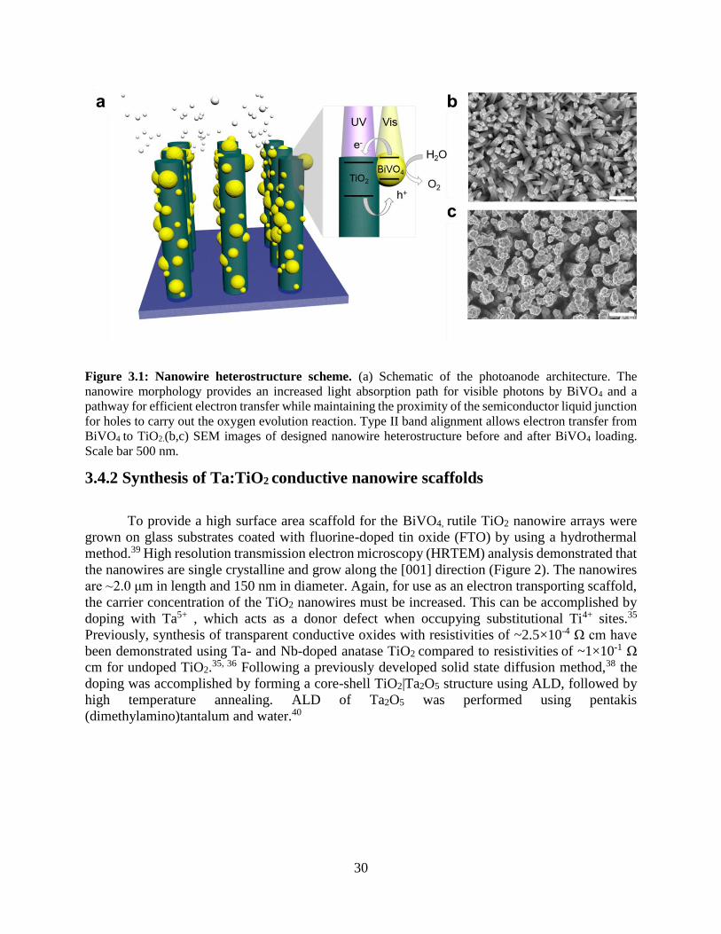
30
Figure 3.1: Nanowire heterostructure scheme. (a) Schematic of the photoanode architecture. The
nanowire morphology provides an increased light absorption path for visible photons by BiVO4 and a
pathway for efficient electron transfer while maintaining the proximity of the semiconductor liquid junction
for holes to carry out the oxygen evolution reaction. Type II band alignment allows electron transfer from
BiVO4 to TiO2.(b,c) SEM images of designed nanowire heterostructure before and after BiVO4 loading.
Scale bar 500 nm.
3.4.2 Synthesis of Ta:TiO2 conductive nanowire scaffolds
To provide a high surface area scaffold for the BiVO4, rutile TiO2 nanowire arrays were
grown on glass substrates coated with fluorine-doped tin oxide (FTO) by using a hydrothermal
method.39 High resolution transmission electron microscopy (HRTEM) analysis demonstrated that
the nanowires are single crystalline and grow along the [001] direction (Figure 2). The nanowires
are ~2.0 μm in length and 150 nm in diameter. Again, for use as an electron transporting scaffold,
the carrier concentration of the TiO2 nanowires must be increased. This can be accomplished by
doping with Ta5+ , which acts as a donor defect when occupying substitutional Ti4+ sites.35
Previously, synthesis of transparent conductive oxides with resistivities of ~2.5×10⁻⁴ Ω cm have
been demonstrated using Ta- and Nb-doped anatase TiO2 compared to resistivities of ~1×10⁻¹ Ω
cm for undoped TiO2.35, 36 Following a previously developed solid state diffusion method,38 the
doping was accomplished by forming a core-shell TiO2|Ta2O5 structure using ALD, followed by
high temperature annealing. ALD of Ta2O5 was performed using pentakis
(dimethylamino)tantalum and water.40
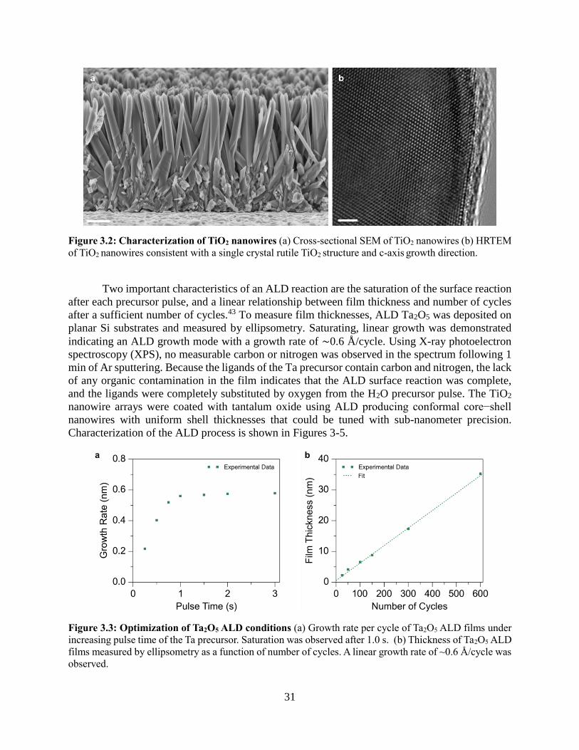
31
Figure 3.2: Characterization of TiO2 nanowires (a) Cross-sectional SEM of TiO2 nanowires (b) HRTEM
of TiO2 nanowires consistent with a single crystal rutile TiO2 structure and c-axis growth direction.
Two important characteristics of an ALD reaction are the saturation of the surface reaction
after each precursor pulse, and a linear relationship between film thickness and number of cycles
after a sufficient number of cycles.43 To measure film thicknesses, ALD Ta2O5 was deposited on
planar Si substrates and measured by ellipsometry. Saturating, linear growth was demonstrated
indicating an ALD growth mode with a growth rate of ∼0.6 Å/cycle. Using X-ray photoelectron
spectroscopy (XPS), no measurable carbon or nitrogen was observed in the spectrum following 1
min of Ar sputtering. Because the ligands of the Ta precursor contain carbon and nitrogen, the lack
of any organic contamination in the film indicates that the ALD surface reaction was complete,
and the ligands were completely substituted by oxygen from the H2O precursor pulse. The TiO2
nanowire arrays were coated with tantalum oxide using ALD producing conformal core−shell
nanowires with uniform shell thicknesses that could be tuned with sub-nanometer precision.
Characterization of the ALD process is shown in Figures 3-5.
Figure 3.3: Optimization of Ta2O5 ALD conditions (a) Growth rate per cycle of Ta2O5 ALD films under
increasing pulse time of the Ta precursor. Saturation was observed after 1.0 s. (b) Thickness of Ta2O5 ALD
films measured by ellipsometry as a function of number of cycles. A linear growth rate of ~0.6 Å/cycle was
observed.
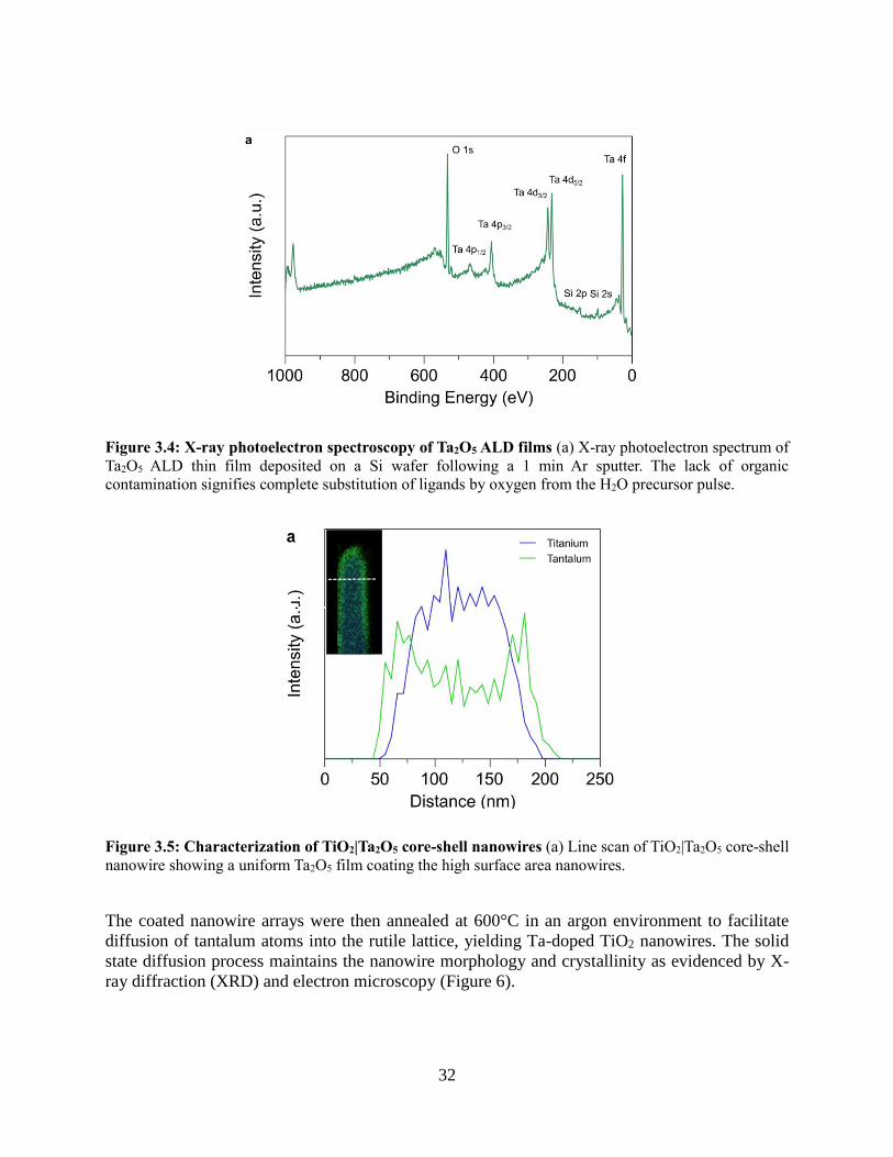
32
Figure 3.4: X-ray photoelectron spectroscopy of Ta2O5 ALD films (a) X-ray photoelectron spectrum of
Ta2O5 ALD thin film deposited on a Si wafer following a 1 min Ar sputter. The lack of organic
contamination signifies complete substitution of ligands by oxygen from the H2O precursor pulse.
Figure 3.5: Characterization of TiO2|Ta2O5 core-shell nanowires (a) Line scan of TiO2|Ta2O5 core-shell
nanowire showing a uniform Ta2O5 film coating the high surface area nanowires.
The coated nanowire arrays were then annealed at 600°C in an argon environment to facilitate
diffusion of tantalum atoms into the rutile lattice, yielding Ta-doped TiO2 nanowires. The solid
state diffusion process maintains the nanowire morphology and crystallinity as evidenced by X-
ray diffraction (XRD) and electron microscopy (Figure 6).
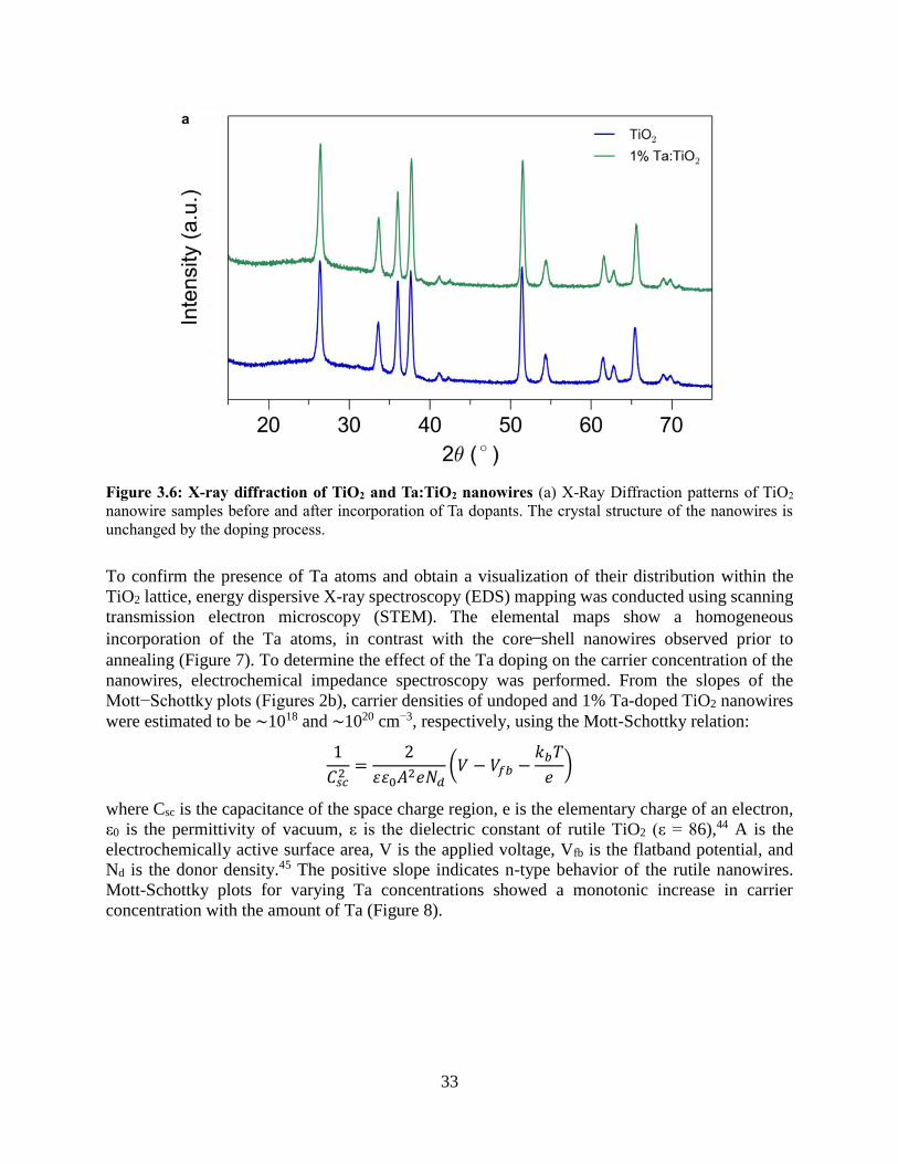
33
Figure 3.6: X-ray diffraction of TiO2 and Ta:TiO2 nanowires (a) X-Ray Diffraction patterns of TiO2
nanowire samples before and after incorporation of Ta dopants. The crystal structure of the nanowires is
unchanged by the doping process.
To confirm the presence of Ta atoms and obtain a visualization of their distribution within the
TiO2 lattice, energy dispersive X-ray spectroscopy (EDS) mapping was conducted using scanning
transmission electron microscopy (STEM). The elemental maps show a homogeneous
incorporation of the Ta atoms, in contrast with the core−shell nanowires observed prior to
annealing (Figure 7). To determine the effect of the Ta doping on the carrier concentration of the
nanowires, electrochemical impedance spectroscopy was performed. From the slopes of the
Mott−Schottky plots (Figures 2b), carrier densities of undoped and 1% Ta-doped TiO2 nanowires
were estimated to be ∼1018 and ∼1020 cm−3, respectively, using the Mott-Schottky relation:
1
𝐶𝑠𝑐2=
2
𝜀𝜀0𝐴2𝑒𝑁𝑑(𝑉 − 𝑉𝑓𝑏 −
𝑘𝑏𝑇
𝑒)
where Csc is the capacitance of the space charge region, e is the elementary charge of an electron,
ε0 is the permittivity of vacuum, ε is the dielectric constant of rutile TiO2 (ε = 86),44 A is the
electrochemically active surface area, V is the applied voltage, Vfb is the flatband potential, and
Nd is the donor density.45 The positive slope indicates n-type behavior of the rutile nanowires.
Mott-Schottky plots for varying Ta concentrations showed a monotonic increase in carrier
concentration with the amount of Ta (Figure 8).
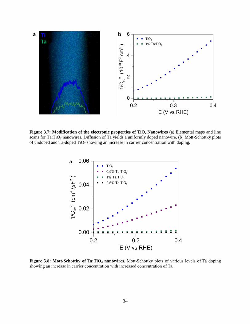
34
Figure 3.7: Modification of the electronic properties of TiO2 Nanowires (a) Elemental maps and line
scans for Ta:TiO2 nanowires. Diffusion of Ta yields a uniformly doped nanowire. (b) Mott-Schottky plots
of undoped and Ta-doped TiO2 showing an increase in carrier concentration with doping.
Figure 3.8: Mott-Schottky of Ta:TiO2 nanowires. Mott-Schottky plots of various levels of Ta doping
showing an increase in carrier concentration with increased concentration of Ta.
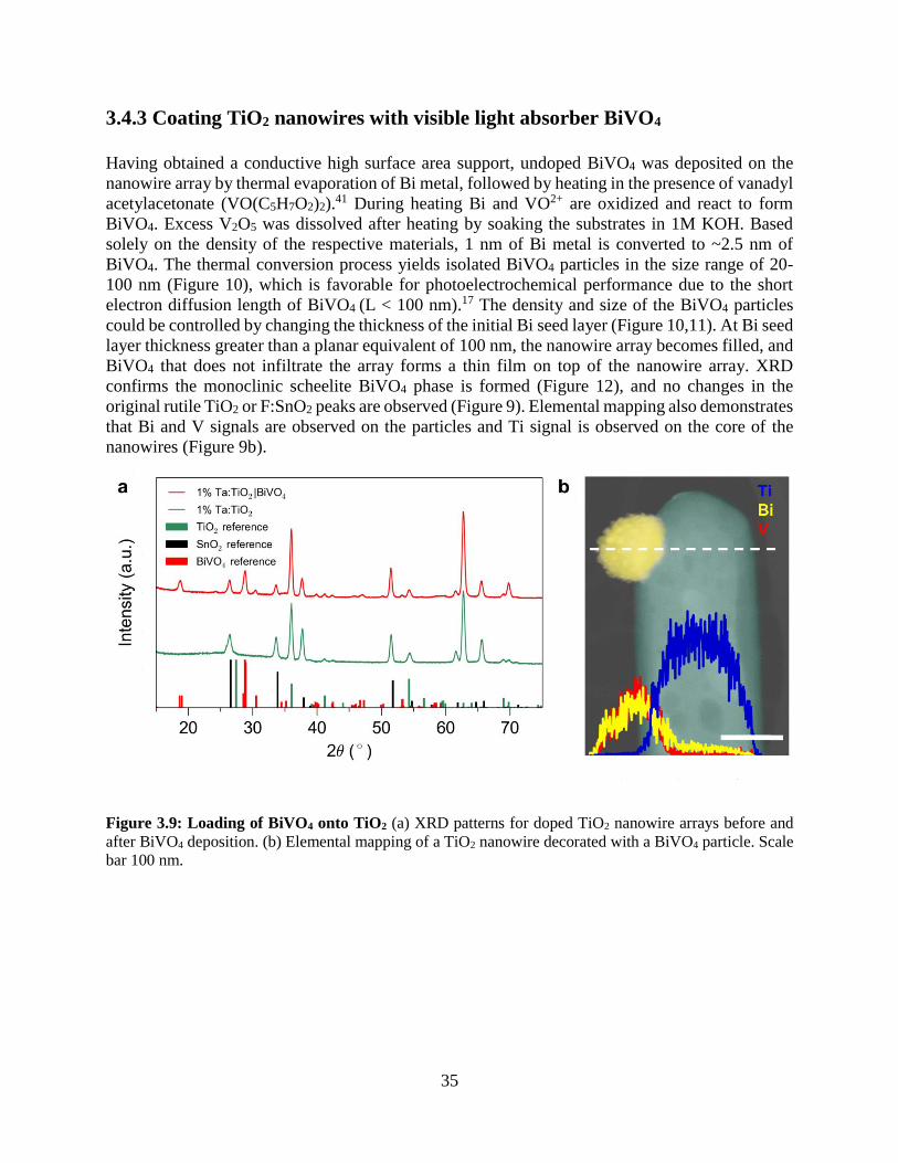
35
3.4.3 Coating TiO2 nanowires with visible light absorber BiVO4
Having obtained a conductive high surface area support, undoped BiVO4 was deposited on the
nanowire array by thermal evaporation of Bi metal, followed by heating in the presence of vanadyl
acetylacetonate (VO(C5H7O2)2).41 During heating Bi and VO2+ are oxidized and react to form
BiVO4. Excess V2O5 was dissolved after heating by soaking the substrates in 1M KOH. Based
solely on the density of the respective materials, 1 nm of Bi metal is converted to ~2.5 nm of
BiVO4. The thermal conversion process yields isolated BiVO4 particles in the size range of 20-
100 nm (Figure 10), which is favorable for photoelectrochemical performance due to the short
electron diffusion length of BiVO4 (L < 100 nm).17 The density and size of the BiVO4 particles
could be controlled by changing the thickness of the initial Bi seed layer (Figure 10,11). At Bi seed
layer thickness greater than a planar equivalent of 100 nm, the nanowire array becomes filled, and
BiVO4 that does not infiltrate the array forms a thin film on top of the nanowire array. XRD
confirms the monoclinic scheelite BiVO4 phase is formed (Figure 12), and no changes in the
original rutile TiO2 or F:SnO2 peaks are observed (Figure 9). Elemental mapping also demonstrates
that Bi and V signals are observed on the particles and Ti signal is observed on the core of the
nanowires (Figure 9b).
Figure 3.9: Loading of BiVO4 onto TiO2 (a) XRD patterns for doped TiO2 nanowire arrays before and
after BiVO4 deposition. (b) Elemental mapping of a TiO2 nanowire decorated with a BiVO4 particle. Scale
bar 100 nm.

36
Figure 3.10: Statistic of BiVO4 particle sizes on Ta:TiO2 nanowires (a,b) Particle size statistics and
representative SEM image of Ta:TiO2|BiVO4 sample with 100 nm Bi planar equivalent loading. Average
particle sizes for 25, 50, and 100 nm planar equivalents are 45 nm, 85 nm, and 148 nm, respectively. Scale
bar is 500 nm.
Figure 3.11: Statistics of BiVO4 particle sizes in thin films. (a) Particle size statistics for planar vs
nanowire loaded BiVO4. The nanowire array prevents large particle growth. (b) Representative SEM image
of a planar BiVO4 sample with 40 nm Bi planar equivalent loading. Average particle sizes for nanowire and
planar samples are 72 nm and 117 nm, respectively. Scale bar is 500 nm.
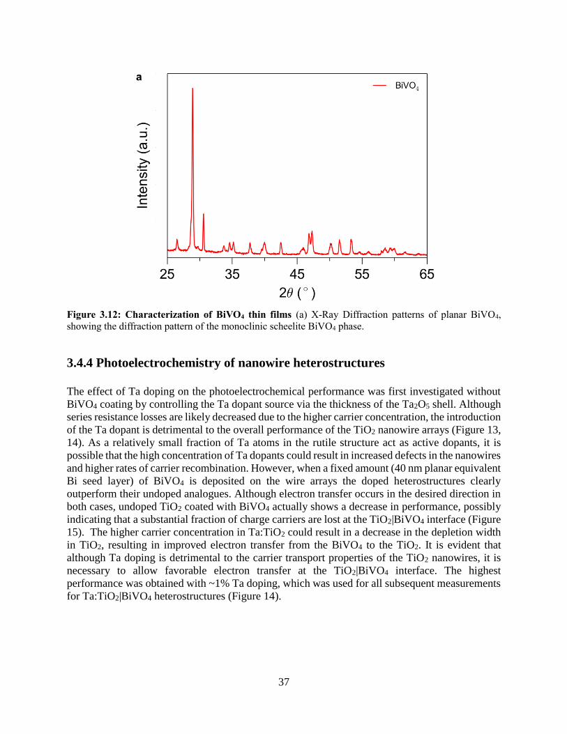
37
Figure 3.12: Characterization of BiVO4 thin films (a) X-Ray Diffraction patterns of planar BiVO4,
showing the diffraction pattern of the monoclinic scheelite BiVO4 phase.
3.4.4 Photoelectrochemistry of nanowire heterostructures
The effect of Ta doping on the photoelectrochemical performance was first investigated without
BiVO4 coating by controlling the Ta dopant source via the thickness of the Ta2O5 shell. Although
series resistance losses are likely decreased due to the higher carrier concentration, the introduction
of the Ta dopant is detrimental to the overall performance of the TiO2 nanowire arrays (Figure 13,
14). As a relatively small fraction of Ta atoms in the rutile structure act as active dopants, it is
possible that the high concentration of Ta dopants could result in increased defects in the nanowires
and higher rates of carrier recombination. However, when a fixed amount (40 nm planar equivalent
Bi seed layer) of BiVO4 is deposited on the wire arrays the doped heterostructures clearly
outperform their undoped analogues. Although electron transfer occurs in the desired direction in
both cases, undoped TiO2 coated with BiVO4 actually shows a decrease in performance, possibly
indicating that a substantial fraction of charge carriers are lost at the TiO2|BiVO4 interface (Figure
15). The higher carrier concentration in Ta:TiO2 could result in a decrease in the depletion width
in TiO2, resulting in improved electron transfer from the BiVO4 to the TiO2. It is evident that
although Ta doping is detrimental to the carrier transport properties of the TiO2 nanowires, it is
necessary to allow favorable electron transfer at the TiO2|BiVO4 interface. The highest
performance was obtained with ~1% Ta doping, which was used for all subsequent measurements
for Ta:TiO2|BiVO4 heterostructures (Figure 14).
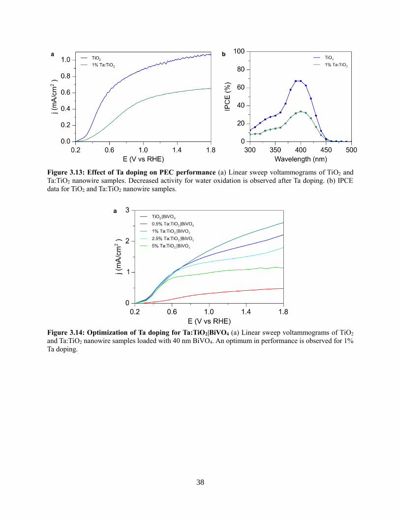
38
Figure 3.13: Effect of Ta doping on PEC performance (a) Linear sweep voltammograms of TiO2 and
Ta:TiO2 nanowire samples. Decreased activity for water oxidation is observed after Ta doping. (b) IPCE
data for TiO2 and Ta:TiO2 nanowire samples.
Figure 3.14: Optimization of Ta doping for Ta:TiO2|BiVO4 (a) Linear sweep voltammograms of TiO2
and Ta:TiO2 nanowire samples loaded with 40 nm BiVO4. An optimum in performance is observed for 1%
Ta doping.
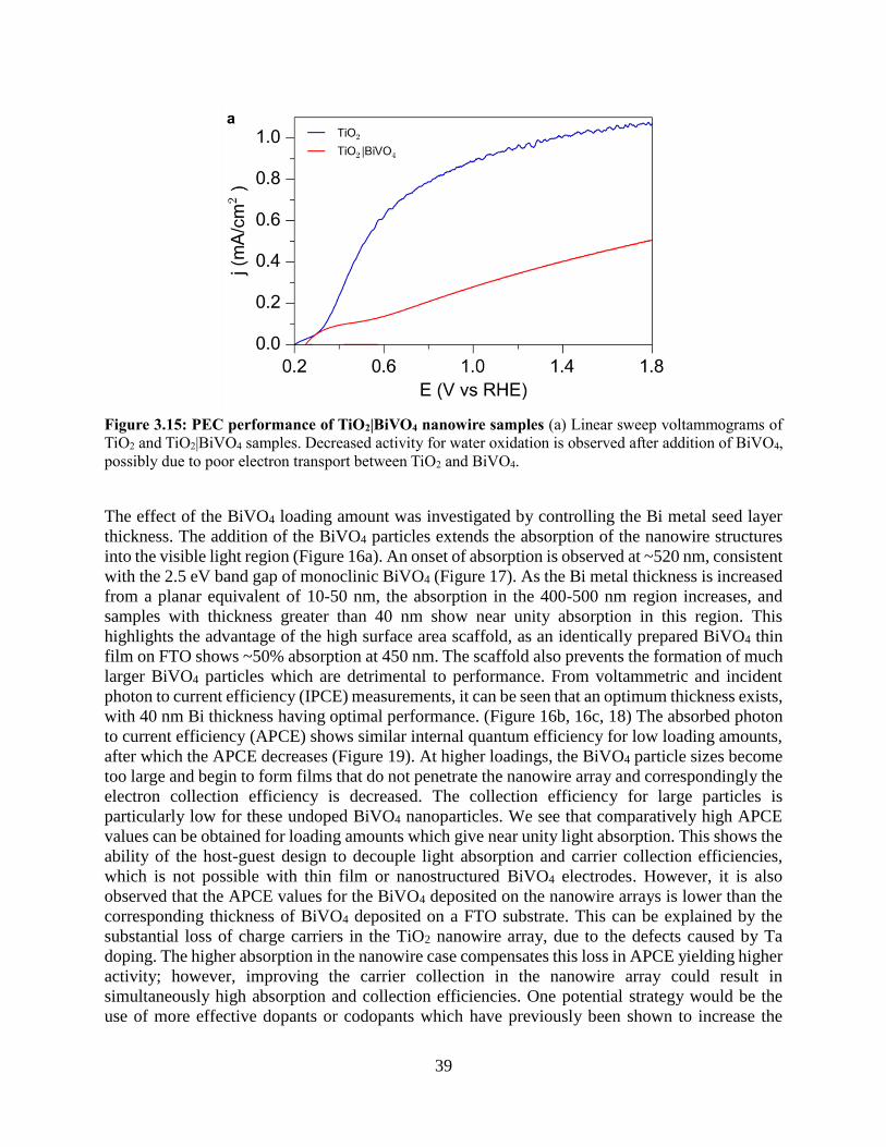
39
Figure 3.15: PEC performance of TiO2|BiVO4 nanowire samples (a) Linear sweep voltammograms of
TiO2 and TiO2|BiVO4 samples. Decreased activity for water oxidation is observed after addition of BiVO4,
possibly due to poor electron transport between TiO2 and BiVO4.
The effect of the BiVO4 loading amount was investigated by controlling the Bi metal seed layer
thickness. The addition of the BiVO4 particles extends the absorption of the nanowire structures
into the visible light region (Figure 16a). An onset of absorption is observed at ~520 nm, consistent
with the 2.5 eV band gap of monoclinic BiVO4 (Figure 17). As the Bi metal thickness is increased
from a planar equivalent of 10-50 nm, the absorption in the 400-500 nm region increases, and
samples with thickness greater than 40 nm show near unity absorption in this region. This
highlights the advantage of the high surface area scaffold, as an identically prepared BiVO4 thin
film on FTO shows ~50% absorption at 450 nm. The scaffold also prevents the formation of much
larger BiVO4 particles which are detrimental to performance. From voltammetric and incident
photon to current efficiency (IPCE) measurements, it can be seen that an optimum thickness exists,
with 40 nm Bi thickness having optimal performance. (Figure 16b, 16c, 18) The absorbed photon
to current efficiency (APCE) shows similar internal quantum efficiency for low loading amounts,
after which the APCE decreases (Figure 19). At higher loadings, the BiVO4 particle sizes become
too large and begin to form films that do not penetrate the nanowire array and correspondingly the
electron collection efficiency is decreased. The collection efficiency for large particles is
particularly low for these undoped BiVO4 nanoparticles. We see that comparatively high APCE
values can be obtained for loading amounts which give near unity light absorption. This shows the
ability of the host-guest design to decouple light absorption and carrier collection efficiencies,
which is not possible with thin film or nanostructured BiVO4 electrodes. However, it is also
observed that the APCE values for the BiVO4 deposited on the nanowire arrays is lower than the
corresponding thickness of BiVO4 deposited on a FTO substrate. This can be explained by the
substantial loss of charge carriers in the TiO2 nanowire array, due to the defects caused by Ta
doping. The higher absorption in the nanowire case compensates this loss in APCE yielding higher
activity; however, improving the carrier collection in the nanowire array could result in
simultaneously high absorption and collection efficiencies. One potential strategy would be the
use of more effective dopants or codopants which have previously been shown to increase the

40
carrier concentration of TiO2 nanowires without sacrificing performance.46, 47 Additionally, the
photoelectrochemical performance of the Ta:TiO2|BiVO4 nanowire photoanodes was investigated
in electrolyte containing sodium sulfite (Na2SO3), which acts as an efficient hole scavenger. As
the efficiency of hole capture by sulfite ions can be assumed to be near unity, measuring
photocurrent for sulfite oxidation allows for determination of the photoelectrochemical activity of
a photoanode irrespective of its water oxidation kinetics. It is clear that there is a significant
difference between the water oxidation and sulfite oxidation photocurrent (Figure 16d),
demonstrating that slow kinetics for water oxidation substantially limit the performance of the
photoanodes. To address this issue, a cobalt based catalyst was deposited on the Ta:TiO2|BiVO4
samples by photo-assisted electrodepostion.48 Cobalt oxides have also shown to have high activity
for water oxidation in near neutral pH with near unity charge transfer efficiencies.49-51 The
performance of the Ta:TiO2|BiVO4 electrodes before and after the deposition of the Co-Pi catalyst
are shown in Figure 16d. The performance is greatly enhanced, especially in the low potential
region, and the similarity with the performance to sulfite oxidation shows the efficiency of the
cobalt catalyst for decreasing surface recombination and improving water oxidation kinetics.
Figure 3.16: Photoelectrochemical performance of the Ta:TiO2/BiVO4 nanowire heterostructures
(a,b) Absorption and IPCE for Ta:TiO2|BiVO4 samples with increasing loading. Near complete absorption
and optimal activity is observed for planar equivalent thickness of 40 nm of Bi. (c) IPCE for Ta:TiO2 and
Ta:TiO2|BiVO4 showing visible contribution from BiVO4. (d) Current−voltage curves in 0.5 M potassium
phosphate electrolyte buffered to pH 7 with and without the presence of a hole scavenger. (b)
Current−voltage curves in 0.5 M potassium phosphate electrolyte buffered to pH 7 for Ta:TiO2 and
Ta:TiO2|BiVO4.
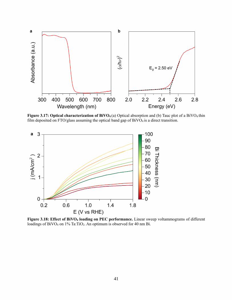
41
Figure 3.17: Optical characterization of BiVO4 (a) Optical absorption and (b) Tauc plot of a BiVO4 thin
film deposited on FTO/glass assuming the optical band gap of BiVO4 is a direct transition.
Figure 3.18: Effect of BiVO4 loading on PEC performance. Linear sweep voltammograms of different
loadings of BiVO4 on 1% Ta:TiO2. An optimum is observed for 40 nm Bi.
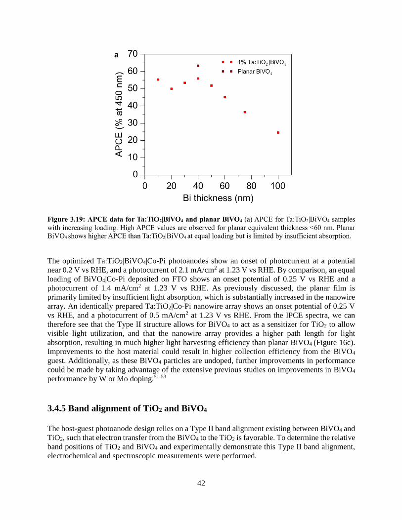
42
Figure 3.19: APCE data for Ta:TiO2|BiVO4 and planar BiVO4 (a) APCE for Ta:TiO2|BiVO4 samples
with increasing loading. High APCE values are observed for planar equivalent thickness <60 nm. Planar
BiVO4 shows higher APCE than Ta:TiO2|BiVO4 at equal loading but is limited by insufficient absorption.
The optimized Ta:TiO2|BiVO4|Co-Pi photoanodes show an onset of photocurrent at a potential
near 0.2 V vs RHE, and a photocurrent of 2.1 mA/cm2 at 1.23 V vs RHE. By comparison, an equal
loading of BiVO4|Co-Pi deposited on FTO shows an onset potential of 0.25 V vs RHE and a
photocurrent of 1.4 mA/cm2 at 1.23 V vs RHE. As previously discussed, the planar film is
primarily limited by insufficient light absorption, which is substantially increased in the nanowire
array. An identically prepared Ta:TiO2|Co-Pi nanowire array shows an onset potential of 0.25 V
vs RHE, and a photocurrent of 0.5 mA/cm2 at 1.23 V vs RHE. From the IPCE spectra, we can
therefore see that the Type II structure allows for BiVO4 to act as a sensitizer for TiO2 to allow
visible light utilization, and that the nanowire array provides a higher path length for light
absorption, resulting in much higher light harvesting efficiency than planar BiVO4 (Figure 16c).
Improvements to the host material could result in higher collection efficiency from the BiVO4
guest. Additionally, as these BiVO4 particles are undoped, further improvements in performance
could be made by taking advantage of the extensive previous studies on improvements in BiVO4
performance by W or Mo doping.51-53
3.4.5 Band alignment of TiO2 and BiVO4
The host-guest photoanode design relies on a Type II band alignment existing between BiVO4 and
TiO2, such that electron transfer from the BiVO4 to the TiO2 is favorable. To determine the relative
band positions of TiO2 and BiVO4 and experimentally demonstrate this Type II band alignment,
electrochemical and spectroscopic measurements were performed.

43
The flat band potential (Vfb) can give an estimate of the band positions of a semiconductor in an
aqueous environment. The primary method for determining Vfb is based on electrochemical
impedance spectroscopy and appears as the x-intercept of the linear portion of a Mott-Schottky
plot.45 In addition, the Vfb of a semiconductor will change as a function of pH due to surface
charging by adsorption of H+ and OH- ions. The Vfb was measured as a function of pH and shown
to change by approximately 59 mV/pH (Figure 20). Therefore, as shown in Figure 27a, the Vfbs of
TiO2 and BiVO4 are determined to be 0.19 V and 0.08 V vs. RHE, respectively. These results are
in agreement with previous measurements of the Vfb of the two semiconductors.17, 54 Assuming the
gap between the Vfb and the bottom edge of the conduction band is small (~0.2 eV) and similar for
TiO2 and BiVO4, this result is consistent with a Type II band alignment between the two
semiconductors.55
Figure 3.20: Mott-Schottky plots at varying pH for TiO2 and BiVO4 (a,b) Mott-Schottky plots for TiO2
and BiVO4. Efb is observed to shift ~59 mV/pH.
For further confirmation of the band positions, ultraviolet photoelectron spectroscopy (UPS) was
used in addition to Mott-Schottky measurements. UPS provides high energy resolution (<0.1 eV)
due to the small linewidth of the He discharge source and is therefore a powerful tool for
investigating the band positions of semiconductors. UPS allows one to obtain both the work
function of the material, which is the energetic difference between the photon energy of He I (21.22
eV) and the low kinetic energy cutoff of the spectrum, and the valence band maximum with respect
to the Fermi level (EF).56 The position of EF is referenced to a metal standard. The relationship
between these energy levels is depicted with the UPS spectrum of TiO2 and BiVO4 in Figure 27b.
Here, we are interested in the position of the band edges of the two semiconductors with respect
to the Evac. Thus we plot the spectra for TiO2 and BiVO4 with Evac at the same position. The
positions of the band edges are found using the Fermi level of a reference standard and linear
extrapolation of the valence band and secondary electron cutoff regions. The work functions for
TiO2 and BiVO4 were found to be 4.64 and 4.56 eV respectively, and the valence band positions
were found to be 7.61 and 6.99 eV vs the Evac, or 3.17 and 2.55 V on the RHE scale.

44
To give a complete picture of the band alignment of the two semiconductors, the conduction band
position was calculated by addition of the band gap to the valence band position. The optical band
gap of the two semiconductors was determined by constructing Tauc plots from optical absorption
data. (Figures 17, 21, 22). Extrapolation of the Tauc plot onto the x- intercept gives an optical band
gap of ~3.0 eV and ~2.5 eV for TiO2 and BiVO4, respectively (Figures 21, 22).57 Optical absorption
for TiO2 and Ta:TiO2 nanowires was identical (Figure 23). Additionally, the band gap was
confirmed by measuring the difference between the O-K edge X-ray emission and X-ray
absorption edge positions. This analysis yielded values of 2.5 and 3.0 eV, consistent with the
optical measurements (Figures 24, 25). Addition of the optical band gap to the valence band
position gives the conduction band position and completes the full band diagram (Figure 27c).
This analysis yielded conduction band values of 0.17 V vs RHE for TiO2 and 0.04 V vs RHE for
BiVO4. These spectroscopic measurements are consistent with the Type II band alignment between
TiO2 and BiVO4, and the electrochemical flat band potential measurements.
Figure 3.21: Tauc plot for BiVO4 for an indirect transition (a) Tauc plot of a BiVO4 thin film deposited
on FTO/glass assuming the optical band gap of BiVO4 is an indirect transition. A smaller band gap is
observed consistent with the work of Cooper et al.58

45
Figure 3.22: Optical characterization of TiO2 nanowires (a) Optical absorption and (b) Tauc plot of TiO2
nanowire samples on FTO/glass assuming the optical band gap of TiO2 is a direct transition.
Figure 3.23: UV Vis absorption for TiO2 and Ta:TiO2 nanowires (a) Optical absorption of TiO2 and
Ta:TiO2 nanowire samples demonstrating the optical absorption is not significantly changed by the doping
process.
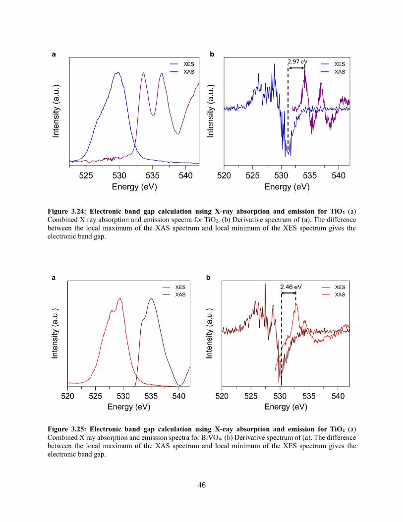
46
Figure 3.24: Electronic band gap calculation using X-ray absorption and emission for TiO2 (a)
Combined X ray absorption and emission spectra for TiO2. (b) Derivative spectrum of (a). The difference
between the local maximum of the XAS spectrum and local minimum of the XES spectrum gives the
electronic band gap.
Figure 3.25: Electronic band gap calculation using X-ray absorption and emission for TiO2 (a)
Combined X ray absorption and emission spectra for BiVO4. (b) Derivative spectrum of (a). The difference
between the local maximum of the XAS spectrum and local minimum of the XES spectrum gives the
electronic band gap.
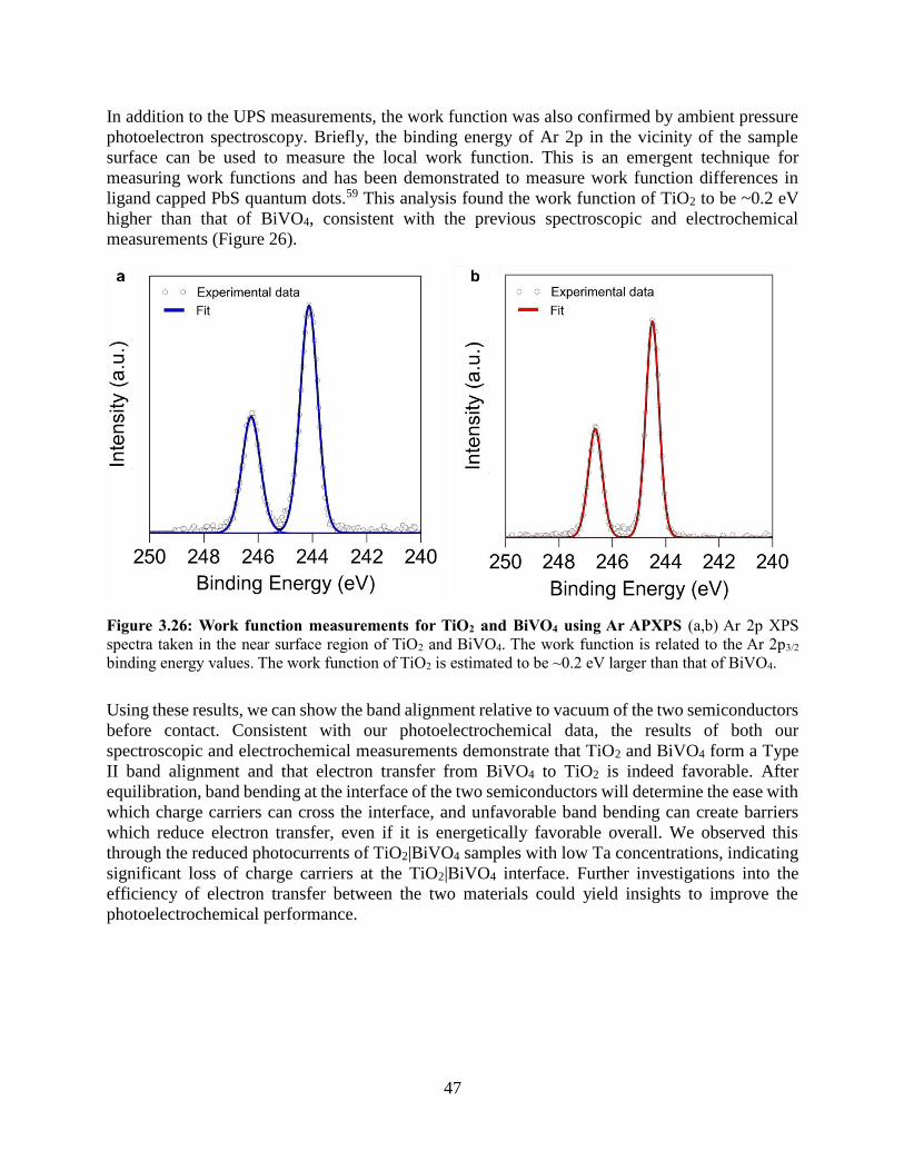
47
In addition to the UPS measurements, the work function was also confirmed by ambient pressure
photoelectron spectroscopy. Briefly, the binding energy of Ar 2p in the vicinity of the sample
surface can be used to measure the local work function. This is an emergent technique for
measuring work functions and has been demonstrated to measure work function differences in
ligand capped PbS quantum dots.59 This analysis found the work function of TiO2 to be ~0.2 eV
higher than that of BiVO4, consistent with the previous spectroscopic and electrochemical
measurements (Figure 26).
Figure 3.26: Work function measurements for TiO2 and BiVO4 using Ar APXPS (a,b) Ar 2p XPS
spectra taken in the near surface region of TiO2 and BiVO4. The work function is related to the Ar 2p3/2
binding energy values. The work function of TiO2 is estimated to be ~0.2 eV larger than that of BiVO4.
Using these results, we can show the band alignment relative to vacuum of the two semiconductors
before contact. Consistent with our photoelectrochemical data, the results of both our
spectroscopic and electrochemical measurements demonstrate that TiO2 and BiVO4 form a Type
II band alignment and that electron transfer from BiVO4 to TiO2 is indeed favorable. After
equilibration, band bending at the interface of the two semiconductors will determine the ease with
which charge carriers can cross the interface, and unfavorable band bending can create barriers
which reduce electron transfer, even if it is energetically favorable overall. We observed this
through the reduced photocurrents of TiO2|BiVO4 samples with low Ta concentrations, indicating
significant loss of charge carriers at the TiO2|BiVO4 interface. Further investigations into the
efficiency of electron transfer between the two materials could yield insights to improve the
photoelectrochemical performance.
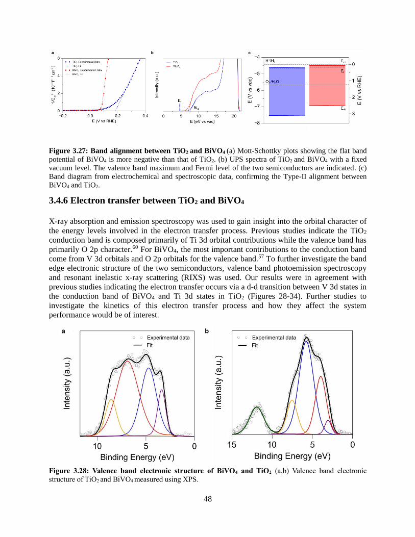
48
Figure 3.27: Band alignment between TiO2 and BiVO4 (a) Mott-Schottky plots showing the flat band
potential of BiVO4 is more negative than that of TiO2. (b) UPS spectra of TiO2 and BiVO4 with a fixed
vacuum level. The valence band maximum and Fermi level of the two semiconductors are indicated. (c)
Band diagram from electrochemical and spectroscopic data, confirming the Type-II alignment between
BiVO4 and TiO2.
3.4.6 Electron transfer between TiO2 and BiVO4
X-ray absorption and emission spectroscopy was used to gain insight into the orbital character of
the energy levels involved in the electron transfer process. Previous studies indicate the TiO2
conduction band is composed primarily of Ti 3d orbital contributions while the valence band has
primarily O 2p character.60 For BiVO4, the most important contributions to the conduction band
come from V 3d orbitals and O 2p orbitals for the valence band.57 To further investigate the band
edge electronic structure of the two semiconductors, valence band photoemission spectroscopy
and resonant inelastic x-ray scattering (RIXS) was used. Our results were in agreement with
previous studies indicating the electron transfer occurs via a d-d transition between V 3d states in
the conduction band of BiVO4 and Ti 3d states in TiO2 (Figures 28-34). Further studies to
investigate the kinetics of this electron transfer process and how they affect the system
performance would be of interest.
Figure 3.28: Valence band electronic structure of BiVO4 and TiO2 (a,b) Valence band electronic
structure of TiO2 and BiVO4 measured using XPS.
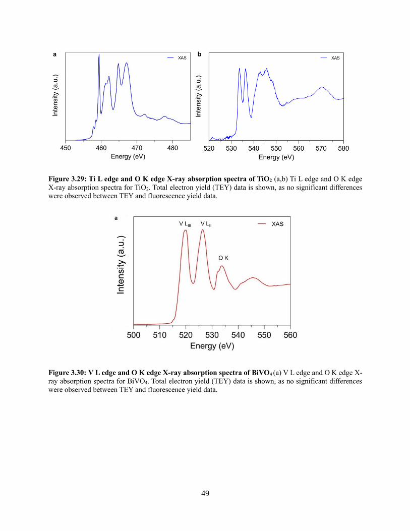
49
Figure 3.29: Ti L edge and O K edge X-ray absorption spectra of TiO2 (a,b) Ti L edge and O K edge
X-ray absorption spectra for TiO2. Total electron yield (TEY) data is shown, as no significant differences
were observed between TEY and fluorescence yield data.
Figure 3.30: V L edge and O K edge X-ray absorption spectra of BiVO4 (a) V L edge and O K edge X-
ray absorption spectra for BiVO4. Total electron yield (TEY) data is shown, as no significant differences
were observed between TEY and fluorescence yield data.
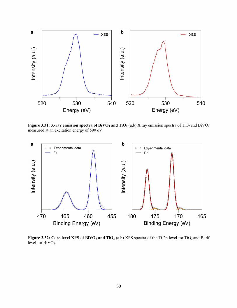
50
Figure 3.31: X-ray emission spectra of BiVO4 and TiO2 (a,b) X ray emission spectra of TiO2 and BiVO4
measured at an excitation energy of 590 eV.
Figure 3.32: Core-level XPS of BiVO4 and TiO2 (a,b) XPS spectra of the Ti 2p level for TiO2 and Bi 4f
level for BiVO4.

51
Figure 3.33: Resonant inelastic X-ray scattering of BiVO4 (b) RIXS spectra for BiVO4 on the O K edge.
Excitation energies are specified on the XAS spectrum in (a).
Figure 3.34: Resonant inelastic X-ray scattering of TiO2 (b) RIXS spectra for TiO2 on the O K edge.
Excitation energies are specified on the XAS spectrum in (a).
3.5 Conclusions
Host-guest systems are useful for achieving high performance in dual absorber
photoelectrosynthetic cells when using photoanode materials with poor intrinsic carrier transport
properties such as Fe2O3 and BiVO4. In this study we have demonstrated the use of TiO2 as a host
material for BiVO4, to provide simultaneous high light absorption and carrier collection efficiency.
We have shown how modifications of the host and guest materials can lead to higher performance,
namely by doping the TiO2 guest material, and improving the charge transfer efficiencies of the
BiVO4 by addition of a Co-based catalyst. Electrochemical and spectroscopic measurements give
evidence for the Type II band alignment necessary for favorable electron transfer from BiVO4 to

52
TiO2. We believe this architecture can be extended to improve the performance of related
photoanode materials. Achieving higher photocurrents at low potentials will allow for efficient
coupling with well-developed photocathode materials for higher bias-free solar to hydrogen
efficiencies.
3.6 References
1. Walter, M. G.; Warren, E. L.; McKone, J. R.; Boettcher, S. W.; Mi, Q.; Santori, E. A.;
Lewis, N. S. Chem. Rev. 2010, 110, (11), 6446-6473.
2. Bolton, J. R.; Strickler, S. J.; Connolly, J. S. Nature 1985, 316, (6028), 495-500.
3. Nozik, A. J. Appl. Phy. Lett. 1977, 30, (11), 567.
4. Seitz, L. C.; Chen, Z.; Forman, A. J.; Pinaud, B. A.; Benck, J. D.; Jaramillo, T. F.
ChemSusChem 2014, 7, (5), 1372-85.
5. Hu, S.; Xiang, C.; Haussener, S.; Berger, A. D.; Lewis, N. S. Energy Environ. Sci. 2013,
6, (10), 2984.
6. Liu, C.; Dasgupta, N. P.; Yang, P. Chem. Mater. 2014, 26, (1), 415-422.
7. Ni, M.; Leung, M. K. H.; Leung, D. Y. C.; Sumathy, K. Renew. Sust. Energy Rev. 2007,
11, (3), 401-425.
8. Chen, Z.; Jaramillo, T. F.; Deutsch, T. G.; Kleiman-Shwarsctein, A.; Forman, A. J.;
Gaillard, N.; Garland, R.; Takanabe, K.; Heske, C.; Sunkara, M.; McFarland, E. W.; Domen, K.;
Miller, E. L.; Turner, J. A.; Dinh, H. N. J. Mater. Res. 2011, 25, (01), 3-16.
9. Chen, Y. W.; Prange, J. D.; Duhnen, S.; Park, Y.; Gunji, M.; Chidsey, C. E.; McIntyre, P.
C. Nat. Mater. 2011, 10, (7), 539-44.
10. Hu, S.; Shaner, M. R.; Beardslee, J. A.; Lichterman, M.; Brunschwig, B. S.; Lewis, N. S.
Science 2014, 344, (6187), 1005-1009.
11. Sun, K.; Kuang, Y.; Verlage, E.; Brunschwig, B. S.; Tu, C. W.; Lewis, N. S. Adv. Energy
Mater. 2015, 5, 1402276.
12. Boettcher, S. W.; Warren, E. L.; Putnam, M. C.; Santori, E. A.; Turner-Evans, D.;
Kelzenberg, M. D.; Walter, M. G.; McKone, J. R.; Brunschwig, B. S.; Atwater, H. A.; Lewis, N.
S. J. Am. Chem. Soc. 2011, 133, (5), 1216-9.
13. Lee, M. H.; Takei, K.; Zhang, J.; Kapadia, R.; Zheng, M.; Chen, Y. Z.; Nah, J.;
Matthews, T. S.; Chueh, Y. L.; Ager, J. W.; Javey, A. Angew. Chem. Int. Ed. 2012, 51, (43),
10760-4.
14. Liu, X.; Wang, F.; Wang, Q. Phys. Chem. Chem. Phys. 2012, 14, (22), 7894-911.
15. Sivula, K.; Le Formal, F.; Gratzel, M. ChemSusChem 2011, 4, (4), 432-49.
16. Park, Y.; McDonald, K. J.; Choi, K. S. Chem. Soc. Rev. 2013, 42, (6), 2321-37.
17. Rettie, A. J. E.; Lee, H. C.; Marshall, L. G.; Lin, J.-F.; Capan, C.; Lindemuth, J.; McCloy,
J. S.; Zhou, J.; Bard, A. J.; Mullins, C. B. J. Am. Chem. Soc. 2013, 135, (30), 11389-11396.
18. Kim, T. W.; Choi, K.-S. Science 2014, 343, (6174), 990-994.
19. Robel, I.; Subramanian, V.; Kuno, M.; Kamat, P. V. J. Am. Chem. Soc. 2006, 128, (7),
2385-2393.
20. Grätzel, M. J. Photochem. Photobio. C 2003, 4, (2), 145-153.
21. Liu, H.; Tang, J.; Kramer, I. J.; Debnath, R.; Koleilat, G. I.; Wang, X.; Fisher, A.; Li, R.;
Brzozowski, L.; Levina, L.; Sargent, E. H. Adv. Mater. 2011, 23, (33), 3832-3837.
53
22. Dasgupta, N. P.; Sun, J.; Liu, C.; Brittman, S.; Andrews, S. C.; Lim, J.; Gao, H.; Yan, R.;
Yang, P. Adv. Mater. 2014, 26, (14), 2137-2184.
23. Law, M.; Greene, L. E.; Johnson, J. C.; Saykally, R.; Yang, P. Nat. Mater. 2005, 4, (6),
455-9.
24. Kim, H. S.; Lee, J. W.; Yantara, N.; Boix, P. P.; Kulkarni, S. A.; Mhaisalkar, S.; Gratzel,
M.; Park, N. G. Nano Lett. 2013, 13, (6), 2412-7.
25. Leschkies, K. S.; Divakar, R.; Basu, J.; Enache-Pommer, E.; Boercker, J. E.; Carter, C.
B.; Kortshagen, U. R.; Norris, D. J.; Aydil, E. S. Nano Lett. 2007, 7, (6), 1793-1798.
26. Lin, Y.; Zhou, S.; Sheehan, S. W.; Wang, D. J. Am. Chem. Soc. 2011, 133, (8), 2398-
2401.
27. Sivula, K.; Formal, F. L.; Grätzel, M. Chem. Mater. 2009, 21, (13), 2862-2867.
28. Stefik, M.; Cornuz, M.; Mathews, N.; Hisatomi, T.; Mhaisalkar, S.; Grätzel, M. Nano
Lett. 2012, 12, (10), 5431-5435.
29. Liu, Q.; He, J.; Yao, T.; Sun, Z.; Cheng, W.; He, S.; Xie, Y.; Peng, Y.; Cheng, H.; Sun,
Y.; Jiang, Y.; Hu, F.; Xie, Z.; Yan, W.; Pan, Z.; Wu, Z.; Wei, S. Nat. Commun. 2014, 5.
30. Pilli, S. K.; Janarthanan, R.; Deutsch, T. G.; Furtak, T. E.; Brown, L. D.; Turner, J. A.;
Herring, A. M. Phys. Chem. Chem. Phys. 2013, 15, (35), 14723-14728.
31. Rao, P. M.; Cai, L.; Liu, C.; Cho, I. S.; Lee, C. H.; Weisse, J. M.; Yang, P.; Zheng, X.
Nano Lett. 2014, 14, (2), 1099-1105.
32. Shi, X.; Choi, I. Y.; Zhang, K.; Kwon, J.; Kim, D. Y.; Lee, J. K.; Oh, S. H.; Kim, J. K.;
Park, J. H. Nat. Commun. 2014, 5, 4775.
33. Moniz, S. J. A.; Zhu, J.; Tang, J. Adv. Energy Mater. 2014, 4, (10), n/a-n/a.
34. Ho-Kimura, S.; Moniz, S. J. A.; Handoko, A. D.; Tang, J. J. Mater. Chem. A 2014, 2,
(11), 3948-3953.
35. Furubayashi, Y.; Hitosugi, T.; Yamamoto, Y.; Inaba, K.; Kinoda, G.; Hirose, Y.;
Shimada, T.; Hasegawa, T. Appl. Phys. Lett. 2005, 86, (25), 252101.
36. Taro, H.; Yutaka, F.; Atsuki, U.; Kinnosuke, I.; Kazuhisa, I.; Yasushi, H.; Go, K.; Yukio,
Y.; Toshihiro, S.; Tetsuya, H. Jpn. J. Appl. Phys. 2005, 44, (8L), L1063.
37. Shockley, W. Bell Syst. Tech. J. 1949, 28, (3), 435-489.
38. Resasco, J.; Dasgupta, N. P.; Rosell, J. R.; Guo, J.; Yang, P. J. Am. Chem. Soc. 2014,
136, (29), 10521-10526.
39. Liu, B.; Aydil, E. S. J. Am. Chem. Soc. 2009, 131, (11), 3985-3990.
40. Hausmann, D. M.; de Rouffignac, P.; Smith, A.; Gordon, R.; Monsma, D. Thin Solid
Films 2003, 443, (1–2), 1-4.
41. Kang, D.; Park, Y.; Hill, J. C.; Choi, K.-S. J. Phys. Chem. Lett. 2014, 5, (17), 2994-2999.
42. Grass, M. E.; Karlsson, P. G.; Aksoy, F.; Lundqvist, M.; Wannberg, B.; Mun, B. S.;
Hussain, Z.; Liu, Z. Rev. Sci. Instrum. 2010, 81, (5), 053106.
43. George, S. M. Chem. Rev. 2010, 110, (1), 111-131.
44. Parker, R. A. Phys. Rev. 1961, 124, (6), 1719-1722.
45. Gelderman, K.; Lee, L.; Donne, S. W. J. Chem. Educ. 2007, 84, (4), 685.
46. Cho, I. S.; Lee, C. H.; Feng, Y.; Logar, M.; Rao, P. M.; Cai, L.; Kim, D. R.; Sinclair, R.;
Zheng, X. Nat. Commun. 2013, 4, 1723.
47. Xu, M.; Da, P.; Wu, H.; Zhao, D.; Zheng, G. Nano Lett. 2012, 12, (3), 1503-1508.
48. McDonald, K. J.; Choi, K.-S. Chem. Mater. 2011, 23, (7), 1686-1693.
49. Zhong, D. K.; Choi, S.; Gamelin, D. R. J. Am. Chem. Soc. 2011, 133, (45), 18370-18377.
50. Kanan, M. W.; Nocera, D. G. Science 2008, 321, (5892), 1072-1075.
54
51. Abdi, F. F.; Firet, N.; van de Krol, R. ChemCatChem 2013, 5, (2), 490-496.
52. Park, H. S.; Kweon, K. E.; Ye, H.; Paek, E.; Hwang, G. S.; Bard, A. J. J. Phys. Chem. C
2011, 115, (36), 17870-17879.
53. Abdi, F. F.; Han, L.; Smets, A. H.; Zeman, M.; Dam, B.; van de Krol, R. Nat. Commun.
2013, 4, 2195.
54. Cooper, G.; Turner, J. A.; Nozik, A. J. J. Electrochem. Soc. 1982, 129, (9), 1973-1977.
55. Xu, Y.; Schoonen, M. A. A. Am. Mineral. 2000, 85, (3-4), 543-556.
56. Goscinski, O. Int. J. Quantum Chem. 1978, 13, (2), 263-263.
57. Cooper, J. K.; Gul, S.; Toma, F. M.; Chen, L.; Glans, P.-A.; Guo, J.; Ager, J. W.; Yano,
J.; Sharp, I. D. Chem. Mater. 2014, 26, (18), 5365-5373.
58. Cooper, J. K.; Gul, S.; Toma, F. M.; Chen, L.; Liu, Y.-S.; Guo, J.; Ager, J. W.; Yano, J.;
Sharp, I. D. J. Phys. Chem. C 2015, 119, (6), 2969-2974.
59. Axnanda, S.; Scheele, M.; Crumlin, E.; Mao, B.; Chang, R.; Rani, S.; Faiz, M.; Wang, S.;
Alivisatos, A. P.; Liu, Z. Nano Lett. 2013, 13, (12), 6176-6182.
60. Landmann, M.; Rauls, E.; Schmidt, W. J. Phys. Condens. Matter 2012, 24, (19), 195503.
55
Chapter 4
Standard methods for measuring and
reporting catalytic data for electrochemical
CO2 reduction
4.1 Introduction
The electrochemical reduction of carbon dioxide (CO2) offers an attractive means of
utilizing CO2 as a source of carbon for the production of transportation fuels and commodity
chemicals using intermittent renewable electricity, such as that produced by wind or solar energy.1-
3 Extensive efforts have been devoted to identifying electrocatalysts that can selectively and
efficiently reduce CO2 to desired products.4-7 However, objective evaluation of the activity and
selectivity of both standard and novel electrocatalysts is currently hindered by the lack of
standardized methods for preparing catalysts and electrolytes and for measuring and reporting
electrocatalytic activity. These issues are significant because the performance of electrocatalyts is
influenced not only by the composition and morphology of the electrocatalyst itself, but also by
the mass transfer of reactants to and products from the cathode of the electrochemical cell, and by
the purity of the electrocatalyst and electrolyte.
In this chapter we briefly summarize the variables that influence the measured activity
and selectivity of electrocatalysts used for CO2 reduction with the aim of establishing what
should be done to obtain reproducible data that can be attributed to properties of the catalyst
itself, and compared with data obtained by other groups. We then mention how we address these
issues to ensure that we can obtain meaningful electrocatalytic data.
4.2 Considerations when measuring electrocatalytic activity
56
4.2.1 Impact of impurities on electrocatalytic activity
To determine the intrinsic properties of a catalyst, its steady-state activity and selectivity
must be determined in the absence of significant surface contamination. If surface contamination
occurs, it is important to distinguish whether it is the result of catalytic intermediates that poison
the surface or whether it is the result of avoidable impurities introduced onto the catalyst
surface.8 The high overpotentials typically utilized to evaluate the activity of CO2 reduction
electrocatalysts are sufficient to reduce nearly any transition metal cations that might be present
in the catholyte.9, 10 In general, transition metal impurities deposited onto the electrocatalyst
surface will increase the activity of the electrocatalyst for the H2 evolution reaction (HER), since
the late transition and p-block metals typically utilized as CO2 reduction electrocatalysts have
very low activity for driving HER.11, 12 Even trace quantities (< 10 µM) of transition metal
cations can cause CO2 reduction electrocatalysts to lose their activity on the timescale of a
typical experiment.11, 12 For this reason, in the experiments throughout the remained of this
thesis, all experiments used the purest available water, electrolyte salts, and electrode materials
to avoid contaminating the surface of the electrocatalyst. Additionally, unless otherwise noted,
metallic anodes were avoided in favor of carbon-based materials. Carbon counter electrodes and
all cell components were also cleaned in ultrapure nitric acid before use to remove trace metal
impurities.13, 14
4.2.2 Impact of mass transport limitations on electrocatalytic activity
The electrochemical reduction of CO2 is highly susceptible to concentration polarization,
wherein Faradaic processes induce concentration gradients at the electrode surface. These
concentrations gradients arise due to the weakly buffered near-neutral bicarbonate solutions
typically employed as electrolytes as well as the sluggish diffusion coefficient of CO2 through
aqueous solutions.15, 16 Even modest current densities cause the pH and CO2 concentration near
the cathode surface to vary significantly from the bulk.17, 18 The magnitude of the concentration
gradients depend largely on the hydrodynamics of the electrochemical cell, which should be mixed
vigorously to ensure good mass transport to the cathode. Electrolyte mixing in our small
electrochemical cell is accomplished by agitation of the electrolyte with a column of CO2
bubbles.19-21 Activity data measured in a regime of significant concentration polarization is not
intrinsic to the behavior of the catalyst alone and may only provide transferrable knowledge to
other researchers if identical hydrodynamic conditions are replicated. Therefore, in our data we
demonstrate whether polarization effects are significant, and use continuum modeling to estimate
the magnitude of their effects.
4.2.3 Reporting electrocatalytic activity
There are several different ways to report measured electrocatalytic activity. One such
commonly used metric is faradaic efficiency, which is defined as the charge passed to produce a
specific product divided by the total faradaic charge passed. While this is a useful tool to describe
the product distribution produced by a catalyst, it is problematic when comparing different
catalysts with drastically different activities. For example, it is tempting to conclude that the
catalyst that is more selective for producing a specific product is more active for producing that
product. However, an increase in selectivity to a product may or may not be accompanied by an
increase in the rate at which that product is produced. In these cases, faradaic efficiencies can
obscure the true cause for differences between two catalysts. The rate of production of a product,

57
which is proportional to its partial current density, is a much less ambiguous descriptor of catalytic
activity. For this reason, in the remaining chapter, we will use partial currents when analyzing
catalytic data rather than Faradaic efficiencies.
4.2.4 Summary of experimental methods for measuring electrocatalytic
activity
The electrochemical experiments in the following chapters were conducted in a gas-tight
electrochemical cell machined from polyether ether ketone (PEEK). PEEK provides good
chemical and mechanical stability to prevent introduction of unwanted impurities. A schematic
of the cell is shown in Fig 4.2. Further experimental details of this cell are described in previous
works.21 The cell is composed of a cathode and anode chamber separated by an anion exchange
membrane. The surface area of the electrocatalyst in this cell relative to the electrolyte volume is large
to allow sensitive product quantification. Electrolytes are continuously purged with CO2 in this cell
through a gas dispersion frit. The exit gas stream from the cathode chamber feeds directly to a gas
chromatograph for quantification of gaseous products, while liquid products are analyzed after
electrolysis using high performance liquid chromatography. Further experimental details related to
each specific process are included in subsequent chapters.
Figure 4.1: Schematic of electrochemical cell used for testing.
4.2.5 Reproducibility in electrocatalytic activity measurements
Consistent and repeatable reports of CO2 reduction electrocatalysis are critical to advancing
the field. By first benchmarking electrochemical systems against standard catalysts, researchers
can be more confident that novel results will be repeatable at other sites, and that measured activity
can be confidently attributed to the properties of the catalyst itself. The entire electrochemical
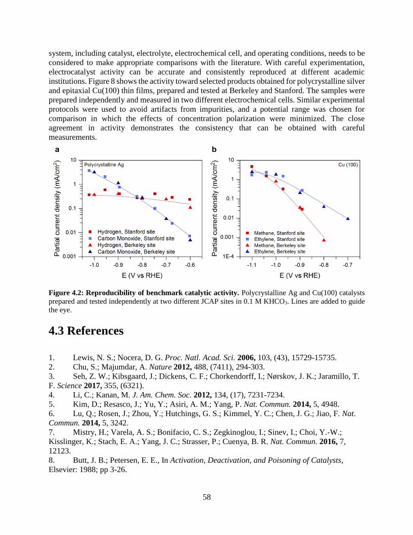
58
system, including catalyst, electrolyte, electrochemical cell, and operating conditions, needs to be
considered to make appropriate comparisons with the literature. With careful experimentation,
electrocatalyst activity can be accurate and consistently reproduced at different academic
institutions. Figure 8 shows the activity toward selected products obtained for polycrystalline silver
and epitaxial Cu(100) thin films, prepared and tested at Berkeley and Stanford. The samples were
prepared independently and measured in two different electrochemical cells. Similar experimental
protocols were used to avoid artifacts from impurities, and a potential range was chosen for
comparison in which the effects of concentration polarization were minimized. The close
agreement in activity demonstrates the consistency that can be obtained with careful
measurements.
Figure 4.2: Reproducibility of benchmark catalytic activity. Polycrystalline Ag and Cu(100) catalysts
prepared and tested independently at two different JCAP sites in 0.1 M KHCO3. Lines are added to guide
the eye.
4.3 References
1. Lewis, N. S.; Nocera, D. G. Proc. Natl. Acad. Sci. 2006, 103, (43), 15729-15735.
2. Chu, S.; Majumdar, A. Nature 2012, 488, (7411), 294-303.
3. Seh, Z. W.; Kibsgaard, J.; Dickens, C. F.; Chorkendorff, I.; Nørskov, J. K.; Jaramillo, T.
F. Science 2017, 355, (6321).
4. Li, C.; Kanan, M. J. Am. Chem. Soc. 2012, 134, (17), 7231-7234.
5. Kim, D.; Resasco, J.; Yu, Y.; Asiri, A. M.; Yang, P. Nat. Commun. 2014, 5, 4948.
6. Lu, Q.; Rosen, J.; Zhou, Y.; Hutchings, G. S.; Kimmel, Y. C.; Chen, J. G.; Jiao, F. Nat.
Commun. 2014, 5, 3242.
7. Mistry, H.; Varela, A. S.; Bonifacio, C. S.; Zegkinoglou, I.; Sinev, I.; Choi, Y.-W.;
Kisslinger, K.; Stach, E. A.; Yang, J. C.; Strasser, P.; Cuenya, B. R. Nat. Commun. 2016, 7,
12123.
8. Butt, J. B.; Petersen, E. E., In Activation, Deactivation, and Poisoning of Catalysts,
Elsevier: 1988; pp 3-26.
59
9. Hori, Y., Electrochemical CO2 Reduction on Metal Electrodes. In Modern Aspects of
Electrochemistry, Vayenas, C. G.; White, R. E.; Gamboa-Aldeco, M. E., Eds. Springer New
York: New York, NY, 2008; pp 89-189.
10. Kuhl, K. P.; Hatsukade, T.; Cave, E. R.; Abram, D. N.; Kibsgaard, J.; Jaramillo, T. F. J.
Am. Chem. Soc. 2014, 136, (40), 14107-14113.
11. Hori, Y.; Konishi, H.; Futamura, T.; Murata, A.; Koga, O.; Sakurai, H.; Oguma, K.
Electrochim. Acta 2005, 50, (27), 5354-5369.
12. Wuttig, A.; Surendranath, Y. ACS Catal. 2015, 5, (7), 4479-4484.
13. Lum, Y.; Kwon, Y.; Lobaccaro, P.; Chen, L.; Clark, E. L.; Bell, A. T.; Ager, J. W. ACS
Catal. 2016, 6, (1), 202-209.
14. Wang, L.; Ambrosi, A.; Pumera, M. Angew. Chem. Int. Ed. 2013, 52, (51), 13818-13821.
15. Butler, J. N., Carbon dioxide equilibria and their applications. CRC Press: 1991.
16. Haynes, W. M., CRC handbook of chemistry and physics. CRC press: 2014.
17. Singh, M. R.; Clark, E. L.; Bell, A. T. Phys. Chem. Chem. Phys. 2015, 17, (29), 18924-
18936.
18. Gupta, N.; Gattrell, M.; MacDougall, B. J. Appl. Electrochem. 2006, 36, (2), 161-172.
19. Clark, E. L.; Singh, M. R.; Kwon, Y.; Bell, A. T. Anal. Chem. 2015, 87, (15), 8013-8020.
20. Lobaccaro, P.; Singh, M. R.; Clark, E. L.; Kwon, Y.; Bell, A. T.; Ager, J. W. Phys.
Chem. Chem. Phys. 2016, 18, (38), 26777-26785.
21. Kuhl, K. P.; Cave, E. R.; Abram, D. N.; Jaramillo, T. F. Energy Environ. Sci. 2012, 5,
(5), 7050-7059.
60
Chapter 5
Promoter effects of alkali metal cations on
the electrochemical reduction of carbon
dioxide
This chapter contains material from the following publication:
Resasco, J.; Chen, L.D.; Clark, E.; Tsai, C.; Hahn, C.; Jaramillo, T.F.; Chan, K.; Bell, A.T J. Am.
Chem. Soc. 2017, 139, 11277-11287.
5.1 Abstract
The electrochemical reduction of CO2 is known to be influenced by the identity of the
alkali metal cation in the electrolyte; however, a satisfactory explanation for this phenomenon
has not been developed. Here we present the results of experimental and theoretical studies
aimed at elucidating the effects of electrolyte cation size on the intrinsic activity and selectivity
of metal catalysts for the reduction of CO2. Experiments were conducted under conditions where
the influence of electrolyte polarization is minimal in order to show that cation size affects the
intrinsic rates of formation of certain reaction products, most notably for HCOO-, C2H4, and
C2H5OH over Cu(100)- and Cu(111)-oriented thin films, and for CO and HCOO- over
polycrystalline Ag and Sn. Interpretation of the findings for CO2 reduction was informed by
studies of the reduction of glyoxal and CO, key intermediates along the reaction pathway to final
products. Density functional theory calculations show that the alkali metal cations influence the
distribution of products formed as a consequence of electrostatic interactions between solvated
cations present at the outer Helmholtz plane and adsorbed species having large dipole moments.
The observed trends in activity with cation size are attributed to an increase in the concentration
of cations at the outer Helmholtz plane with increasing cation size.
61
5.2 Introduction
The electrochemical reduction of CO2 offers a means for storing electrical energy
produced by renewable but intermittent resources, such as wind and solar radiation.1, 2
Hydrocarbons and alcohols, rather than carbon monoxide and formic acid, are the preferred
products of CO2 reduction because of their high energy density. Despite extensive efforts aimed
at identifying electrocatalysts that can produce these products, copper (Cu) remains the only
material capable of doing so with significant yields.3-5 Nevertheless, Cu requires a high
overpotential (~−1 V versus RHE) and produces a broad spectrum of products.6,7 Clearly, the
discovery of novel means for reducing CO2 to desirable products with higher efficiency and
selectivity is needed. To do so requires understanding the fundamental processes occurring at
the electrode surface. In addition to metal-adsorbate interactions, a full description of
electrochemical reactions must include the effects of solvation and interfacial electric fields. A
number of studies have shown that one way of influencing the product distribution is through
changes in the electrolyte cation.8-13
The role of cations is particularly interesting because a number of studies have shown
that both the activity and selectivity of Ag, Hg, and Cu for the CO2 reduction reaction (CO2RR)
are influenced significantly by the size of the alkali metal cation in the electrolyte.8-13 Similar
effects have also been observed for the electrochemical reduction of oxygen, the oxidation of
hydrogen, and the oxidation of low molecular weight alcohols.14-18 For Ag and Hg, which are
selective for CO2 reduction to carbon monoxide (CO) and formate anions (HCOO-), respectively,
increasing the alkali metal cation size increases the rates of formation of these products.8, 10, 11
For Cu, increasing alkali metal size leads to higher selectivities to C2 products, e.g., ethylene and
ethanol.9, 12, 13 Explanations for these phenomena have been attributed to differences in local pH,
or differences in kinetic overpotentials due to the electrochemical potential in the outer
Helmholtz plane being affected by cation size.8, 10, 11, 13
One of the challenges to finding a consistent interpretation for the effects of cation size
on the intrinsic kinetics of CO2 reduction is that many studies are carried out under conditions
where mass transport also contributes to the observed activity and product distribution. In recent
study, we reported the effects of cation size on the rate of the CO2RR under strong mass-
transport limitations.13 We showed that the increase in pH and the decrease in CO2 concentration
near the cathode, caused by inadequate mass transfer through the hydrodynamic boundary layer
in front of the cathode, could be offset by the hydrolysis of solvated cations. We showed that the
increased buffering effect of solvated cations with cation size could be captured theoretically and
suggested that this effect is responsible for the observed changes in the overall current density
and the distribution of product current densities with cation size. In this work, we present a
combined experimental and theoretical study of the effects of electrolyte cation size on the
intrinsic activity and selectivity of metal catalysts for the reduction of CO2. In contrast to earlier
studies, experiments were conducted at sufficiently low applied voltages to avoid the effects of
concentration polarization of the electrolyte, so that the influence of cation size on the intrinsic
activity and selectivity of each catalyst could be observed. Most of our work was conducted
using epitaxially grown Cu(100) or Cu(111) thin films; a more limited study was carried out
using polycrystalline Ag and Sn films. Density functional theory (DFT) calculations were used to
investigate how cations and cation size affect the stabilization of reaction intermediates involved
in the reduction of CO2. These calculations demonstrate that adsorbed species with large dipole

62
moments oriented away from the solvent are stabilized by electrostatic interactions with solvated
cations, while trends in activity with cation size arise from differences in ion concentration at the
Helmholtz plane.
5.3 Experimental and computational methods
5.3.1. Electrode preparation
Single-side polished Si(100) or (110) wafers (Virginia semiconductor, 1-10 Ω cm) were
diced into ~4 cm2 sized pieces that were then used as electrode substrates. Prior to Cu deposition,
the native oxide was removed from the Si substrates by submerging them in a 10% HF solution
for 5 min. Immediately after HF etching, the Si pieces were transferred to a vacuum chamber for
sputter deposition of Cu in an AJA ATC Orion-5 sputtering system. The base pressure of the
sputtering system prior to deposition was ~2x10⁻⁷ torr. The flow rate of the sputtering gas (Ar) was
25 sccm and the sputtering pressure was adjusted to 2x10⁻³ torr by controlling the speed at which
the chamber was pumped, using a variable butterfly valve. Cu (99.999% Kurt Lesker) was
deposited at a rate of 1 Å/s, as determined by a calibrated quartz crystal monitor, at ambient
temperature. The total film thickness deposited was 100 nm. Polished, polycrystalline foils of Ag
and Sn (99.99% Alfa Aesar) were also used as electrodes without further preparation.
5.3.2 Electrode characterization
The structure of the Cu thin films was characterized by X-ray diffraction. The orientation
and epitaxial quality of the films were determined using symmetric θ-2θ scans, in plane ϕ scans,
ω scans or rocking curves, and pole figures. XRD patterns were taken with a PANanalytical X'Pert
diffractometer, which uses a Cu Kα (λ = 1.54056 Å) X-ray source. Symmetric θ-2θ scans were
collected on samples fixed onto a flat glass slide in locked-coupled mode with a goniometer
resolution of 0.001°. Measured diffraction patterns were compared to known standards taken from
the International Center for Diffraction Data (ICDD) PDF4 database (card #71-4610 for Cu).
5.3.3 Electrochemical measurements
All electrochemical experiments were conducted in a gas-tight electrochemical cell machined from
polyether ether ketone (PEEK).19 The cell was cleaned with 20 wt. % nitric acid and oxidized in
UV-generated ozone for 15 min prior to the initiation of an experiment. The working and counter
electrodes were parallel and separated by an anion-conducting membrane (Selemion AMV AGC
Inc.). A gas dispersion frit was incorporated into the cathode chamber to provide vigorous
electrolyte mixing. The exposed geometric surface area of each electrode was 1 cm2 and the
electrolyte volume of each electrode chamber was 1.8 mL. The counter electrode was a Pt foil
(99.9% Sigma Aldrich) that was flame annealed prior to each experiment. The working electrode
potential was referenced against an Ag/AgCl electrode (Innovative Instruments Inc.) that was
calibrated against a homemade standard hydrogen electrode (SHE). 0.05 M M2CO3 (M referring
to an alkali metal cation) solutions were prepared by mixing ultra-pure salts (Sigma Aldrich
99.995%) and 18.2 MΩ DI, and were used as the electrolyte without further purification. The
cathode chamber was sparged with CO2 (99.999% Praxair) at a rate of 5 sccm for 20 min prior to
and throughout the duration of all electrocatalytic measurements. Upon saturation with CO2 the
pH of the electrolyte was 6.8, which was maintained throughout the duration of electrolysis.
63
Electrochemical measurements were performed using a Biologic VSP-300 potentiostat. All
electrochemical data were recorded versus the reference electrode and converted to the RHE scale.
Potentiostatic electrochemical impedance spectroscopy (PEIS) was used to determine the
uncompensated resistance (Ru) of the electrochemical cell by applying voltage waveforms about
the open circuit potential with an amplitude of 20 mV and frequencies ranging from 50 Hz to 500
kHz. The potentiostat compensated for 85% of Ru in situ and the last 15% was post-corrected to
arrive at accurate potentials. The electrocatalytic activity was assessed by conducting
chronoamperometry at each fixed applied potential for 70 min.
5.3.4 Product analysis
The effluent from the electrochemical cell was passed through the sampling loop (250 μL)
of an Agilent 7890B gas chromatograph equipped with a pulsed-discharge helium ionization
detector (PDHID). He (99.9999% Praxair) was used as the carrier gas. The effluent of the
electrochemical cell was sampled every 14 min. The gaseous products were separated using a
Hayesep-Q capillary column (Agilent) connected in series with a packed ShinCarbon ST column
(Restek Co.). The column oven was maintained at 50 °C for 1 min followed by a temperature ramp
at 30 °C/min to 250 °C, which was maintained for the duration of the analysis. The signal response
of the PDHID to each gaseous product was calibrated by analyzing a series of NIST-traceable
standard gas mixtures (Air Gas).
The electrolyte from both electrode chambers was collected after electrolysis and analyzed
using a Thermo Scientific UltiMate 3000 liquid chromatograph equipped with a refractive index
detector (RID). The electrolyte aliquots were stored in a refrigerated autosampler until analyzed
in order to minimize the evaporation of volatile products. The liquid-phase products contained in
a 10 μL sample were separated using a series of two Aminex HPX 87-H columns (Bio-Rad) and a
1 mM sulfuric acid eluent (99.999% Sigma Aldrich). The column oven was maintained at 60 °C
for the duration of the analysis. The signal response of the RID to each liquid-phase product was
calibrated by analyzing standard solutions of each product at a concentration of 1, 10, and 50 mM.
5.3.5 Theoretical calculations
Plane-wave density functional theory (DFT) employing periodic boundary conditions
was used for all calculations in this study. The Quantum ESPRESSO20 code and the Atomic
Simulation Environment (ASE)21 were used, along with ultrasoft pseudopotentials and the
Bayesian error estimation exchange-correlation functional with van der Waals interactions
(BEEF-vdW).22 This functional has been optimized for both chemisorption energies and long-
range van der Waals interactions. For all calculations, a plane-wave cutoff of 500 eV and a
density cutoff of 5000 eV were used, based on convergence tests from previous studies.23 A
Monkhorst-Pack24 k-point grid of (4×4×1) was used for (3×3) cells while a (2×2×1) grid was
used for (6×6) cells. All systems were modeled using a periodic Cu(111) slab, two ice-like water
bilayers, the solvated ion and at least 12 Å of vacuum perpendicular to the surface. The field
effect on various CO2 adsorbates without ions or solvating waters was also investigated by
applying a sawtooth potential in each simulation cell, for moderate field strengths where the
vacuum energy remains above the Fermi level.25
Constrained minima hopping26 (CMH) was used for the global optimization of water
structures surrounding each solvated ion. CMH enforces molecular identity by constraining the
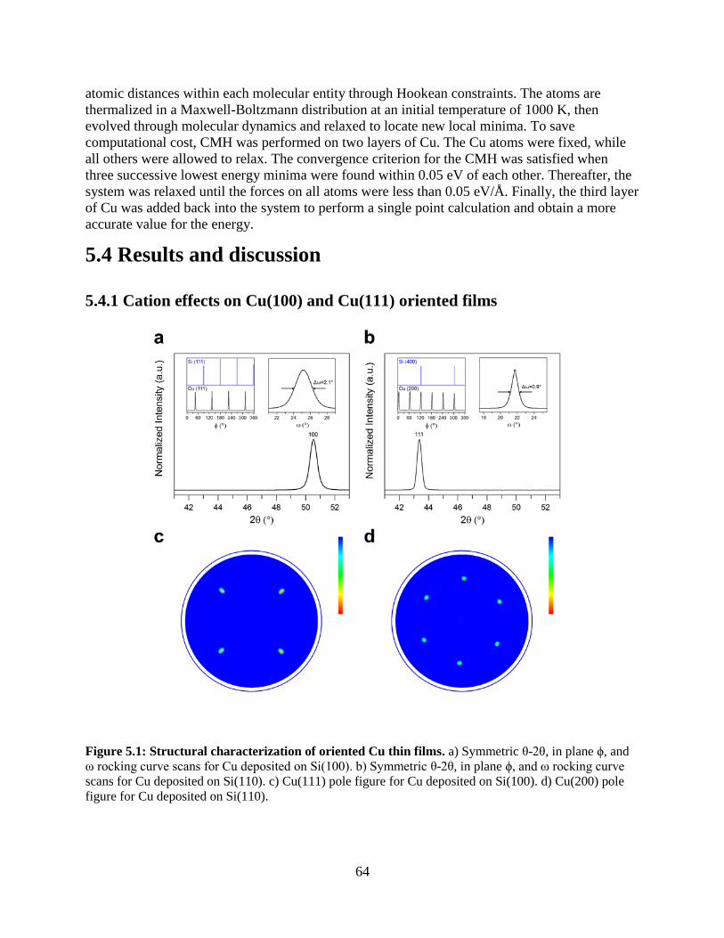
64
atomic distances within each molecular entity through Hookean constraints. The atoms are
thermalized in a Maxwell-Boltzmann distribution at an initial temperature of 1000 K, then
evolved through molecular dynamics and relaxed to locate new local minima. To save
computational cost, CMH was performed on two layers of Cu. The Cu atoms were fixed, while
all others were allowed to relax. The convergence criterion for the CMH was satisfied when
three successive lowest energy minima were found within 0.05 eV of each other. Thereafter, the
system was relaxed until the forces on all atoms were less than 0.05 eV/Å. Finally, the third layer
of Cu was added back into the system to perform a single point calculation and obtain a more
accurate value for the energy.
5.4 Results and discussion
5.4.1 Cation effects on Cu(100) and Cu(111) oriented films
Figure 5.1: Structural characterization of oriented Cu thin films. a) Symmetric θ-2θ, in plane ϕ, and
ω rocking curve scans for Cu deposited on Si(100). b) Symmetric θ-2θ, in plane ϕ, and ω rocking curve
scans for Cu deposited on Si(110). c) Cu(111) pole figure for Cu deposited on Si(100). d) Cu(200) pole
figure for Cu deposited on Si(110).

65
Epitaxially grown Cu thin films were used as electrocatalysts in order to have well-
defined catalytic surfaces.27 These films were prepared by radio-frequency sputtering of Cu onto
silicon (Si) single crystal substrates, taking advantage of the epitaxial relationship between Cu
and Si substrates of different orientations.27-28 Most of our studies were conducted on the
Cu(100) surface because it has been shown that polycrystalline Cu consists mostly of (100)
oriented crystallites and the Cu(100) surface has a higher selectivity to more desirable products
such as C2+ hydrocarbons and oxygenates (e.g., ethylene and ethanol).29-32 Symmetric θ-2θ XRD
patterns of 100 nm thick Cu films deposited on Si(100) and Si(110) substrates are shown in
Figure 1. The observation of a single Cu(200) diffraction peak for Cu deposited on Si(100)
indicates that the film is oriented with the (100) crystallographic direction normal to the film
plane. Similarly, for Cu deposited on Si(110) only the diffraction peak associated with Cu(111)
is observed.27-28 While symmetric XRD scans establish the out-of-plane texture relationships,
both out-of-plane and in-plane texture analyses are necessary to determine whether the Cu thin
films grow epitaxially on Si, as a film with strong fiber texture would show a similar diffraction
pattern. To this end, in plane-texture analysis was conducted using X-ray pole figures. Pole
figures represent the texture of a material and show the distribution of particular crystallographic
directions in a stereographic projection. The Cu(111) X-ray pole figure for Cu(100) on Si(100)
exhibits discrete Bragg reflections, indicating cube-on-cube epitaxial growth of Cu on the
Si(100) substrate. Four-fold symmetry is observed for the Cu(111) Bragg reflections with an
azimuthal angle of 90° apart, which is expected for a Cu (100) single-crystal. For Cu (111) on Si
(110), six-fold symmetry is observed for the Cu (200) Bragg reflections, indicating both strong
out-of-plane and in-plane texture and thus epitaxial growth on the Si(110) substrate (Figure 1a).
Six diffraction spots in the pole figure are seen instead of three because there are two discrete
sets of crystallites from twinning with an azimuthal angle of 60° apart. These results demonstrate
that Cu thin films can be grown epitaxially with both (100) and (111) orientations.
Figure 5.2: Effect of alkali metal cations on the total activity over Cu(100). a) Linear sweep
voltammograms for CO2 reduction on Cu(100) in CO2 saturated 0.1 M bicarbonate electrolytes containing
different metal cations. b) Average current densities obtained during bulk electrolysis as a function of
metal cation at different potentials.

66
The steady state activity and selectivity of the Cu(100) surface was investigated in CO2-
saturated bicarbonate electrolytes containing different alkali metal cations, by using
potentiometric electrolysis at potentials from −0.7 to −1.1 V vs the reversible hydrogen electrode
(RHE). Figure 2 shows the total current density as a function of electrolyte cation at various
potentials. From both steady state potentiostatic and potential sweep measurements, it is clear
that the total current density increases with cation size, and this trend is observed at all applied
potentials. To identify the contributions to the increase in the total current density, we examined
the effects of cation size on the product distribution. As large differences in total current density
exist for electrolytes containing different cations, partial currents provide a better representation
of trends in product formation rates than faradaic efficiencies.
Figure 5.3: Cation effect on the rates of formation of major products of CO2 reduction over
Cu(100). Partial current densities for each of the major products as a function of the electrolyte metal
cation on Cu(100). Data are presented at potential between −0.7 to −1.1 V vs RHE.
Figure 3 shows the partial current density for each of the major products as a function of
electrolyte cation. Formation rates of minor liquid products can be found in Table 1. A key
finding is that the production rates of hydrogen and carbon monoxide are relatively unaffected by
increasing cation size, whereas the rates of formate, ethylene, and ethanol formation increase
monotonically with increasing cation size. The rate of methane production reaches a maximum
for Na+- and K+- based electrolytes and is lower in all other electrolytes. The trends seen in Fig.
3 are consistent with previous amperometric measurements.9 It is notable that these trends are
independent of the applied overpotential.
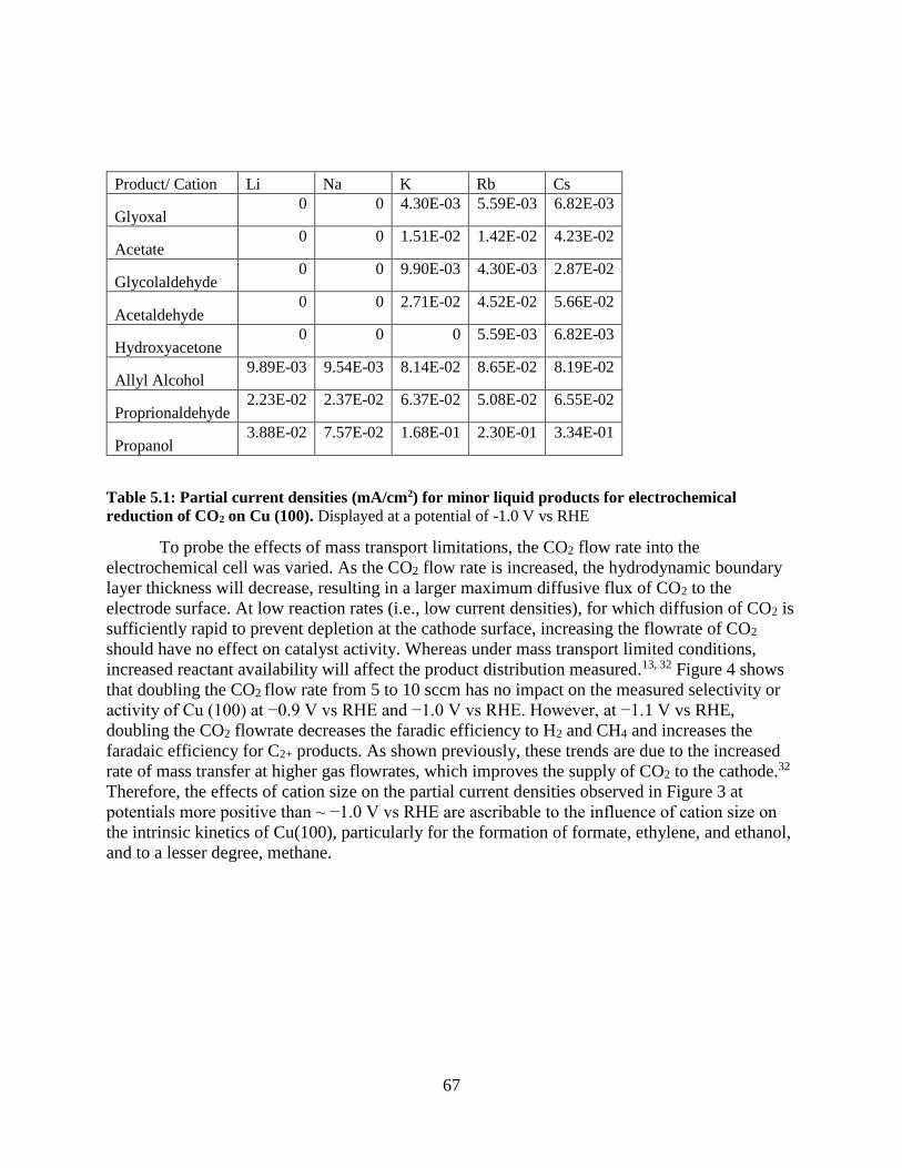
67
Product/ Cation Li Na K Rb Cs
Glyoxal 0 0 4.30E-03 5.59E-03 6.82E-03
Acetate 0 0 1.51E-02 1.42E-02 4.23E-02
Glycolaldehyde 0 0 9.90E-03 4.30E-03 2.87E-02
Acetaldehyde 0 0 2.71E-02 4.52E-02 5.66E-02
Hydroxyacetone 0 0 0 5.59E-03 6.82E-03
Allyl Alcohol 9.89E-03 9.54E-03 8.14E-02 8.65E-02 8.19E-02
Proprionaldehyde 2.23E-02 2.37E-02 6.37E-02 5.08E-02 6.55E-02
Propanol 3.88E-02 7.57E-02 1.68E-01 2.30E-01 3.34E-01
Table 5.1: Partial current densities (mA/cm2) for minor liquid products for electrochemical
reduction of CO2 on Cu (100). Displayed at a potential of -1.0 V vs RHE
To probe the effects of mass transport limitations, the CO2 flow rate into the
electrochemical cell was varied. As the CO2 flow rate is increased, the hydrodynamic boundary
layer thickness will decrease, resulting in a larger maximum diffusive flux of CO2 to the
electrode surface. At low reaction rates (i.e., low current densities), for which diffusion of CO2 is
sufficiently rapid to prevent depletion at the cathode surface, increasing the flowrate of CO2
should have no effect on catalyst activity. Whereas under mass transport limited conditions,
increased reactant availability will affect the product distribution measured.13, 32 Figure 4 shows
that doubling the CO2 flow rate from 5 to 10 sccm has no impact on the measured selectivity or
activity of Cu (100) at −0.9 V vs RHE and −1.0 V vs RHE. However, at −1.1 V vs RHE,
doubling the CO2 flowrate decreases the faradic efficiency to H2 and CH4 and increases the
faradaic efficiency for C2+ products. As shown previously, these trends are due to the increased
rate of mass transfer at higher gas flowrates, which improves the supply of CO2 to the cathode.32
Therefore, the effects of cation size on the partial current densities observed in Figure 3 at
potentials more positive than ~ −1.0 V vs RHE are ascribable to the influence of cation size on
the intrinsic kinetics of Cu(100), particularly for the formation of formate, ethylene, and ethanol,
and to a lesser degree, methane.

68
Figure 5.4: CO2 flow rate studies for probing external mass transport limitations: Current efficiency
(bars) and total current density (dots) for CO2 reduction over Cu(100) at different flow rates of CO2.
Figure 5.5: Cation effect on the rates of formation of major products of CO2 reduction over
Cu(111). Partial current densities for each of the major products as a function of the electrolyte metal
cation on Cu(111). Data are presented for the potential of -1.0 V vs RHE.
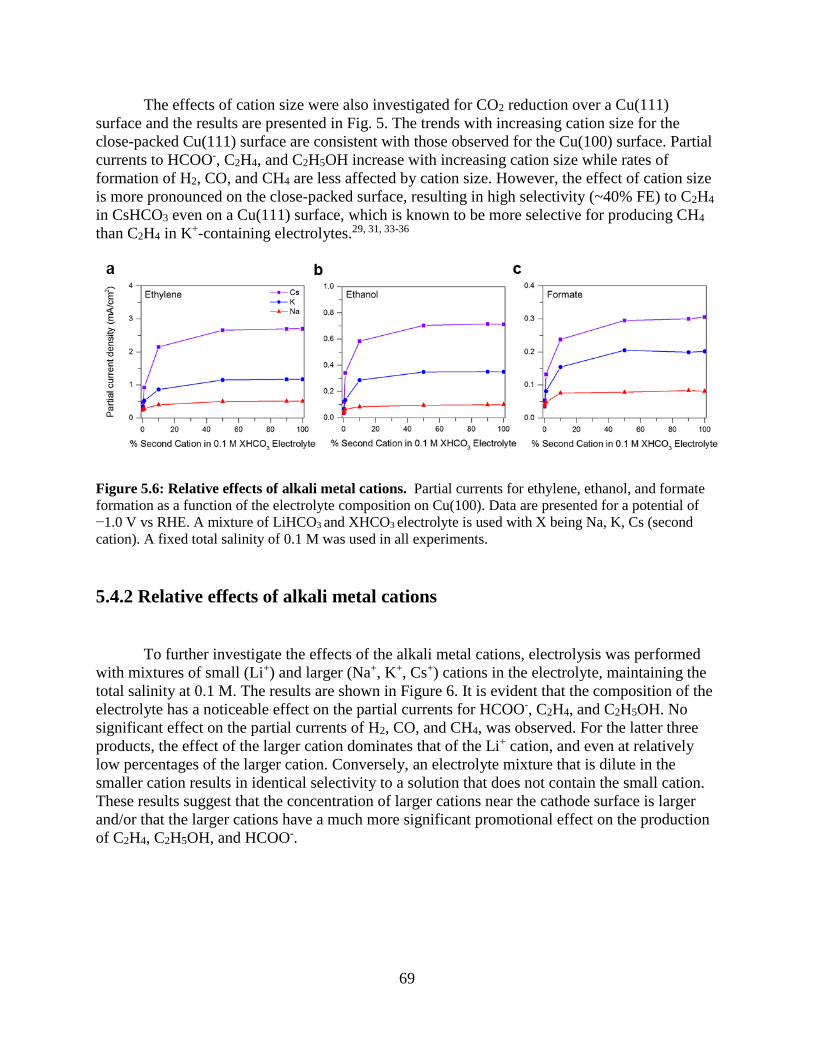
69
The effects of cation size were also investigated for CO2 reduction over a Cu(111)
surface and the results are presented in Fig. 5. The trends with increasing cation size for the
close-packed Cu(111) surface are consistent with those observed for the Cu(100) surface. Partial
currents to HCOO-, C2H4, and C2H5OH increase with increasing cation size while rates of
formation of H2, CO, and CH4 are less affected by cation size. However, the effect of cation size
is more pronounced on the close-packed surface, resulting in high selectivity (~40% FE) to C2H4
in CsHCO3 even on a Cu(111) surface, which is known to be more selective for producing CH4
than C2H4 in K+-containing electrolytes.29, 31, 33-36
Figure 5.6: Relative effects of alkali metal cations. Partial currents for ethylene, ethanol, and formate
formation as a function of the electrolyte composition on Cu(100). Data are presented for a potential of
−1.0 V vs RHE. A mixture of LiHCO3 and XHCO3 electrolyte is used with X being Na, K, Cs (second
cation). A fixed total salinity of 0.1 M was used in all experiments.
5.4.2 Relative effects of alkali metal cations
To further investigate the effects of the alkali metal cations, electrolysis was performed
with mixtures of small (Li+) and larger (Na+, K+, Cs+) cations in the electrolyte, maintaining the
total salinity at 0.1 M. The results are shown in Figure 6. It is evident that the composition of the
electrolyte has a noticeable effect on the partial currents for HCOO-, C2H4, and C2H5OH. No
significant effect on the partial currents of H2, CO, and CH4, was observed. For the latter three
products, the effect of the larger cation dominates that of the Li+ cation, and even at relatively
low percentages of the larger cation. Conversely, an electrolyte mixture that is dilute in the
smaller cation results in identical selectivity to a solution that does not contain the small cation.
These results suggest that the concentration of larger cations near the cathode surface is larger
and/or that the larger cations have a much more significant promotional effect on the production
of C2H4, C2H5OH, and HCOO-.
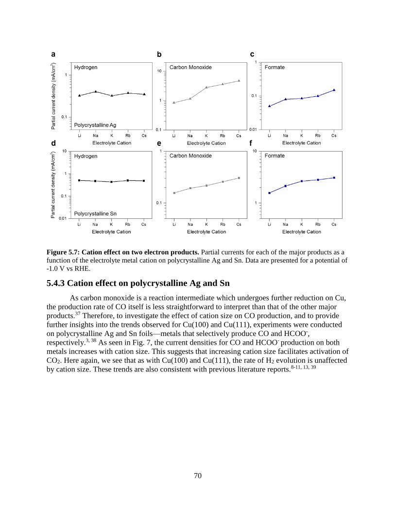
70
Figure 5.7: Cation effect on two electron products. Partial currents for each of the major products as a
function of the electrolyte metal cation on polycrystalline Ag and Sn. Data are presented for a potential of
-1.0 V vs RHE.
5.4.3 Cation effect on polycrystalline Ag and Sn
As carbon monoxide is a reaction intermediate which undergoes further reduction on Cu,
the production rate of CO itself is less straightforward to interpret than that of the other major
products.37 Therefore, to investigate the effect of cation size on CO production, and to provide
further insights into the trends observed for Cu(100) and Cu(111), experiments were conducted
on polycrystalline Ag and Sn foils—metals that selectively produce CO and HCOO-,
respectively.3, 38 As seen in Fig. 7, the current densities for CO and HCOO- production on both
metals increases with cation size. This suggests that increasing cation size facilitates activation of
CO2. Here again, we see that as with Cu(100) and Cu(111), the rate of H2 evolution is unaffected
by cation size. These trends are also consistent with previous literature reports.8-11, 13, 39
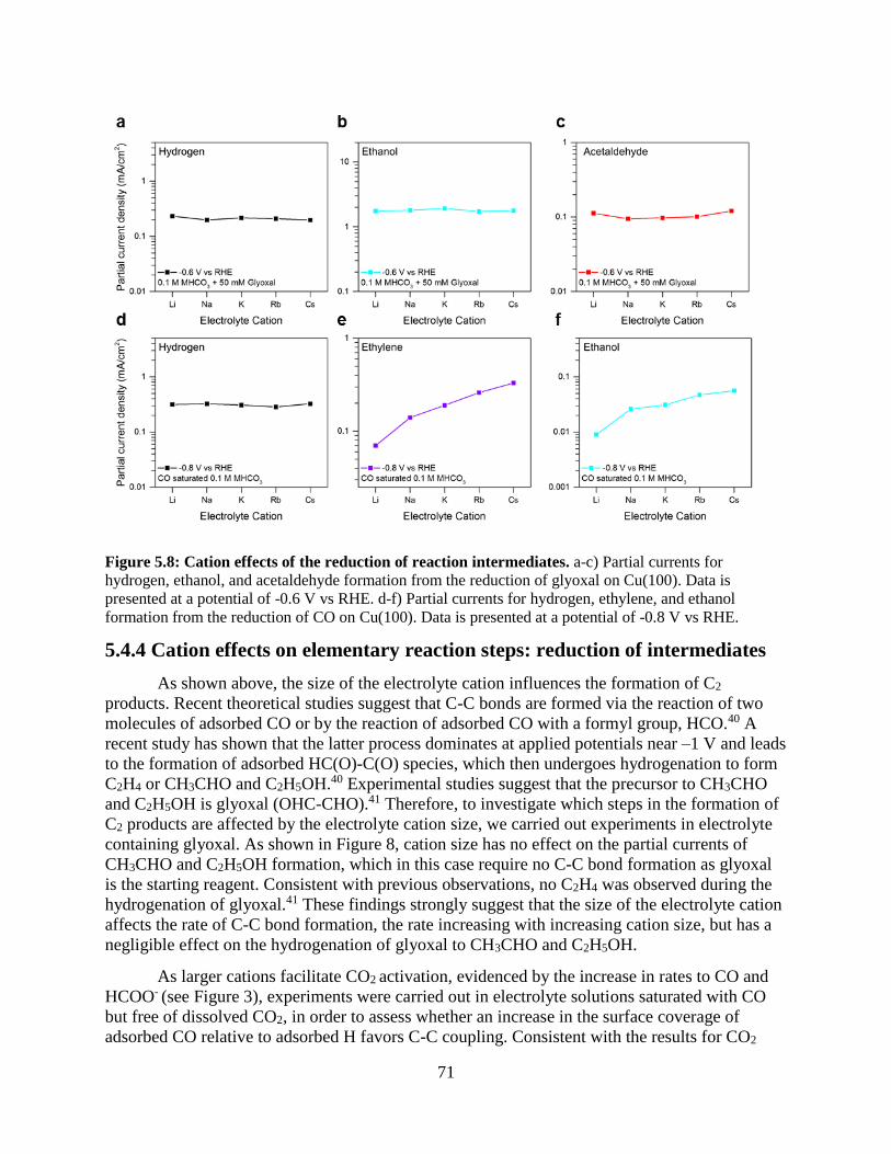
71
Figure 5.8: Cation effects of the reduction of reaction intermediates. a-c) Partial currents for
hydrogen, ethanol, and acetaldehyde formation from the reduction of glyoxal on Cu(100). Data is
presented at a potential of -0.6 V vs RHE. d-f) Partial currents for hydrogen, ethylene, and ethanol
formation from the reduction of CO on Cu(100). Data is presented at a potential of -0.8 V vs RHE.
5.4.4 Cation effects on elementary reaction steps: reduction of intermediates
As shown above, the size of the electrolyte cation influences the formation of C2
products. Recent theoretical studies suggest that C-C bonds are formed via the reaction of two
molecules of adsorbed CO or by the reaction of adsorbed CO with a formyl group, HCO.40 A
recent study has shown that the latter process dominates at applied potentials near –1 V and leads
to the formation of adsorbed HC(O)-C(O) species, which then undergoes hydrogenation to form
C2H4 or CH3CHO and C2H5OH.40 Experimental studies suggest that the precursor to CH3CHO
and C2H5OH is glyoxal (OHC-CHO).41 Therefore, to investigate which steps in the formation of
C2 products are affected by the electrolyte cation size, we carried out experiments in electrolyte
containing glyoxal. As shown in Figure 8, cation size has no effect on the partial currents of
CH3CHO and C2H5OH formation, which in this case require no C-C bond formation as glyoxal
is the starting reagent. Consistent with previous observations, no C2H4 was observed during the
hydrogenation of glyoxal.41 These findings strongly suggest that the size of the electrolyte cation
affects the rate of C-C bond formation, the rate increasing with increasing cation size, but has a
negligible effect on the hydrogenation of glyoxal to CH3CHO and C2H5OH.
As larger cations facilitate CO2 activation, evidenced by the increase in rates to CO and
HCOO- (see Figure 3), experiments were carried out in electrolyte solutions saturated with CO
but free of dissolved CO2, in order to assess whether an increase in the surface coverage of
adsorbed CO relative to adsorbed H favors C-C coupling. Consistent with the results for CO2
72
reduction over Cu(100), no change in methane activity with cation size was observed from CO
reduction at −1 V vs RHE. Figure 8b clearly shows that the rates of C2H4 and C2H5OH formation
increase with increasing cation size. We note that the magnitude of this effect is comparable to
that observed during the reduction of CO2, which shows that the effect of cation size on the
formation of multicarbon products cannot be ascribed solely to more facile CO2 activation.
5.5 Discussion
5.5.1 Cation promoter effects
The data presented in this study demonstrate that the size of the alkali metal cations in the
electrolyte affects the intrinsic rates of formation of certain reaction products. On Cu (100) and
Cu (111), these effects are most notable for HCOO-, C2H4, and C2H5OH; over polycrystalline Ag
and Sn, the effects of cation size are observed for the formation of CO and HCOO-. It is also
shown that larger cations have a stronger effect than smaller cations, and that only a small
fraction of the larger cation is needed in the electrolyte to observe its influence. Trends in the
partial current densities derived from the studies of the reduction of key reaction intermediates
(OHCCHO and CO) suggest that the elementary steps promoted by the presence of metal cations
are the activation of CO2 and the initial C-C coupling, whether through CO dimerization or CO-
CHO coupling, and not the hydrogenation of C2 intermediates leading to ethylene and ethanol.
We propose that the energetics for the formation of HCOO- and C2 products are
influenced by the presence of hydrated alkali ions located at the edge of the Helmholtz plane,
and that the observed effects of cation size are attributable to differences in the cation
concentration in the outer Helmholtz plane. This explanation is supported by DFT calculations
performed using minimum energy structures of solvated cations at the interface. Since both
Cu(100) and Cu(111) surfaces show consistent trends in activity with respect to alkali cation
size, the close-packed Cu(111) surface was chosen for the DFT simulations, which has also been
frequently used in previous theoretical CO2R studies42-45 and where the water structure is more
well-defined.46
Because the potentials applied during CO2 reduction are much more negative than the
potential of zero charge (PZC) of the low-index facets of Cu ~ −0.7VSHE 47, solvated cations
should accumulate near the surface of the electrode during reaction.40, 48 Given the very negative
reduction potentials of alkali ions, they do not chemisorb under CO2 reduction conditions. There
is also evidence from studies of oxygen reduction that the cations remain partially solvated at the
interface.49 The presence of the cation at the metal surface gives rise to high electric fields of ~
−1 V/Å in the vicinity of the ion.25, 50 In contrast to classical continuum models of the
electrochemical interface, the fields are highly localized when the structure of the cation and
solvating waters is modeled explicitly. Refs. 25, 50 show that such fields extend roughly 5 Å from
the center of the solvated cations and outside of this region decay to zero.
The strength of the adsorbate-field interaction can be probed qualitatively by the
application of a uniform field in vacuum. This approach circumvents the challenge of finding a
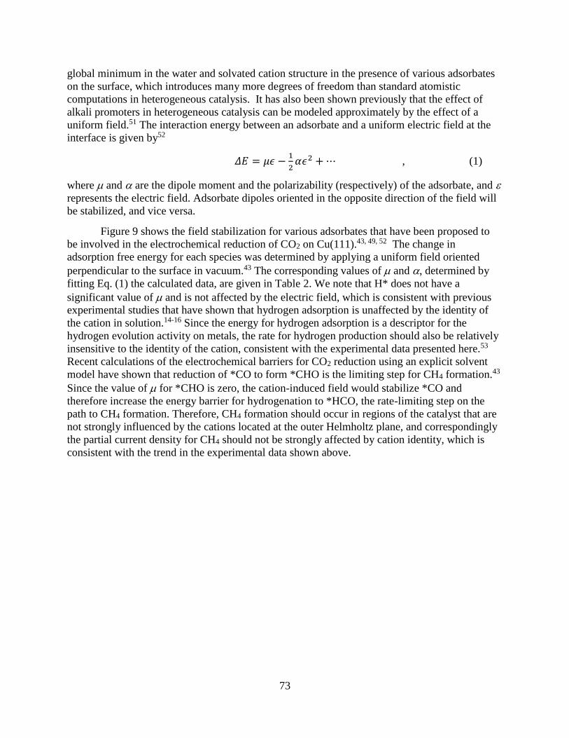
73
global minimum in the water and solvated cation structure in the presence of various adsorbates
on the surface, which introduces many more degrees of freedom than standard atomistic
computations in heterogeneous catalysis. It has also been shown previously that the effect of
alkali promoters in heterogeneous catalysis can be modeled approximately by the effect of a
uniform field.51 The interaction energy between an adsorbate and a uniform electric field at the
interface is given by52
𝛥𝐸 = 𝜇𝜖 −1
2𝛼𝜖2 + ⋯ , (1)
where and are the dipole moment and the polarizability (respectively) of the adsorbate, and represents the electric field. Adsorbate dipoles oriented in the opposite direction of the field will
be stabilized, and vice versa.
Figure 9 shows the field stabilization for various adsorbates that have been proposed to
be involved in the electrochemical reduction of CO2 on Cu(111).43, 49, 52 The change in
adsorption free energy for each species was determined by applying a uniform field oriented
perpendicular to the surface in vacuum.43 The corresponding values of and , determined by
fitting Eq. (1) the calculated data, are given in Table 2. We note that H* does not have a
significant value of and is not affected by the electric field, which is consistent with previous
experimental studies that have shown that hydrogen adsorption is unaffected by the identity of
the cation in solution.14-16 Since the energy for hydrogen adsorption is a descriptor for the
hydrogen evolution activity on metals, the rate for hydrogen production should also be relatively
insensitive to the identity of the cation, consistent with the experimental data presented here.53
Recent calculations of the electrochemical barriers for CO2 reduction using an explicit solvent
model have shown that reduction of *CO to form *CHO is the limiting step for CH4 formation.43
Since the value of for*CHO is zero, the cation-induced field would stabilize *CO and
therefore increase the energy barrier for hydrogenation to *HCO, the rate-limiting step on the
path to CH4 formation. Therefore, CH4 formation should occur in regions of the catalyst that are
not strongly influenced by the cations located at the outer Helmholtz plane, and correspondingly
the partial current density for CH4 should not be strongly affected by cation identity, which is
consistent with the trend in the experimental data shown above.

74
Figure 5.9: Field effects on various CO2R intermediates on Cu(111). The energy of each adsorbate is
plotted as a function of field strength, which is obtained by applying a uniform electric field oriented
perpendicular to the slab. The curves are fit to Equation (1) and the corresponding dipole moment and
polarizability of the adsorbates are given in Table 2. Solid curves highlight the adsorbates that are most
strongly affected by an electric field. Adsorbates with positive dipole moments oriented in the direction
opposite to the electric field) are stabilized, while adsorbates with negative (aligned with the electric
field) are destabilized.
Table 5.2 Dipole moments and polarizabilities of adsorbates on Cu(111), determined with Eq. (1)
Adsorbate (eÅ) (eÅ2/V)
*CO2 0.76 0.40
*COOH −0.19 0.60
*OCHO 0.04 0.42
*CO 0.23 0.22
*CHO 0.00 0.36
*OCCO 0.66 0.54
*OCCHO 0.75 0.74
*CHOH −0.05 0.52
*CH −0.02 0.18
*CH2 −0.08 0.26
*CH3 −0.03 0.44
*OH −0.26 0.14
*H 0.00 0.00

75
For adsorbates containing C=O bonds oriented perpendicular to the surface—in
particular, *CO2, *OCCO, and *OCCHO—the field stabilization should be large, ~ 1 eV for
fields of ~ −1 V/Å in the vicinity of the cations. As shown in Table 2, these species have the
largest dipole moments. Previous theoretical calculations have shown that on weakly binding
metals such as Ag, the field-induced stabilization of *CO2 is crucial for the activation of CO2 to
form CO.25 The barrier for the hydrogenation of *CO2 to *COOH is generally very small,54 so
stabilization of *CO2 should increase the coverage of *COOH. The *COOH species can
undergo further hydrogenation to form HCOOH or *CO. The chemical hydrogenation barriers
for *COOH to form HCOOH are surmountable at 0.69 eV and 0.75 eV on Cu(111) and Cu(211)
respectively, and 0.46eV on Ag(211),23 consistent with increased HCOOH production observed
on all of the surfaces investigated. For weakly binding metals such as Ag and Sn, the field effect
would promote CO(g) production, whereas for moderate to strongly binding metals such as Cu
and Pt, *CO produced in the vicinity of a cation would also be field stabilized, thereby
decreasing its desorption rate and increasing its *CO coverage there.
On Cu surfaces, formation of the initial intermediates to C2 products are also field-
assisted. The greater stabilization of the *OCCO relative to 2*CO in the presence of a cation is
due to the differences in the dipole moments of the product and reactant species,36 which has the
effect of lowering the barrier to C-C bond formation. In the absence of the cation-created
electrostatic field and effects of solvation by water, the barrier for this process is not
surmountable at room temperature.55 At higher overpotentials, where *CHO can be produced,
*CO-*CHO coupling would also be a feasible route towards C2 products, and the corresponding
barrier should be similarly field-stabilized due to the large dipole on *OCCHO, as shown in
Figure 9.40 Since the formation of glyoxal via addition of a hydrogen atom to *OCCHO is the
first step along the path to forming ethylene and ethanol, the observation (see Figure 8) that the
selectivity of products derived from glyoxal is independent of cation size suggests that the rate-
determining step in formation of C2 products occurs at the point of C-C bond formation and prior
to formation of glyoxal.54 The net effect of increased CO production, CO coverage and C-C
coupling on Cu on field-stabilized sites results in a net non-monotonic trend in the partial current
density for CO with cation size.
While the influence of the cation-induced field at the catalyst surface can explain the role
of cations in promoting elementary steps in the reduction of CO2 that involve strong dipole
moments, it does not explain the observed trend with cation size. We therefore explored the
possibilities that this effect is due to disparities in the magnitude of the electrostatic field induced
by cations of different size and/or an increase in the concentration of solvated cations at the outer
Helmholtz plane as a function of size.
Constrained minima hopping26 (CMH) was used to obtain the optimized structure of
water surrounding each solvated ion on Cu(111). Figure 10 shows that the calculated fields in
the vicinity of adsorbed CO (*CO) do not show a systematic variation with cation size.
Moreover, any differences in the binding energy of intermediates induced by cations would give
rise to exponential differences in current density, which we do not observe.
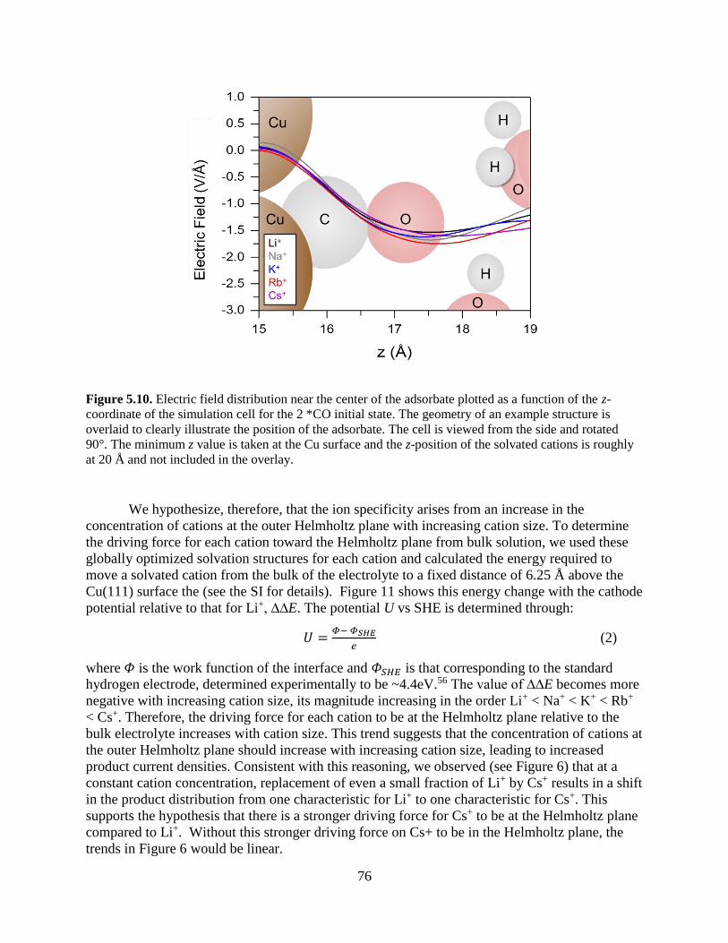
76
Figure 5.10. Electric field distribution near the center of the adsorbate plotted as a function of the z-
coordinate of the simulation cell for the 2 *CO initial state. The geometry of an example structure is
overlaid to clearly illustrate the position of the adsorbate. The cell is viewed from the side and rotated
90°. The minimum z value is taken at the Cu surface and the z-position of the solvated cations is roughly
at 20 Å and not included in the overlay.
We hypothesize, therefore, that the ion specificity arises from an increase in the
concentration of cations at the outer Helmholtz plane with increasing cation size. To determine
the driving force for each cation toward the Helmholtz plane from bulk solution, we used these
globally optimized solvation structures for each cation and calculated the energy required to
move a solvated cation from the bulk of the electrolyte to a fixed distance of 6.25 Å above the
Cu(111) surface the (see the SI for details). Figure 11 shows this energy change with the cathode
potential relative to that for Li+, ∆∆E. The potential U vs SHE is determined through:
𝑈 =𝛷− 𝛷𝑆𝐻𝐸
𝑒 (2)
where 𝛷 is the work function of the interface and 𝛷𝑆𝐻𝐸 is that corresponding to the standard
hydrogen electrode, determined experimentally to be ~4.4eV.56 The value of ∆∆E becomes more
negative with increasing cation size, its magnitude increasing in the order Li+ < Na+ < K+ < Rb+
< Cs+. Therefore, the driving force for each cation to be at the Helmholtz plane relative to the
bulk electrolyte increases with cation size. This trend suggests that the concentration of cations at
the outer Helmholtz plane should increase with increasing cation size, leading to increased
product current densities. Consistent with this reasoning, we observed (see Figure 6) that at a
constant cation concentration, replacement of even a small fraction of Li+ by Cs+ results in a shift
in the product distribution from one characteristic for Li+ to one characteristic for Cs+. This
supports the hypothesis that there is a stronger driving force for Cs+ to be at the Helmholtz plane
compared to Li+. Without this stronger driving force on Cs+ to be in the Helmholtz plane, the
trends in Figure 6 would be linear.
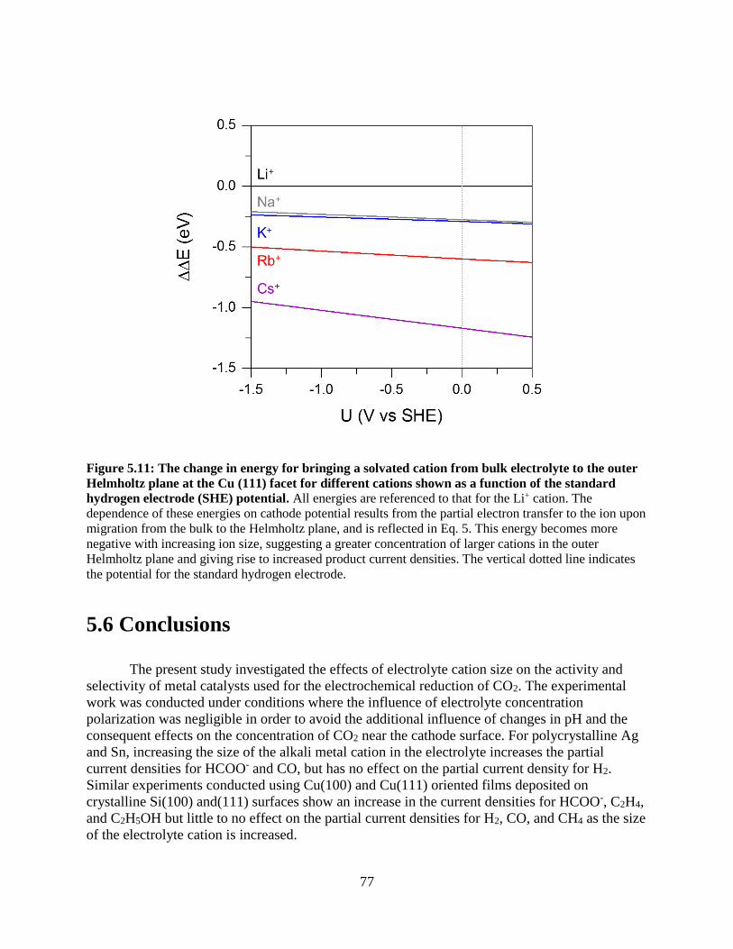
77
Figure 5.11: The change in energy for bringing a solvated cation from bulk electrolyte to the outer
Helmholtz plane at the Cu (111) facet for different cations shown as a function of the standard
hydrogen electrode (SHE) potential. All energies are referenced to that for the Li+ cation. The
dependence of these energies on cathode potential results from the partial electron transfer to the ion upon
migration from the bulk to the Helmholtz plane, and is reflected in Eq. 5. This energy becomes more
negative with increasing ion size, suggesting a greater concentration of larger cations in the outer
Helmholtz plane and giving rise to increased product current densities. The vertical dotted line indicates
the potential for the standard hydrogen electrode.
5.6 Conclusions
The present study investigated the effects of electrolyte cation size on the activity and
selectivity of metal catalysts used for the electrochemical reduction of CO2. The experimental
work was conducted under conditions where the influence of electrolyte concentration
polarization was negligible in order to avoid the additional influence of changes in pH and the
consequent effects on the concentration of CO2 near the cathode surface. For polycrystalline Ag
and Sn, increasing the size of the alkali metal cation in the electrolyte increases the partial
current densities for HCOO- and CO, but has no effect on the partial current density for H2.
Similar experiments conducted using Cu(100) and Cu(111) oriented films deposited on
crystalline Si(100) and(111) surfaces show an increase in the current densities for HCOO-, C2H4,
and C2H5OH but little to no effect on the partial current densities for H2, CO, and CH4 as the size
of the electrolyte cation is increased.
78
The observed effects are interpreted on the basis of DFT calculations. Hydrated alkali
metal cations in the outer Helmholtz plane create a dipole field of the order 1 V/Å, which can
stabilize the adsorption of surface intermediates having significant dipole moments (e.g., *CO2,
*CO, *OCCO). This field stabilization decreases the energy for the reduction of *CO2
adsorption, the precursor to two-electron products, and C-C coupling to form *OCCO or
*OCCHO, the precursor to C2H4 and C2H5OH. Calculations of the stability of the solvated cation
in the Helmholtz plane indicate that larger hydrated cations are more energetically favored at the
outer Helmholtz plane than smaller ones, which suggest a larger coverage of cations as cation
size increases. This result is consistent with the experimental observation that a small percentage
of larger cations has a large effect on product distribution.
These findings are consistent with the trends in partial current for C1 products observed
on polycrystalline Ag and Sn and on Cu(100) and Cu(111) surfaces, and for C2 products
observed on Cu(100) and Cu(111) surfaces. Also consistent with the conclusions drawn from the
theoretical analysis is that cation size affects the partial currents for C2H4 and C2H5OH produced
during the electrochemical reduction of CO over Cu(100) but has no influence on formation of
these products upon reduction of glyoxal. The absence of cation size effect on the partial current
for H2 produced on Ag, Sn, Cu(100), and Cu(111) is attributed to the absence of a dipole for *H.
Similarly, no effect of cation size on the formation of CH4 on Cu(100) and Cu(111) surfaces is
expected since the field of a cation would tend to stabilize *CO more than *CHO, thereby
increasing the energy for *CO hydrogenation to *CHO, the rate-limiting step leading to CH4.
Finally, we note that differences in the effects of electrolyte cation size on the formation
of CO on Ag and Sn vs. Cu(100) and Cu(111) are attributable to the following considerations.
For Ag and Sn, CO is a final product, and therefore only influenced by its formation by
hydrogenation of *COOH which should have an increased coverage from the field-stabilization
of *CO2. In contrast, for Cu(100) and Cu(111), *CO is an intermediate in the formation of CH4.
Since the dipole electrostatic field created by hydrated cations accelerates both the formation and
consumption of *CO, there is no observable effect of cation size on the partial current for CO on
Cu(100) and Cu(111).
5.7 References
1. Lewis, N. S.; Nocera, D. G. Proc. Natl. Acad. Sci. 2006, 103, (43), 15729-15735.
2. Chu, S.; Majumdar, A. Nature 2012, 488, (7411), 294-303.
3. Hori, Y., Electrochemical CO2 Reduction on Metal Electrodes. In Modern Aspects of
Electrochemistry, Vayenas, C. G.; White, R. E.; Gamboa-Aldeco, M. E., Eds. Springer New
York: New York, NY, 2008; pp 89-189.
4. Kuhl, K. P.; Hatsukade, T.; Cave, E. R.; Abram, D. N.; Kibsgaard, J.; Jaramillo, T. F. J.
Am. Chem. Soc. 2014, 136, (40), 14107-14113.
5. Hori, Y.; Wakebe, H.; Tsukamoto, T.; Koga, O. Electrochim. Acta 1994, 39, (11), 1833-
1839.
6. Hori, Y.; Murata, A.; Takahashi, R. J. Chem. Soc. Faraday Trans. 1 1989, 85, (8), 2309-
2326.
7. Kuhl, K. P.; Cave, E. R.; Abram, D. N.; Jaramillo, T. F. Energy Environ. Sci. 2012, 5,
(5), 7050-7059.
8. Frumkin, A. N. Trans. Faraday Soc. 1959, 55, (0), 156-167.

79
9. Akira, M.; Yoshio, H. Bull. Chem. Soc. Jpn. 1991, 64, (1), 123-127.
10. Thorson, M. R.; Siil, K. I.; Kenis, P. J. A. J. Electrochem. Soc. 2013, 160, (1), F69-F74.
11. Paik, W.; Andersen, T. N.; Eyring, H. Electrochim. Acta 1969, 14, (12), 1217-1232.
12. Kaneco, S.; Iiba, K.; Katsumata, H.; Suzuki, T.; Ohta, K. J. Solid State Electrochem.
2007, 11, (4), 490-495.
13. Singh, M. R.; Kwon, Y.; Lum, Y.; Ager, J. W.; Bell, A. T. J. Am. Chem. Soc. 2016, 138,
(39), 13006-13012.
14. Subbaraman, R.; Tripkovic, D.; Strmcnik, D.; Chang, K.-C.; Uchimura, M.; Paulikas, A.
P.; Stamenkovic, V.; Markovic, N. M. Science 2011, 334, (6060), 1256-1260.
15. Stoffelsma, C.; Rodriguez, P.; Garcia, G.; Garcia-Araez, N.; Strmcnik, D.; Marković, N.
M.; Koper, M. T. M. J. Am. Chem. Soc. 2010, 132, (45), 16127-16133.
16. Strmcnik D.; Kodama K.; van der Vliet, D.; Greeley J.; Stamenkovic, V. R.; Marković,
N. M. Nat. Chem. 2009, 1, (6), 466-472.
17. Suntivich, J.; Perry, E. E.; Gasteiger, H. A.; Shao-Horn, Y. Electrocatalysis 2013, 4, (1),
49-55.
18. Angelucci, C. A.; Varela, H.; Tremiliosi-Filho, G.; Gomes, J. F. Electrochem. Comm.
2013, 33, 10-13.
19. Lobaccaro, P.; Singh, M. R.; Clark, E. L.; Kwon, Y.; Bell, A. T.; Ager, J. W. Phys.
Chem. Chem. Phys. 2016, 18, (38), 26777-26785.
20. Giannozzi, P.; Baroni, S.; Bonini, N.; Calandra, M.; Car, R.; Cavazzoni, C.; Ceresoli, D.;
Chiarotti, G.; Cococcioni, M.; Dabo, I.; Dal Corso, A.; de Gironcoli, S.; Fabris, S.; Fratesi, G.;
Gebauer, R.; Gerstmann, U.; Gougoussis, C.; Kokalj, A.; Lazzeri, M.; Martin-Samos, L.;
Marzari, N.; Mauri, F.; Mazzarello, R.; Paolini, S.; Pasquarello, A.; Paulatto, L.; Sbraccia, C.;
Scandolo, S.; Sclauzero, G.; Seitsonen, A.; Smogunov, A.; Umari, P.; Wentzcovitch, R. J. Phys.
Condens. Matter 2009, 21, (39).
21. Bahn, S. R.; Jacobsen, K. W. Comput. Sci. Eng. 2002, 4, (3), 56--66.
22. Wellendorff, J.; Lundgaard, K. T.; Møgelhøj, A.; Petzold, V.; Landis, D. D.; Nørskov, J.
K.; Bligaard, T.; Jacobsen, K. W. Phys. Rev. B 2012, 85, (23), 235149.
23. Yoo, J. S.; Abild-Pedersen, F.; Nørskov, J. K.; Studt, F. ACS Catal. 2014, 4, (4), 1226-
1233.
24. Monkhorst, H.; Pack, J. Phys. Rev. B 1976, 13, (12), 5188-5192.
25. Chen, L. D.; Urushihara, M.; Chan, K.; Nørskov, J. ACS Catal. 2016.
26. Peterson, A. A. Top. Catal. 2013, 57, (1-4), 40-53.
27. Hahn, C.; Hatsukade, T.; Kim, Y. G.; Vailionis, A.; Baricuatro, J. H.; Higgins, D. C.;
Nitopi, S. A.; Soriaga, M. P.; Jaramillo, T. F. Proc. Natl. Acad. Sci. 2017, 114, (23), 5918-5923.
28. Jiang, H.; Klemmer, T. J.; Barnard, J. A.; Payzant, E. A. J. Vac. Sci. Technol. A 1998, 16,
(6), 3376-3383.
29. Hori, Y.; Takahashi, I.; Koga, O.; Hoshi, N. J. Phys. Chem. B 2002, 106, (1), 15-17.
30. Schouten, K. J. P.; Qin, Z.; Gallent, E. P.; Koper, M. T. M. J. Am. Chem. Soc. 2012, 134,
(24), 9864-9867.
31. Roberts, F. S.; Kuhl, K. P.; Nilsson, A. ChemCatChem 2016, 8, (6), 1119-1124.
32. Kim, Y.-G.; Baricuatro, J. H.; Javier, A.; Gregoire, J. M.; Soriaga, M. P. Langmuir 2014,
30, (50), 15053-15056.
33. Durand, W. J.; Peterson, A. A.; Studt, F.; Abild-Pedersen, F.; Nørskov, J. K. Surf. Sci.
2011, 605, (15–16), 1354-1359.
80
34. Schouten, K. J. P.; Pérez Gallent, E.; Koper, M. T. M. ACS Catal. 2013, 3, (6), 1292-
1295.
35. Montoya, J. H.; Shi, C.; Chan, K.; Nørskov, J. K. J. Phys. Chem. Lett. 2015, 6, (11),
2032-2037.
36. Sandberg, R. B.; Montoya, J. H.; Chan, K.; Nørskov, J. K. Surf. Sci. 2016, 654, 56-62.
37. Hori, Y.; Murata, A.; Yoshinami, Y. J. Chem. Soc. Faraday Trans. 1991, 87, (1), 125-
128.
38. Hatsukade, T.; Kuhl, K. P.; Cave, E. R.; Abram, D. N.; Jaramillo, T. F. Phys. Chem.
Chem. Phys. 2014, 16, (27), 13814-13819.
39. Kyriacou, G. Z.; Anagnostopoulos, A. K. J. Appl. Electrochem. 1993, 23, (5), 483-486.
40. Goodpaster, J. D.; Bell, A. T.; Head-Gordon, M. J. Phys. Chem. Lett. 2016, 7, (8), 1471-
1477.
41. Schouten, K. J. P.; Kwon, Y.; van der Ham, C. J. M.; Qin, Z.; Koper, M. T. M. Chem.
Sci. 2011, 2, (10), 1902-1909.
42. Akhade, S. A.; McCrum, I. T.; Janik, M. J. J. Electrochem. Soc. 2016, 163, (6), F477-
F484.
43. Liu, X.; Xiao, J.; Peng, H.; Hong, X.; Chan, K.; Nørskov, J. K. Nat. Commun. 2017.
44. Shi, C.; Hansen, H. A.; Lausche, A. C.; Nørskov, J. K. Phys. Chem. Chem. Phys. 2014,
16, (10), 4720-4727.
45. Xiao, H.; Cheng, T.; Goddard, W. A.; Sundararaman, R. J. Am. Chem. Soc. 2016, 138,
(2), 483-486.
46. Ogasawara, H.; Brena, B.; Nordlund, D.; Nyberg, M.; Pelmenschikov, A.; Pettersson, L.
G. M.; Nilsson, A. Phys. Rev. Lett. 2002, 89, (27), 276102.
47. Łukomska, A.; Sobkowski, J. J. Electroanal. Chem. 2004, 567, (1), 95-102.
48. Cheng, T.; Xiao, H.; Goddard, W. A. J. Am. Chem. Soc. 2016, 138, (42), 13802-13805.
49. Strmcnik, D.; van der Vliet, D. F.; Chang, K. C.; Komanicky, V.; Kodama, K.; You, H.;
Stamenkovic, V. R.; Marković, N. M. J. Phys. Chem. Lett. 2011, 2, (21), 2733-2736.
50. Montoya, J. H.; Shi, C.; Chan, K.; Norskov, J. K. J. Phys. Chem. Lett. 2015, 6, (11),
2032-2037.
51. Mortensen, J. J.; Hammer, B.; Nørskov, J. K. Phys. Rev. Lett. 1998, 80, (19), 4333-4336.
52. Nørskov, J. K. N.; Studt, F.; Abild-Pedersen, F.; Bligaard, T., Fundamental Concepts in
Heterogeneous Catalysis. Wiley, Hoboken, New Jersey: 2014.
53. Nørskov, J. K.; Bligaard, T.; Logadottir, A.; Kitchin, J. R.; Chen, J. G.; Pandelov, S.;
Stimming, U. J. Electrochem. Soc. 2005, 152, (3), J23-J26.
54. Shi, C.; O'Grady, C. P.; Peterson, A. A.; Hansen, H. A.; Nørskov, J. K. Phys. Chem.
Chem. Phys. 2013, 15, (19), 7114.
55. Montoya, J. H.; Peterson, A. A.; Nørskov, J. K. ChemCatChem 2013, 5, (3), 737-742.
56. Trasatti, S. Pure Appl. Chem. 1986, 58, (7).
81
Chapter 6
Effects of anion identity and concentration on
electrochemical reduction of CO2
6.1 Abstract
The electrochemical reduction of CO2 is known to be influenced by the concentration and
identity of the anionic species in the electrolyte; however, a full understanding of this
phenomenon has not been developed. Here we present the results of experimental and
computational studies aimed at understanding the role of electrolyte anions on the reduction of
CO2 over Cu surfaces. Experimental studies were done to show the effects of bicarbonate buffer
concentration and the composition of other buffering anions on the partial currents of the major
products formed by reduction of CO2 over Cu. It was demonstrated that the composition and
concentration of electrolyte anions has relatively little effect on the formation of CO, HCOO-,
C2H4, and CH3CH2OH, but has a significant effect on the formation of H2 and CH4. Continuum
modeling was used to assess the effects of buffering anions on the pH at the electrode surface.
The influence of pH on the activity of Cu for producing H2 and CH4 was also considered.
Changes in the pH near the electrode surface were insufficient to explain the differences in
activity and selectivity observed with changes in anion buffering capacity observed for the
formation of H2 and CH4. Therefore, it is proposed that these differences are the result of the
ability of buffering anions to donate hydrogen directly to the electrode surface and in
competition with water. The effectiveness of buffering anions to serve as hydrogen donors is
found to increase with decreasing pKa of the buffering anion.

82
6.2 Introduction
The electrochemical reduction of CO2 offers a means for storing electrical energy
produced by intermittent renewable resources, such as wind and solar radiation.1-2 Hydrocarbons
and alcohols are the preferred products of the CO2 reduction reaction (CO2RR) because of their
high energy density. To date, the only electrocatalyst that can produce these products with
significant yields is copper (Cu).3-5 While a large fraction of the total current used for the
CO2RR over Cu yields desirable products, such as ethylene (C2H4) and ethanol (CH3CH2OH), a
significant fraction of the total current goes to producing undesired products, such as hydrogen
(H2), methane (CH4), carbon monoxide (CO), and formate anions (HCOO-).6-7 Since H2 is the
largest component of the undesired products, it is desirable to identify means for enhancing the
fraction of the total current use to produce desired products of CO2 reduction by mitigating the
production of H2. To do so requires understanding of how the composition and concentration of
the electrolyte influence the mechanism of the CO2RR. We have previously demonstrated that
alkali metal cations influence the distribution of products formed as a consequence of
electrostatic interactions between solvated cations present at the outer Helmholtz plane and
adsorbed species having large dipole moments (e.g., *CO2, *CO, *OCCO).8 This field
stabilization decreases the energy for *CO2 adsorption, the precursor to two-electron products,
and C-C coupling to form *OCCO or *OCCHO, the precursor to C2H4 and C2H5OH.8 As a
consequence, the partial currents for forming H2 and CH4 are unaffected by the size of the alkali
metal cation (Li+ through Cs+), whereas the partial currents for forming HCOO-, C2H4, and
CH3CH2OH increase monotonically with increasing alkali metal cation size.
A number of studies have also shown the distribution of products formed by CO2
reduction over Cu is influenced by changes in the composition of the electrolyte anions.7-9 Hori
and coworkers have demonstrated that non-buffering anions (Cl-,ClO4-, SO4
2-) give high
selectivities to C2H4 and CH3CH2OH, and lower selectivity to CH4 and H2 compared to
bicarbonate anions (HCO3-), whereas phosphate anions (H2PO4
-) result in a higher selectivity to
H2 and CH4.7 The effects of bicarbonate concentration have also been investigated, and it was
observed that with increasing anion concentration the rates of hydrogen evolution and methane
production increased.7, 9-10 The observed differences in selectivity with buffer concentration and
buffer capacity were attributed to changes in the pH at the electrode surface; however, these
changes in pH were not quantified nor was it explained how the electrolyte pH might cause the
observed changes in product distribution.7, 9-10 Given the lack of a clear interpretation of the
effects of anion composition on the activity and selectivity of Cu for the CO2RR, we undertook
an effort to develop a complete picture of the role of anionic species on the electrochemical
reduction of CO2. Our studies show that changes in pH in the vicinity of the electrode surface are
insufficient to explain the differences in activity and selectivity observed with changes in anion
buffering capacity, and we propose that these differences are the result of the ability of buffering
anions to donate hydrogen directly to the electrode surface.
6.3 Experimental and computational methods
6.3.1. Electrode preparation
83
Cu thin films with specific crystal orientations were prepared by rf sputtering of Cu onto
silicon (Si) single crystal substrates. This approach is based on previous studies demonstrating the
epitaxial relationship between Cu and Si substrates of different orientations.8, 11, 12 The present
study utilizes Cu(100)-oriented thin films because it has been shown that this surface exhibits a
high selectivity to the desired C2+ hydrocarbons and oxygenates (e.g., C2H4 and CH3CH2OH).13
Single-side polished Si(100) wafers (Virginia semiconductor, 1-10 Ω cm) were diced into ~4 cm2
sized pieces that were then used as electrode substrates. Prior to Cu deposition, the native oxide
was removed from the Si substrates by submerging them in a 10% HF solution for 5 min.
Immediately after HF etching, the Si pieces were transferred to a vacuum chamber for sputter
deposition of Cu in an AJA ATC Orion-5 sputtering system. The base pressure of the sputtering
system prior to deposition was ~2x10⁻⁷ torr. The flow rate of the sputtering gas (Ar) was 25 sccm
and the sputtering pressure was adjusted to 2x10⁻³ torr by controlling the speed at which the
chamber was pumped, using a variable butterfly valve. Cu (99.999% Kurt Lesker) was deposited
at a rate of 1 Å/s, as determined by a calibrated quartz crystal monitor, at ambient temperature.
The total film thickness deposited was 100 nm.
6.3.2 Electrode characterization
The structure of the Cu thin films was characterized by X-ray diffraction. The orientation
and epitaxial quality of the films were determined using symmetric θ-2θ scans, in plane ϕ scans,
ω scans or rocking curves, and pole figures. XRD patterns were taken with a PANanalytical X'Pert
diffractometer, which uses a Cu Kα ( = 1.54056 Å) X-ray source. Symmetric θ-2θ scans were
collected on samples fixed onto a flat glass slide in locked-coupled mode with a goniometer
resolution of 0.001°. Measured diffraction patterns were compared to known standards taken from
the International Center for Diffraction Data (ICDD) PDF4 database (card #71-4610 for Cu). X-
ray diffraction analysis using both in plane and out of plane techniques demonstrate that Cu thin
films can be grown epitaxially with in the (100) orientation from Si(100) (Chapter 5).8
6.3.3 Electrolyte preparation
Electrolyte solutions were prepared by mixing ultra-pure salts and 18.2 MΩ DI, and were
used as the electrolyte without further purification. Bicarbonate buffered electrolytes were
prepared from K2CO3 (99.995% Sigma Aldrich) which upon saturation gave KHCO3 electrolytes
of concentrations of 0.05, 0.10, and 0.20 M. To maintain constant salinity, K2SO4 (Sigma Aldrich
99.99%) was added to these solutions to a total salinity of 0.2 M. The pH of these solutions after
CO2 saturation was 6.4, 6.8, and 7.0 respectively. Phosphate buffered electrolytes were prepared
from 0.05 M KH2PO4 (Sigma Aldrich 99.99%) and 0.05 M K2HPO4 (Sigma Aldrich 99.99%). The
pH of this solution after CO2 saturation was 6.8. Borate buffered electrolyte was prepared from
.05 M K2B4O7 (Sigma Aldrich 99.9%). The pH of this solution after CO2 saturation was 6.7.
Unbuffered solutions were prepared from 0.05 M K2SO4 and 0.1 M KClO4 (Sigma Aldrich
99.99%). The pH’s of these solutions after CO2 saturation were 4.5 and 4.0 respectively.
6.3.4 Electrochemical measurements
All electrochemical experiments were conducted in a gas-tight electrochemical cell
machined from polyether ether ketone (PEEK).14 The cell was cleaned with 20 wt. % nitric acid
84
and oxidized in UV-generated ozone for 15 min prior to the initiation of an experiment. The
working and counter electrodes were parallel and separated by an anion-conducting membrane
(Selemion AMV AGC Inc.). A gas dispersion frit was incorporated into the cathode chamber to
provide vigorous electrolyte mixing. The exposed geometric surface area of each electrode was 1
cm2 and the electrolyte volume of each electrode chamber was 1.8 mL. The counter electrode was
a Pt foil (99.9% Sigma Aldrich) that was flame annealed prior to each experiment. The working
electrode potential was referenced against an Ag/AgCl electrode (Innovative Instruments Inc.) that
was calibrated against a homemade standard hydrogen electrode (SHE). 0.05 M M2CO3 (M
referring to an alkali metal cation) solutions were prepared by mixing ultra-pure salts (Sigma
Aldrich 99.995%) and 18.2 MΩ DI, and were used as the electrolyte without further purification.
The cathode chamber was sparged with CO2 (99.999% Praxair) at a rate of 5 sccm for 20 min prior
to and throughout the duration of all electrocatalytic measurements. Upon saturation with CO2 the
pH of the electrolyte was 6.8, which was maintained throughout the duration of electrolysis.
Electrochemical measurements were performed using a Biologic VSP-300 potentiostat. All
electrochemical data were recorded versus the reference electrode and converted to the RHE scale.
Potentiostatic electrochemical impedance spectroscopy (PEIS) was used to determine the
uncompensated resistance (Ru) of the electrochemical cell by applying voltage waveforms about
the open circuit potential with an amplitude of 20 mV and frequencies ranging from 50 Hz to 500
kHz. The potentiostat compensated for 85% of Ru in situ and the last 15% was post-corrected to
arrive at accurate potentials. The electrocatalytic activity was assessed by conducting
chronoamperometry at each fixed applied potential for 70 min.
6.3.5 Product analysis
The effluent from the electrochemical cell was passed through the sampling loop (250 μL)
of an Agilent 7890B gas chromatograph equipped with a pulsed-discharge helium ionization
detector (PDHID). He (99.9999% Praxair) was used as the carrier gas. The effluent of the
electrochemical cell was sampled every 14 min. The gaseous products were separated using a
Hayesep-Q capillary column (Agilent) connected in series with a packed ShinCarbon ST column
(Restek Co.). The column oven was maintained at 50 °C for 1 min followed by a temperature ramp
at 30 °C/min to 250 °C, which was maintained for the duration of the analysis. The signal response
of the PDHID to each gaseous product was calibrated by analyzing a series of NIST-traceable
standard gas mixtures (Air Gas).
The electrolyte from both electrode chambers was collected after electrolysis and analyzed
using a Thermo Scientific UltiMate 3000 liquid chromatograph equipped with a refractive index
detector (RID). The electrolyte aliquots were stored in a refrigerated autosampler until analyzed
in order to minimize the evaporation of volatile products. The liquid-phase products contained in
a 10 μL sample were separated using a series of two Aminex HPX 87-H columns (Bio-Rad) and a
1 mM sulfuric acid eluent (99.999% Sigma Aldrich). The column oven was maintained at 60 °C
for the duration of the analysis. The signal response of the RID to each liquid-phase product was
calibrated by analyzing standard solutions of each product at a concentration of 1, 10, and 50 mM.
6.3.6 Numerical simulations
To understand the effects of transport phenomena on the measured rates of CO2
reduction, we used a diffusion-reaction model based on the work of Gupta et al. to determine the
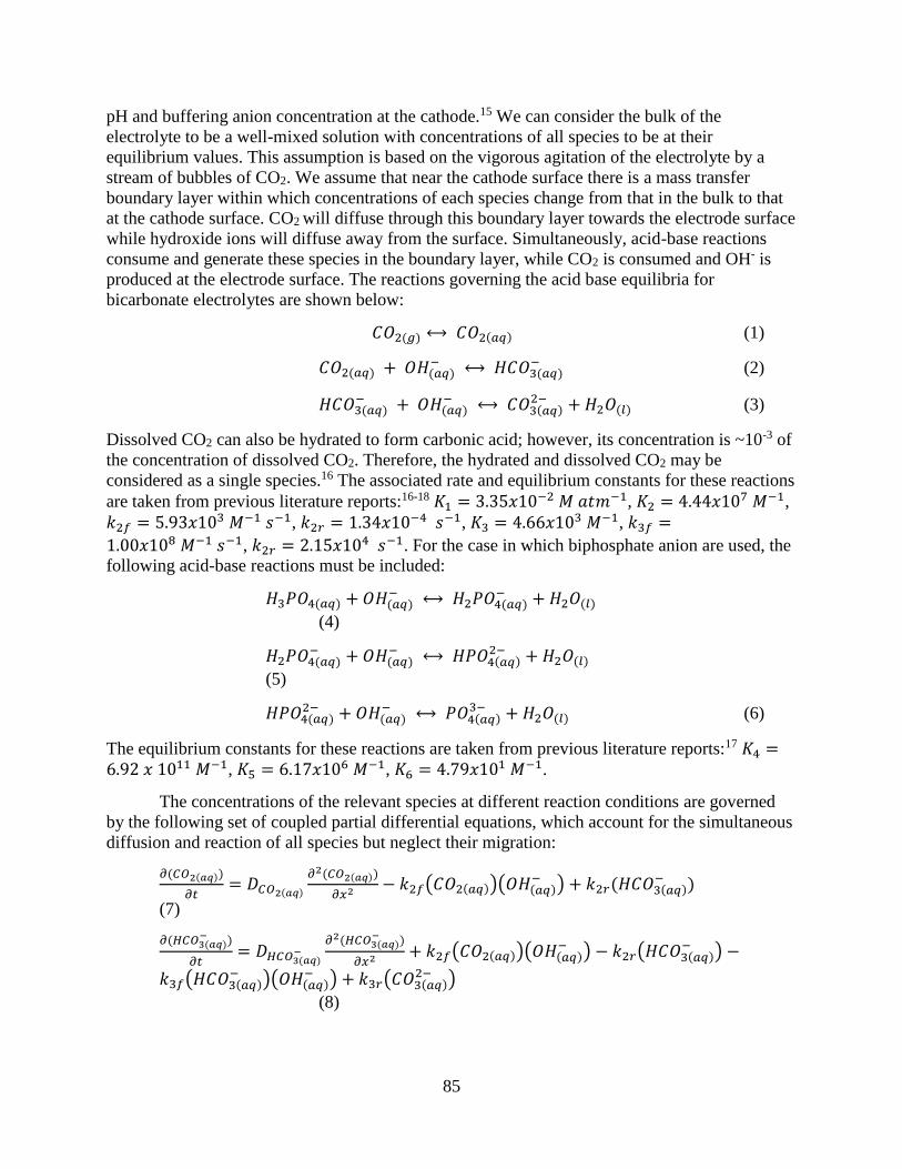
85
pH and buffering anion concentration at the cathode.15 We can consider the bulk of the
electrolyte to be a well-mixed solution with concentrations of all species to be at their
equilibrium values. This assumption is based on the vigorous agitation of the electrolyte by a
stream of bubbles of CO2. We assume that near the cathode surface there is a mass transfer
boundary layer within which concentrations of each species change from that in the bulk to that
at the cathode surface. CO2 will diffuse through this boundary layer towards the electrode surface
while hydroxide ions will diffuse away from the surface. Simultaneously, acid-base reactions
consume and generate these species in the boundary layer, while CO2 is consumed and OH- is
produced at the electrode surface. The reactions governing the acid base equilibria for
bicarbonate electrolytes are shown below:
𝐶𝑂2(𝑔) ⟷ 𝐶𝑂2(𝑎𝑞) (1)
𝐶𝑂2(𝑎𝑞) + 𝑂𝐻(𝑎𝑞)− ⟷ 𝐻𝐶𝑂3(𝑎𝑞)
− (2)
𝐻𝐶𝑂3(𝑎𝑞)− + 𝑂𝐻(𝑎𝑞)
− ⟷ 𝐶𝑂3(𝑎𝑞)2− + 𝐻2𝑂(𝑙) (3)
Dissolved CO2 can also be hydrated to form carbonic acid; however, its concentration is ~10-3 of
the concentration of dissolved CO2. Therefore, the hydrated and dissolved CO2 may be
considered as a single species.16 The associated rate and equilibrium constants for these reactions
are taken from previous literature reports:16-18 𝐾1 = 3.35𝑥10−2 𝑀 𝑎𝑡𝑚−1, 𝐾2 = 4.44𝑥107 𝑀−1,
𝑘2𝑓 = 5.93𝑥103 𝑀−1 𝑠−1, 𝑘2𝑟 = 1.34𝑥10−4 𝑠−1, 𝐾3 = 4.66𝑥103 𝑀−1, 𝑘3𝑓 =
1.00𝑥108 𝑀−1 𝑠−1, 𝑘2𝑟 = 2.15𝑥104 𝑠−1. For the case in which biphosphate anion are used, the
following acid-base reactions must be included:
𝐻3𝑃𝑂4(𝑎𝑞) + 𝑂𝐻(𝑎𝑞)− ⟷ 𝐻2𝑃𝑂4(𝑎𝑞)
− + 𝐻2𝑂(𝑙)
(4)
𝐻2𝑃𝑂4(𝑎𝑞)− + 𝑂𝐻(𝑎𝑞)
− ⟷ 𝐻𝑃𝑂4(𝑎𝑞)2− + 𝐻2𝑂(𝑙)
(5)
𝐻𝑃𝑂4(𝑎𝑞)2− + 𝑂𝐻(𝑎𝑞)
− ⟷ 𝑃𝑂4(𝑎𝑞)3− + 𝐻2𝑂(𝑙) (6)
The equilibrium constants for these reactions are taken from previous literature reports:17 𝐾4 =6.92 𝑥 1011 𝑀−1, 𝐾5 = 6.17𝑥106 𝑀−1, 𝐾6 = 4.79𝑥101 𝑀−1.
The concentrations of the relevant species at different reaction conditions are governed
by the following set of coupled partial differential equations, which account for the simultaneous
diffusion and reaction of all species but neglect their migration:
𝜕(𝐶𝑂2(𝑎𝑞))
𝜕𝑡= 𝐷𝐶𝑂2(𝑎𝑞)
𝜕2(𝐶𝑂2(𝑎𝑞))
𝜕𝑥2 − 𝑘2𝑓(𝐶𝑂2(𝑎𝑞))(𝑂𝐻(𝑎𝑞)− ) + 𝑘2𝑟(𝐻𝐶𝑂3(𝑎𝑞)
− )
(7)
𝜕(𝐻𝐶𝑂3(𝑎𝑞)− )
𝜕𝑡= 𝐷𝐻𝐶𝑂3(𝑎𝑞)
−𝜕2(𝐻𝐶𝑂3(𝑎𝑞)
− )
𝜕𝑥2+ 𝑘2𝑓(𝐶𝑂2(𝑎𝑞))(𝑂𝐻(𝑎𝑞)
− ) − 𝑘2𝑟(𝐻𝐶𝑂3(𝑎𝑞)− ) −
𝑘3𝑓(𝐻𝐶𝑂3(𝑎𝑞)− )(𝑂𝐻(𝑎𝑞)
− ) + 𝑘3𝑟(𝐶𝑂3(𝑎𝑞)2− )
(8)

86
𝜕(𝐶𝑂3(𝑎𝑞)2− )
𝜕𝑡= 𝐷𝐶𝑂3(𝑎𝑞)
2−𝜕2(𝐶𝑂3(𝑎𝑞)
2− )
𝜕𝑥2 + 𝑘3𝑓(𝐻𝐶𝑂3(𝑎𝑞)− )(𝑂𝐻(𝑎𝑞)
− ) − 𝑘3𝑟(𝐶𝑂3(𝑎𝑞)2− )
(9)
𝜕(𝑂𝐻(𝑎𝑞)− )
𝜕𝑡= 𝐷𝑂𝐻(𝑎𝑞)
−𝜕2(𝑂𝐻(𝑎𝑞)
− )
𝜕𝑥2 − 𝑘2𝑓(𝐶𝑂2(𝑎𝑞))(𝑂𝐻(𝑎𝑞)− ) + 𝑘2𝑟(𝐻𝐶𝑂3(𝑎𝑞)
− ) −
𝑘3𝑓(𝐻𝐶𝑂3(𝑎𝑞)− )(𝑂𝐻(𝑎𝑞)
− ) + 𝑘3𝑟(𝐶𝑂3(𝑎𝑞)2− )
(10)
The boundary conditions for eqns. 7-10 are set at the electrode surface (𝑥 = 0) and at the edge of
the boundary layer (𝑥 = 𝛿). A boundary layer thickness of 100 μm was assumed. This value is
comparable to that measured previously under the same flow conditions in the electrochemical
cell used for the present studies.19 At the edge of the boundary layer, the concentrations of all
species are set to their bulk equilibrium values and at the electrode surface, the experimentally
measured data give the rates of CO2 consumption and OH- generation:
𝐷𝐶𝑂2(𝑎𝑞)
𝑑(𝐶𝑂2(𝑎𝑞))
𝜕𝑥= 𝑅𝐶𝑂2 (11)
𝐷𝐻𝐶𝑂3(𝑎𝑞)−
𝑑(𝐻𝐶𝑂3(𝑎𝑞)− )
𝜕𝑥= 0 (12)
𝐷𝐶𝑂3(𝑎𝑞)2−
𝑑(𝐶𝑂3(𝑎𝑞)2− )
𝜕𝑥= 0
(13)
𝐷𝑂𝐻(𝑎𝑞)−
𝑑(𝑂𝐻(𝑎𝑞)− )
𝜕𝑥= 𝑅𝑂𝐻− (14)
Where 𝑅𝐶𝑂2 and 𝑅𝑂𝐻− are the rates of CO2 consumption and hydroxide generation respectively,
in units of moles/s cm2. Diffusion coefficients were taken from previous data:17 𝐷𝐶𝑂2(𝑎𝑞)=
1.91𝑥10−9 𝑚2𝑠−1, 𝐷𝐻𝐶𝑂3(𝑎𝑞)− = 9.23𝑥10−10 𝑚2𝑠−1, 𝐷𝐶𝑂3(𝑎𝑞)
2− = 1.19𝑥10−9 𝑚2𝑠−1, 𝐷𝑂𝐻(𝑎𝑞)− =
5.27𝑥10−9 𝑚2𝑠−1. Eqns. 7-10 together with the boundary conditions given by eqns. 11-4 were
solved using COMSOL Multiphysics 5.1 to yield pH and CO2 concentration profiles in the
hydrodynamic boundary layer.
6.4 Results and discussion
6.4.1 Buffer concentration effects on the activity of Cu(100) oriented films
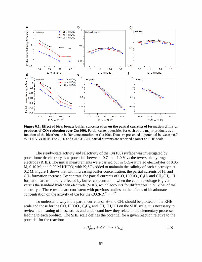
87
Figure 6.1: Effect of bicarbonate buffer concentration on the partial currents of formation of major
products of CO2 reduction over Cu(100). Partial current densities for each of the major products as a
function of the bicarbonate buffer concentration on Cu(100). Data are presented at potential between −0.7
to −1.0 V vs RHE. For C2H4 and CH3CH2OH, partial currents are reported against an SHE scale.
The steady-state activity and selectivity of the Cu(100) surface was investigated by
potentiometric electrolysis at potentials between -0.7 and -1.0 V vs the reversible hydrogen
electrode (RHE). The initial measurements were carried out in CO2-saturated electrolytes of 0.05
M, 0.10 M, and 0.20 M KHCO3 with K2SO4 added to maintain the salinity of each electrolyte at
0.2 M. Figure 1 shows that with increasing buffer concentration, the partial currents of H2 and
CH4 formation increase. By contrast, the partial currents of CO, HCOO-, C2H4 and CH3CH2OH
formation are minimally affected by buffer concentration, when the cathode voltage is given
versus the standard hydrogen electrode (SHE), which accounts for differences in bulk pH of the
electrolyte. These results are consistent with previous studies on the effects of bicarbonate
concentration on the activity of Cu for the CO2RR.7, 9, 10, 20
To understand why it the partial currents of H2 and CH4 should be plotted on the RHE
scale and those for the CO, HCOO-, C2H4, and CH3CH2OH on the SHE scale, it is necessary to
review the meaning of these scales and understand how they relate to the elementary processes
leading to each product. The SHE scale defines the potential for a given reaction relative to the
potential for the reaction:
2 𝐻(𝑎𝑞)+ + 2 𝑒− ⟷ 𝐻2(𝑔) (15)
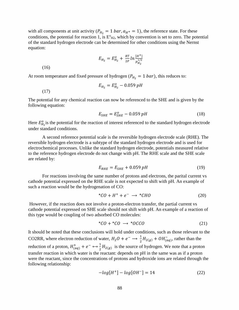
88
with all components at unit activity (𝑃𝐻2= 1 𝑏𝑎𝑟, 𝑎𝐻+ = 1), the reference state. For these
conditions, the potential for reaction 1, is EoH2, which by convention is set to zero. The potential
of the standard hydrogen electrode can be determined for other conditions using the Nernst
equation:
𝐸𝐻2= 𝐸𝐻2
𝑜 + 𝑅𝑇
2𝐹𝑙𝑛
[𝐻+]
𝑝𝐻2
1/2
(16)
At room temperature and fixed pressure of hydrogen (𝑃𝐻2= 1 𝑏𝑎𝑟), this reduces to:
𝐸𝐻2= 𝐸𝐻2
𝑜 − 0.059 𝑝𝐻
(17)
The potential for any chemical reaction can now be referenced to the SHE and is given by the
following equation:
𝐸𝑆𝐻𝐸 = 𝐸𝑆𝐻𝐸𝑜 − 0.059 𝑝𝐻 (18)
Here 𝐸𝐻2
𝑜 is the potential for the reaction of interest referenced to the standard hydrogen electrode
under standard conditions.
A second reference potential scale is the reversible hydrogen electrode scale (RHE). The
reversible hydrogen electrode is a subtype of the standard hydrogen electrode and is used for
electrochemical processes. Unlike the standard hydrogen electrode, potentials measured relative
to the reference hydrogen electrode do not change with pH. The RHE scale and the SHE scale
are related by:
𝐸𝑅𝐻𝐸 = 𝐸𝑆𝐻𝐸 + 0.059 𝑝𝐻 (19)
For reactions involving the same number of protons and electrons, the parital current vs
cathode potential expressed on the RHE scale is not expected to shift with pH. An example of
such a reaction would be the hydrogenation of CO:
*𝐶𝑂 + 𝐻+ + 𝑒− ⟶ *𝐶𝐻𝑂 (20)
However, if the reaction does not involve a proton-electron transfer, the partial current vs
cathode potential expressed on SHE scale should not shift with pH. An example of a reaction of
this type would be coupling of two adsorbed CO molecules:
*𝐶𝑂 + *𝐶𝑂 ⟶ *𝑂𝐶𝐶𝑂 (21)
It should be noted that these conclusions will hold under conditions, such as those relevant to the
CO2RR, where electron reduction of water, 𝐻2𝑂 + 𝑒− ⟶ 1
2𝐻2(𝑔) + 𝑂𝐻(𝑎𝑞)
− , rather than the
reduction of a proton, 𝐻(𝑎𝑞)+ + 𝑒− ⟷
1
2𝐻2(𝑔) is the source of hydrogen. We note that a proton
transfer reaction in which water is the reactant: depends on pH in the same was as if a proton
were the reactant, since the concentrations of protons and hydroxide ions are related through the
following relationship:
−𝑙𝑜𝑔[𝐻+] − 𝑙𝑜𝑔[𝑂𝐻−] = 14 (22)
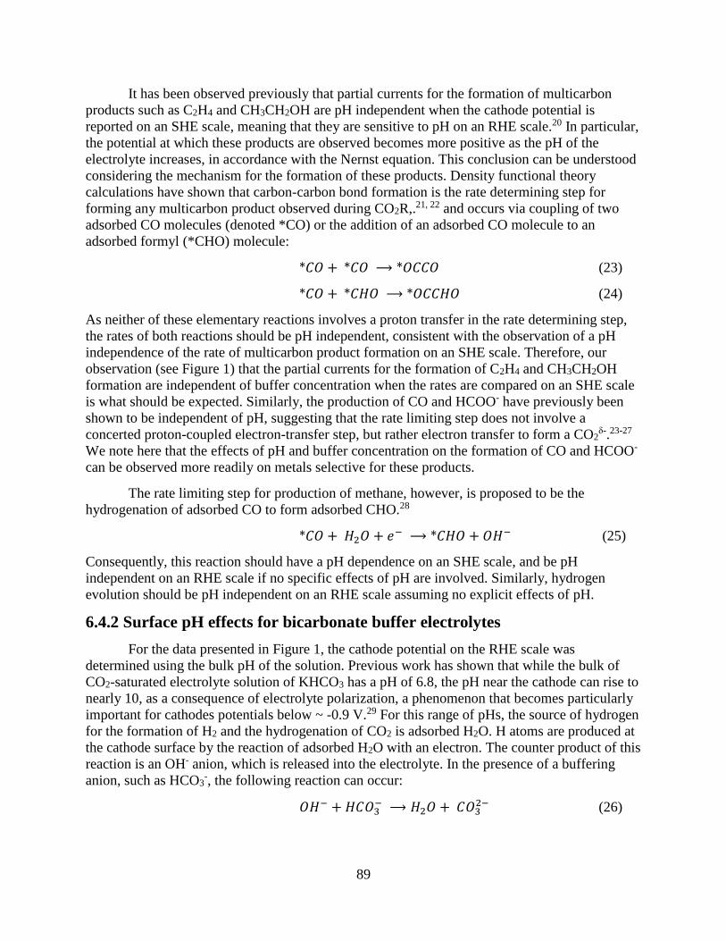
89
It has been observed previously that partial currents for the formation of multicarbon
products such as C2H4 and CH3CH2OH are pH independent when the cathode potential is
reported on an SHE scale, meaning that they are sensitive to pH on an RHE scale.20 In particular,
the potential at which these products are observed becomes more positive as the pH of the
electrolyte increases, in accordance with the Nernst equation. This conclusion can be understood
considering the mechanism for the formation of these products. Density functional theory
calculations have shown that carbon-carbon bond formation is the rate determining step for
forming any multicarbon product observed during CO2R,.21, 22 and occurs via coupling of two
adsorbed CO molecules (denoted *CO) or the addition of an adsorbed CO molecule to an
adsorbed formyl (*CHO) molecule:
*𝐶𝑂 + *𝐶𝑂 ⟶ *𝑂𝐶𝐶𝑂 (23)
*𝐶𝑂 + *𝐶𝐻𝑂 ⟶ *𝑂𝐶𝐶𝐻𝑂 (24)
As neither of these elementary reactions involves a proton transfer in the rate determining step,
the rates of both reactions should be pH independent, consistent with the observation of a pH
independence of the rate of multicarbon product formation on an SHE scale. Therefore, our
observation (see Figure 1) that the partial currents for the formation of C2H4 and CH3CH2OH
formation are independent of buffer concentration when the rates are compared on an SHE scale
is what should be expected. Similarly, the production of CO and HCOO- have previously been
shown to be independent of pH, suggesting that the rate limiting step does not involve a
concerted proton-coupled electron-transfer step, but rather electron transfer to form a CO2δ-.23-27
We note here that the effects of pH and buffer concentration on the formation of CO and HCOO-
can be observed more readily on metals selective for these products.
The rate limiting step for production of methane, however, is proposed to be the
hydrogenation of adsorbed CO to form adsorbed CHO.28
*𝐶𝑂 + 𝐻2𝑂 + 𝑒− ⟶ *𝐶𝐻𝑂 + 𝑂𝐻− (25)
Consequently, this reaction should have a pH dependence on an SHE scale, and be pH
independent on an RHE scale if no specific effects of pH are involved. Similarly, hydrogen
evolution should be pH independent on an RHE scale assuming no explicit effects of pH.
6.4.2 Surface pH effects for bicarbonate buffer electrolytes
For the data presented in Figure 1, the cathode potential on the RHE scale was
determined using the bulk pH of the solution. Previous work has shown that while the bulk of
CO2-saturated electrolyte solution of KHCO3 has a pH of 6.8, the pH near the cathode can rise to
nearly 10, as a consequence of electrolyte polarization, a phenomenon that becomes particularly
important for cathodes potentials below ~ -0.9 V.29 For this range of pHs, the source of hydrogen
for the formation of H2 and the hydrogenation of CO2 is adsorbed H2O. H atoms are produced at
the cathode surface by the reaction of adsorbed H2O with an electron. The counter product of this
reaction is an OH- anion, which is released into the electrolyte. In the presence of a buffering
anion, such as HCO3-, the following reaction can occur:
𝑂𝐻− + 𝐻𝐶𝑂3− ⟶ 𝐻2𝑂 + 𝐶𝑂3
2− (26)

90
Hydroxide anions can also react with CO2 to form bicarbonate anions, thereby depleting the
availability of the reactant. To clearly define the extent to which the pH at the cathode surface
affects partial current densities for H2 and CH4, the surface pH was calculated as a function of the
current density for different HCO3- concentrations (see Methods for full description).15, 29
Figure 6.2: Surface pH effects on the partial currents of formation of major products of CO2
reduction over Cu(100). a) pH at the electrode surface as a function of current density with increasing
bicarbonate buffer concentration. b) Partial current densities for H2 and CH4 production as a function of
the bicarbonate buffer concentration on Cu(100). Data are presented at potentials vs RHEcalc using the
calculated local pH, rather than the pH of the bulk electrolyte.
Figure 2 shows that the pH at the cathode surface is higher than that of the bulk
electrolyte, and increases with increasing current density as a consequence of the increase in the
rate of hydroxide anion formation at the cathode. However, the differences in surface pH with
buffer concentration are relatively small, particularly at low current densities, consistent with
previous calculations of the effects of buffer concentration on the local pH during CO2R.15, 29
The partial currents of H2 and CH4 production can now be examined on a calculated RHE scale.
The calculated RHE is related to the SHE potential and the pH at the electrode surface obtained
from the model, rather than the bulk electrolyte pH:
𝐸𝑅𝐻𝐸𝑐𝑎𝑙𝑐= 𝐸𝑆𝐻𝐸 + 0.059 𝑝𝐻𝑐𝑎𝑙𝑐 (25)
Figure 2 shows that substantial differences in activity persist even after differences in surface pH
with buffer concentration are taken into account. Namely, the partial currents of H2 and CH4
production increase with buffer concentration irrespective of differences in local pH.
91
Figure 6.3: The overpotential for the HER over polycrystalline Cu as a function of pH for a current
density of 2.5 mA/cm2.
Previous studies have shown that HER activity is influenced by pH, contrary to what
would be expected.30-33 To investigate the influence of this effect, HER activity measurements
were performed on a polycrystalline Cu electrode in a rotating disk electrode configuration in
order to minimize mass transfer effects. The activity was measured as a function of electrolyte
pH in the absence of CO2 in a mixture of KCl and KOH electrolytes in order to maintain the total
salinity of the electrolyte constant. Figure 3 shows that for a current density of 2.5 mA/cm2, the
overpotential for hydrogen evolution decreases with increasing electrolyte pH. This finding is
consistent with previous studies of the explicit effect of pH on the rate of hydrogen evolution,
which attribute the increase in the rate of this reaction with increasing pH to the stronger
adsorption of hydrogen atoms to the surface of Cu.34 The authors of this study explain that since
Cu binds hydrogen more weakly than would optimal for high HER activity, an increase in the
hydrogen binding energy should increase the HER activity.35 Therefore, the explicit effect of pH
on HER activity is to increase the rate of this reaction with increasing pH. One might similarly
expect the rate of methane formation to increase with increasing pH, since the rate-limiting step
for this reaction has been proposed to be *H + *CO → *HCO.28, 36 Figure 4 shows data, adapted
from Hori and coworkers, for the partial currents of methane production from CO reduction, at a
range of electrolyte pH values. Similar studies for CO2 reduction are not possible since OH- will
react with CO2 to form HCO3-. These data shows that the partial current of methane formation
increases with increasing pH, in a manner similar to that seen for hydrogen evolution. It is
notable, though, that the trends in the rates of H2 and CH4 production seen in Figures 3 and 4 are
opposite to those observed with increasing buffer concentration seen in Figure 1. In the latter
figure shows that as the highest activity is observed for the highest buffer concentration, which
has the lowest near-surface pH. What we conclude from the analysis to this point is that changes
in local pH with buffer concentration do not fully account for the observed differences in the
rates of H2 and CH4 formation.
92
Figure 6.4: pH effects on the partial currents of formation of methane during CO reduction over
polycrystalline Cu. (Adapted from Hori and coworkers)20 Partial current densities for methane at a
range of pH values. Methane activity is observed to increase with pH.
6.4.3 Buffering anions as a hydrogen source
The preceding conclusion led us to examine the hypothesis that products for which the
rate-limiting step involves hydrogen addition (H2 and CH4) should depend on the source of
hydrogen, while products for which the rate-limiting step does not involve hydrogen addition
should be unaffected by the nature of the source of hydrogen. A plausible explanation for the
trends in partial current density observed with buffer concentration is that the hydrogen for these
reaction steps may come not only from water but also from a another source, such as HCO3-.
𝐻𝐶𝑂3− + 𝑒− ⟶ *H + 𝐶𝑂3
2− (26)
While this idea has been proposed previously, little evidence for it has been given.26 We note that
even though the concentration of HCO3- is substantially lower than that of water, the pKa of
HCO3- is 4 pKa units lower than that of water, which means that HCO3
- can be considered as a
relevant hydrogen donor. For the case of HCO3-, the concentration of this anion near the cathode
surface under the conditions used in the present studies is estimated to be ~ 50% of the bulk
electrolyte concentration (0.1 M) (see SI), which is about 103 lower than the concentration of
water (55 M). On the other hand the equilibrium constant for the deprotonation of HCO3- is 104
higher than that for H2O. Therefore, it is conceivable that HCO3- could serve as a source of H
atoms.

93
Figure 6.5: Partial current densities for major products of CO2 reduction over Cu (100) in different
anionic electrolytes. Partial current densities for each of the major products as a function of the
electrolyte anion on Cu(100). All electrolytes are of a fixed potassium cation concentration of 0.1 M. Data
are presented at potential between −0.7 to −1.0 V vs RHE. For C2H4 and CH3CH2OH, partial currents are
reported against an SHE scale.
6.4.4 Buffer identity effects on the activity of Cu(100) oriented films
To investigate the possibility that buffering anions can act a source of hydrogen, the
steady state activity and selectivity of the Cu(100) surface was investigated by potentiometric
electrolysis at potentials from -0.7 to -1.0 V vs RHE carried out in CO2-saturated electrolytes
containing different anions. Potassium cations were used in all electrolytes. Two classes of
anions were used: buffering and non-buffering. For non-buffering electrolytes, the two
electrolytes chosen were perchlorate (ClO4-), which is a weakly adsorbing anion and sulfate
(SO42-), which is a more strongly adsorbing anion.37 The buffering anions were chosen to have a
range of pKa’s from 7 to 10. The buffer equilibrium reaction and the pKa for each anion are
shown below.17
𝐻𝐶𝑂3− ⟷ 𝐻+ + 𝐶𝑂3
2−, 𝑝𝐾𝑎 = 10.33 (25)
𝐵(𝑂𝐻)3 + 𝐻2𝑂 ⟷ 𝐻+ + 𝐵(𝑂𝐻)4−, 𝑝𝐾𝑎 = 9.23 (26)
𝐻2𝑃𝑂4− ⟷ 𝐻+ + 𝐻𝑃𝑂4
2−, 𝑝𝐾𝑎 = 7.21 (27)
Figure 5 shows the partial current density of each of the major products of CO2 reduction
over Cu(100) as a function of the potential for all five electrolyte compositions. The current
density for hydrogen evolution is the same for KClO4 and K2SO4, indicating that ClO4- and SO4
2-
have no effect on the rate of the HER. Because the potentials applied during CO2 reduction are

94
much more negative than the potential of zero charge (PZC) of the low-index facets of Cu, ~
−0.7 VSHE 38, solvated cations, rather than anions should accumulate near the surface of the
electrode during reaction.21, 24 On the other hand, Figure 5 shows that electrolytes containing
buffering anions yield significantly higher rate of hydrogen evolution, and that the partial current
increases in the order HCO3- < H3BO3 < HPO4
2-, in the order of decreasing pKa of the anion. The
partial current for methane production is also independent of anion identity for non-buffering
anions, but increases with decreasing pKa of the buffering anion. The partial currents of CO and
HCOO- formation are insensitive to the anion identity when compared on an SHE scale, and
have been shown previously to be independent of pH.23-26 The partial currents for C2H4 and
CH3CH2OH vs cathode potential expressed on the SHE scale is also independent of anion
identity, consistent with previous observation.20
Figure 6.6: Surface pH and anion identity effects on the partial currents of formation of major
products of CO2 reduction over Cu(100). a) pH at the electrode surface as a function of current density
with different anionic electrolytes. All electrolytes are of a fixed potassium cation concentration of 0.1 M.
b) Partial current densities for H2 and CH4 production as a function of the electrolyte identity on Cu(100).
Data are presented at potential between −0.7 to −1.1 V vs RHE using the calculated local pH, rather than
the pH of the bulk electrolyte.
6.4.5 Surface pH effects for different buffer electrolytes
To assess the extent to which differences in the partial currents for H2 and CH4 observed
for buffering and non-buffering annions are due to differences in the local pH at the cathode
surface, we calculated the local pH as a function of current density for all electrolytes. Figure 6a
show that for non-buffering anions, the surface pH is higher than that for bicarbonate anions at
any concentration. To determine whether differences in local pH could account for the
differences in the observed activity, the partial currents for H2 and CH4 production were plotted
versus the calculated RHE potential. Figures 6b and 6c shows nearly identical partial currents for
H2 and CH4 formation in electrolyte containing ClO4-, SO4
2-, or HCO3-. It is also notable that
difference between partial currents at given cathode voltage for experiments carried out in
electrolytes containing KHCO3 vs KClO4 or KSO4 is much smaller in Figure 6b than in Figure 5,
suggesting that a large part of the difference seen Figure 5 is due to the differences in the pH of
the electrolytes at the cathode surface. In unbuffered electrolyte, HCO3- ions can be formed from
reaction of CO2 with OH-, and these HCO3- ions could then act as a hydrogen source. However,
the concentration of these ions formed is estimated to be three orders of magnitude lower than
their concentration in the electrolyte with HCO3- intentionally added. The reason for the higher
than expected partial currents of HER and methane production is likely due to the more alkaline
95
pH near the electrode surface relative to the case in which buffers are added to the electrolyte.
With increasing pH, we showed above that the HER rate increases on an RHE scale, as does the
rate of methane production. Thus, HCO3- and H2O at this higher pH are competitive hydrogen
donors. Figure 6a shows that the cathode surface pH in KH2PO4 is lower than that in KHCO3;
however, Figure 6b shows that the partial current for H2 is much higher in KH2PO4 than in
KHCO3. We hypothesize that this difference is due the significantly higher ability of H2PO4- to
serve as a source of hydrogen due to its considerably lower pKa (see above). Figure 6c shows a
qualitatively similar pattern for CH4 as that seen Figure 6b for H2; however, in the case of CH4,
the partial current is much less sensitive to the anion composition, particularly at low applied
potentials, than for the formation of H2. We speculate that this difference in sensitivity could be
due to the relative importance of surface hydrogenation (via *H) versus hydrogenation from
solution (via H transfer from H2O) in the rate-limiting step for the formation of these two
products.39
6.5 Conclusions
In this study we have attempted to develop a complete picture of the role of anion
composition on the electrochemical reduction of CO2. We have confirmed that the composition
and concentration of electrolyte anions has relatively little effect on the formation of CO, HCOO-
, C2H4, and CH3CH2OH. This finding is attributed to fact that the rate-limiting step for the
formation of each of these products does not involve the addition of hydrogen atoms, a process
that can be thought of as the concerted transfer of a proton and electron or the reaction of a water
molecule and an electron with the release of a hydroxyl anion. By contrast, the formation of H2
and CH4 do exhibit a strong sensitivity to the composition and concentration of the electrolyte
anion. It is notable that once differences in the pH at the cathode surface versus the bulk
electrolyte are taken into account, significant differences in the partial currents for H2 and CH4
are still observed at a given potential vs the RHE (determined using the local pH). We propose
that these residual differences are associated with the ability of buffering anions to serve as a
significant source of hydrogen in competition with water. We note that while the concentrations
of buffering anions is much lower than that of water, the pKa’s of these anions are much larger
than that of water. The results of this study suggest that to maximize the yields of multicarbon
products such as C2H4 and CH3CH2OH, while minimizing production of H2 and CH4, one should
use electrolytes with low buffering capacity. While, these electrolytes will have a reduced ability
to mitigate changes caused by concentration polarization at high reaction rates, which will result
in a reduced faradaic efficiency to the desired products, these effects can be offset by reducing
the boundary layer thickness for mass transfer by stirring or . In view of the trade-off between
the benefits of buffering and non-buffering anions, buffering electrolytes of low salinity (0.1 M
KHCO3) are preferred to maximize the production of desired C2+ products.
6.6 References
1. Lewis, N. S.; Nocera, D. G. Proc. Natl. Acad. Sci. 2006, 103, (43), 15729-15735.
2. Chu, S.; Majumdar, A. Nature 2012, 488, (7411), 294-303.
96
3. Hori, Y.; Wakebe, H.; Tsukamoto, T.; Koga, O. Electrochim. Acta 1994, 39, (11), 1833-
1839.
4. Kuhl, K. P.; Hatsukade, T.; Cave, E. R.; Abram, D. N.; Kibsgaard, J.; Jaramillo, T. F. J.
Am. Chem. Soc. 2014, 136, (40), 14107-14113.
5. Hori, Y., Electrochemical CO2 Reduction on Metal Electrodes. In Modern Aspects of
Electrochemistry, Vayenas, C. G.; White, R. E.; Gamboa-Aldeco, M. E., Eds. Springer New
York: New York, NY, 2008; pp 89-189.
6. Kuhl, K. P.; Cave, E. R.; Abram, D. N.; Jaramillo, T. F. Energy Environ. Sci. 2012, 5,
(5), 7050-7059.
7. Hori, Y.; Murata, A.; Takahashi, R. J. Chem. Soc. Faraday Trans. 1 1989, 85, (8), 2309-
2326.
8. Resasco, J.; Chen, L. D.; Clark, E.; Tsai, C.; Hahn, C.; Jaramillo, T. F.; Chan, K.; Bell, A.
T. J. Am. Chem. Soc. 2017, 139, 11277-11287.
9. Varela, A. S.; Kroschel, M.; Reier, T.; Strasser, P. Catal. Today 2016, 260, 8-13.
10. Kas, R.; Kortlever, R.; Yılmaz, H.; Koper, M. T. M.; Mul, G. ChemElectroChem 2015, 2,
(3), 354-358.
11. Hahn, C.; Hatsukade, T.; Kim, Y.-G.; Vailionis, A.; Baricuatro, J. H.; Higgins, D. C.;
Nitopi, S. A.; Soriaga, M. P.; Jaramillo, T. F. Proc. Natl. Acad. Sci. 2017, 114, (23), 5918-5923.
12. Jiang, H.; Klemmer, T. J.; Barnard, J. A.; Payzant, E. A. J. Vac. Sci. Technol. A 1998, 16,
(6), 3376-3383.
13. Kim, Y.-G.; Baricuatro, J. H.; Javier, A.; Gregoire, J. M.; Soriaga, M. P. Langmuir 2014,
30, (50), 15053-15056.
14. Lobaccaro, P.; Singh, M. R.; Clark, E. L.; Kwon, Y.; Bell, A. T.; Ager, J. W. Phys.
Chem. Chem. Phys. 2016, 18, (38), 26777-26785.
15. Gupta, N.; Gattrell, M.; MacDougall, B. J. Appl. Electrochem. 2006, 36, (2), 161-172.
16. Butler, J. N., Carbon dioxide equilibria and their applications. CRC Press: 1991.
17. Haynes, W. M., CRC handbook of chemistry and physics. CRC press: 2014.
18. Schulz, K. G.; Riebesell, U.; Rost, B.; Thoms, S.; Zeebe, R. E. Mar. Chem. 2006, 100,
(1), 53-65.
19. Lum, Y.; Yue, B.; Lobaccaro, P.; Bell, A. T.; Ager, J. W. J. Phys. Chem. C 2017, 121,
(26), 14191-14203.
20. Hori, Y.; Takahashi, R.; Yoshinami, Y.; Murata, A. J. Phys. Chem. B 1997, 101, (36),
7075-7081.
21. Goodpaster, J. D.; Bell, A. T.; Head-Gordon, M. J. Phys. Chem. Lett. 2016, 7, (8), 1471-
1477.
22. Montoya, J. H.; Shi, C.; Chan, K.; Nørskov, J. K. J. Phys. Chem. Lett. 2015, 6, (11),
2032-2037.
23. Shi, C.; O'Grady, C. P.; Peterson, A. A.; Hansen, H. A.; Norskov, J. K. Phys. Chem.
Chem. Phys. 2013, 15, (19), 7114-7122.
24. Cheng, T.; Xiao, H.; Goddard, W. A. J. Am. Chem. Soc. 2016, 138, (42), 13802-13805.
25. Yoshio, H.; Shin, S. Bull. Chem. Soc. Jpn. 1982, 55, (3), 660-665.
26. Wuttig, A.; Yaguchi, M.; Motobayashi, K.; Osawa, M.; Surendranath, Y. Proc. Natl.
Acad. Sci. 2016, 113, (32), E4585-E4593.
27. Wuttig, A.; Yoon, Y.; Ryu, J.; Surendranath, Y. J. Am. Chem. Soc 2017, 139, 17109-
17113.
97
28. Liu, X.; Xiao, J.; Peng, H.; Hong, X.; Chan, K.; Nørskov, J. K. Nat. Commun. 2017, 8,
15438.
29. Singh, M. R.; Clark, E. L.; Bell, A. T. Phys. Chem. Chem. Phys. 2015, 17, (29), 18924-
18936.
30. Bockris, J. O. M.; Potter, E. C. J. Electrochem. Soc. 1952, 99, (4), 169-186.
31. Durst, J.; Siebel, A.; Simon, C.; Hasche, F.; Herranz, J.; Gasteiger, H. A. Energy
Environ. Sci. 2014, 7, (7), 2255-2260.
32. Strmcnik, D.; Uchimura, M.; Wang, C.; Subbaraman, R.; Danilovic, N.; van der, V.;
Paulikas, A. P.; Stamenkovic, V. R.; Markovic, N. M. Nat. Chem. 2013, 5, (4), 300-306.
33. Ledezma-Yanez, I.; Wallace, W. D. Z.; Sebastián-Pascual, P.; Climent, V.; Feliu, J. M.;
Koper, M. T. M. Nat. Energy 2017, 2, 17031.
34. Sheng, W.; Zhuang, Z.; Gao, M.; Zheng, J.; Chen, J. G.; Yan, Y. Nat. Commun. 2015, 6,
5848.
35. Nørskov, J. K.; Bligaard, T.; Logadottir, A.; Kitchin, J. R.; Chen, J. G.; Pandelov, S.;
Stimming, U. J. Electrochem. Soc. 2005, 152, (3), J23-J26.
36. Peterson, A. A.; Abild-Pedersen, F.; Studt, F.; Rossmeisl, J.; Norskov, J. K. Energy
Environ. Sci. 2010, 3, (9), 1311-1315.
37. Mostany, J.; Herrero, E.; Feliu, J. M.; Lipkowski, J. J. Phys. Chem. B 2002, 106, (49),
12787-12796.
38. Łukomska, A.; Sobkowski, J. J. Electroanal. Chem. 2004, 567, (1), 95-102.
39. Cheng, T.; Xiao, H.; Goddard, W. A. Proc. Natl. Acad. Sci. 2017, 114, (8), 1795-1800.