reprogramming the on-chip flash memory using the i2c bus
TRANSCRIPT

To our customers,
Old Company Name in Catalogs and Other Documents
On April 1st, 2010, NEC Electronics Corporation merged with Renesas Technology
Corporation, and Renesas Electronics Corporation took over all the business of both companies. Therefore, although the old company name remains in this document, it is a valid Renesas Electronics document. We appreciate your understanding.
Renesas Electronics website: http://www.renesas.com
April 1st, 2010 Renesas Electronics Corporation
Issued by: Renesas Electronics Corporation (http://www.renesas.com)
Send any inquiries to http://www.renesas.com/inquiry.

Notice 1. All information included in this document is current as of the date this document is issued. Such information, however, is
subject to change without any prior notice. Before purchasing or using any Renesas Electronics products listed herein, please confirm the latest product information with a Renesas Electronics sales office. Also, please pay regular and careful attention to additional and different information to be disclosed by Renesas Electronics such as that disclosed through our website.
2. Renesas Electronics does not assume any liability for infringement of patents, copyrights, or other intellectual property rights of third parties by or arising from the use of Renesas Electronics products or technical information described in this document. No license, express, implied or otherwise, is granted hereby under any patents, copyrights or other intellectual property rights of Renesas Electronics or others.
3. You should not alter, modify, copy, or otherwise misappropriate any Renesas Electronics product, whether in whole or in part. 4. Descriptions of circuits, software and other related information in this document are provided only to illustrate the operation of
semiconductor products and application examples. You are fully responsible for the incorporation of these circuits, software, and information in the design of your equipment. Renesas Electronics assumes no responsibility for any losses incurred by you or third parties arising from the use of these circuits, software, or information.
5. When exporting the products or technology described in this document, you should comply with the applicable export control laws and regulations and follow the procedures required by such laws and regulations. You should not use Renesas Electronics products or the technology described in this document for any purpose relating to military applications or use by the military, including but not limited to the development of weapons of mass destruction. Renesas Electronics products and technology may not be used for or incorporated into any products or systems whose manufacture, use, or sale is prohibited under any applicable domestic or foreign laws or regulations.
6. Renesas Electronics has used reasonable care in preparing the information included in this document, but Renesas Electronics does not warrant that such information is error free. Renesas Electronics assumes no liability whatsoever for any damages incurred by you resulting from errors in or omissions from the information included herein.
7. Renesas Electronics products are classified according to the following three quality grades: “Standard”, “High Quality”, and “Specific”. The recommended applications for each Renesas Electronics product depends on the product’s quality grade, as indicated below. You must check the quality grade of each Renesas Electronics product before using it in a particular application. You may not use any Renesas Electronics product for any application categorized as “Specific” without the prior written consent of Renesas Electronics. Further, you may not use any Renesas Electronics product for any application for which it is not intended without the prior written consent of Renesas Electronics. Renesas Electronics shall not be in any way liable for any damages or losses incurred by you or third parties arising from the use of any Renesas Electronics product for an application categorized as “Specific” or for which the product is not intended where you have failed to obtain the prior written consent of Renesas Electronics. The quality grade of each Renesas Electronics product is “Standard” unless otherwise expressly specified in a Renesas Electronics data sheets or data books, etc.
“Standard”: Computers; office equipment; communications equipment; test and measurement equipment; audio and visual equipment; home electronic appliances; machine tools; personal electronic equipment; and industrial robots.
“High Quality”: Transportation equipment (automobiles, trains, ships, etc.); traffic control systems; anti-disaster systems; anti-crime systems; safety equipment; and medical equipment not specifically designed for life support.
“Specific”: Aircraft; aerospace equipment; submersible repeaters; nuclear reactor control systems; medical equipment or systems for life support (e.g. artificial life support devices or systems), surgical implantations, or healthcare intervention (e.g. excision, etc.), and any other applications or purposes that pose a direct threat to human life.
8. You should use the Renesas Electronics products described in this document within the range specified by Renesas Electronics, especially with respect to the maximum rating, operating supply voltage range, movement power voltage range, heat radiation characteristics, installation and other product characteristics. Renesas Electronics shall have no liability for malfunctions or damages arising out of the use of Renesas Electronics products beyond such specified ranges.
9. Although Renesas Electronics endeavors to improve the quality and reliability of its products, semiconductor products have specific characteristics such as the occurrence of failure at a certain rate and malfunctions under certain use conditions. Further, Renesas Electronics products are not subject to radiation resistance design. Please be sure to implement safety measures to guard them against the possibility of physical injury, and injury or damage caused by fire in the event of the failure of a Renesas Electronics product, such as safety design for hardware and software including but not limited to redundancy, fire control and malfunction prevention, appropriate treatment for aging degradation or any other appropriate measures. Because the evaluation of microcomputer software alone is very difficult, please evaluate the safety of the final products or system manufactured by you.
10. Please contact a Renesas Electronics sales office for details as to environmental matters such as the environmental compatibility of each Renesas Electronics product. Please use Renesas Electronics products in compliance with all applicable laws and regulations that regulate the inclusion or use of controlled substances, including without limitation, the EU RoHS Directive. Renesas Electronics assumes no liability for damages or losses occurring as a result of your noncompliance with applicable laws and regulations.
11. This document may not be reproduced or duplicated, in any form, in whole or in part, without prior written consent of Renesas Electronics.
12. Please contact a Renesas Electronics sales office if you have any questions regarding the information contained in this document or Renesas Electronics products, or if you have any other inquiries.
(Note 1) “Renesas Electronics” as used in this document means Renesas Electronics Corporation and also includes its majority-owned subsidiaries.
(Note 2) “Renesas Electronics product(s)” means any product developed or manufactured by or for Renesas Electronics.
APPLICATION NOTE
REJ06B0217-0100Z/Rev.1.00 December 2003 Page 1 of 90
H8/300H Tiny SeriesReprogramming the On-Chip Flash Memory Using the I2C Bus
IntroductionYou can use the I2C bus interface of the H8/3664 to reprogram the contents of the on-chip flash memory.
Target DeviceH8/300H Tiny Series H8/3664 CPU
Contents
1. Specifications.................................................................................................................................... 2
2. Detailed Specifications...................................................................................................................... 3
3. Description of Software................................................................................................................... 11
4. Hierarchy of Modules ...................................................................................................................... 18
5. Flowcharts....................................................................................................................................... 19
6. Description of Software................................................................................................................... 38
7. Hierarchy of Modules ...................................................................................................................... 44
8. Flowcharts....................................................................................................................................... 45
9. Header File List ............................................................................................................................... 64
10. Program Listing............................................................................................................................... 66

H8/300H Tiny SeriesReprogramming the On-Chip Flash Memory Using the I2C Bus
REJ06B0217-0100Z/Rev.1.00 December 2003 Page 2 of 90
1. Specifications• The I2C bus of the H8/3664 is used to reprogram the contents of the on-chip flash memory. The transfer source
(H8/3664) sends the contents of a user program in its on-chip flash memory (addresses H'1000 to H'7FFF) in blocksof 128 + 2 (CRC) bytes over the I2C bus when the transmission switch is turned on. The transfer destination(H8/3664) erases the data from addresses H'1000 to H'7FFF in its on-chip flash memory when the reception switchis turned on . The destination sequentially programs the data sent from the source over the I2C bus from addressH'1000 in its on-chip flash memory.
• If the transmission switch and the reception switch are not turned on within the specified length of time (about fiveseconds), the user program is executed. The sample user program in this task lights an LED.
• In this task, one master device (H8/3664) and one slave device (H8/3664) are connected to the I2C bus. Figure 1shows an example of connecting two H8/3664 microcomputers.
• The address of the slave H8/3664 is H'1000000 and the clock frequency for transfer is 400 kHz.• The source H8/3664 sends CRC values with the data and the destination H8/3664 performs the same CRC error
checking procedure to check for an error.
SCL SCL
SDA SDA
VCC VCCVCC VCC
P54P152Reception
switch
1Transmission
switch
Destination (H8/3664F master
device)
Source (H8/3664F slave
device)
User program (H'1000 to H'7FFF)
Flash memory Flash memory
Data
Reprogram
Output clock signal
2 kΩ(example)
Figure 1 Reprogramming the On-Chip Flash Memory Using the I2C Bus

H8/300H Tiny SeriesReprogramming the On-Chip Flash Memory Using the I2C Bus
REJ06B0217-0100Z/Rev.1.00 December 2003 Page 3 of 90
2. Detailed SpecificationsThe basic formats for transmission requests and data when using the I2C bus are shown in Figure 2.
S SLA A CMDR/W
1 7 1 1 18 1
1 1
PA
S SLA A DATA(1) DATA(131)A A
1 7 1 1 1 18 1
1 1 1
P
1
1
A DATA(2)
8 8
Transmission request (from the destination to the source)
Data (from the source to the destination)
Number of transmission bitsNumber of transmission frames
Number of transmission bitsNumber of transmission frames
Legend:S: Start conditionSLA: MPU slave addressR/W: Direction of transmissionA: AcknowledgeCMD: Transmission request command (H'A5)DATA: Transmission data (flash
memory data)P: Stop condition
R/W
Figure 2 I2C Bus Interface Format
2.1 Description of the RegistersThe following registers are specifically for the on-chip flash memory:
• Flash memory control register 1 (FLMCR1)• Flash memory control register 2 (FLMCR2)• Block specification register (EBR1)• Flash memory power control register (FLPWCR)• Flash memory enable register (FENR)
• Flash memory control register 1 (FLMCR1)FLMCR1 sets flash memory to the program mode, program verification mode, erase mode, or erase verificationmode.
Bit Bit name Initial value R/W Description7 ― 0 ― Reserved. 0 is already read.6 SWE 0 R/W Sets the software programming enable mode.
When you set this bit to 1, you can program or erase the flashmemory. When this bit is 0, you cannot set the other bits ofthis register and the bits of EBR1.
5 ESU 0 R/W Sets the erase preparation mode.When you set this bit to 1, the flash memory enters the erasepreparation mode. When you clear this bit, the preparationmode is cancelled. Set this bit to 1 before you set the E bit ofFLMCR1 to 1.
H8/300H Tiny SeriesReprogramming the On-Chip Flash Memory Using the I2C Bus
REJ06B0217-0100Z/Rev.1.00 December 2003 Page 4 of 90
Bit Bit name Initial value R/W Description4 PSU 0 R/W Sets the program preparation mode.
When you set this bit to 1, the flash memory enters theprogramming preparation mode. When you clear this bit, thepreparation state is cancelled. Set this bit before you set the Pbit of FLMCR1.
3 EV 0 R/W Sets the erase verification mode.When you set this bit to 1, the flash memory enters the eraseverification mode. When you clear this bit, the eraseverification mode is cancelled.
2 PV 0 R/W Sets the programming verification mode.When you set this bit to 1, the flash memory enters theprogramming verification mode. When you clear this bit, theprogramming verification mode is cancelled.
1 E 0 R/W Sets the erase mode.When you set this bit to 1 when SWE is 1 and ESU is 1, theflash memory enters the erase mode. When you clear this bit,the erase mode is cancelled.
0 P 0 R/W Sets the programming mode.When you set this bit to 1, when SWE is 1 and PSU is 1, theflash memory enters the programming mode. When you clearthis bit, the write mode is cancelled.
• Flash memory control register 2 (FLMCR2)FLMCR2 indicates the status of flash memory during programming or erasure. FLMCR2 is a read-only register. Donot write anything in this register.
Bit Bit name Initial value R/W Description7 FLER 0 R This bit is set when an error is detected while programming or
erasing the flash memory.6 to 0 ― 0 ― Reserved. 0 is always read.
• Block specification register 1 (EBR1)This register specifies the blocks to be erased in the flash memory. When the SWE bit of FLMCR1 is cleared to 0,EBR1 is initialized to H'00. Do not set two or more bits of this register to 1 simultaneously. If you do, EBR1 isautomatically cleared to 0.
Bit Bit name Initial value R/W Description7 to 5 ― 0 ― Reserved. 0 is always read.4 EB4 0 R/W 28 kbytes of area between H'1000 and H'7FFF are erased
when this bit is set to 1.3 EB3 0 R/W One kbyte of area between H'0C00 and H'0FFF is erased
when this bit is set to 1.2 EB2 0 R/W One kbyte of area between H'0800 and H'0BFF is erased
when this bit is set to 1.1 EB1 0 R/W One kbyte of area between H'0400 and H'07FF is erased
when this bit is set to 1.0 EB0 0 R/W One kbyte of area between H'0000 and H'03FF is erased
when this bit is set to 1.
H8/300H Tiny SeriesReprogramming the On-Chip Flash Memory Using the I2C Bus
REJ06B0217-0100Z/Rev.1.00 December 2003 Page 5 of 90
• Flash memory power control register (FLPWCR)Use this register to determine whether to set the flash memory to the low power consumption mode when themicrocomputer enters the sub-active mode. Although some power circuits stop in the low power consumptionmode, data can be read in the sub-active mode.
Bit Bit name Initial value R/W Description7 PDWND 0 R/W Disables or enables power down mode
When the microcomputer enters the sub-active mode whenthis bit is cleared to 0, the flash memory enters the low powerconsumption mode. When the microcomputer enters the sub-active mode when this bit is set to 1, the flash memoryoperates in the normal mode.
6 to 0 ― 0 ― Reserved. 0 is always read.
• Flash memory enable register (FENR)FENR controls the CPU's access to the control registers of flash memory including FLMCR1, FLMCR2, EBR1, andFLPWCR.
Bit Bit name Initial value R/W Description7 FLSHE 0 R/W Enables or disables access to flash memory control registers.
When you set this bit to 1, the CPU can access the flashmemory control registers. When you clear this bit to 0, theCPU cannot access the control registers.
6 to 0 ― 0 ― Reserved. 0 is always read.
2.2 Programming and Erasing the Flash Memory in the User ModeIn the user mode, you can erase and reprogram the desired blocks in the on-chip flash memory on-board by branchingto the user-prepared erase/programming program. To do so, you need to set the conditions for branching to the user-prepared program and prepare the methods for sending new data to the flash memory. In some cases, you need toexternally load an erase/programming program or a program for calling the erase/programming program in the flashmemory beforehand. Since the flash memory cannot be read while programming or erase operation is underway, youneed to transfer the erase/programming program to the on-chip RAM and execute it from there like in the boot mode.When you create an erase/programming program, you need to follow the instructions in section 2.3,Erase/Programming Program.
2.3 Erase/Programming ProgramThe CPU programs or erases the flash memory using software. Flash memory enters the programming mode, programverification mode, erase mode, or erase verification mode as specified in FLMCR1. The write control program in theboot mode or the erase/programming program in the user mode uses these modes to perform programming or erasing.To program the flash memory, see section 2.4, Procedure for Programming and Program Verification. For erasing theflash memory, see section 2.5, Procedure for Erase and Erase Verification.

H8/300H Tiny SeriesReprogramming the On-Chip Flash Memory Using the I2C Bus
REJ06B0217-0100Z/Rev.1.00 December 2003 Page 6 of 90
2.4 Procedure for Programming and Program Verification1. You can program new data in the blocks in which the data are already erased. Do not overwrite new data in the
areas that contain data.2. You can program in 128-byte blocks at a time. Even if you want to program data of less than 128 bytes, you need to
transfer 128 bytes of data to flash memory. Set the data to H'FF for unnecessary addresses.3. Secure 128 bytes of programming data area, 128 bytes of reprogramming data area, and 128 bytes of additional
programming data area in RAM. Refer to Table 1 for data programming operation and Table 2 for the operation ofreprogramming additional data.
4. You need to consecutively transfer blocks of data in units of 128 bytes from the reprogramming data area or theadditional programming data area in the RAM to flash memory. The program address and the 128-byte data arelatched in the flash memory. Set the lower eight bits of the start address of the destination flash memory to H'00 orH'80.
5. The programming operation takes place during the length of time indicated by the P bit. For programming time, seeTable 3.
6. The watchdog timer must be set to prevent excessive programming caused by a program runaway. etc. Set theoverflow cycle to about 6.6 ms.
7. As dummy write to the verification address, write one byte of H'FF in the address with lower two bits set to b'00.You can read the verification data as a longword from the address of dummy write.The number of repeating the programming and program verification in sequence for the same bit must be lessthan 1000.
Table 1 Operation for Reprogramming Data
Program data Verification data Reprogram-ming data
Remarks
0 0 1 Programming completion bit0 1 0 Reprogramming bit1 0 1 —1 1 1 The applicable flash memory area remains
erased.
Table 2 Operation for Additional Programming Data
Reprogram-ming data
Verificationdata
Additionalprogrammingdata
Remarks
0 0 1 Additional programming bit.0 1 0 Additional programming is not performed.1 0 1 Additional programming is not performed.1 1 1 Additional programming is not performed.
Table 3 Programming Time
Number ofPrograms(n)
Programmingtime
Additionalprogrammingtime
Remarks
1 to 6 30 107 to 1,000 200 ―
H8/300H Tiny SeriesReprogramming the On-Chip Flash Memory Using the I2C Bus
REJ06B0217-0100Z/Rev.1.00 December 2003 Page 7 of 90
2.5 Procedure for Erase and Erase Verification1. You do not need to perform preprogram (clear all the data to 0 to be erased) before you erase the flash memory.2. You can erase data in blocks. Use block specification register 1 (EBR1) to select one block to be erased. You can
only erase one block at a time even if you want to erase multiple blocks.3. The length of erase time is set in the E bit.4. The watchdog timer is set to prevent excessive programming caused by a program runaway, etc. Set the overflow
cycle to about 19.8 ms.5. As a dummy write to the verification address, write one byte of H'FF in the address with lower two bits set to b'00.
You can read the verification data as a longword from the address of dummy write.If the read data is not erased, set the erase mode again and repeat the erase and erase verification sequence. Thenumber of repeating sequence must be less than 1000 times.
2.6 Interrupts during Programming or Erasing Flash MemoryDisable all interrupts including NMIs while writing or erasing flash memory or executing the boot program for thefollowing reasons:
1. If an interrupt occurs during a programming or erase operation, the operation is not guaranteed to follow the normalprogramming/erase algorithm.
2. If an interrupt exception is started before vector addresses are written or during a programming or erase operation,the CPU operates abnormally since it cannot fetch interrupt vectors correctly.
3. If an interrupt occurs during the execution of the boot program, the boot mode sequence cannot be executednormally.
2.7 Communications ProtocolThis section describes the communications protocol for reprogramming the contents of the on-chip flash memory.Figure 3 shows the communications protocol. The master (destination) sends a data transmission request. The slave(source) receives the data transmission request and sends 128-byte data. This sequence is repeated for H'1000 toH'107F (first transmission), for H'1080 to H'10FF (second transmission), and for up to H'7F80 to H'7FFF (224thtransmission). If a communication error (such as CRC mismatch) occurs, the communication and programmingprocessing is terminated. You can return the master and the slave to the initial state by using RESET when theprocedure ends normally or if a communication error occurs.

H8/300H Tiny SeriesReprogramming the On-Chip Flash Memory Using the I2C Bus
REJ06B0217-0100Z/Rev.1.00 December 2003 Page 8 of 90
Destination (master) Source (slave)
Turn on the reception switch.
Turn on the transmission switch.
Copy the I2C communication and flash
memory erase/write programs in RAM.
Erase H'1000 to H'7FFF in flash
memory.
1st transmission data (contents of flash memory:
H'1000 to H'107F)
2nd transmission data (contents of internal flash
memory: H'1080 to H'10FF)
Write H'1000 to H'107F in flash
memory.
Write H'1080 to H'10FF in flash
memory.
Write H'7F80 to H'7FFF in flash
memory.
CRC
CRC
CRC
End programming to the flash memory.
Data transmission request (1 byte)
Data transmission request (1 byte)
2nd data transmission (128 bytes + CRC)
Data transmission request (1 byte)
224th data transmission (128 bytes + CRC)
1st data transmission (128 bytes + CRC)
Omitted
224th transmission data (contents of internal flash
memory: H'7F80 to H'7FFF)
End data transmission.
Figure 3 Communications Protocol (Procedure)

H8/300H Tiny SeriesReprogramming the On-Chip Flash Memory Using the I2C Bus
REJ06B0217-0100Z/Rev.1.00 December 2003 Page 9 of 90
2.8 Programs to be used and memory mapThis section describes the programs that are used to program the contents of the flash memory. Addresses H'0400 toH'0BFF in the flash memory contain the I2C communications program and the flash memory erase/programmingprogram. In the source microcomputer, the programs are executed at these locations. In the destinationmicrocomputer, the I2C communications program and the flash memory erase/programming program are copied toRAM (H'F780 to H'FC7F) and executed in RAM.User interrupt vectors: The vector table is stored between H'1000 and H'10FF to correspond to the changes of user
interrupt processing.Exclusive use of RAM: Most of the RAM areas are locked when you start programming the contents of the flash
memory. When the contents of the flash memory are not being programmed, the userprograms can freely use the RAM areas.
Use of the E10T: When you use the E10T emulator to operate a non-H8/3664F devices as an H8/3664F emulatorand program the I2C communications program and the flash memory erase/programmingprogram in its flash memory, Addresses from H'7000 to H'7FFF are used as the emulator workarea as shown in the figure below. In this task, this work area used by the emulator is alsoprogrammed.

H8/300H Tiny SeriesReprogramming the On-Chip Flash Memory Using the I2C Bus
REJ06B0217-0100Z/Rev.1.00 December 2003 Page 10 of 90
H'0000
H'0400
H'0800
H'0C00
H'1000H'1100
H'7000
H'7FFF
H'F780H'F880H'F980H'FA80H'FB80H'FC80H'FD80H'FE80H'FF80H'FFFF
Flash memory (EB0)
Flash memory (EB1)
Flash memory (EB2)
Flash memory (EB3)
Flash memory (EB4)
RAM
Vector table
Main module
Free area
User vector table
User program area
Stack areaInternal registers
Flash memory write work area
Emulator work area (when E10T is used)
I2C (master) communications program
and flash memory erase/write program
I2C (slave) communications program
I2C (master) communications program
and flash memory erase/write program
Copy the programs to RAM.
Areas to be erased or written in this
document (H'1000 to H'7FFF)
Figure 4 Programs Used (Memory Map)

H8/300H Tiny SeriesReprogramming the On-Chip Flash Memory Using the I2C Bus
REJ06B0217-0100Z/Rev.1.00 December 2003 Page 11 of 90
3. Description of Software
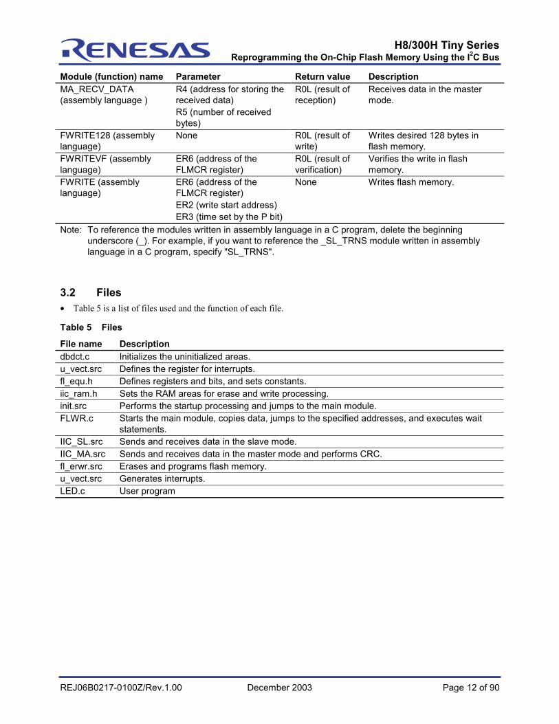
3.1 Modules• Table 4 is a list of modules used (parameters and return values).
Table 4 Modules
Module (function) name Parameter Return value DescriptionINIT (assembly language) None None Sets the stack pointer (sets R7
to H'FF80), sets CCR (disablesinterrupts), and jumps to themain module.
main None None Main moduleflprg_cpy None None Copies the data between
0x0400 and 0x08FF to the areabetween 0xF780 and 0xFC7F.
jump_prog (assemblylanguage)
R0 (address of the jumpdestination)
None Jumps to R0.
wait limit (wait length) None Executes a wait statement._SL_TRANS (assemblylanguage)
None None Enables transmission andreception of data in the slavemode.
SL_RECV_DATA(assembly language)
R4 (address for storing thereceived data)R5 (number of receivedbytes)
R0L (result ofreception)
Receives data in the slavemode.
SL_SEND_DATA(assembly language)
R4 (address for storing thedata to be sent)R5 (number of sent bytes)
R0L (result oftransmission)
Sends data in the slave mode.
CAL_CRC16 (assemblylanguage)
R4 (address for storing thereceived data)
R0 (result ofCRC)
Performs CRC.
_IIC_TEST (assemblylanguage)
None None Erases or writes flash memory.
FL_ER_BLK (assemblylanguage)
R0H (specifies the block tobe erased)
R0L (result oferase)
Erases data from flash memory.
BLK1_ERASE (assemblylanguage)
ER6 (address of theFLMCR register)ER5 (address of the EBRregister)
R0L (result oferase)
Erases the target block in flashmemory.
FERASEVF (assemblylanguage)
ER6 (address of theFLMCR register)
R0L (result ofverification)
Verifies the erase in flashmemory.
FERASE (assemblylanguage)
ER6 (address of theFLMCR register)ER5 (address of the EBRregister)
None Erases the target block in flashmemory.
FL_WAIT (assemblylanguage)
R0 (wait length) None Executes a wait statement.
MA_SEND_DATA(assembly language)
R4 (address for storing thedata to be sent)R5 (number of sent bytes)
R0L (result oftransmission)
Sends data in the master mode.
H8/300H Tiny SeriesReprogramming the On-Chip Flash Memory Using the I2C Bus
REJ06B0217-0100Z/Rev.1.00 December 2003 Page 12 of 90
Module (function) name Parameter Return value DescriptionMA_RECV_DATA(assembly language )
R4 (address for storing thereceived data)R5 (number of receivedbytes)
R0L (result ofreception)
Receives data in the mastermode.
FWRITE128 (assemblylanguage)
None R0L (result ofwrite)
Writes desired 128 bytes inflash memory.
FWRITEVF (assemblylanguage)
ER6 (address of theFLMCR register)
R0L (result ofverification)
Verifies the write in flashmemory.
FWRITE (assemblylanguage)
ER6 (address of theFLMCR register)ER2 (write start address)ER3 (time set by the P bit)
None Writes flash memory.
Note: To reference the modules written in assembly language in a C program, delete the beginningunderscore (_). For example, if you want to reference the _SL_TRNS module written in assemblylanguage in a C program, specify "SL_TRNS".
3.2 Files• Table 5 is a list of files used and the function of each file.
Table 5 Files
File name Descriptiondbdct.c Initializes the uninitialized areas.u_vect.src Defines the register for interrupts.fl_equ.h Defines registers and bits, and sets constants.iic_ram.h Sets the RAM areas for erase and write processing.init.src Performs the startup processing and jumps to the main module.FLWR.c Starts the main module, copies data, jumps to the specified addresses, and executes wait
statements.IIC_SL.src Sends and receives data in the slave mode.IIC_MA.src Sends and receives data in the master mode and performs CRC.fl_erwr.src Erases and programs flash memory.u_vect.src Generates interrupts.LED.c User program
H8/300H Tiny SeriesReprogramming the On-Chip Flash Memory Using the I2C Bus
REJ06B0217-0100Z/Rev.1.00 December 2003 Page 13 of 90
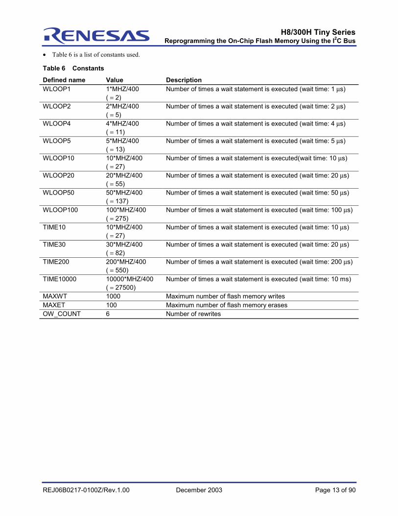
• Table 6 is a list of constants used.
Table 6 Constants
Defined name Value DescriptionWLOOP1 1*MHZ/400
( = 2)Number of times a wait statement is executed (wait time: 1 µs)
WLOOP2 2*MHZ/400( = 5)
Number of times a wait statement is executed (wait time: 2 µs)
WLOOP4 4*MHZ/400( = 11)
Number of times a wait statement is executed (wait time: 4 µs)
WLOOP5 5*MHZ/400( = 13)
Number of times a wait statement is executed (wait time: 5 µs)
WLOOP10 10*MHZ/400( = 27)
Number of times a wait statement is executed(wait time: 10 µs)
WLOOP20 20*MHZ/400( = 55)
Number of times a wait statement is executed (wait time: 20 µs)
WLOOP50 50*MHZ/400( = 137)
Number of times a wait statement is executed (wait time: 50 µs)
WLOOP100 100*MHZ/400( = 275)
Number of times a wait statement is executed (wait time: 100 µs)
TIME10 10*MHZ/400( = 27)
Number of times a wait statement is executed (wait time: 10 µs)
TIME30 30*MHZ/400( = 82)
Number of times a wait statement is executed (wait time: 20 µs)
TIME200 200*MHZ/400( = 550)
Number of times a wait statement is executed (wait time: 200 µs)
TIME10000 10000*MHZ/400( = 27500)
Number of times a wait statement is executed (wait time: 10 ms)
MAXWT 1000 Maximum number of flash memory writesMAXET 100 Maximum number of flash memory erasesOW_COUNT 6 Number of rewrites
H8/300H Tiny SeriesReprogramming the On-Chip Flash Memory Using the I2C Bus
REJ06B0217-0100Z/Rev.1.00 December 2003 Page 14 of 90
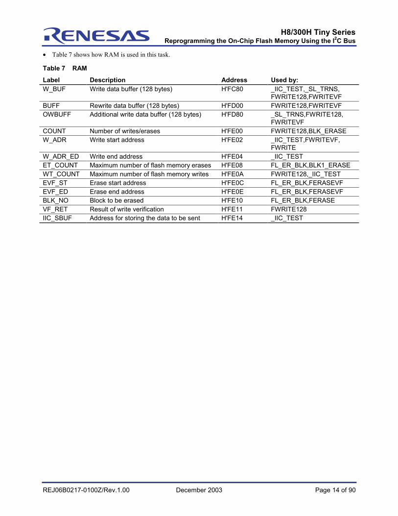
• Table 7 shows how RAM is used in this task.
Table 7 RAM
Label Description Address Used by:W_BUF Write data buffer (128 bytes) H'FC80 _IIC_TEST,_SL_TRNS,
FWRITE128,FWRITEVFBUFF Rewrite data buffer (128 bytes) H'FD00 FWRITE128,FWRITEVFOWBUFF Additional write data buffer (128 bytes) H'FD80 _SL_TRNS,FWRITE128,
FWRITEVFCOUNT Number of writes/erases H'FE00 FWRITE128,BLK_ERASEW_ADR Write start address H'FE02 _IIC_TEST,FWRITEVF,
FWRITEW_ADR_ED Write end address H'FE04 _IIC_TESTET_COUNT Maximum number of flash memory erases H'FE08 FL_ER_BLK,BLK1_ERASEWT_COUNT Maximum number of flash memory writes H'FE0A FWRITE128,_IIC_TESTEVF_ST Erase start address H'FE0C FL_ER_BLK,FERASEVFEVF_ED Erase end address H'FE0E FL_ER_BLK,FERASEVFBLK_NO Block to be erased H'FE10 FL_ER_BLK,FERASEVF_RET Result of write verification H'FE11 FWRITE128IIC_SBUF Address for storing the data to be sent H'FE14 _IIC_TEST

H8/300H Tiny SeriesReprogramming the On-Chip Flash Memory Using the I2C Bus
REJ06B0217-0100Z/Rev.1.00 December 2003 Page 15 of 90
• Table 8 shows the registers in RAM used.
Table 8 Registers in RAM
Register Description Availableaction
Set value
ICDR Stores the data to be sent or received data. Store andreference
―
MLS Sets data transmission beginning with the MSB. Set 0WAIT Sets continuous transmission of data and
acknowledge bits.Set 0
CKS2toCKS0
Sets the transmission clock frequency to 400 kHzwhen these bits are set together with the IICX bit ofSTCR.
Set CKS2 = 0CSK1 = 0CSK0 = 1
ICMR
BC2toBC0
Sets the number of bits in the data to be transferrednext in the I2C bus format to 9 bits per frame.
Set BC2 = 0BC1 = 0BC0 = 0
ICE Controls the access to ICMR, ICDR, SAR and SARXregisters, and selects whether to activate the I2C bus(SCL/SDA pins are used as ports ) or deactivate theI2C bus (SCL/SDA pins are driven by the bus).
Set 0/1
IEIC Disables interrupt requests over the I2C bus. Set 0/1MST Uses the I2C bus in the master mode. Set 0/1TRS Uses the I2C bus in the transmission mode. Set 0/1ACKE Cancels consecutive transmission when the
acknowledge bit is set to 1.Set 0/1
BBSY Checks whether the I2C bus is occupied or releasedand issues the start or stop condition when this bit isset together with the SCP bit.
Set andreference
0/1
IRIC Detects the start condition, determines the end ofdata transmission, and detects that the acknowledgebit is set to 1.
Set 0/1
ICCR
SCP Issues the start or stop condition when this bit is settogether with the BBSY bit.
Set 0/1
ESTP Flag for detecting the abnormal stop condition(enabled in the slave mode)
None ―
STOP Flag for detecting the normal stop condition (enabledin the slave mode)
None ―
IRTR Flag for consecutive transmission or receptioninterrupt requests
None ―
AASX Flag for acknowledging the second slave address None ―AL Flag for the lost arbitration None ―AAS Flag for acknowledging the slave address None ―ADZ Flag for acknowledging the general call address None ―
ICSR
ACKB Stores the acknowledge data sent from EEPROM. Reference ―IICRST Resets the IIC control module. Set 0TSCRIICX Selects the transmission rate. Set 0
FLMCR1 SWE Enables writing or erasing flash memory when SWEis set to 1.
Set 0/1
ESU Sets the erase preparation mode when ESU is set to1 and cancels the mode when ESU is cleared to 0.
Set 0/1

H8/300H Tiny SeriesReprogramming the On-Chip Flash Memory Using the I2C Bus
REJ06B0217-0100Z/Rev.1.00 December 2003 Page 16 of 90
Register Description Availableaction
Set value
PSU Sets the write preparation mode when PSU is set to1 and cancels the mode when PSU is cleared to 0.
Set 0/1
EV Sets the erase verification mode when EV is set to 1and cancels the mode when EV is cleared to 0.
Set 0/1
PV Sets the write verification mode when PV is set to 1and cancels the mode when PV is cleared to 0.
Set 0/1
E Sets the erase mode when SWE, ESU, and E areset to 1 and cancels the mode when E is cleared to0.
Set 0/1
P Sets the write mode when SWE, PSU, and P are setto 1 and cancels the mode when P is cleared to 0.
Set 0/1
EBR1 EB4 toEB0
Sets 28 kbytes between H'1000 and H'7FFF as theblocks to be erased in flash memory.
Set EB4 to EB0 =H'10
FENR FLSHE Enables the FLMCR1 and EBR1 registers. Set 0/1B6WI Validates the value of TCWE only when the value is
written when B6WI is cleared to 0. When the value ofTCWE is read, B6WI is fixed to 1.
Set 0/1
TCWE Validates the value written in the TCWD registerwhen TCWE is set to 1.
Set 1
B4WI Validates the value of TCSRWE only when the valueis written when B4WI is cleared to 0. When the valueof TCSRWE is read, B4WI is fixed to 1.
Set 0/1
TCSRWE Validates the values of the WDON and WRST bitswhen TCSRWE is set to 1.
Set 1
B2WI Validates the value of WDON only when the value iswritten when B2WI is cleared to 0. When the value ofWDON is read, B2WI is fixed to 1.
Set 0/1
TCWE Counts up TCWD when WDON is set to 1. StopsTCWD when WDON is cleared to 0.
Set 0/1
B0WI Validates the value of WRST only when the value iswritten when B0WI is cleared to 0. When the value ofWRST is read, B0WI is fixed to 1.
Set 0/1
TCSRWD
TCSRWE Resets the watchdog timer. Set 1TMWD CKS3
toCKS0
Selects the clock signal to be input to TCWD.CKS 3 to CKS 0 = H'8: Internal clock signal (φ)/64CKS 3 to CKS 0 = H'D: Internal clock signal (φ)/2048
Set CKS3 toCKS0 =H'8 or H'D
TCWD 8-bit count register that can be read and written Set 166 or100

H8/300H Tiny SeriesReprogramming the On-Chip Flash Memory Using the I2C Bus
REJ06B0217-0100Z/Rev.1.00 December 2003 Page 17 of 90
3.3 Defining sections• Table 9 shows the sections defined in this task.
Table 9 Defined Sections
Address Section DescriptionH'0000 V0 Vector address for such as RESETH'0010 V1 Vector address for such as TRAPH'002E V2 Vector address for such as SCIH'0040 PM Program areaH'0400 PF_1 Program areaH'0900 PF_2 Program areaH'1000 UV User vector table areaH'1100 P User program area
C$DSEC Initialized data area (defined in DBSCT.C)C$BSEC Uninitiaized data area (defined in DBSCT.C)D Initialized data area
H'FE80 B Uninitiaized data areaR Initialized data area
H8/300H Tiny SeriesReprogramming the On-Chip Flash Memory Using the I2C Bus
REJ06B0217-0100Z/Rev.1.00 December 2003 Page 18 of 90
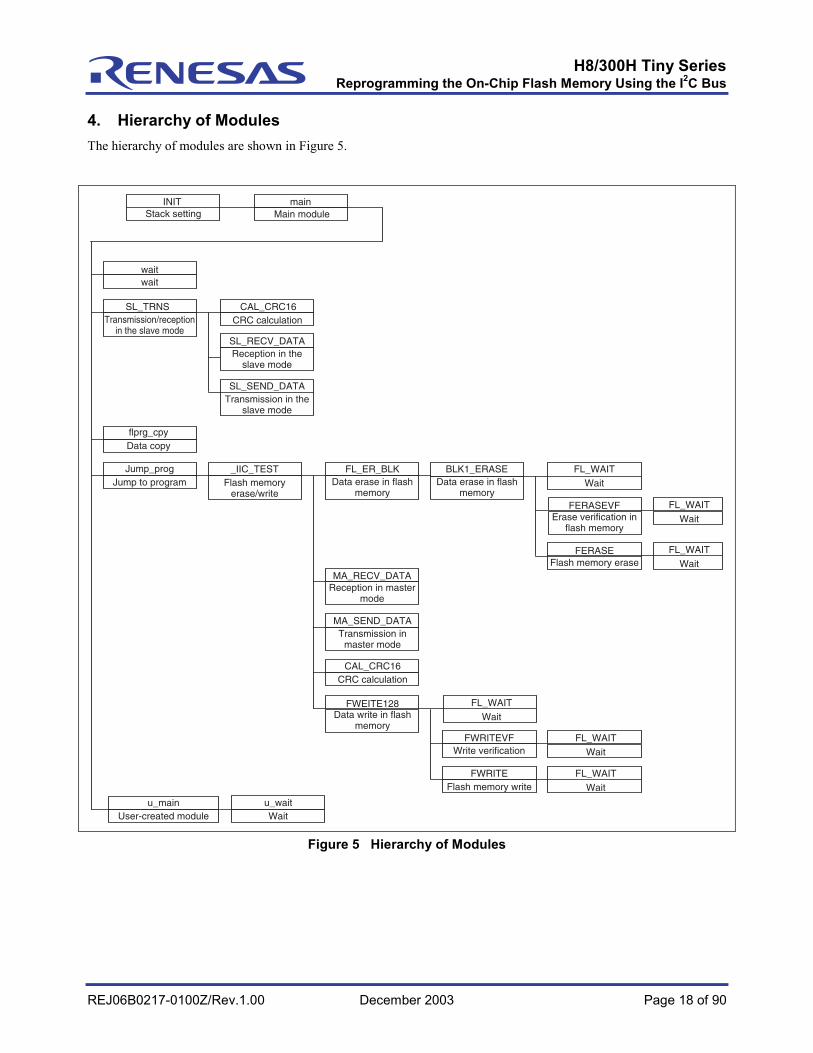
4. Hierarchy of ModulesThe hierarchy of modules are shown in Figure 5.
INIT main
SL_TRNS CAL_CRC16
SL_RECV_DATA
waitwait
CRC calculation
SL_SEND_DATA
flprg_cpy
Jump_prog _IIC_TEST FL_ER_BLK
MA_RECV_DATA
BLK1_ERASE
FERASEVF
FERASE
MA_SEND_DATA
FWEITE128
CAL_CRC16
FWRITEVF
FWRITE
u_main u_wait
Stack setting Main module
Transmission/reception in the slave mode
Reception in the slave mode
Transmission in the slave mode
Flash memory erase/write
Data erase in flash memory
Reception in master mode
Transmission in master mode
Data write in flash memory
Data erase in flash memory
Flash memory erase
CRC calculation
Erase verification in flash memory
Data copy
Jump to programFL_WAIT
Wait
FL_WAIT
Wait
FL_WAIT
Wait
FL_WAIT
Wait
Write verification
Flash memory write
FL_WAIT
Wait
FL_WAIT
Wait
User-created module Wait
Figure 5 Hierarchy of Modules

H8/300H Tiny SeriesReprogramming the On-Chip Flash Memory Using the I2C Bus
REJ06B0217-0100Z/Rev.1.00 December 2003 Page 19 of 90
5. Flowcharts
No
Yes
No
YesNo
Yes
No
Yes
INIT
Jump to main.
main
rts
i < 500?
SL_TRNS
sw_d1 = 0x20?
flprg_cpy
u_main
sw_d1 = sw_d2?
sw_d1 = 0x10?
Set the stack pointer to H'FF80.
Set PCR5 to 0x00.
Set PDR8 to 0x00.
wait (parameter: 10000)
Set PDR8 to 0x10.
Increment i.
wait (parameter: 10000)
jump_prog (parameter: 0xF780)
Set the result of ((PDR5 & 0x20)|(PDR1 & 0x10)) in swd1.
Set the result of ((PDR5 & 0x20)|(PDR1 & 0x10)) in swd2.
Set PCR1 to 0x00.
Set PDR8 to 0x00.
Set PCR8 to 0x10.
Clear i to 0.
Set the I bit to 1 and reject serial interrupts.

H8/300H Tiny SeriesReprogramming the On-Chip Flash Memory Using the I2C Bus
REJ06B0217-0100Z/Rev.1.00 December 2003 Page 20 of 90
Yes
No
flprg_cpy
rts
ptr <0x0900?
Set ptr to 0x04000.
jump_prog (parameter: R0)
Jump to R0.
Write *ptr in *r_ptr.
Increment ptr.
Increment r_ptr.
Set r_ptr to 0xF780.
Note: Use a compiler to set the beginning of _IIC_TEST to 0x0400, use flprg_cpy to write the copy after0xF780, and use jump_prog to execute the copy.

H8/300H Tiny SeriesReprogramming the On-Chip Flash Memory Using the I2C Bus
REJ06B0217-0100Z/Rev.1.00 December 2003 Page 21 of 90
Yes
Nocnt <limit?
rts
wait (parameter: limit)
Clear cnt to 0.
Increment cnt.
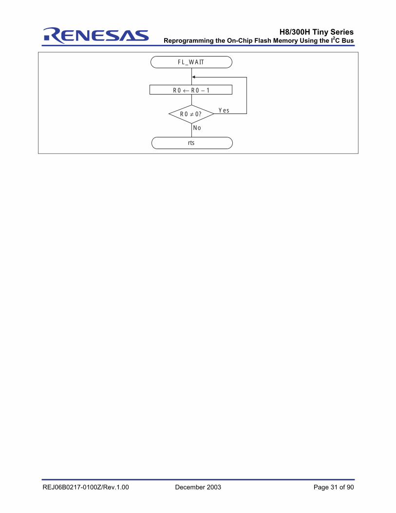
H8/300H Tiny SeriesReprogramming the On-Chip Flash Memory Using the I2C Bus
REJ06B0217-0100Z/Rev.1.00 December 2003 Page 22 of 90
No
Yes
No
Yes
No
No
Yes
Yes
Yes
No
SL_RECV_DATA
CAL_CRC16
SL_SEND_DATA
R0L = 0?
R0L = 0?
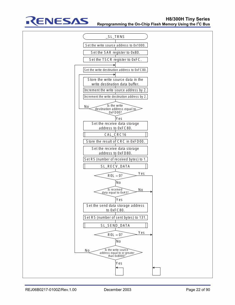
_SL_TRNS
Set the write source address to 0x1000.
Set the SAR register to 0x80.
Is the write destination address equal to
0xFD00?
Is received data equal to 0xA5?
Is the write source address equal to or greater
than 0x8000?
Set the TSCR register to 0xFC.
Store the result of CRC in 0xFD00.
Set R5 (number of received bytes) to 1.
Set R5 (number of sent bytes) to 131.
Increment the write destination address by 2.
Increment the write source address by 2.
Store the write source data in the write destination data buffer.
Set the receive data storage address to 0xFC80.
Set the receive data storage address to 0xFD80.
Set the send data storage address to 0xFC80.
Set the write destination address to 0xFC80.
H8/300H Tiny SeriesReprogramming the On-Chip Flash Memory Using the I2C Bus
REJ06B0217-0100Z/Rev.1.00 December 2003 Page 23 of 90
Yes
No
Yes
No
No
Yes
No
Yes
Yes
No
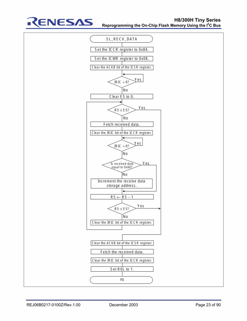
SL_RECV_DATA
IRIC = 0?
R5 ≤ E5?
R5 ≤ E5?
rts
IRIC = 0?
Set the ICCR register to 0x84.
Set the ICMR register to 0x08.
Clear E5 to 0.
Fetch received data.
Is received data equal to 0x80?
Clear the IRIC bit of the ICCR register.
Clear the IRIC bit of the ICCR register.
Clear the ACKB bit of the ICSR register.
Fetch the received data.
Set R0L to 1.
Clear the IRIC bit of the ICCR register.
R5 ← R5 − 1
Increment the receive data storage address.
Clear the ACKB bit of the ICSR register.

H8/300H Tiny SeriesReprogramming the On-Chip Flash Memory Using the I2C Bus
REJ06B0217-0100Z/Rev.1.00 December 2003 Page 24 of 90
No
rts
Yes
No
Yes
No
1-1
Yes
No
Yes
No
1-1
Yes
No
Yes
SL_SEND_DATA
R0 = 40?
ACKB = 0?
ACKB = 0?
IRIC = 0?
AND the value of the ICCR register and 0xFE, OR the result and 0x04, and
store the result in the ICCR register.
OR the value of the ICCR register and 0x10 and store the result in the
ICCR register.
Clear the IRIC bit of the ICCR register.
Store the data to be sent in ICDR.
Clear the IRIC bit of the ICCR register.
Set E5 to 1.
Store the data to be sent in ICDR.
Increment the send data address.
Clear R0L to 0.
Clear R0 to 0.
Increment R0.
Set R0L to 1.
Set the ICDR register as R1L.
Clear the TRS bit of the ICCR register.
Clear the IRIC bit of the ICCR register.
R5 ≤ E5?
IRIC = 0?
E5 ← E5 + 1
AND the value of the ICCR register and 0xFA and store the result in the
ICCR register.

H8/300H Tiny SeriesReprogramming the On-Chip Flash Memory Using the I2C Bus
REJ06B0217-0100Z/Rev.1.00 December 2003 Page 25 of 90
Yes
No
Yes
No
Yes
No
rts
CAL_CRC16
E0 = 8?
E1 = 0?
Clear E5 to 0.
Set E1 to 128.
Clear R1H to 0.
Left-shift R1 by 8 bits.
Clear E0 to 0.
Left-shift E5 by 1 bit.
Left-shift R1 by 1 bit.
Increment E0.
Store the result of CRC in R0.
Left-shift E5 by 1 bit.
Increment the receive data address.
XOR the value of E5 and 0x1021 and store the result in E5.
Store the received data in R1L.
R1 xor E5 > 0?
E1 ← E1 − 1

H8/300H Tiny SeriesReprogramming the On-Chip Flash Memory Using the I2C Bus
REJ06B0217-0100Z/Rev.1.00 December 2003 Page 26 of 90
No
No
Yes
Yes
No
No
Yes
CAL_CRC16
MA_SEND_DATA
_IIC_TEST
FL_ER_BLK
Yes
R0L = 0?
MA_RECV_DATA
2-3
2-1
2-2
Yes
No
Yes
No
No
YesR2 < R3?
FWRITE128
R0L = 0?
R1 = R0? 2-2
2-4
2-1
2-2
2-3
2-4
Store the value of the FENR register in R6 and set the FLSHE bit.
Set R0H to 0x10.
Set the write start address to 0x1000.
Set the write end address to 0x8000.
Set MAXWT as the maximum number of writes.
Set R5 to 1.
Set R1 to 30.
Set R5 to 131.
Set the receive data storage address to 0xFC80.
Set the receive data storage address to 0xFC80. Store the value of the FENR
register in R6 and clear the FLSHE bit.
Set the send data storage address to 0xFE14 and store the data to be sent in 0xA5.
Set the data at 0xFD00 in R1.
Increment the write start address by 128 and store the
address in R2.
Store the write end address in R3.
R0L = 0?
R1 = 0?
R0L = 0?
R1 ← R1 − 1

H8/300H Tiny SeriesReprogramming the On-Chip Flash Memory Using the I2C Bus
REJ06B0217-0100Z/Rev.1.00 December 2003 Page 27 of 90
Yes
Yes
No
No
Yes
No
BLK1_ERASE
FR_ER_BLK
rts
R0L = 0?
rts
R0H= 0x08?
R0H= 0x10?
Set R1 to 0x0C00.
Set R1 to 0x1000.
Set R2 to 0x8000.
Set R0L to 1.
Set R2 to 0x1000.
Set R0H as the block to be erased.
Set R1 as the start address to be erased.
Set R2 as the end address to be erased.
Set the address of EBR1 (0xFF93) in R5.
Set the address of FLMCR1 (0xFF90) in R6.
Set MAXET as the maximum number of erases.
H8/300H Tiny SeriesReprogramming the On-Chip Flash Memory Using the I2C Bus
REJ06B0217-0100Z/Rev.1.00 December 2003 Page 28 of 90
No
Yes
rts rts
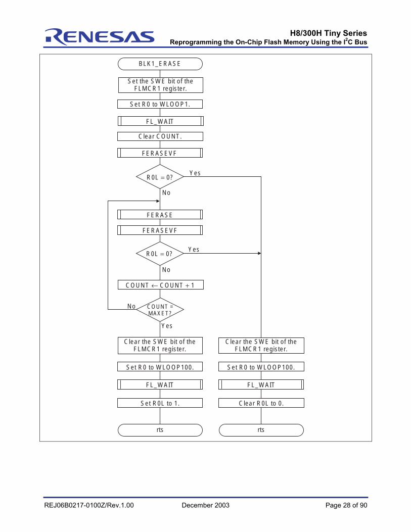
COUNT ← COUNT + 1
No
FL_WAIT FL_WAIT
Yes
BLK1_ERASE
FERASE
FL_WAIT
FERASEVF
R0L = 0?
FERASEVF
No
YesR0L = 0?
Set the SWE bit of the FLMCR1 register.
Set R0 to WLOOP1.
Clear COUNT.
COUNT = MAXET?
Clear the SWE bit of the FLMCR1 register.
Clear the SWE bit of the FLMCR1 register.
Set R0 to WLOOP100. Set R0 to WLOOP100.
Set R0L to 1. Clear R0L to 0.

H8/300H Tiny SeriesReprogramming the On-Chip Flash Memory Using the I2C Bus
REJ06B0217-0100Z/Rev.1.00 December 2003 Page 29 of 90
No
Yes
No
FL_WAIT
Yes
rtsrts
FL_WAIT
Set the verification start address as the address to
be verified.
FL_WAIT
FERASEVF
FL_WAIT
Set the EV bit of the FLMCR register.
Write dummy data (0xFFFF) at the address to be verified.
Increment the verification start address.
Clear the EV bit of the FLMCR register.
Set R0 to WLOOP4.
Set R0L to 1. Clear R0L to 0.
Set R0 to WLOOP4.
Clear the EV bit of the FLMCR register.
Is verification data equal to
0xFFFF?
Is this the last address to be
verified?
Set R0 to WLOOP20.
Set R0 to WLOOP2.
H8/300H Tiny SeriesReprogramming the On-Chip Flash Memory Using the I2C Bus
REJ06B0217-0100Z/Rev.1.00 December 2003 Page 30 of 90
Yes
No
FL_WAIT
FL_WAIT
FL_WAIT
rts
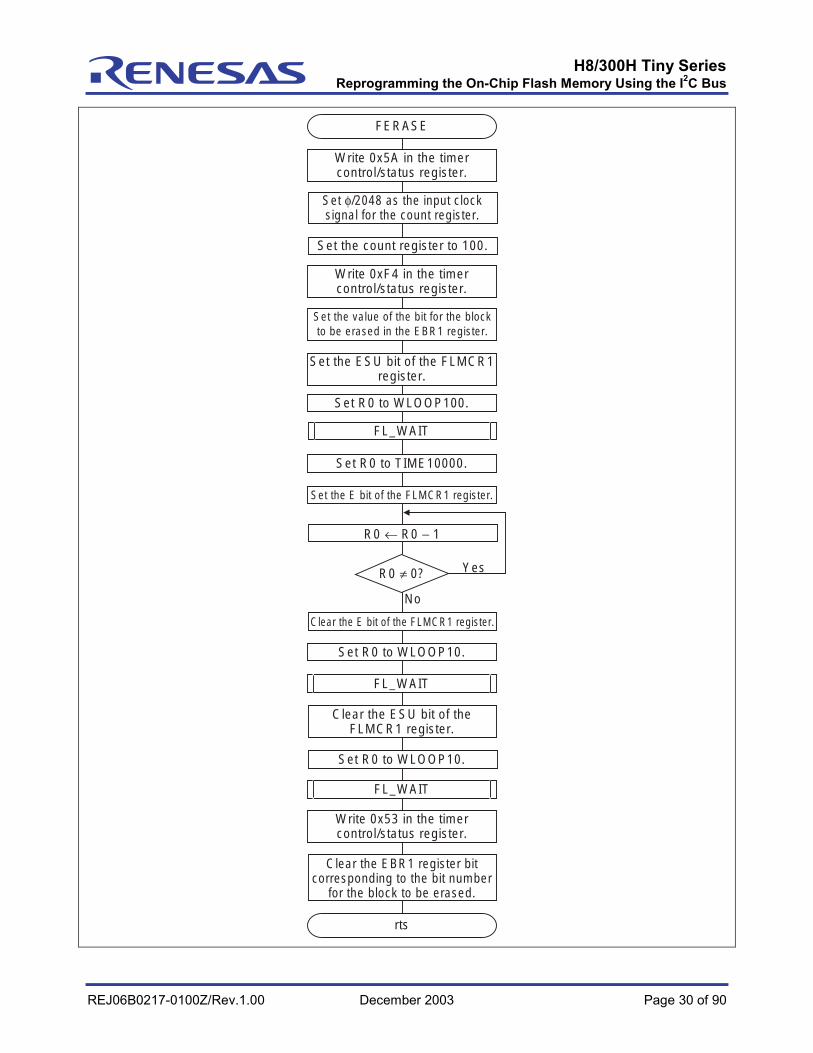
FERASE
R0 ← R0 − 1
R0 ≠ 0?
Write 0x5A in the timer control/status register.
Write 0xF4 in the timer control/status register.
Set the ESU bit of the FLMCR1 register.
Clear the ESU bit of the FLMCR1 register.
Write 0x53 in the timer control/status register.
Clear the EBR1 register bit corresponding to the bit number
for the block to be erased.
Set the value of the bit for the block to be erased in the EBR1 register.
Set the count register to 100.
Set R0 to WLOOP100.
Set R0 to TIME10000.
Set R0 to WLOOP10.
Set R0 to WLOOP10.
Clear the E bit of the FLMCR1 register.
Set the E bit of the FLMCR1 register.
Set φ/2048 as the input clock signal for the count register.
H8/300H Tiny SeriesReprogramming the On-Chip Flash Memory Using the I2C Bus
REJ06B0217-0100Z/Rev.1.00 December 2003 Page 31 of 90
Yes
No
FL_WAIT
rts
R0 ← R0 − 1
R0 ≠ 0?

H8/300H Tiny SeriesReprogramming the On-Chip Flash Memory Using the I2C Bus
REJ06B0217-0100Z/Rev.1.00 December 2003 Page 32 of 90
Yes
No
Yes
No
Yes
No
Yes
No
Yes
No
Yes
No
Yes
No
3-1
3-1
MA_SEND_DATA
rts
R5 ≤ E5?
ACKB = 0?
ACKB = 0?
BBSY = 0?
IRIC = 0?
IRIC = 0?
Set the ICCR register to 0x89.
Set the ICMR register to 0x08.
Set the TSCR register to 0xFC.
Set the ICDR register to 0x80.
Clear the IRIC bit of the ICCR register.
Clear E5 to 0.
Store the data to be sent in ICDR.
Increment the send data address.
Increment E5.
Clear R0L to 0. Set R0L to 1.
Clear the IRIC bit of the ICCR register.
OR the value of the ICCR register and 0x30 and store the result in the ICCR register.
AND the value of the ICCR register and 0xFE, OR the result and 0x04, and store the result in the ICCR register.
IRIC = 0?
H8/300H Tiny SeriesReprogramming the On-Chip Flash Memory Using the I2C Bus
REJ06B0217-0100Z/Rev.1.00 December 2003 Page 33 of 90
Yes
No
Yes
No
Yes
No
Yes
No
Yes
No
Yes
No
Yes
No
rts
R5 ≤ E5?
R5 = R6?
IRIC = 0?
IRIC = 0?
IRIC = 0?
IRIC = 0?
MA_RECV_DATA
R5 ← R5 − 1
Store the value of R5 in R6.
Clear the TRS bit of the ICCR register.
Set the WAIT bit of the ICMR register.
Fetch the received data.
Clear the IRIC bit of the ICCR register.
Clear the IRIC bit of the ICCR register.
Set E5 to 1.
Fetch the received data.Set the ACKB bit of the ICSR register.
Set the TRS bit of the ICCR register.
Clear the IRIC bit of the ICCR register.
Clear the WAIT bit of the ICMR register.
Fetch the received data.
Clear the IRIC bit of the ICCR register.
Set R0L to 1.
AND the value of the ICCR register and 0xFA and store the result in the
ICCR register.
Clear the IRIC bit of the ICCR register.
Increment the receive data address.
Clear the IRIC bit of the ICCR register.
Clear the ACKB bit of the ICSR register.
R5 ≤ E5?

H8/300H Tiny SeriesReprogramming the On-Chip Flash Memory Using the I2C Bus
REJ06B0217-0100Z/Rev.1.00 December 2003 Page 34 of 90
No
Yes
No
Yes
No
Yes
No
Yes
No
Yes
No
Yes
No
Yes
Yes
No
4-2
4-1
4-2
4-24-1
4-2
4-1
4-1
FL_WAITFL_WAIT
FWRITEVF
FWRITE
FWRITEVF
FWRITE
FWRITE
FL_WAIT
FWRITEVF
rts rts
FWRITE128
R0L = 0?
R0L = 2?
R0L = 0?
R0L = 2?
VF_RET = 2?
VF_RET = 0?
Transfer 128 bytes of write data to the rewrite data buffer.
Set the SWE bit of the FLMCR1 register.
Set BUFF as the write address.
Set BUFF as the write address.
Store the result of verification in VF_RET.
Set OWBUFF as the write address.
Set R0 to WLOOP1.
Clear COUNT.
Set R3 to TIME200.
Increment COUNT.
Set R0 to WLOOP100. Set R0 to WLOOP100.
Set R0L to 1. Clear R0L to 0.
Set R3 to TIME30.
Set R3 to TIME10.
Increment COUNT.
COUNT = OW_COUNT?
COUNT = WT_COUNT?
Clear the SWE bit of the FLMCR1 register.
Clear the SWE bit of the FLMCR1 register.

H8/300H Tiny SeriesReprogramming the On-Chip Flash Memory Using the I2C Bus
REJ06B0217-0100Z/Rev.1.00 December 2003 Page 35 of 90
Yes
No
No
Yes
Yes
No
No
Yes
FL_WAIT
FL_WAIT
FL_WAIT
FL_WAIT
rtsrts
FWRITEVF
R0 ≠ 0?
E0 = 0xFFFF?
Set BUFF as the rewrite address.
Set the PV bit of the FLMCR1 register.
Set W_BUF as the write address.
Set R0 to WLOOP4.
Set R0 to WLOOP2.
Set R0 to WLOOP2.
Set R0L to 1.
Set BUFF as the rewrite address.
Store rewrite data in E0.
Clear R0L to 0.
Clear the PV bit of the FLMCR1 register.
Clear the PV bit of the FLMCR1 register.
Set R0 to WLOOP2.
Set R0L to 2.
Set W_ADR as the flash memory write address.
Set OWBUFF as the additional write address.
Write dummy data (0xFFFF) in flash memory. Is the write address
equal to W_BUF + 128?
Is the rewrite address equal to BUFF +
128?
Increment the additional write address by 2.
Increment the rewrite address by 2.
Increment the flash memory write address.
Increment the rewrite data address.
Increment the write data address.
OR the inverse of flash memory data and write data, and store
the result in R0.
OR flash memory data and rewrite data, and write the result in the additional write data buffer.
OR the inverse of flash memory data and write data, and write the result in the rewrite data buffer.

H8/300H Tiny SeriesReprogramming the On-Chip Flash Memory Using the I2C Bus
REJ06B0217-0100Z/Rev.1.00 December 2003 Page 36 of 90
Yes
No
Yes
No
FL_WAIT
FL_WAIT
FL_WAIT
rts
FWRITE
R3 ← R3 − 1
E0 ← E0 − 1
R0 ≠ 0?
E0 ≠ 0?
Set E0 to 128.
Write the data of the write source address to the write
destination address.
Increment the write source address.
Increment the write destination address.
Set the count register to 166.
Set R0 to WLOOP50.
Set the P bit of the FLMCR1 register.
Clear the P bit of the FLMCR1 register.
Set R0 to WLOOP5.
Set R0 to WLOOP5.
Write 0x5A in the timer control/status register.
Write 0xF4 in the timer control/status register.
Set the PSU bit of the FLMCR1 register.
Clear the PSU bit of the FLMCR1 register.
Write 0x53 in the timer control/status register.
Set φ/64 as the input clock signal for the count register.

H8/300H Tiny SeriesReprogramming the On-Chip Flash Memory Using the I2C Bus
REJ06B0217-0100Z/Rev.1.00 December 2003 Page 37 of 90
Trap instructions #1 to #4
Jump to INIT.
Break condition interrupt Sleep instruction interrupt
IRQ #1 to #4 interrupt WKP interrupt
Overflow interrupt Timer (W, V) interrupt
I2C interrupt
SCI interrupt
A/D conversion interrupt

H8/300H Tiny SeriesReprogramming the On-Chip Flash Memory Using the I2C Bus
REJ06B0217-0100Z/Rev.1.00 December 2003 Page 38 of 90
6. Description of Software
6.1 Modules• Table 10 explains the modules used (parameters and return values).
Table 10 Modules
Module (function)name
Parameter Return value Description
INIT (assemblylanguage)
None None Sets the stack pointer (sets R7 toH'FF80), sets CCR (disablesinterrupts), and jumps to the mainmodule.
main None None Main moduleflprg_cpy None None Copies the data between 0x0400 and
0x08FF to the area between 0xF780and 0xFC7F.
jump_prog(assembly language)
R0 None The program jumps to R0.
wait limit (wait length) None Executes a wait statement._SL_TRANS(assembly language)
None None Enables transmission and reception ofdata in the slave mode.
SL_RECV_DATA(assembly language)
R4 (address for storing thereceived data)R5 (number of receivedbytes)
R0L (result ofreception)
Receives data in the slave mode.
SL_SEND_DATA(assembly language)
R4 (address for storing thedata to be sent)R5 (number of sent bytes)
ROL (resultoftransmission)
Sends data in the slave mode.
CAL_CRC16(assembly language)
R4 (address for storing thereceived data)
R0 (result ofCRC)
Performs CRC.
_IIC_TEST(assembly language)
None None Erases or writes flash memory.
FL_ER_BLK(assembly language)
R0H (specifies the block tobe erased)
R0L (result oferasing)
Erases data from flash memory.
BLK1_ERASE(assembly language)
ER6 (address of theFLMCR register)ER5 (address of the EBRregister)
R0L (result oferasing)
Erases the target block in flashmemory.
FERASEVF(assembly language)
ER6 (address of theFLMCR register)
R0L (result ofverification)
Verifies the erase in flash memory.
FERASE (assemblylanguage)
ER6 (address of theFLMCR register)ER5 (address of the EBRregister)
R0L (result oferasing)
Erases the target block in flashmemory.
FL_WAIT (assemblylanguage)
R0 (wait length) None Executes a wait statement.
MA_SEND_DATA(assembly language)
R4 (address for storing thedata to be sent)R5 (number of sent bytes)
R0L (result oftransmission)
Sends data in the master mode.

H8/300H Tiny SeriesReprogramming the On-Chip Flash Memory Using the I2C Bus
REJ06B0217-0100Z/Rev.1.00 December 2003 Page 39 of 90
Module (function)name
Parameter Return value Description
MA_RECV_DATA(assembly language)
R4 (address for storing thereceived data)R5 (number of receivedbytes)
R0L (result ofreception)
Receives data in the master mode.
FWRITE128(assembly language)
None R0L (result ofwriting)
Writes desired 128 bytes in flashmemory.
FWRITEVF(assembly language)
ER6 (address of theFLMCR register)
R0L (result ofverification)
Verifies the write in flash memory.
FWRITE (assemblylanguage)
ER6 (address of theFLMCR register)ER2 (write start address)ER3 (time set by the P bit)
None Writes flash memory.
Note: To reference the modules written in assembly language in a C program, delete the beginningunderscore (_). For example, if you want to reference the _SL_TRNS module written in assemblylanguage in a C program, specify "SL_TRNS".
H8/300H Tiny SeriesReprogramming the On-Chip Flash Memory Using the I2C Bus
REJ06B0217-0100Z/Rev.1.00 December 2003 Page 40 of 90
• Table 11 is a list of constants used.
Table 11 Constants
Defined name Value DescriptionWLOOP1 1*MHZ/400
( = 2)Number of times a wait statement is executed (wait time: 1 µs)
WLOOP2 2*MHZ/400( = 5)
Number of times a wait statement is executed (wait time: 2 µs)
WLOOP4 4*MHZ/400( = 11)
Number of times a wait statement is executed (wait time: 4 µs)
WLOOP5 5*MHZ/400( = 13)
Number of times a wait statement is executed (wait time: 5 µs)
WLOOP10 10*MHZ/400( = 27)
Number of times a wait statement is executed (wait time: 10 µs)
WLOOP20 20*MHZ/400( = 55)
Number of times a wait statement is executed (wait time: 20 µs)
WLOOP50 50*MHZ/400( = 137)
Number of times a wait statement is executed (wait time: 4 µs)
WLOOP100 100*MHZ/400( = 275)
Number of times a wait statement is executed (wait time: 5 µs)
TIME10 10*MHZ/400( = 27)
Number of times a wait statement is executed (wait time: 10 µs)
TIME30 30*MHZ/400( = 82)
Number of times a wait statement is executed (wait time: 20 µs)
TIME200 200*MHZ/400( = 550)
Number of times a wait statement is executed (wait time: 200µs)
TIME10000 10000*MHZ/400( = 27500)
Number of times a wait statement is executed (wait time: 10 ms)
MAXWT 1000 Maximum number of flash memory writesMAXET 100 Maximum number of flash memory erasesOW_COUNT 6 Number of rewrites

H8/300H Tiny SeriesReprogramming the On-Chip Flash Memory Using the I2C Bus
REJ06B0217-0100Z/Rev.1.00 December 2003 Page 41 of 90
• Table 12 shows how RAM is used.
Table 12 RAM
Label Description Address Used by:W_BUF Write data buffer (128 bytes) H'FC80 _IIC_TEST,_SL_TRNS,
FWRITE128,FWRITEVFBUFF Rewrite data buffer (128 bytes) H'FD00 FWRITE128,FWRITEVFOWBUFF Additional write data buffer (128 bytes) H'FD80 _SL_TRNS,FWRITE128,
FWRITEVFCOUNT Number of writes/erases H'FE00 FWRITE128,BLK_ERASEW_ADR Write start address H'FE02 _IIC_TEST,FWRITEVF,
FWRITEW_ADR_ED Write end address H'FE04 _IIC_TESTET_COUNT Maximum number of flash memory erases H'FE08 FL_ER_BLK,BLK1_ERASEWT_COUNT Maximum number of flash memory writes H'FE0A FWRITE128,_IIC_TESTEVF_ST Erase start address H'FE0C FL_ER_BLK,FERASEVFEVF_ED Erase end address H'FE0E FL_ER_BLK,FERASEVFBLK_NO Block to be erased H'FE10 FL_ER_BLK,FERASEVF_RET Result of write verification H'FE11 FWRITE128IIC_SBUF Address for storing the data to be sent H'FE14 _IIC_TEST
H8/300H Tiny SeriesReprogramming the On-Chip Flash Memory Using the I2C Bus
REJ06B0217-0100Z/Rev.1.00 December 2003 Page 42 of 90
• Table 13 shows the registers in RAM.
Table 13 Registers in RAM
Register Description Availableaction
Set value
ICDR Stores the data to be sent or received. Store andreference
―
MLS Sets data transmission beginning with the MSB. Set 0WAIT Sets continuous transmission of data and
acknowledge bits.Set 0
CKS2toCKS0
Sets the transmission clock frequency to 400 kHzwhen these bits are set together with the IICX bit ofSTCR.
Set CKS2 = 0CSK1 = 0CSK0 = 1
ICMR
BC2toBC0
Sets the number of bits in the data to be transferrednext in the I2C bus format to 9 bits per frame.
Set BC2 = 0BC1 = 0BC0 = 0
ICE Controls the access to ICMR, ICDR, SAR and SARXregisters, and selects whether to activate the I2C bus(SCL/SDA pins are used as ports ) or deactivate theI2C bus (SCL/SDA pins are driven by the bus).
Set 0/1
IEIC Disables interrupt requests over the I2C bus. Set 0/1MST Uses the I2C bus in the master mode. Set 0/1TRS Uses the I2C bus in the transmission mode. Set 0/1ACKE Cancels consecutive transmission when the
acknowledge bit is set to 1.Set 0/1
BBSY Checks whether the I2C bus is occupied or releasedand issues the start or stop condition when this bit isset together with the SCP bit.
Set andreference
0/1
IRIC Detects the start condition, determines the end ofdata transmission, and detects that the acknowledgebit is set to 1.
Set 0/1
ICCR
SCP Issues the start or stop condition when this bit is settogether with the BBSY bit.
Set 0/1
ESTP Flag for detecting the abnormal stop condition(enabled in the slave mode)
None ―
STOP Flag for detecting the normal stop condition (enabledin the slave mode)
None ―
IRTR Flag for continuous transmission or receptioninterrupt requests
None ―
AASX Flag for acknowledging the second slave address None ―AL Flag for the lost arbitration None ―AAS Flag for acknowledging the slave address None ―ADZ Flag for acknowledging the general call address None ―
ICSR
ACKB Stores the acknowledge data sent from EEPROM. Reference ―IICRST Resets the IIC control module. Set 0TSCRIICX Selects the transmission rate. Set 0
FLMCR1 SWE Enables writing or erasing flash memory when SWEis set to 1.
Set 0/1
ESU Sets the erase preparation mode when ESU is set to1 and cancels the mode when ESU is cleared to 0.
Set 0/1
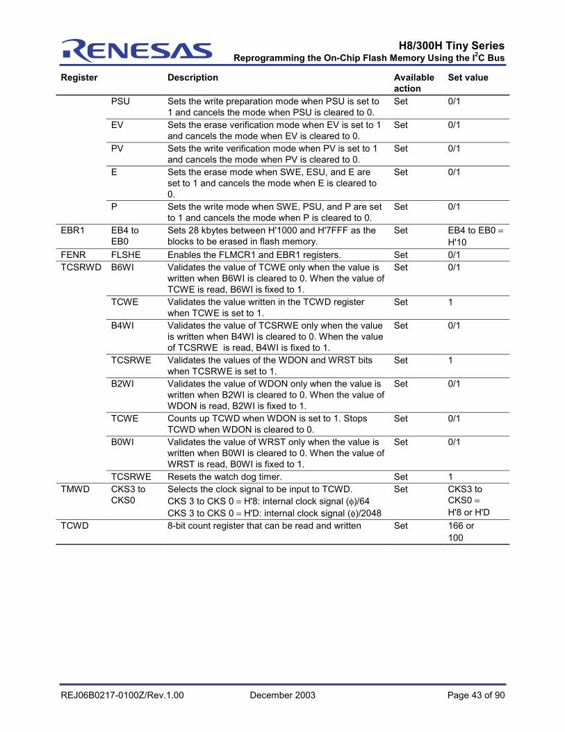
H8/300H Tiny SeriesReprogramming the On-Chip Flash Memory Using the I2C Bus
REJ06B0217-0100Z/Rev.1.00 December 2003 Page 43 of 90
Register Description Availableaction
Set value
PSU Sets the write preparation mode when PSU is set to1 and cancels the mode when PSU is cleared to 0.
Set 0/1
EV Sets the erase verification mode when EV is set to 1and cancels the mode when EV is cleared to 0.
Set 0/1
PV Sets the write verification mode when PV is set to 1and cancels the mode when PV is cleared to 0.
Set 0/1
E Sets the erase mode when SWE, ESU, and E areset to 1 and cancels the mode when E is cleared to0.
Set 0/1
P Sets the write mode when SWE, PSU, and P are setto 1 and cancels the mode when P is cleared to 0.
Set 0/1
EBR1 EB4 toEB0
Sets 28 kbytes between H'1000 and H'7FFF as theblocks to be erased in flash memory.
Set EB4 to EB0 =H'10
FENR FLSHE Enables the FLMCR1 and EBR1 registers. Set 0/1B6WI Validates the value of TCWE only when the value is
written when B6WI is cleared to 0. When the value ofTCWE is read, B6WI is fixed to 1.
Set 0/1
TCWE Validates the value written in the TCWD registerwhen TCWE is set to 1.
Set 1
B4WI Validates the value of TCSRWE only when the valueis written when B4WI is cleared to 0. When the valueof TCSRWE is read, B4WI is fixed to 1.
Set 0/1
TCSRWE Validates the values of the WDON and WRST bitswhen TCSRWE is set to 1.
Set 1
B2WI Validates the value of WDON only when the value iswritten when B2WI is cleared to 0. When the value ofWDON is read, B2WI is fixed to 1.
Set 0/1
TCWE Counts up TCWD when WDON is set to 1. StopsTCWD when WDON is cleared to 0.
Set 0/1
B0WI Validates the value of WRST only when the value iswritten when B0WI is cleared to 0. When the value ofWRST is read, B0WI is fixed to 1.
Set 0/1
TCSRWD
TCSRWE Resets the watch dog timer. Set 1TMWD CKS3 to
CKS0Selects the clock signal to be input to TCWD.CKS 3 to CKS 0 = H'8: internal clock signal (φ)/64CKS 3 to CKS 0 = H'D: internal clock signal (φ)/2048
Set CKS3 toCKS0 =H'8 or H'D
TCWD 8-bit count register that can be read and written Set 166 or100

H8/300H Tiny SeriesReprogramming the On-Chip Flash Memory Using the I2C Bus
REJ06B0217-0100Z/Rev.1.00 December 2003 Page 44 of 90
7. Hierarchy of Modules• Figure 6 shows the hierarchy of modules.
SL_TRNS CAL_CRC16
SL_RECV_DATA
CRC calculation
waitwait
SL_SEND_DATA
flprg_cpy
Jump_prog _IIC_TEST FL_ER_BLK
MA_RECV_DATA
BLK1_ERASE
FERASEVF
FERASE
MA_SEND_DATA
FWEITE128
CAL_CRC16
FWRITEVF
FWRITE
u_main
INIT main
Init_SCI
Serial settings
Stack setting Main module
Transmission/reception in the slave mode
Reception in the slave mode
Transmission in the slave mode
Flash memory erase/write
Flash memory data erase
Reception in the master mode
Transmission in the master mode
Data write in flash memory
Flash memory data erase
Flash memory erase
CRC calculation
Erase verification in flash memory
Data copy
Jump to programFL_WAIT
Wait
FL_WAIT
Wait
FL_WAIT
Wait
FL_WAIT
Wait
Write verification
Flash memory write
FL_WAIT
Wait
FL_WAIT
Wait
User-created module
Figure 6 Hierarchy of Modules

H8/300H Tiny SeriesReprogramming the On-Chip Flash Memory Using the I2C Bus
REJ06B0217-0100Z/Rev.1.00 December 2003 Page 45 of 90
8. Flowcharts
Yes
No
No
YesNo
Yes
INIT
Jump to main.
main
rts
i < 3000?
SL_TRNS
Init_sci
No
Yes
sw_d1 = 0x20?
flprg_cpy
u_main
sw_d1 = sw_d2?
sw_d1 = 0x10?
Set the stack pointer to H'FF80.
Set PCR5 to 0x00.
Set PDR8 to 0x00.
wait (parameter: 10000)
Set PDR8 to 0x10.
Increment i.
wait (parameter: 10000)
jump_prog (parameter: 0xF780)
Set the result of ((PDR5 & 0x20)|(PDR1 & 0x10)) in swd1.
Set the result of ((PDR5 & 0x20)|(PDR1 & 0x10)) in swd2.
Set PCR1 to 0x00.
Set PDR8 to 0x00.
Set PCR8 to 0x10.
Clear i to 0.
Set the I bit to 1 and reject serial interrupts.

H8/300H Tiny SeriesReprogramming the On-Chip Flash Memory Using the I2C Bus
REJ06B0217-0100Z/Rev.1.00 December 2003 Page 46 of 90
Yes
No
flprg_cpy
rts
ptr <0x0900?
Set ptr to 0x04000.
jump_prog (parameter: R0)
Jump to R0.
Write *ptr in *r_ptr.
Increment ptr.
Increment r_ptr.
Set r_ptr to 0xF780.
Note: Use a compiler to set the beginning of _IIC_TEST to 0x0400, use flprg_cpy to write the copy after0xF780, and use jump_prog to execute the copy.

H8/300H Tiny SeriesReprogramming the On-Chip Flash Memory Using the I2C Bus
REJ06B0217-0100Z/Rev.1.00 December 2003 Page 47 of 90
Yes
Nocnt <limit?
rts
wait (parameter: limit)
Clear cnt to 0.
Increment cnt.
H8/300H Tiny SeriesReprogramming the On-Chip Flash Memory Using the I2C Bus
REJ06B0217-0100Z/Rev.1.00 December 2003 Page 48 of 90
No
Yes
SL_RECV_DATA
CAL_CRC16
No
YesR0L = 0?
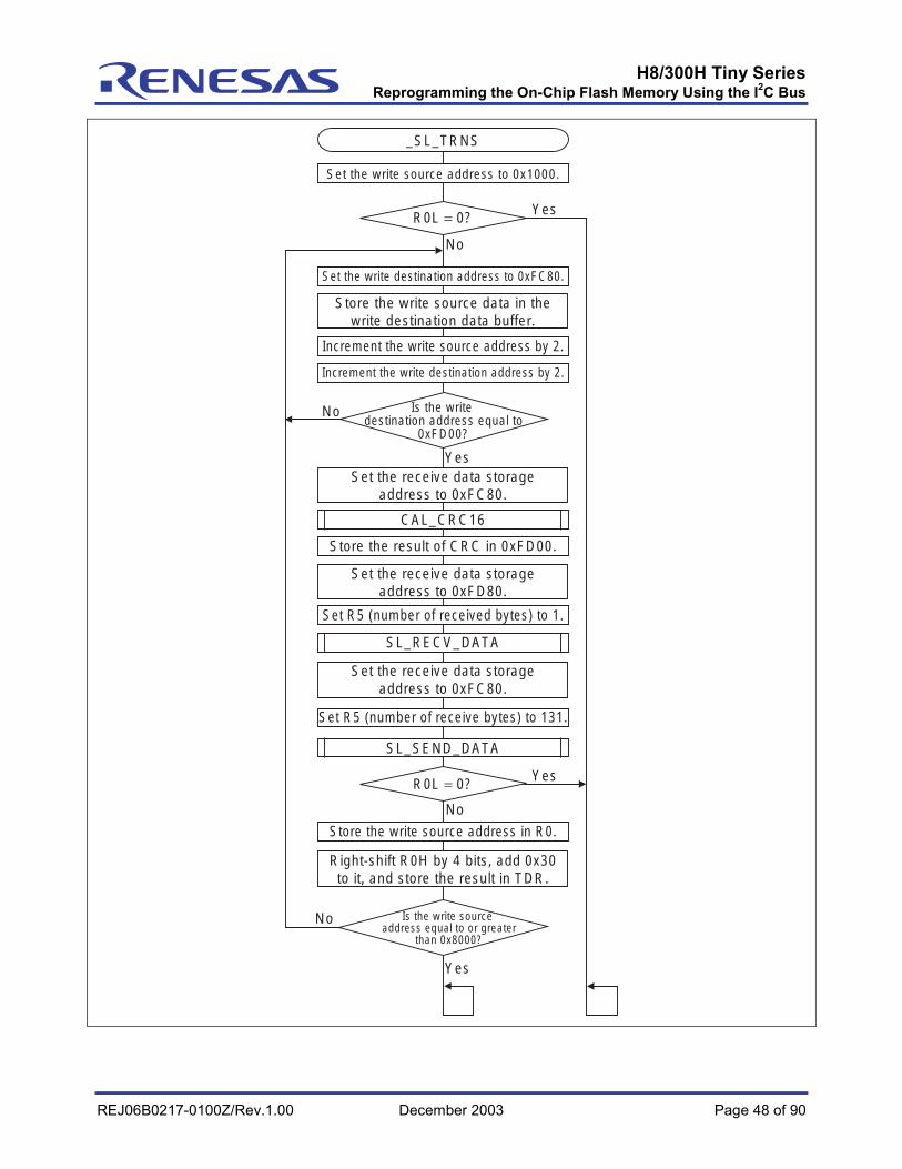
_SL_TRNS
Set the write source address to 0x1000.
Is the write destination address equal to
0xFD00?
No
Yes
Is the write source address equal to or greater
than 0x8000?
Store the result of CRC in 0xFD00.
Set R5 (number of received bytes) to 1.
Increment the write destination address by 2.
Increment the write source address by 2.
Store the write source data in the write destination data buffer.
Set the receive data storage address to 0xFC80.
Set the receive data storage address to 0xFD80.
Store the write source address in R0.
Right-shift R0H by 4 bits, add 0x30 to it, and store the result in TDR.
Yes
No
SL_SEND_DATA
R0L = 0?
Set R5 (number of receive bytes) to 131.
Set the receive data storage address to 0xFC80.
Set the write destination address to 0xFC80.
H8/300H Tiny SeriesReprogramming the On-Chip Flash Memory Using the I2C Bus
REJ06B0217-0100Z/Rev.1.00 December 2003 Page 49 of 90
Yes
No
No
Yes
No
Yes
Yes
No
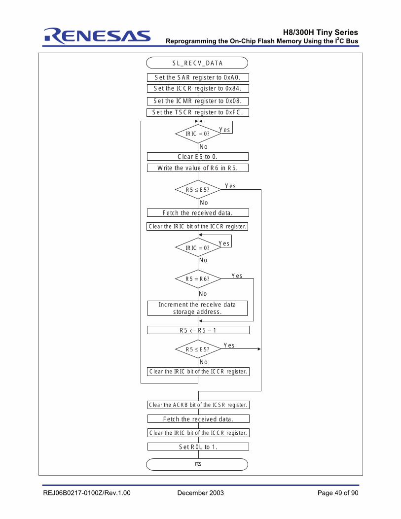
SL_RECV_DATA
Yes
No
IRIC = 0?
R5 ≤ E5?
R5 ≤ E5?
rts
IRIC = 0?
Set the ICCR register to 0x84.
Set the SAR register to 0xA0.
Set the ICMR register to 0x08.
Write the value of R6 in R5.
Clear E5 to 0.
Fetch the received data.
R5 = R6?
Clear the IRIC bit of the ICCR register.
Clear the IRIC bit of the ICCR register.
Clear the ACKB bit of the ICSR register.
Fetch the received data.
Set R0L to 1.
Clear the IRIC bit of the ICCR register.
R5 ← R5 − 1
Increment the receive data storage address.
Set the TSCR register to 0xFC.

H8/300H Tiny SeriesReprogramming the On-Chip Flash Memory Using the I2C Bus
REJ06B0217-0100Z/Rev.1.00 December 2003 Page 50 of 90
No
rts
Yes
No
Yes
No
1-1
Yes
No
Yes
No
1-1
Yes
No
Yes
SL_SEND_DATA
R0 = 100?
ACKB = 0?
ACKB = 0?
IRIC = 0?
AND the value of the ICCR register and 0xFE, OR the result and 0x04, and
store the result in the ICCR register.
OR the value of the ICCR register and 0x10 and store the result in the
ICCR register.
Clear the IRIC bit of the ICCR register.
Store the data to be sent in ICDR.
Clear the IRIC bit of the ICCR register.
Set E5 to 1.
Store the data to be sent in ICDR.
Increment the send data address.
Clear R0L to 0.
Clear R0 to 0.
Increment R0.
Set R0L to 1.
Set the ICDR register as R1L.
Clear the TRS bit of the ICCR register.
Clear the IRIC bit of the ICCR register.
R5 ≤ E5?
IRIC = 0?
E5 ← E5 + 1
AND the value of the ICCR register and 0xFA and store the result in the
ICCR register.
H8/300H Tiny SeriesReprogramming the On-Chip Flash Memory Using the I2C Bus
REJ06B0217-0100Z/Rev.1.00 December 2003 Page 51 of 90
Yes
No
Yes
No
Yes
No
rts
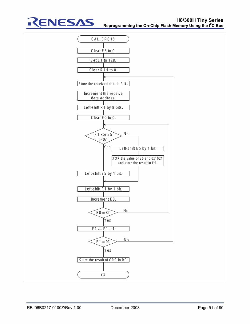
CAL_CRC16
E0 = 8?
E1 = 0?
Clear E5 to 0.
Set E1 to 128.
Clear R1H to 0.
Left-shift R1 by 8 bits.
Clear E0 to 0.
Left-shift E5 by 1 bit.
Left-shift R1 by 1 bit.
Increment E0.
Store the result of CRC in R0.
Left-shift E5 by 1 bit.
Increment the receive data address.
XOR the value of E5 and 0x1021 and store the result in E5.
Store the received data in R1L.
R1 xor E5 > 0?
E1 ← E1 − 1

H8/300H Tiny SeriesReprogramming the On-Chip Flash Memory Using the I2C Bus
REJ06B0217-0100Z/Rev.1.00 December 2003 Page 52 of 90
No
No
Yes
Yes
No
No
Yes
MA_SEND_DATA
_IIC_TEST
FL_ER_BLK
Yes
R0L = 0?
MA_RECV_DATA
2-3
2-1
2-2
CAL_CRC16
Store the value of the FENR register in R6 and set the FLSHE bit.
Set R0H to 0x10.
Set PDR1 to 0x06.
Set PCR1 to 0xFF.
Set the write start address to 0x1000.
Set the write end address to 0x8000.
Set MAXWT as the maximum number of writes.
Set R5 to 1.
Set R1 to 30.
Set R5 to 131.
Set the receive data storage address to 0xFC80.
Set the receive data storage address to 0xFC80.
Set the send data storage address to 0xFE14 and store the data to be sent in 0xA5.
No
Yes
No
R2 < R3?
FWRITE128
Set PDR1 to 0xE1.
R0L = 0?
Yes
NoR1 = R0? 2-2
2-4
Set the data at 0xFD00 in R1.
Increment the write start address by 128 and store the
address in R2.
Store the write end address in R3.
R0L = 0?
R1 = 0?
R0L = 0?
R1 ← R1 − 1
2-5
2-6
2-7
2-8
2-1
2-3
2-2
2-4
2-5
2-6
2-7
2-8
Set PDR1 to 0xE7.
Set PDR1 to 0xF4.
Set PDR1 to 0x71.
Set PDR1 to 0xF1.

H8/300H Tiny SeriesReprogramming the On-Chip Flash Memory Using the I2C Bus
REJ06B0217-0100Z/Rev.1.00 December 2003 Page 53 of 90
Yes
Yes
No
No
Yes
No
BLK1_ERASE
FR_ER_BLK
rts
R0L = 0?
rts
R0H= 0x08?
R0H= 0x10?
Set R1 to 0x0800.
Set R1 to 0x1000.
Set R2 to 0x8000.
Set R0L to 1.
Set R2 to 0x0C00.
Set R0H as the block to be erased.
Set R1 as the start address to be erased.
Set R2 as the end address to be erased.
Set the address of EBR1 (0xFF93) in R5.
Set the address of FLMCR1 (0xFF90) in R6.
Set MAXET as the maximum number of erases.

H8/300H Tiny SeriesReprogramming the On-Chip Flash Memory Using the I2C Bus
REJ06B0217-0100Z/Rev.1.00 December 2003 Page 54 of 90
No
Yes
rts rts
COUNT ← COUNT + 1
Yes
FL_WAIT FL_WAIT
No
BLK1_ERASE
FERASE
FL_WAIT
FERASEVF
R0L = 0?
FERASEVF
No
YesR0L = 0?
Set the SWE bit of the FLMCR register.
Set R0 to WLOOP1.
Clear COUNT.
COUNT < 100?
Clear the SWE bit of the FLMCR register.
Clear the SWE bit of the FLMCR register.
Set R0 to WLOOP100. Set R0 to WLOOP100.
Set R0L to 1. Clear R0L to 0.

H8/300H Tiny SeriesReprogramming the On-Chip Flash Memory Using the I2C Bus
REJ06B0217-0100Z/Rev.1.00 December 2003 Page 55 of 90
No
Yes
No
FL_WAIT
Yes
rtsrts
FL_WAIT
Set the verification start address as the address to
be verified.
FL_WAIT
FERASEVF
FL_WAIT
Set the EV bit of the FLMCR register.
Increment the verification start address.
Clear the EV bit of the FLMCR register.
Set R0 to WLOOP4.
Set R0L to 1. Clear R0L to 0.
Set R0 to WLOOP4.
Clear the EV bit of the FLMCR register.
Is verification data equal to
0xFFFF?
Is this the last address to be
verified?
Set R0 to WLOOP20.
Set R0 to WLOOP2.

H8/300H Tiny SeriesReprogramming the On-Chip Flash Memory Using the I2C Bus
REJ06B0217-0100Z/Rev.1.00 December 2003 Page 56 of 90
FERASE
Write 0x5A in the timer control/status register.
Write 0xF4 in the timer control/status register.
Set the EBR register bit corresponding to the bit number for
the block to be erased.
Set the count register to 100.
Yes
No
FL_WAIT
FL_WAIT
FL_WAIT
rts
R0 ← R0 − 1
R0 ≠ 0?
Set the ESU bit of the FLMCR register.
Clear the ESU bit of the FLMCR register.
Write 0x53 in the timer control/status register.
Clear the EBR register bit corresponding to the bit number
for the block to be erased.
Set R0 to WLOOP100.
Set R0 to TIME10000.
Set R0 to WLOOP10.
Set R0 to WLOOP10.
Clear the E bit of the FLMCR register.
Set the E bit of the FLMCR register.
Set φ/2048 as the input clock signal for the count register.

H8/300H Tiny SeriesReprogramming the On-Chip Flash Memory Using the I2C Bus
REJ06B0217-0100Z/Rev.1.00 December 2003 Page 57 of 90
Yes
No
FL_WAIT
rts
R0 ← R0 − 1
R0 ≠ 0?

H8/300H Tiny SeriesReprogramming the On-Chip Flash Memory Using the I2C Bus
REJ06B0217-0100Z/Rev.1.00 December 2003 Page 58 of 90
Yes
No
Yes
No
Yes
No
Yes
No
Yes
No
Yes
No
Yes
No
3-1
3-1
MA_SEND_DATA
rts
R5 ≤ E5?
ACKB = 0?
ACKB = 0?
BBSY = 0?
IRIC = 0?
IRIC = 0?
Set the ICCR register to 0x89.
Set the ICMR register to 0x08.
Set the TSCR register to 0xFC.
Set the ICDR register to 0xA0.
Clear the IRIC bit of the ICCR register.
Clear E5 to 0.
Store the data to be sent in ICDR.
Increment the send data address.
Set E5 to 1.
Clear R0L to 0. Set R0L to 1.
Clear the IRIC bit of the ICCR register.
OR the value of the ICCR register and 0x30 and store the result in the ICCR register.
AND the value of the ICCR register and 0xFE, OR the result and 0x04, and store the result in the ICCR register.
IRIC = 0?

H8/300H Tiny SeriesReprogramming the On-Chip Flash Memory Using the I2C Bus
REJ06B0217-0100Z/Rev.1.00 December 2003 Page 59 of 90
Yes
No
Yes
No
Yes
No
Yes
No
Yes
No
Yes
No
Yes
No
rts
R5 ≤ E5?
R5 = R6?
IRIC = 0?
IRIC = 0?
IRIC = 0?
IRIC = 0?
MA_RECV_DATA
Subtract 1 from R5.
Store the value of R5 in R6.
Clear the TRS bit of the ICCR register.
Set the WAIT bit of the ICMR register.
Fetch the received data.
Clear the IRIC bit of the ICCR register.
Clear the IRIC bit of the ICCR register.
Set E5 to 1.
Fetch the received data.Set the ACKB bit of the ICSR register.
Set the TRS bit of the ICCR register.
Clear the IRIC bit of the ICCR register.
Clear the WAIT bit of the ICMR register.
Fetch the received data.
Clear the IRIC bit of the ICCR register.
Set R0L to 1.
AND the value of the ICCR register and 0xFA and store the result in the
ICCR register.
Clear the IRIC bit of the ICCR register.
Increment the receive data address.
Clear the IRIC bit of the ICCR register.
Clear the ACKB bit of the ICSR register.
R5 ≤ E5?
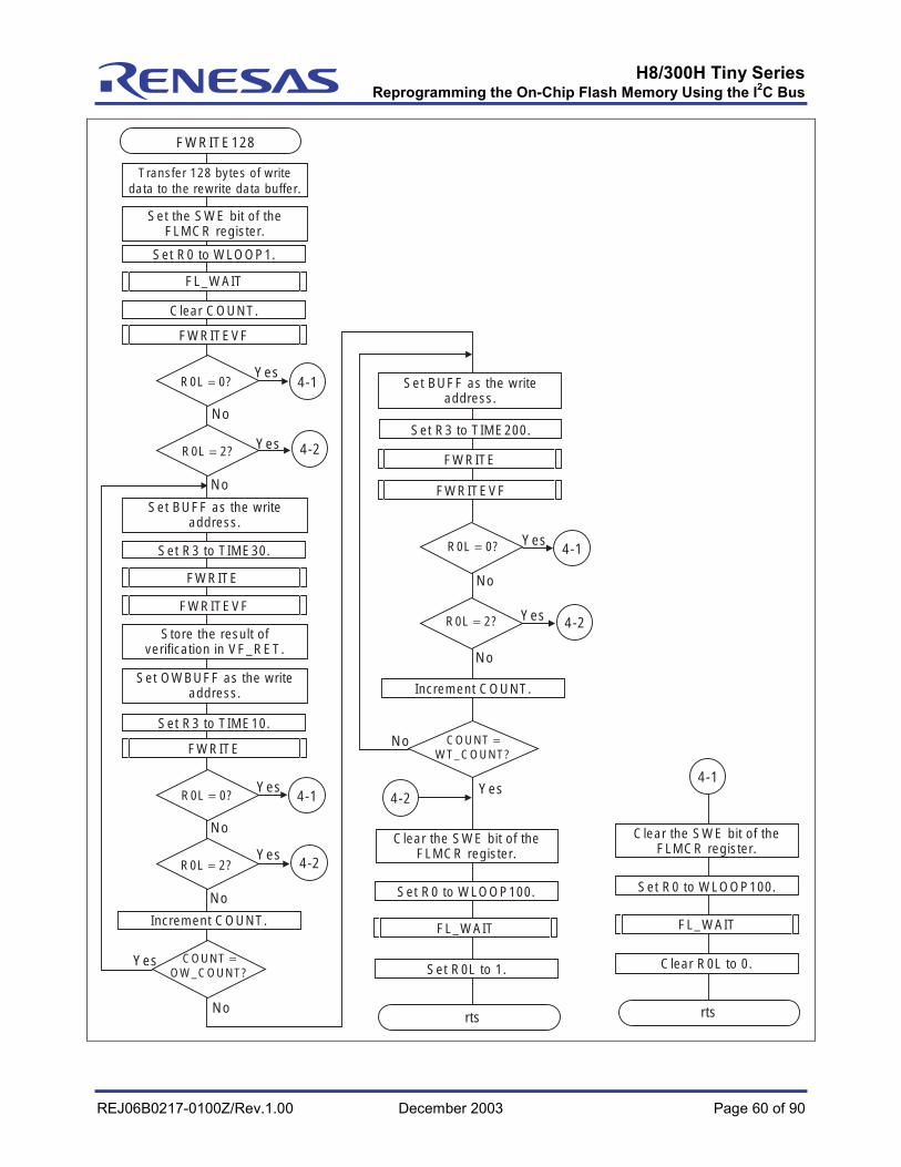
H8/300H Tiny SeriesReprogramming the On-Chip Flash Memory Using the I2C Bus
REJ06B0217-0100Z/Rev.1.00 December 2003 Page 60 of 90
No
Yes
No
Yes
Yes
No
No
Yes
No
Yes
No
Yes
No
Yes
Yes
No
4-2
4-1
4-2
4-24-1
4-2
4-1
4-1
FL_WAITFL_WAIT
FWRITEVF
FWRITE
FWRITEVF
FWRITE
FWRITE
FL_WAIT
FWRITEVF
rts rts
FWRITE128
R0L = 0?
R0L = 2?
R0L = 0?
R0L = 2?
R0L = 2?
R0L = 0?
Transfer 128 bytes of write data to the rewrite data buffer.
Set the SWE bit of the FLMCR register.
Set BUFF as the write address.
Set BUFF as the write address.
Store the result of verification in VF_RET.
Set OWBUFF as the write address.
Set R0 to WLOOP1.
Clear COUNT.
Set R3 to TIME200.
Increment COUNT.
Set R0 to WLOOP100. Set R0 to WLOOP100.
Set R0L to 1. Clear R0L to 0.
Set R3 to TIME30.
Set R3 to TIME10.
Increment COUNT.
COUNT = OW_COUNT?
COUNT = WT_COUNT?
Clear the SWE bit of the FLMCR register.
Clear the SWE bit of the FLMCR register.

H8/300H Tiny SeriesReprogramming the On-Chip Flash Memory Using the I2C Bus
REJ06B0217-0100Z/Rev.1.00 December 2003 Page 61 of 90
Yes
No
No
Yes
Yes
No
No
Yes
FL_WAIT
FL_WAIT
FL_WAIT
FL_WAIT
rtsrts
R0 ≠ 0?
E0 = 0xFFFF?
Set the PV bit of the FLMCR register.
FWRITEVF
Set BUFF as the rewrite address.
Set W_BUF as the write address.
Set R0 to WLOOP4.
Set R0 to WLOOP2.
Set R0 to WLOOP2.
Set the NG flag.
Set BUFF as the rewrite address.
Store rewrite data in E0.
Clear R0L to 0.
Clear the PV bit of the FLMCR register.
Clear the PV bit of the FLMCR register.
Set R0 to WLOOP2.
Set R0L to 2.
Set OWBUFF as the additional write address.
Write dummy data (0xFFFF) in flash memory. Is the write address
equal to W_BUF + 128?
Is the rewrite address equal to BUFF +
128?
Increment the flash memory write address.
Increment the rewrite data address.
Increment the flash memory write data address by 2.
OR flash memory data and rewrite data, and write the result in the additional write data buffer.
Increment the additional write address by 2.
Increment the rewrite address by 2.
OR flash memory data and write data, and store the result
in R0.
OR the inverse of flash memory data and write data, and write the result in the rewrite data buffer.

H8/300H Tiny SeriesReprogramming the On-Chip Flash Memory Using the I2C Bus
REJ06B0217-0100Z/Rev.1.00 December 2003 Page 62 of 90
Yes
No
Yes
No
FL_WAIT
FL_WAIT
FL_WAIT
rts
FWRITE
R3 ← R3 − 1
E0 ← E0 − 1
R0 ≠ 0?
E0 ≠ 0?
Set E0 to 128.
Write the data of the write source address to the write
destination address.
Increment the write source address.
Increment the write destination address.
Set the count register to 166.
Set R0 to WLOOP50.
Set the P bit of the FLMCR register.
Clear the P bit of the FLMCR register.
Set R0 to WLOOP5.
Set R0 to WLOOP5.
Write 0x5A in the timer control/status register.
Write 0xF4 in the timer control/status register.
Set the PSU bit of the FLMCR register.
Clear the PSU bit of the FLMCR register.
Write 0x53 in the timer control/status register.
Set φ/64 as the input clock signal for the count register.

H8/300H Tiny SeriesReprogramming the On-Chip Flash Memory Using the I2C Bus
REJ06B0217-0100Z/Rev.1.00 December 2003 Page 63 of 90
Trap instructions #1 to #4 Break condition interrupt Sleep instruction interrupt
IRQ #1 to #4 interrupt WKP interrupt
Overflow interrupt Timer (W, V) interrupt
IIC interrupt A/D conversion interrupt
Jump to INIT.
SCI3 interrupt
Jump to _Int_SCI3.
H8/300H Tiny SeriesReprogramming the On-Chip Flash Memory Using the I2C Bus
REJ06B0217-0100Z/Rev.1.00 December 2003 Page 64 of 90
9. Header File List
File: Fl_equ.h
;*********************************************************************
; FLASH ER/WR EQU 2001.07.09
;
;*********************************************************************
PDR1 .EQU H'FFD4 ; 7segLED Data
PCR1 .EQU H'FFE4 ; port direction
TDR .EQU H'FFAB ; SCI OUT
;*********************************************************************
; H8/3664F IIC REG
;*********************************************************************
ICCR .EQU H'FFC4 ;
ICSR .EQU H'FFC5 ;
ICDR .EQU H'FFC6 ;
ICMR .EQU H'FFC7 ;
SAR .EQU H'FFC7 ;
TSCR .EQU H'FFFC ;
;
TRS .BEQU 4,ICCR ;
ACKE .BEQU 3,ICCR ;
BBSY .BEQU 2,ICCR ;
IRIC .BEQU 1,ICCR ;
ACKB .BEQU 0,ICSR ;
WAIT .BEQU 6,ICMR ;
;
;*********************************************************************
;DEVICE_CODE .EQU H'A0 ;/* EEPROM DEVICE CODE:1010 */
DEVICE_CODE .EQU H'80 ;/* MPU DEVICE CODE:1000 */
SLAVE_ADRS .EQU H'00 ;/* SLAVE ADRS:0 */
IIC_DATA_W .EQU H'00 ;/* WRITE_DATA */
IIC_DATA_R .EQU H'01 ;/* READ_DATA */
;
;*********************************************************************
; H8/3664F FLASH REG
;*********************************************************************
FLMCR1 .EQU H'FF90 ; FLASH MEMORY CONTROL REGISTER 1
SWE: .EQU 6
ESU: .EQU 5
PSU: .EQU 4
EV: .EQU 3
PV: .EQU 2
E: .EQU 1
P: .EQU 0
FLMCR2 .EQU H'FF91 ; FLASH MEMORY CONTROL REGISTER 2
FLER: .EQU 7
EBR1 .EQU H'FF93 ; OBJECT BLOCK DESIGNATED REGISTER 1
FENR .EQU H'FF9B ; FLASH MEMORY ENABLE REGISTER
FLSHE: .EQU 7

H8/300H Tiny SeriesReprogramming the On-Chip Flash Memory Using the I2C Bus
REJ06B0217-0100Z/Rev.1.00 December 2003 Page 65 of 90
TCSRWD .EQU H'FFC0
TCWD .EQU H'FFC1
TMWD .EQU H'FFC2
;*********************************************************************
; WAIT TIME
;*********************************************************************
;
MHZ .EQU 11*100 ; 16MHZ
;
WLOOP1 .EQU 1*MHZ/400 ; ROOP WAIT TIME
WLOOP2 .EQU 2*MHZ/400
WLOOP4 .EQU 4*MHZ/400
WLOOP5 .EQU 5*MHZ/400
WLOOP6 .EQU 6*MHZ/400
WLOOP10 .EQU 10*MHZ/400
WLOOP20 .EQU 20*MHZ/400
WLOOP30 .EQU 30*MHZ/400
WLOOP50 .EQU 50*MHZ/400
WLOOP100 .EQU 100*MHZ/400
TIME10 .EQU 10*MHZ/400 ; WRITE WAIT TIME
TIME30 .EQU 30*MHZ/400 ; WRITE WAIT TIME
TIME200 .EQU 200*MHZ/400 ; WRITE WAIT TIME
TIME10000 .EQU 10000*MHZ/400 ; ERASE WAIT TIME
;*********************************************************************
; Constants
;*********************************************************************
MAXWT .EQU 1000 ; MAX WRITE COUNT
MAXET .EQU 100 ; MAX ERASE COUNT
OW_COUNT .EQU 6 ; OVER WRITE COUNT
OK .EQU H'0 ; OK FLAG
NG .EQU H'1 ; ERR FLAG
WNG .EQU H'2 ; WRITE ERR
File: lic_ram.h
; 2001.07.05
;//RAM area for the H8S/3664F erase/write program//
;
W_BUF .EQU H'FC80 ;.B128 WRITE DATA AREA
BUFF .EQU H'FD00 ;.B128 RETRY WRITE DATA AREA
OWBUFF .EQU H'FD80 ;.B128 OVER WRITE DATA ARIA
COUNT .EQU H'FE00 ;.W1 W_COUNT,E_COUNT
W_ADR .EQU H'FE02 ;.W1 WRITE ADDRESS AREA
W_ADR_ED .EQU H'FE04 ;.W1 WRITE ADDRESS AREA
ET_COUNT .EQU H'FE08 ;.W1 MAX E_COUNT
WT_COUNT .EQU H'FE0A ;.W1 MAX W_COUNT
EVF_ST .EQU H'FE0C ;.W1 ERASE VERIFY START ADDRESS
EVF_ED .EQU H'FE0E ;.W1 ERASE VERIFY END ADDRESS
BLK_NO .EQU H'FE10 ;.B1 ERASE BIT NUMBER
VF_RET .EQU H'FE11 ;.B1 VERIFY CHECK
IIC_SBUF .EQU H'FE14 ;.B12 IIC SEND BUF

H8/300H Tiny SeriesReprogramming the On-Chip Flash Memory Using the I2C Bus
REJ06B0217-0100Z/Rev.1.00 December 2003 Page 66 of 90
10. Program Listing
File: INIT.SRC
.EXPORT _INIT
.EXPORT _jump_prog
.IMPORT _main
;
.SECTION PM,CODE
_INIT:
MOV.W #H'FF80,R7
LDC.B #B'10000000,CCR
JMP @_main
;
;/* Assembler routine */
;
_jump_prog:
JSR @R0
;
.END
File: FLWR.c
/************************************************************************/
/* */
/* FILE :FLWR.c */
/* DATE :Thr, Aug 09, 2001 */
/* DESCRIPTION :Main Program */
/* CPU TYPE :H8/3664F */
/* */
/* This file is generated by Renesas Project Generator (Ver.1.2). */
/* */
/************************************************************************/
#include "machine.h"
#define PDR5 *(volatile unsigned char *)0xFFD8
#define PMR5 *(volatile unsigned char *)0xFFE1
#define PCR5 *(volatile unsigned char *)0xFFE8
#define PDR8 *(volatile unsigned char *)0xFFDB
#define PCR8 *(volatile unsigned char *)0xFFEB
#define PCR1 *(volatile unsigned char *)0xFFE4 /* 7segLED Data */
#define PDR1 *(volatile unsigned char *)0xFFD4 /* 7segLED Data */
/*;********************************************************/
/*; Function Definitions */
/*;********************************************************/
extern void INIT(void);
extern void jump_prog( unsigned short );
extern void SL_TRNS ( void );
extern void u_main ( void );
H8/300H Tiny SeriesReprogramming the On-Chip Flash Memory Using the I2C Bus
REJ06B0217-0100Z/Rev.1.00 December 2003 Page 67 of 90
void flprg_cpy ( void );
void main ( void );
void wait ( unsigned int limit );
#ifdef __cplusplus
extern "C"
#endif
void abort(void);
#ifdef __cplusplus
#endif
#pragma section M /* P */
/*;**********************************************************/
/*; Main Program */
/*;**********************************************************/
void main(void)
int i;
unsigned char sw_d1,sw_d2;
PCR5 = 0x00; /* Port 5 input */
PCR1 = 0x00; /* Port 1 input */
PDR8 = 0x00; /* Port 84 low */
PCR8 = 0x10; /* Port 84 output */
i = 0;
while (i < 500) /* Wait for 5 seconds. */
PDR8 = 0x00;
wait(10000);
PDR8 = 0x10;
wait(10000);
sw_d1 = ((PDR5 & 0x20) | (PDR1 & 0x10));
sw_d2 = ((PDR5 & 0x20) | (PDR1 & 0x10));
if (sw_d1 == sw_d2)
if (sw_d1 == 0x10)
SL_TRNS(); /* IIC trns */
if (sw_d1 == 0x20)
flprg_cpy();
jump_prog( 0xf780 ); /* IIC recv & FLASH_WR */
i++;
u_main();
/*;**********************************************************/
/*; Program Copy ( ROM:0400-08FF -> RAM:F780-FB7F ) */
/*;**********************************************************/
void flprg_cpy( void )
unsigned short *ptr,*r_ptr;
H8/300H Tiny SeriesReprogramming the On-Chip Flash Memory Using the I2C Bus
REJ06B0217-0100Z/Rev.1.00 December 2003 Page 68 of 90
ptr=(unsigned short*)0x0400;
r_ptr=(unsigned short*)0xf780;
while(ptr < (unsigned short*)0x900)
*r_ptr++ = *ptr++;
void wait( unsigned int limit)
unsigned int cnt;
cnt = 0;
while (cnt < limit)
cnt++;
void abort(void)
File: IIC_SL.src
;*********************************************************************
; IIC_SL_SUB Ver1.0 2001.07.16
;
;*********************************************************************
.INCLUDE "IIC_RAM.H"
.INCLUDE "FL_EQU.H" ; FLASH ER/WR EQU
;
.IMPORT CAL_CRC16
.EXPORT SL_TRNS
;
.SECTION PF_2
.DISPSIZE FBR=16
;
;*********************************************************************
; SL_TRNS
;*********************************************************************
_SL_TRNS:
MOV.W #H'1000,R3 ; ptr = 0x1000
;
MOV.B #DEVICE_CODE|SLAVE_ADRS,R1L
MOV.B R1L,@SAR
;
MOV.B #H'FC,R1L
MOV.B R1L,@TSCR
;
SL_TRNS10
MOV.W #W_BUF,R1
SL_TRNS20
MOV.W @R3,R0 ; *ptr
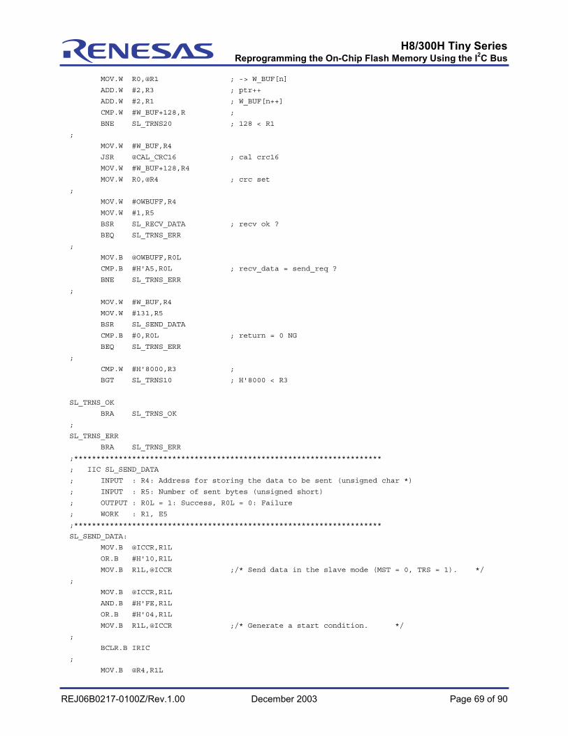
H8/300H Tiny SeriesReprogramming the On-Chip Flash Memory Using the I2C Bus
REJ06B0217-0100Z/Rev.1.00 December 2003 Page 69 of 90
MOV.W R0,@R1 ; -> W_BUF[n]
ADD.W #2,R3 ; ptr++
ADD.W #2,R1 ; W_BUF[n++]
CMP.W #W_BUF+128,R ;
BNE SL_TRNS20 ; 128 < R1
;
MOV.W #W_BUF,R4
JSR @CAL_CRC16 ; cal crc16
MOV.W #W_BUF+128,R4
MOV.W R0,@R4 ; crc set
;
MOV.W #OWBUFF,R4
MOV.W #1,R5
BSR SL_RECV_DATA ; recv ok ?
BEQ SL_TRNS_ERR
;
MOV.B @OWBUFF,R0L
CMP.B #H'A5,R0L ; recv_data = send_req ?
BNE SL_TRNS_ERR
;
MOV.W #W_BUF,R4
MOV.W #131,R5
BSR SL_SEND_DATA
CMP.B #0,R0L ; return = 0 NG
BEQ SL_TRNS_ERR
;
CMP.W #H'8000,R3 ;
BGT SL_TRNS10 ; H'8000 < R3
SL_TRNS_OK
BRA SL_TRNS_OK
;
SL_TRNS_ERR
BRA SL_TRNS_ERR
;*********************************************************************
; IIC SL_SEND_DATA
; INPUT : R4: Address for storing the data to be sent (unsigned char *)
; INPUT : R5: Number of sent bytes (unsigned short)
; OUTPUT : R0L = 1: Success, R0L = 0: Failure
; WORK : R1, E5
;*********************************************************************
SL_SEND_DATA:
MOV.B @ICCR,R1L
OR.B #H'10,R1L
MOV.B R1L,@ICCR ;/* Send data in the slave mode (MST = 0, TRS = 1). */
;
MOV.B @ICCR,R1L
AND.B #H'FE,R1L
OR.B #H'04,R1L
MOV.B R1L,@ICCR ;/* Generate a start condition. */
;
BCLR.B IRIC
;
MOV.B @R4,R1L

H8/300H Tiny SeriesReprogramming the On-Chip Flash Memory Using the I2C Bus
REJ06B0217-0100Z/Rev.1.00 December 2003 Page 70 of 90
MOV.B R1L,@ICDR ;/* Set transmission data. */
;
BCLR.B IRIC
SL_SEND_D30
BTST.B IRIC ;/* Is transmission completed? */
BEQ SL_SEND_D30
;
BTST.B ACKB
BNE SL_SEND_NG ;/* Is an ACK sent? */
;
MOV.W #1,E5 ; cnt = 1;
SL_SEND_D40
CMP.W R5,E5 ; no <= cnt
BCC SL_SEND_D60 ; R5 <= E5 (C=1)
; ; no > cnt
MOV.B @R4,R1L ;ICDR = *ptr /* Set n data items. */
MOV.B R1L,@ICDR ;
BCLR.B IRIC
ADD.W #1,R4 ;ptr++
SL_SEND_D50
BTST.B IRIC ;/* Are n data items sent? */
BEQ SL_SEND_D50
;
BTST.B ACKB
BNE SL_SEND_NG ;/* Is an ACK sent? */
;
ADD.W #1,E5 ; cnt++
BRA SL_SEND_D40
;
SL_SEND_D60
MOV.W #0,R0 ; dummy wait
SL_SEND_D70 ;
ADD.W #1,R0 ;
CMP.W #40,R0 ;
BNE SL_SEND_D70 ;
;
MOV.B #1,R0L ; return(1)
SL_SEND_D90
BCLR TRS ; ICCR.TRS = 0;
MOV.B @ICDR,R1L ; dummy = ICDR;
;
MOV.B @ICCR,R1L ;
AND.B #H'FA,R1L ;
MOV.B R1L,@ICCR ; ICCR &= 0xfa;
;
RTS
;
SL_SEND_NG
MOV.B #0,R0L ; return(0)
BRA SL_SEND_D90
;*********************************************************************
; IIC SL_RECV_DATA
; INPUT : R4: Address for storing the received data (unsigned char *)
; INPUT : R5: Number of received bytes (unsigned short)

H8/300H Tiny SeriesReprogramming the On-Chip Flash Memory Using the I2C Bus
REJ06B0217-0100Z/Rev.1.00 December 2003 Page 71 of 90
; OUTPUT : R0L = 1: Success
; WORK : R1, E5, R6
;*********************************************************************
SL_RECV_DATA:
MOV.B #H'84,R1L ;/* ICE=1(P57,P56->SCL,SDA), */
MOV.B R1L,@ICCR
MOV.B #H'08,R1L
MOV.B R1L,@ICMR
;
BCLR.B ACKB
;
SL_RECV_D10
BTST.B IRIC ;/* Is reception completed? */
BEQ SL_RECV_D10
;
MOV.W #0,E5
SL_RECV_D20
CMP.W R5,E5 ; no < 0
BCC SL_RECV_D60 ; R5 <= E5 (C=1)
; ; no > 1
MOV.B @ICDR,R1L
MOV.B R1L,@R4 ;/* Fetch received data. */
BCLR.B IRIC
SL_RECV_D40
BTST.B IRIC ;/* Is reception completed? */
BEQ SL_RECV_D40
;
MOV.B @R4,R1L
CMP.B #DEVICE_CODE|SLAVE_ADRS,R1L
BEQ SL_RECV_D50
;
ADD.W #1,R4 ; ptr++
SL_RECV_D50
SUB.W #1,R5
CMP.W R5,E5 ; no <= 1
BCC SL_RECV_D60 ; R5 <= E5 (C=1)
;
BCLR.B IRIC
;
BRA SL_RECV_D20
;
SL_RECV_D60
BCLR.B ACKB
MOV.B @ICDR,R1L
MOV.B R1L,@R4 ;/* Fetch received data. */
BCLR.B IRIC
;
MOV.B #1,R0L
RTS
;*********************************************************************
.END

H8/300H Tiny SeriesReprogramming the On-Chip Flash Memory Using the I2C Bus
REJ06B0217-0100Z/Rev.1.00 December 2003 Page 72 of 90
File: IIC_MA.src
;*********************************************************************
; IIC_MA_SUB Ver1.0 2001.07.05
;
;*********************************************************************
.INCLUDE "IIC_RAM.H"
.INCLUDE "FL_EQU.H" ; FLASH ER/WR EQU
;
.EXPORT _IIC_TEST
.EXPORT CAL_CRC16
;*********************************************************************
; IIC TEST 2001.07.05
;
;*********************************************************************
.SECTION PF_1
.DISPSIZE FBR=16
;*********************************************************************
_IIC_TEST:
;=============Turn on flash memory enable register.==================
MOV.W #FENR,R6
BSET.B #FLSHE,@R6 ; Set the FLSHE bit.
;====================================================================
;============Turn on flash memory control register 1.================
; MOV.W #FLMCR1,R0
; BSET.B #SWE,@R0 ; Set the SWE bit.
;====================================================================
;
MOV.B #H'10,R0H ; EB4 set
BSR FL_ER_BLK ; BLOCK ERASE
CMP.B #OK,R0L ;
BNE FL_ER_ERR
;
MOV.W #H'1000,R0
MOV.W R0,@W_ADR ; Write beginning address
MOV.W #H'8000,R0
MOV.W R0,@W_ADR_ED ; Write ending address
MOV.W #MAXWT,R0 ; Set the maximum number of writes.
MOV.W R0,@WT_COUNT
;
; MOV.W #10,R3 ; loop cnt
IIC_TEST00
;
FL_TEST20
MOV.W #IIC_SBUF,R4 ; input:R4(buf_adrs)
MOV.B #H'A5,R1L ;
MOV.B R1L,@R4 ; IIC_BUF[0]=H'A5
MOV.W #1,R5 ; input:R5(cnt)
BSR MA_SEND_DATA ; /* Send */
BEQ IIC_SEND_ERR
;
MOV.W #30,R1
IIC_TEST10

H8/300H Tiny SeriesReprogramming the On-Chip Flash Memory Using the I2C Bus
REJ06B0217-0100Z/Rev.1.00 December 2003 Page 73 of 90
SUB.W #1,R1
BNE IIC_TEST10 ; wait
;
MOV.W #W_BUF,R4 ; input:R4(buf_adrs)
MOV.W #131,R5 ; input:R5(cnt)
BSR MA_RECV_DATA ; /* Receive */
BEQ IIC_RECV_ERR
;
MOV.W #W_BUF,R4 ; input:R4(buf_adrs)
BSR CAL_CRC16 ;
MOV.W #W_BUF+128,R4 ; input:R4(crc_adrs)
MOV.W @R4,R1
CMP.W R1,R0
BNE IIC_RECV_ERR
;
BSR FWRITE128 ; Write flash memory (in units of 128 bytes).
CMP.B #OK,R0L
BNE FL_WR_ERR
;
MOV.W @W_ADR_ED,R3 ; Write ending address
MOV.W @W_ADR,R2 ; Write beginning address
ADD.W #128,R2 ; Increment the address by 128.
MOV.W R2,@W_ADR ;
CMP.W R2,R3 ;
BHI FL_TEST20 ; R3(END) > R2 (unsigned)
;
;*********************************************************************
; IIC_TEST END
;*********************************************************************
;
IIC_TEST_OK
IIC_SEND_ERR
IIC_RECV_ERR
FL_ER_ERR
FL_WR_ERR
;==============Turn off flash memory enable register.=================
MOV.W #FENR,R6
BCLR.B #FLSHE,@R6 ; Set the FLSHE bit.
;=====================================================================
ERR_LOOP
BRA ERR_LOOP
;*********************************************************************
; IIC MA_SEND_DATA
; INPUT : R4: Address for storing the data to be sent (unsigned char *)
; INPUT : R5: Number of sent bytes (unsigned short)
; OUTPUT : R0L = 1: Success, R0L = 0: Failure
; WORK : R1, E5
;*********************************************************************
MA_SEND_DATA:
MOV.B #H'89,R1L ;/* ICE=1(P57,P56->SCL,SDA), */
MOV.B R1L,@ICCR
MOV.B #H'08,R1L
MOV.B R1L,@ICMR
MOV.B #H'FC,R1L

H8/300H Tiny SeriesReprogramming the On-Chip Flash Memory Using the I2C Bus
REJ06B0217-0100Z/Rev.1.00 December 2003 Page 74 of 90
MOV.B R1L,@TSCR
MA_SEND_D10
BTST.B BBSY ;/* Is the bus busy? */
BNE MA_SEND_D10
;
MOV.B @ICCR,R1L
OR.B #H'30,R1L
MOV.B R1L,@ICCR ;/* Send data in the master mode (MST = 1, TRS = 1). */
;
MOV.B @ICCR,R1L
AND.B #H'FE,R1L
OR.B #H'04,R1L
MOV.B R1L,@ICCR ;/* Generate a start condition. */
MA_SEND_D20
BTST.B IRIC ;/* Is transmission successful? */
BEQ MA_SEND_D20
;
MOV.B #DEVICE_CODE|SLAVE_ADRS|IIC_DATA_W,R1L
MOV.B R1L,@ICDR ;/* Set the start slave address. */
;
BCLR.B IRIC
MA_SEND_D30
BTST.B IRIC ;/* Is transmission completed? */
BEQ MA_SEND_D30
;
BTST.B ACKB
BNE MA_SEND_NG ;/* Is an ACK sent? */
;
MOV.W #0,E5 ; cnt = 0;
MA_SEND_D40
CMP.W R5,E5 ; no <= cnt
BCC MA_SEND_D60 ; R5 <= E5 (C=1)
; ; no > cnt
MOV.B @R4,R1L ;ICDR = *ptr /* Set n data items. */
MOV.B R1L,@ICDR ;
BCLR.B IRIC
ADD.W #1,R4 ;ptr++
MA_SEND_D50
BTST.B IRIC ;/* Are n data items sent? */
BEQ MA_SEND_D50
;
BTST.B ACKB
BNE MA_SEND_NG ;/* Is an ACK sent? */
;
ADD.W #1,E5 ; cnt++
BRA MA_SEND_D40
;
MA_SEND_D60
MOV.B #1,R0L ; return(1)
MA_SEND_D90
RTS
MA_SEND_NG
MOV.B #0,R0L ; return(0)
BRA MA_SEND_D90

H8/300H Tiny SeriesReprogramming the On-Chip Flash Memory Using the I2C Bus
REJ06B0217-0100Z/Rev.1.00 December 2003 Page 75 of 90
;*********************************************************************
; IIC MA_RECV_DATA
; INPUT : R4: Address for storing the received data (unsigned char *)
; INPUT : R5: Number of received bytes (unsigned short)
; OUTPUT : R0L = 1: Success
; WORK : R1, E5, R6
;*********************************************************************
MA_RECV_DATA:
MOV.W R5,R6
;
BCLR.B TRS ;/* Receive data in the master mode. */
BSET.B WAIT
BCLR.B ACKB
;
MOV.B @ICDR,R1L ;/* Read dummy data. */
MOV.B R1L,@R4 ;/* Fetch the received data. */
;
BCLR.B IRIC
MA_RECV_D10
BTST.B IRIC ;/* Is reception completed? */
BEQ MA_RECV_D10
;
BCLR.B IRIC
MA_RECV_D20
MOV.W #1,E5
CMP.W R5,E5 ; no <= 1
BCC MA_RECV_D60 ; R5 <= E5 (C=1)
; ; no > 1
MA_RECV_D30
BTST.B IRIC ;/* Is reception completed? */
BEQ MA_RECV_D30
;
MOV.B @ICDR,R1L
MOV.B R1L,@R4 ;/* Fetch the received data. */
BCLR.B IRIC
MA_RECV_D40
BTST.B IRIC ;/* Is reception completed? */
BEQ MA_RECV_D40
;
CMP.W R5,R6 ;
BEQ MA_RECV_D50
;
ADD.W #1,R4 ; ptr++
MA_RECV_D50
SUB.W #1,R5
CMP.W R5,E5 ; no <= 1
BCC MA_RECV_D60 ; R5 <= E5 (C=1)
;
BCLR.B IRIC
;
BRA MA_RECV_D20
;
MA_RECV_D60

H8/300H Tiny SeriesReprogramming the On-Chip Flash Memory Using the I2C Bus
REJ06B0217-0100Z/Rev.1.00 December 2003 Page 76 of 90
BSET.B ACKB
BSET.B TRS
BCLR.B IRIC
MA_RECV_D70
BTST.B IRIC ;/* Is reception completed? */
BEQ MA_RECV_D70
;
BCLR.B WAIT
MOV.B @ICDR,R1L
MOV.B R1L,@R4 ;/* Fetch the received data. */
BCLR.B IRIC
;
MOV.B @ICCR,R1L ;
AND.B #H'FA,R1L ;
MOV.B R1L,@ICCR ; ICCR & 0xfa
;
MOV.B #1,R0L
RTS
;*********************************************************************
; CAL_CRC16
; INPUT : R4: Address for storing the received data (unsigned char *)
; WORK : E0(k),R0(0x1021),E1(cnt),R1(data),R2(work),E5(crc)
;*********************************************************************
CAL_CRC16:
MOV.W #H'1021,R0
MOV.W #0,E5 ; crc = 0;
MOV.W #128,E1 ; cnt = 128
MOV.B #0,R1H
CAL_CRC10
MOV.B @R4,R1L ; data = *ptr
ADD.W #1,R4 ; ptr++
SHLL.W R1 ; data << 1 (1)
SHLL.W R1 ; data << 1 (2)
SHLL.W R1 ; data << 1 (3)
SHLL.W R1 ; data << 1 (4)
SHLL.W R1 ; data << 1 (5)
SHLL.W R1 ; data << 1 (6)
SHLL.W R1 ; data << 1 (7)
SHLL.W R1 ; data << 1 (8)
;
MOV.W #0,E0 ; k= 0;
CAL_CRC20
MOV.W R1,R2
XOR.W E5,R2 ; crc ^ data
BPL CAL_CRC30
SHLL.W E5 ; crc << 1
XOR.W R0,E5 ; 0x1021 ^ crc
BRA CAL_CRC40
CAL_CRC30
SHLL.W E5 ; crc << 1
CAL_CRC40
SHLL.W R1 ; data >> 1
ADD.W #1,E0 ; k++
CMP.W #8,E0
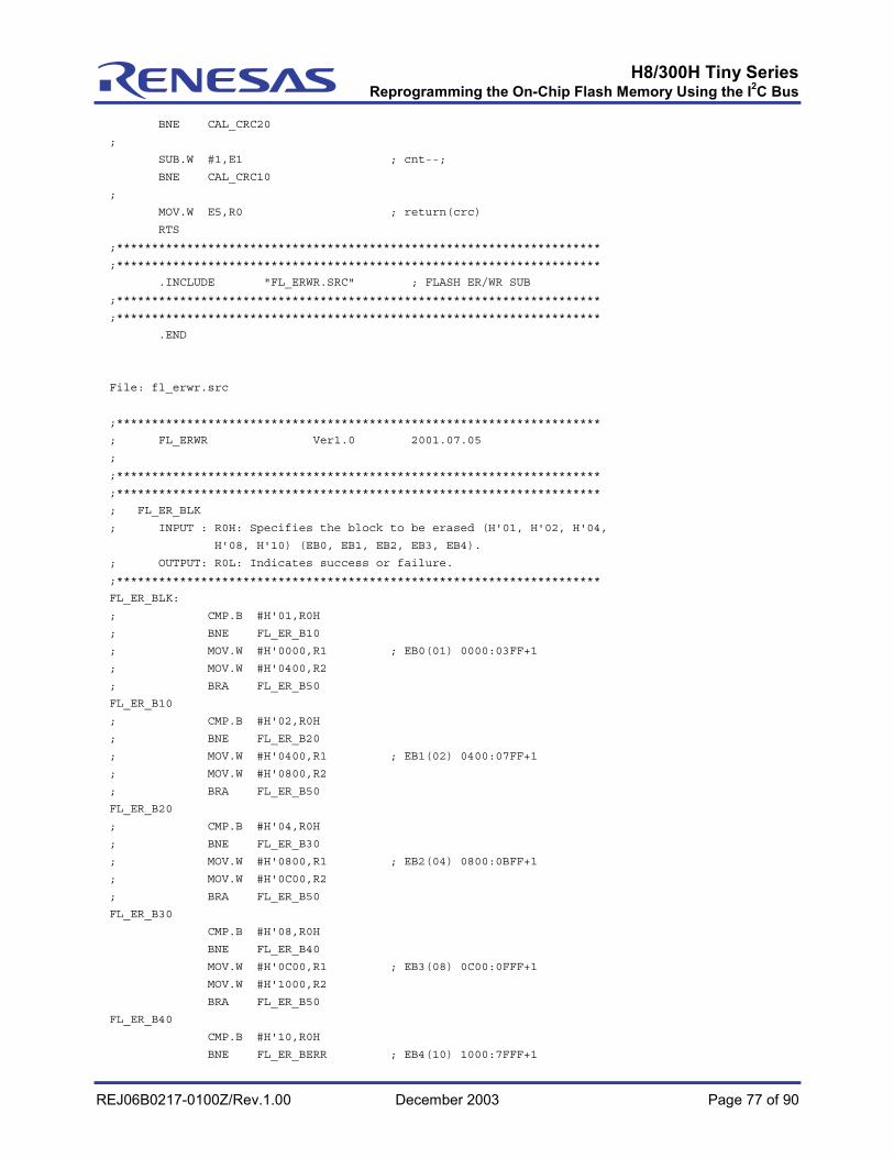
H8/300H Tiny SeriesReprogramming the On-Chip Flash Memory Using the I2C Bus
REJ06B0217-0100Z/Rev.1.00 December 2003 Page 77 of 90
BNE CAL_CRC20
;
SUB.W #1,E1 ; cnt--;
BNE CAL_CRC10
;
MOV.W E5,R0 ; return(crc)
RTS
;*********************************************************************
;*********************************************************************
.INCLUDE "FL_ERWR.SRC" ; FLASH ER/WR SUB
;*********************************************************************
;*********************************************************************
.END
File: fl_erwr.src
;*********************************************************************
; FL_ERWR Ver1.0 2001.07.05
;
;*********************************************************************
;*********************************************************************
; FL_ER_BLK
; INPUT : R0H: Specifies the block to be erased (H'01, H'02, H'04,
H'08, H'10) (EB0, EB1, EB2, EB3, EB4).
; OUTPUT: R0L: Indicates success or failure.
;*********************************************************************
FL_ER_BLK:
; CMP.B #H'01,R0H
; BNE FL_ER_B10
; MOV.W #H'0000,R1 ; EB0(01) 0000:03FF+1
; MOV.W #H'0400,R2
; BRA FL_ER_B50
FL_ER_B10
; CMP.B #H'02,R0H
; BNE FL_ER_B20
; MOV.W #H'0400,R1 ; EB1(02) 0400:07FF+1
; MOV.W #H'0800,R2
; BRA FL_ER_B50
FL_ER_B20
; CMP.B #H'04,R0H
; BNE FL_ER_B30
; MOV.W #H'0800,R1 ; EB2(04) 0800:0BFF+1
; MOV.W #H'0C00,R2
; BRA FL_ER_B50
FL_ER_B30
CMP.B #H'08,R0H
BNE FL_ER_B40
MOV.W #H'0C00,R1 ; EB3(08) 0C00:0FFF+1
MOV.W #H'1000,R2
BRA FL_ER_B50
FL_ER_B40
CMP.B #H'10,R0H
BNE FL_ER_BERR ; EB4(10) 1000:7FFF+1
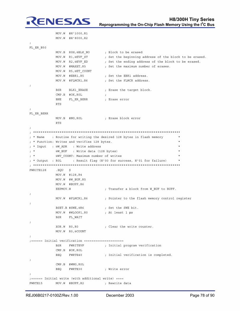
H8/300H Tiny SeriesReprogramming the On-Chip Flash Memory Using the I2C Bus
REJ06B0217-0100Z/Rev.1.00 December 2003 Page 78 of 90
MOV.W #H'1000,R1
MOV.W #H'8000,R2
;
FL_ER_B50
MOV.B R0H,@BLK_NO ; Block to be erased
MOV.W R1,@EVF_ST ; Set the beginning address of the block to be erased.
MOV.W R2,@EVF_ED ; Set the ending address of the block to be erased.
MOV.W #MAXET,R5 ; Set the maximum number of erases.
MOV.W R5,@ET_COUNT
MOV.W #EBR1,R5 ; Set the EBR1 address.
MOV.W #FLMCR1,R6 ; Set the FLMCR address.
;
BSR BLK1_ERASE ; Erase the target block.
CMP.B #OK,R0L ;
BNE FL_ER_BERR ; Erase error
RTS
;
FL_ER_BERR
MOV.B #NG,R0L ; Erase block error
RTS
;
; ******************************************************************************
; * Name : Routine for writing the desired 128 bytes in flash memory *
; * Function: Writes and verifies 128 bytes. *
; * Input : @W_ADR : Write address *
; * @W_BUF : Write data (128 bytes) *
; * @WT_COUNT: Maximum number of writes *
; * Output : R0L : Result flag (H'00 for success, H'01 for failure) *
; ******************************************************************************
FWRITE128 .EQU $
MOV.W #128,R4
MOV.W #W_BUF,R5
MOV.W #BUFF,R6
EEPMOV.W ; Transfer a block from W_BUF to BUFF.
;
MOV.W #FLMCR1,R6 ; Pointer to the flash memory control register
;
BSET.B #SWE,@R6 ; Set the SWE bit.
MOV.W #WLOOP1,R0 ; At least 1 µs BSR FL_WAIT
;
XOR.W R0,R0 ; Clear the write counter.
MOV.W R0,@COUNT
;
;====== Initial verification =====================
BSR FWRITEVF ; Initial program verification
CMP.B #OK,R0L
BEQ FWRTE40 ; Initial verification is completed.
;
CMP.B #WNG,R0L
BEQ FWRTE30 ; Write error
;
;====== Initial write (with additional write) ====
FWRTE15 MOV.W #BUFF,R2 ; Rewrite data
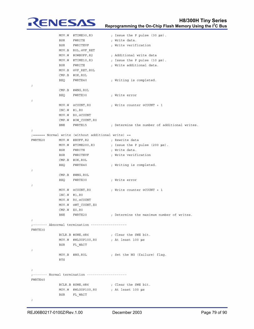
H8/300H Tiny SeriesReprogramming the On-Chip Flash Memory Using the I2C Bus
REJ06B0217-0100Z/Rev.1.00 December 2003 Page 79 of 90
MOV.W #TIME30,R3 ; Issue the P pulse (30 µs). BSR FWRITE ; Write data.
BSR FWRITEVF ; Write verification
MOV.B R0L,@VF_RET
MOV.W #OWBUFF,R2 ; Additional write data
MOV.W #TIME10,R3 ; Issue the P pulse (10 µs). BSR FWRITE ; Write additional data.
MOV.B @VF_RET,R0L
CMP.B #OK,R0L
BEQ FWRTE40 ; Writing is completed.
;
CMP.B #WNG,R0L
BEQ FWRTE30 ; Write error
;
MOV.W @COUNT,R0 ; Write counter @COUNT + 1
INC.W #1,R0
MOV.W R0,@COUNT
CMP.W #OW_COUNT,R0
BNE FWRTE15 ; Determine the number of additional writes.
;
;====== Normal write (without additional write) ==
FWRTE20 MOV.W #BUFF,R2 ; Rewrite data
MOV.W #TIME200,R3 ; Issue the P pulse (200 µs). BSR FWRITE ; Write data.
BSR FWRITEVF ; Write verification
CMP.B #OK,R0L
BEQ FWRTE40 ; Writing is completed.
;
CMP.B #WNG,R0L
BEQ FWRTE30 ; Write error
;
MOV.W @COUNT,R0 ; Write counter @COUNT + 1
INC.W #1,R0
MOV.W R0,@COUNT
MOV.W @WT_COUNT,E0
CMP.W E0,R0
BNE FWRTE20 ; Determine the maximum number of writes.
;
;------- Abnormal termination ------------------
FWRTE30
BCLR.B #SWE,@R6 ; Clear the SWE bit.
MOV.W #WLOOP100,R0 ; At least 100 µs BSR FL_WAIT
;
MOV.B #NG,R0L ; Set the NG (failure) flag.
RTS
;
;------- Normal termination --------------------
FWRTE40
BCLR.B #SWE,@R6 ; Clear the SWE bit.
MOV.W #WLOOP100,R0 ; At least 100 µs BSR FL_WAIT
;
H8/300H Tiny SeriesReprogramming the On-Chip Flash Memory Using the I2C Bus
REJ06B0217-0100Z/Rev.1.00 December 2003 Page 80 of 90
MOV.B #OK,R0L ; Set the OK (success) flag.
RTS
;
; ******************************************************************************
; * Name : Write verification routine *
; * Function: Verifies the specified address and creates rewrite data. *
; * Input : ER6 : Address of the FLMCR register *
; * @W_ADR : Write address *
; * @W_BUF : Write data (128 bytes) *
; * @BUF : Rewrite data (128 bytes) *
; * Output : @BUF : Rewrite data (128 bytes) *
; * @OWBUFF: Additional write data (128 bytes) *
; * R0L : Verification result (H'00 for success, H'01 for *
; * failure, H'02 for minor error) *
; ******************************************************************************
FWRITEVF .EQU $
MOV.W #H'FFFF,R5 ; Dummy write data for address latch
MOV.W #BUFF,R1 ; Rewrite data buffer
MOV.W #W_BUF,R2 ; Write data buffer
MOV.W @W_ADR,R4 ; Flash memory write address
;======== Additional write data buffer ===========
MOV.W #OWBUFF,R3 ; Additional write data buffer
;=================================================
;
BSET.B #PV,@R6 ; Set the PV bit.
MOV.W #WLOOP4,R0 ; At least 4 µs BSR FL_WAIT
;
FWVF20
MOV.W R5,@R4 ; Write dummy data in the latch.
MOV.W #WLOOP2,R0 ; At least 2 µs BSR FL_WAIT
;
MOV.W @R4+,R0 ; Flash memory data
;======== Creating additional write data =========
MOV.W @R1,E0 ; Initial write (up to 6 times)
OR.W R0,E0 ; Valid: @COUNT = 0, 1, 2, 3, 4, 5
MOV.W E0,@R3 ; Invalid: @COUNT = 6 to 999
ADD.W #2,R3
;=================================================
NOT.W R0
MOV.W @R2,E0
OR.W R0,E0 ; Inverse data OR write data
MOV.W E0,@R1 ; Set rewrite data.
ADD.W #2,R1
MOV.W @R2+,E0
AND.W E0,R0 ; A write error has occurred when read data is 0
BNE FWVF70 ; and write data is 1.
;
CMP.W #W_BUF+128,R2
BNE FWVF20 ; Verify 128 bytes.
;
BCLR.B #PV,@R6 ; Clear the PV bit.
MOV.W #WLOOP2,R0 ; At least 2 µs

H8/300H Tiny SeriesReprogramming the On-Chip Flash Memory Using the I2C Bus
REJ06B0217-0100Z/Rev.1.00 December 2003 Page 81 of 90
BSR FL_WAIT
;
MOV.B #NG,R0L ; Set the NG (failure) flag.
MOV.W #BUFF,R1 ; Rewrite data beginning address
FWVF50 MOV.W @ER1+,E0
CMP.W R5,E0 ; Are all 128 bytes of rewrite data FF?
BNE FWVF60 ; If not H'FF, a verification error has occurred.
;
CMP.W #BUFF+128,R1
BNE FWVF50 ; Check 128 bytes.
;
MOV.B #OK,R0L ; Set the OK (success) flag.
FWVF60
RTS
;
;------- FLASH ROM ERR -----------------------
FWVF70
BCLR.B #PV,@R6 ; Clear the PV bit.
MOV.W #WLOOP2,R0 ; At least 2 µs BSR FL_WAIT
;
MOV.B #WNG,R0L ; Set the WNG (minor error) flag.
RTS
;
; ******************************************************************************
; * Name : Write routine *
; * Function: Writes data at the specified address. *
; * Input : E6 : Address of the FLMCR register *
; * @W_ADR: Write address *
; * ER2 : Write beginning address (rewrite data or additional *
; * write data) *
; * ER3 : Time set by the P bit (10 µs, 30 µs, or 200 µs) *; * Output : None. *
; ******************************************************************************
FWRITE .EQU $
MOV.W @W_ADR,R1 ; Write address
;
MOV.W #128,E0
FWRT10 MOV.B @R2+,R0L ; Rewrite data (in bytes)
MOV.B R0L,@R1 ; Write dummy data (in bytes).
ADD.W #1,R1
DEC.W #1,E0
BNE FWRT10 ; Repeat 128 bytes.
; (Initialize WDT.)
MOV.B #H'5A,R0H ;
MOV.B R0H,@TCSRWD ; TCSRWD = H'5A
MOV.B #H'F8,R0H ;
MOV.B R0H,@TMWD ; TMWD = H'F8(φ/64) MOV.B #166,R0H ;
MOV.B R0H,@TCWD ; TCWD = 166:(256-99)*4µs=360µs MOV.B #H'F4,R0H ;
MOV.B R0H,@TCSRWD ; TCSRWD = H'F4 WDT On
;
BSET.B #PSU,@R6 ; Set the PSU bit.

H8/300H Tiny SeriesReprogramming the On-Chip Flash Memory Using the I2C Bus
REJ06B0217-0100Z/Rev.1.00 December 2003 Page 82 of 90
MOV.W #WLOOP50,R0 ; At least 50 µs BSR FL_WAIT
;
;======= Issuing the Write pulse =================
BSET.B #P,@R6 ; Set the PSU bit (write).
FWRT40 DEC.W #1,R3 ; Write time: 10 µs, 30 µs, or 200 µs BNE FWRT40:16
;=================================================
BCLR.B #P,@R6 ; Clear the PSU bit.
MOV.W #WLOOP5,R0 ; 5µs BSR FL_WAIT
;
BCLR.B #PSU,@R6 ; Clear the PSU bit.
MOV.W #WLOOP5,R0 ; At least 5 µs BSR FL_WAIT
;
MOV.B #H'53,R0H ;
MOV.B R0H,@TCSRWD ; TCSRWD = H'53 WDT Off
RTS
;
; ******************************************************************************
; * Name : Flash memory single block erase routine *
; * Function: Erases the specified block in flash memory. *
; * Input : ER6 : Address of the FLMCR register *
; * ER5 : Address of the EBR register *
; * @EVF_ST : Erase beginning address *
; * @EVF_ED : Erase ending address *
; * @BLK_NO : Bit number for the block to be erased *
; * @ET_COUNT: Maximum number of erases *
; * Output : R0L : Result flag (H'00 for success, H'01 for failure) *
; ******************************************************************************
BLK1_ERASE .EQU $
BSET.B #SWE,@R6 ; Set the SWE bit.
MOV.W #WLOOP1,R0 ; At least 1 µs BSR FL_WAIT
;
XOR.W R0,R0 ; Clear the erase counter.
MOV.W R0,@COUNT
;
;======= Initial verification ====================
BSR FERASEVF ; Initial erase verification
CMP.B #OK,R0L
BEQ BLK1_40 ; Initial verification is completed.
;
;======= Erase and verification ==================
BLK1_20 BSR FERASE ; Erase data.
BSR FERASEVF ; Erase verification
CMP.B #OK,R0L
BEQ BLK1_40 ; Erasure is completed.
;
MOV.W @COUNT,R0 ; Erase counter: @COUNT + 1
INC.W #1,R0
MOV.W R0,@COUNT
MOV.W @ET_COUNT,E0
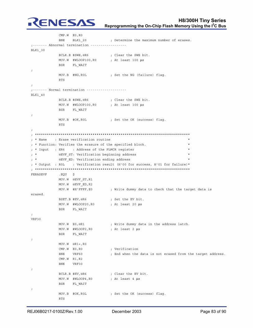
H8/300H Tiny SeriesReprogramming the On-Chip Flash Memory Using the I2C Bus
REJ06B0217-0100Z/Rev.1.00 December 2003 Page 83 of 90
CMP.W E0,R0
BNE BLK1_20 ; Determine the maximum number of erases.
;------- Abnormal termination ------------------
BLK1_30
BCLR.B #SWE,@R6 ; Clear the SWE bit.
MOV.W #WLOOP100,R0 ; At least 100 µs BSR FL_WAIT
;
MOV.B #NG,R0L ; Set the NG (failure) flag.
RTS
;
;------- Normal termination --------------------
BLK1_40
BCLR.B #SWE,@R6 ; Clear the SWE bit.
MOV.W #WLOOP100,R0 ; At least 100 µs BSR FL_WAIT
;
MOV.B #OK,R0L ; Set the OK (success) flag.
RTS
;
; ******************************************************************************
; * Name : Erase verification routine *
; * Function: Verifies the erasure of the specified block. *
; * Input : ER6 : Address of the FLMCR register *
; * @EVF_ST: Verification beginning address *
; * @EVF_ED: Verification ending address *
; * Output : R0L : Verification result (H'00 for success, H'01 for failure)*
; ******************************************************************************
FERASEVF .EQU $
MOV.W @EVF_ST,R1
MOV.W @EVF_ED,R2
MOV.W #H'FFFF,E0 ; Write dummy data to check that the target data is
erased.
BSET.B #EV,@R6 ; Set the EV bit.
MOV.W #WLOOP20,R0 ; At least 20 µs BSR FL_WAIT
;
VRF30
MOV.W E0,@R1 ; Write dummy data in the address latch.
MOV.W #WLOOP2,R0 ; At least 2 µs BSR FL_WAIT
;
MOV.W @R1+,R0
CMP.W E0,R0 ; Verification
BNE VRF60 ; End when the data is not erased from the target address.
CMP.W R1,R2
BNE VRF30
;
BCLR.B #EV,@R6 ; Clear the EV bit.
MOV.W #WLOOP4,R0 ; At least 4 µs BSR FL_WAIT
;
MOV.B #OK,R0L ; Set the OK (success) flag.
RTS
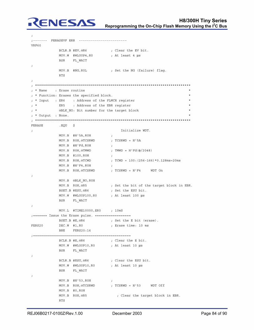
H8/300H Tiny SeriesReprogramming the On-Chip Flash Memory Using the I2C Bus
REJ06B0217-0100Z/Rev.1.00 December 2003 Page 84 of 90
;
;------- FERASEVF ERR ------------------------
VRF60
BCLR.B #EV,@R6 ; Clear the EV bit.
MOV.W #WLOOP4,R0 ; At least 4 µs BSR FL_WAIT
;
MOV.B #NG,R0L ; Set the NG (failure) flag.
RTS
;
; ******************************************************************************
; * Name : Erase routine *
; * Function: Erases the specified block. *
; * Input : ER6 : Address of the FLMCR register *
; * ER5 : Address of the EBR register *
; * @BLK_NO: Bit number for the target block *
; * Output : None. *
; ******************************************************************************
FERASE .EQU $
; Initialize WDT.
MOV.B #H'5A,R0H ;
MOV.B R0H,@TCSRWD ; TCSRWD = H'5A
MOV.B #H'Fd,R0H ;
MOV.B R0H,@TMWD ; TMWD = H'Fd(φ/2048) MOV.B #100,R0H ;
MOV.B R0H,@TCWD ; TCWD = 100:(256-166)*0.128ms=20ms
MOV.B #H'F4,R0H ;
MOV.B R0H,@TCSRWD ; TCSRWD = H'F4 WDT On
;
MOV.B @BLK_NO,R0H
MOV.B R0H,@R5 ; Set the bit of the target block in EBR.
BSET.B #ESU,@R6 ; Set the ESU bit.
MOV.W #WLOOP100,R0 ; At least 100 µs BSR FL_WAIT
;
MOV.L #TIME10000,ER0 ; 10mS
;======= Issue the Erase pulse. ==================
BSET.B #E,@R6 ; Set the E bit (erase).
FERS20 DEC.W #1,R0 ; Erase time: 10 ms
BNE FERS20:16
;=================================================
BCLR.B #E,@R6 ; Clear the E bit.
MOV.W #WLOOP10,R0 ; At least 10 µs BSR FL_WAIT
;
BCLR.B #ESU,@R6 ; Clear the ESU bit.
MOV.W #WLOOP10,R0 ; At least 10 µs BSR FL_WAIT
;
MOV.B #H'53,R0H ;
MOV.B R0H,@TCSRWD ; TCSRWD = H'53 WDT Off
MOV.B #0,R0H
MOV.B R0H,@R5 ; Clear the target block in EBR.
RTS

H8/300H Tiny SeriesReprogramming the On-Chip Flash Memory Using the I2C Bus
REJ06B0217-0100Z/Rev.1.00 December 2003 Page 85 of 90
;
;==========Wait subroutine========================
FL_WAIT DEC.W #1,R0
BNE FL_WAIT
RTS
;=================================================
File: vect.src
;**********************************************************/
; Vector Table */
;**********************************************************/
.IMPORT _INIT
.IMPORT VTRAP0,VTRAP1,VTRAP2,VTRAP3
.IMPORT VBRAK,VSLEP
.IMPORT VIRQ0,VIRQ1,VIRQ2,VIRQ3
.IMPORT VWKP,VOVRF
.IMPORT VTMRW,VTMRV
.IMPORT VSCI3,VIIC,VADC
;
.SECTION V0,CODE,LOCATE=H'0000
;************************************************************/
; adrs
;************************************************************/
.DATA.W _INIT ; 00 RESET VECTER ADDRESS
;
.SECTION V1,CODE,LOCATE=H'0010
.DATA.W VTRAP0 ; 10 TRAP#0
.DATA.W VTRAP1 ; 12 TRAP#1
.DATA.W VTRAP2 ; 14 TRAP#2
.DATA.W VTRAP3 ; 16 TRAP#3
.DATA.W VBRAK ; 18 BREAK
.DATA.W VSLEP ; 1A SLEEP
.DATA.W VIRQ0 ; 1C IRQ0
.DATA.W VIRQ1 ; 1E IRQ1
.DATA.W VIRQ2 ; 20 IRQ2
.DATA.W VIRQ3 ; 22 IRQ3
.DATA.W VWKP ; 24 WKP
.DATA.W VOVRF ; 26 OVER FLOW
;
.SECTION V2,CODE,LOCATE=H'002A
.DATA.W VTMRW ; 2A TIMER W
.DATA.W VTMRV ; 2C TIMER V
.DATA.W VSCI3 ; 2E SCI3_RX/TX/ERR
.DATA.W VIIC ; 30 IIC
.DATA.W VADC ; 32 ADC
;************************************************************/
.END

H8/300H Tiny SeriesReprogramming the On-Chip Flash Memory Using the I2C Bus
REJ06B0217-0100Z/Rev.1.00 December 2003 Page 86 of 90
File: u_vect.src
;**********************************************************/
; User Vector Table */
;**********************************************************/
.IMPORT _INIT
.EXPORT VTRAP0,VTRAP1,VTRAP2,VTRAP3
.EXPORT VBRAK,VSLEP
.EXPORT VIRQ0,VIRQ1,VIRQ2,VIRQ3
.EXPORT VWKP,VOVRF
.EXPORT VTMRW,VTMRV
.EXPORT VSCI3,VIIC,VADC
;
.SECTION UV,CODE,LOCATE=H'1000
;************************************************************/
; Jump to user_program
;************************************************************/
VTRAP0:
JMP @_INIT
VTRAP1:
JMP @_INIT
VTRAP2:
JMP @_INIT
VTRAP3:
JMP @_INIT
VBRAK:
JMP @_INIT
VSLEP:
JMP @_INIT
VIRQ0:
JMP @_INIT
VIRQ1:
JMP @_INIT
VIRQ2:
JMP @_INIT
VIRQ3:
JMP @_INIT
VWKP:
JMP @_INIT
VOVRF:
JMP @_INIT
VTMRW:
JMP @_INIT
VTMRV:
JMP @_INIT
VSCI3:
JMP @_INIT
VIIC:
JMP @_INIT
VADC:
JMP @_INIT
;************************************************************/
.END
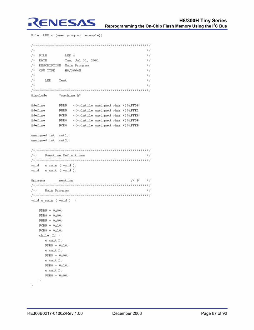
H8/300H Tiny SeriesReprogramming the On-Chip Flash Memory Using the I2C Bus
REJ06B0217-0100Z/Rev.1.00 December 2003 Page 87 of 90
File: LED.c (user program (example))
/**********************************************************/
/* */
/* FILE :LED.c */
/* DATE :Tue, Jul 31, 2001 */
/* DESCRIPTION :Main Program */
/* CPU TYPE :H8/3664N */
/* */
/* LED Test */
/* */
/**********************************************************/
#include "machine.h"
#define PDR5 *(volatile unsigned char *)0xFFD8
#define PMR5 *(volatile unsigned char *)0xFFE1
#define PCR5 *(volatile unsigned char *)0xFFE8
#define PDR8 *(volatile unsigned char *)0xFFDB
#define PCR8 *(volatile unsigned char *)0xFFEB
unsigned int cnt1;
unsigned int cnt2;
/*;********************************************************/
/*; Function Definitions */
/*;********************************************************/
void u_main ( void );
void u_wait ( void );
#pragma section /* P */
/*;********************************************************/
/*; Main Program */
/*;********************************************************/
void u_main ( void )
PDR5 = 0x00;
PDR8 = 0x00;
PMR5 = 0x00;
PCR5 = 0x10;
PCR8 = 0x10;
while (1)
u_wait();
PDR5 = 0x10;
u_wait();
PDR5 = 0x00;
u_wait();
PDR8 = 0x10;
u_wait();
PDR8 = 0x00;
H8/300H Tiny SeriesReprogramming the On-Chip Flash Memory Using the I2C Bus
REJ06B0217-0100Z/Rev.1.00 December 2003 Page 88 of 90
/*;********************************************************/
/*; Sub Program */
/*;********************************************************/
void u_wait(void)
cnt1 = 0;
cnt2 = 0;
while (cnt2 < 1000)
while (cnt1 < 300)
cnt1++;
cnt2++;
cnt1 = 0;

H8/300H Tiny SeriesReprogramming the On-Chip Flash Memory Using the I2C Bus
REJ06B0217-0100Z/Rev.1.00 December 2003 Page 89 of 90
Revision RecordDescription
Rev. Date Page Summary1.00 Dec.20.03 — First edition issued

H8/300H Tiny SeriesReprogramming the On-Chip Flash Memory Using the I2C Bus
REJ06B0217-0100Z/Rev.1.00 December 2003 Page 90 of 90
1. These materials are intended as a reference to assist our customers in the selection of the Renesas Technology Corp. product best suited to the customer's application; they do not convey any license under any intellectual property rights, or any other rights, belonging to Renesas Technology Corp. or a third party.
2. Renesas Technology Corp. assumes no responsibility for any damage, or infringement of any third-party's rights, originating in the use of any product data, diagrams, charts, programs, algorithms, or circuit application examples contained in these materials.
3. All information contained in these materials, including product data, diagrams, charts, programs and algorithms represents information on products at the time of publication of these materials, and are subject to change by Renesas Technology Corp. without notice due to product improvements or other reasons. It is therefore recommended that customers contact Renesas Technology Corp. or an authorized Renesas Technology Corp. product distributor for the latest product information before purchasing a product listed herein.The information described here may contain technical inaccuracies or typographical errors.Renesas Technology Corp. assumes no responsibility for any damage, liability, or other loss rising from these inaccuracies or errors.Please also pay attention to information published by Renesas Technology Corp. by various means, including the Renesas Technology Corp. Semiconductor home page (http://www.renesas.com).
4. When using any or all of the information contained in these materials, including product data, diagrams, charts, programs, and algorithms, please be sure to evaluate all information as a total system before making a final decision on the applicability of the information and products. Renesas Technology Corp. assumes no responsibility for any damage, liability or other loss resulting from the information contained herein.
5. Renesas Technology Corp. semiconductors are not designed or manufactured for use in a device or system that is used under circumstances in which human life is potentially at stake. Please contact Renesas Technology Corp. or an authorized Renesas Technology Corp. product distributor when considering the use of a product contained herein for any specific purposes, such as apparatus or systems for transportation, vehicular, medical, aerospace, nuclear, or undersea repeater use.
6. The prior written approval of Renesas Technology Corp. is necessary to reprint or reproduce in whole or in part these materials.
7. If these products or technologies are subject to the Japanese export control restrictions, they must be exported under a license from the Japanese government and cannot be imported into a country other than the approved destination.Any diversion or reexport contrary to the export control laws and regulations of Japan and/or the country of destination is prohibited.
8. Please contact Renesas Technology Corp. for further details on these materials or the products contained therein.
1. Renesas Technology Corp. puts the maximum effort into making semiconductor products better and more reliable, but there is always the possibility that trouble may occur with them. Trouble with semiconductors may lead to personal injury, fire or property damage.Remember to give due consideration to safety when making your circuit designs, with appropriate measures such as (i) placement of substitutive, auxiliary circuits, (ii) use of nonflammable material or (iii) prevention against any malfunction or mishap.
Keep safety first in your circuit designs!
Notes regarding these materials