research article a wide tuning-range cmos vco with a...
TRANSCRIPT

Research ArticleA Wide Tuning-Range CMOS VCO witha Tunable Active Inductor
Hsuan-Ling Kao Ping-Che Lee and Hsien-Chin Chiu
Department of Electronic Engineering Chang Gung University Taoyuan City 33302 Taiwan
Correspondence should be addressed to Hsuan-Ling Kao snoopymailcguedutw
Received 9 August 2014 Accepted 26 December 2014
Academic Editor Zhenhai Shao
Copyright copy 2015 Hsuan-Ling Kao et al This is an open access article distributed under the Creative Commons AttributionLicense which permits unrestricted use distribution and reproduction in any medium provided the original work is properlycited
This study describes a wide tuning-range VCO using tunable active inductor (TAI) topology and cross-coupled pair configurationfor radio frequency operation The TAI used two feedback loops to form a cascode circuit to obtain more degrees of freedom forinductance value The TAI-VCO was fabricated using a 018120583m CMOS technology The coarse frequency tuning is achieved byTAIs while the fine tuning is controlled by varactorsThe fabricated circuit provides an output frequency range from 06 to 72GHz(169)Themeasured phase noise is from minus11038 to minus8601 dBcHz at a 1MHz offset and output power is from minus1111 to minus389 dBmwithin the entire frequency range under a 18 V power supply
1 Introduction
The rapidly developing wireless and communication sys-tems make the multiband RF terminals from several hun-dred megahertz to gigahertz frequency coexist Integratedmultiband wireless blocks in one-chip IC are demandedfor high-speed high-functionality small-size and low-costcommunication systems One of the key building blocks isfully integrated voltage controlled oscillators (VCOs) Thechallenges of the VCO circuit are die size cost and powerdissipation The general VCO circuits used spiral inductorsand varactors to realize the circuit However the on-chipspiral inductors have a small inductance value per unit areaand low 119876-factor because of losses of Si-substrate It alsooccupied a large chip size The varactors limited the tuningrange within 30 due to the maximum to the minimumcapacitance ratio of the varactor and the parasitic effect [1ndash3]Therefore various techniques have been proposed to enhancethe tuning range of VCOs such as switched capacitor arrays[4ndash8] switched inductors [9ndash11] and tunable active inductors(TAIs) [12ndash16] TAI is one of the good candidates due toits small size high 119876 widely tunable inductance and largeinductance compared to those of the spiral inductor [17 18]The tuning range of 120 (05sim2GHz) is achieved in a single-end VCO circuit with a TAI tuned by tunable feedbackresistance [14] A differential TAI is proposed to achieve
a 05sim3GHz (143) tuning range andminus118 dBcHz at a 1MHzoffset at 690MHz [15] However the operation frequenciesare lower than 3GHz because the traditional active inductoris difficult to operate at higher frequency due to a largeparasitic load capacitance The cascode active inductor (AI)is proposed to enhance the resonance frequency [17] Inthis study by utilizing a tunable cascade active inductor theVCO circuit exhibits a very wide frequency tuning rangeand also enhances output power and phase noise The TAI-VCO provides an output frequency which ranges from 06 to72GHz (169) The paper is organized as follows Section 2outlines tunable active inductor design Section 3 presentsthe TAI-VCO circuit design Section 4 presents the TAI-VCOmeasurement results Finally concluding remarks are offered
2 Tunable Active Inductor Design
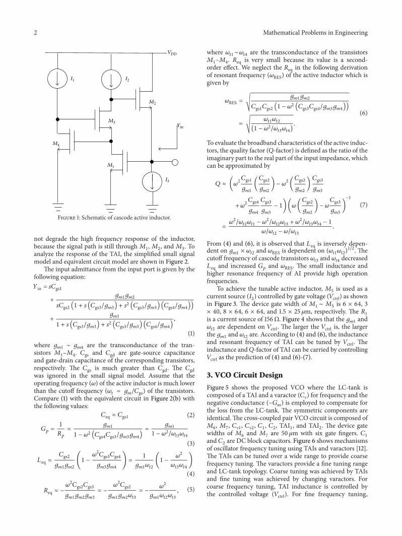
Figure 1 shows that the proposed AI circuit consists of fourtransistors (119872
1sim 1198724) and three current sources (119868
1sim 1198683)
Two feedback loops are formed in this circuit Transistors1198721and 119872
2make up the first feedback loop and 119872
3and
1198724form the second loop The cascode technique is used to
reduce output conductance and enhance the gain for highfrequency Transistor119872
3is stacked on top of transistor119872
1
For increasing the cascode effect the additional gain stagewas implemented by119872
4 The addition of transistor119872
4does
Hindawi Publishing CorporationMathematical Problems in EngineeringVolume 2015 Article ID 382483 7 pageshttpdxdoiorg1011552015382483
2 Mathematical Problems in Engineering
I1 I2
I3
M1
M2
M3
M4
Yin
VDD
Figure 1 Schematic of cascode active inductor
not degrade the high frequency response of the inductorbecause the signal path is still through119872
11198722 and119872
3 To
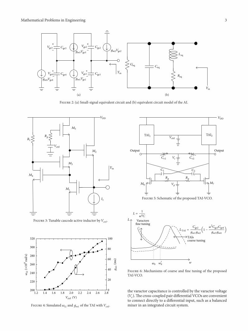
analyze the response of the TAI the simplified small signalmodel and equivalent circuit model are shown in Figure 2
The input admittance from the input port is given by thefollowing equation119884in = 119904119862gs1
+11989211989811198921198982
119904119862gs2 (1 + 119904 (119862gs31198921198983) + 1199042 (119862gs31198921198983) (119862gs41198921198984))
+1198921198981
1 + 119904 (119862gs31198921198983) + 1199042 (119862gs31198921198983) (119862gs41198921198984)
(1)
where 1198921198981sim 1198921198984
are the transconductance of the tran-sistors 119872
1ndash1198724 119862gs and 119862gd are gate-source capacitance
and gate-drain capacitance of the corresponding transistorsrespectively The 119862gs is much greater than 119862gd The 119862gdwas ignored in the small signal model Assume that theoperating frequency (120596) of the active inductor is much lowerthan the cutoff frequency (120596
119905= 119892119898119862gs) of the transistors
Compare (1) with the equivalent circuit in Figure 2(b) withthe following values
119862eq asymp 119862gs1 (2)
119866119901=1
119877119901
asymp1198921198981
1 minus 1205962 (119862gs4119862gs311989211989831198921198984)=
1198921198981
1 minus 120596212059611990531205961199054
(3)
119871eq asymp119862gs2
11989211989811198921198982
(1 minus1205962119862gs3119862gs4
11989211989831198921198984
) =1
11989211989811205961199052
(1 minus1205962
12059611990531205961199054
)
(4)
119877eq asymp minus1205962119862gs2119862gs3
119892119898111989211989821198921198983
= minus1205962119862gs2
119892119898111989211989821205961199053
= minus1205962
119892119898112059611990521205961199053
(5)
where 1205961199051sim1205961199054are the transconductance of the transistors
1198721ndash1198724 119877eq is very small because its value is a second-
order effect We neglect the 119877eq in the following derivationof resonant frequency (120596RES) of the active inductor which isgiven by
120596RES = radic11989211989811198921198982
119862gs1119862gs2 (1 minus 1205962 (119862gs3119862gs411989211989831198921198984))
= radic12059611990511205961199052
(1 minus 120596212059611990531205961199054)
(6)
To evaluate the broadband characteristics of the active induc-tors the quality factor (119876-factor) is defined as the ratio of theimaginary part to the real part of the input impedance whichcan be approximated by
119876 asymp (1205962119862gs1
1198921198981
(119862gs2
1198921198982
) minus 1205962(119862gs2
1198921198982
)119862gs3
1198921198983
+1205962119862gs4
1198921198984
119862gs3
1198921198983
minus 1)(120596(119862gs2
1198921198982
) minus 120596119862gs3
1198921198983
)
minus1
=120596212059611990521205961199051minus 120596212059611990521205961199053+ 120596212059611990531205961199054minus 1
1205961205961199052minus 120596120596
1199053
(7)
From (4) and (6) it is observed that 119871eq is inversely depen-dent on 119892
1198981times 1205961199052and 120596RES is dependent on (12059611990511205961199052)
12 Thecutoff frequency of cascode transistors 120596
1199053and 120596
1199054decreased
119871eq and increased 119866119901and 120596RES The small inductance and
higher resonance frequency of AI provide high operationfrequencies
To achieve the tunable active inductor 1198725is used as a
current source (1198682) controlled by gate voltage (119881ctrl) as shown
in Figure 3 The device gate width of 1198721sim 1198725is 6 times 64 3
times 40 8 times 64 6 times 64 and 15 times 25 120583m respectively The 1198771
is a current source of 156Ω Figure 4 shows that the 1198921198981
and1205961199052are dependent on 119881ctrl The larger the 119881ctrl is the larger
the 1198921198981
and 1205961199052are According to (4) and (6) the inductance
and resonant frequency of TAI can be tuned by 119881ctrl Theinductance and119876-factor of TAI can be carried by controlling119881ctrl as the prediction of (4) and (6)-(7)
3 VCO Circuit Design
Figure 5 shows the proposed VCO where the LC-tank iscomposed of a TAI and a varactor (119862V) for frequency and thenegative conductance (minus119866
119898) is employed to compensate for
the loss from the LC-tank The symmetric components areidenticalThe cross-coupled pair VCO circuit is composed of1198726 1198727 119862V1 119862V2 1198621 1198622 TAI1 and TAI
2 The device gate
widths of 1198726and 119872
7are 50 120583m with six gate fingers 119862
1
and 1198622are DC block capacitors Figure 6 shows mechanisms
of oscillator frequency tuning using TAIs and varactors [12]The TAIs can be tuned over a wide range to provide coarsefrequency tuning The varactors provide a fine tuning rangeand LC-tank topology Coarse tuning was achieved by TAIsand fine tuning was achieved by changing varactors Forcoarse frequency tuning TAI inductance is controlled bythe controlled voltage (119881ctrl) For fine frequency tuning
Mathematical Problems in Engineering 3
Vgs3
Vgs1
Vgs2Cgs3
Cgs1
Cgs2
Cgs4
gm2Vgs2
Yin
gm1Vgs1gm4Vgs4
gm3Vgs3
Vgs4
+ +
+ +
minus minus
minus minus
(a)
Geq Ceq
Req
Leq
Yin
(b)
Figure 2 (a) Small-signal equivalent circuit and (b) equivalent circuit model of the AI
R1
Rg
Vctrl
VDD
I1
Yin
M1
M2
M3
M4
M5
Figure 3 Tunable cascode active inductor by 119881ctrl
0
20
40
60
80
100
12 14 16 18 20 22 24 26 28200
220
240
260
280
300
320
120596t2
(times109
rad
s)
Vctrl (V)
gm1
(ms)
Figure 4 Simulated 1205961199052and 119892
1198981of the TAI with 119881ctrl
TAI1 TAI2
Rg Rg
VDD
Vctrl
Output Output
C1 C2Vc
C1 C2
M6M7Vg
Figure 5 Schematic of the proposed TAI-VCO
L =1
1205962C
Varactorsfine tuning
TAIscoarse tuning
1205960 1205969984000
120596
L
LTAI =Cgs2
gm1gm2
(1 minus 1205962Cgs3Cgs4
gm3gm4
)
Figure 6 Mechanisms of coarse and fine tuning of the proposedTAI-VCO
the varactor capacitance is controlled by the varactor voltage(119881119888)The cross-coupled pair differential VCOs are convenient
to connect directly to a differential input such as a balancedmixer in an integrated circuit system
4 Mathematical Problems in Engineering
The noise current injected at output nodes is composedof two parts 1198942
119899TAI and 1198942119899CC representing the contribution ofTAI and cross-coupled pair (CC) transistors respectivelyThenoise current typically is the channel-induced noise and gate-induced noise of a transistorThe total noise current of outputnodes can be written as
1198942119899total
Δ119891= 21198942119899TAI
Δ119891+1198942119899CC
Δ119891 (8)
The total single-sideband phase noise spectral density at anoffset frequency of Δ120596 is given by
119871 Δ120596 = 10 log(suminfin
119899=01198621198991198942119899totalΔ119891
41199022maxΔ1205962
) (9)
where 119862119899represents the coefficients in the Fourier series of
the impulse sensitivity function and 119902max is the maximumcharge swing across the current noise source The TAI andCC are composed of five and two transistors respectivelyThe phase noise of TAI-VCO is larger than LC-VCO dueto the number of transistors However the output power isalso an important parameter of VCO The coarse frequencytuning of the cascode TAI was controlled by 119881ctrl As 119881ctrlincreases 119872
5was driven from triode region to saturation
region resulting in larger bias current and larger drain voltagefor the cross-coupled pair Therefore the larger drain voltageof the cross-coupled pair provided larger output swing athigher frequencywhile decreasing equivalent inductance andincreasing oscillation frequency A uniformoutput power canbe achieved over the whole frequency range in the proposedTAI-VCO topology
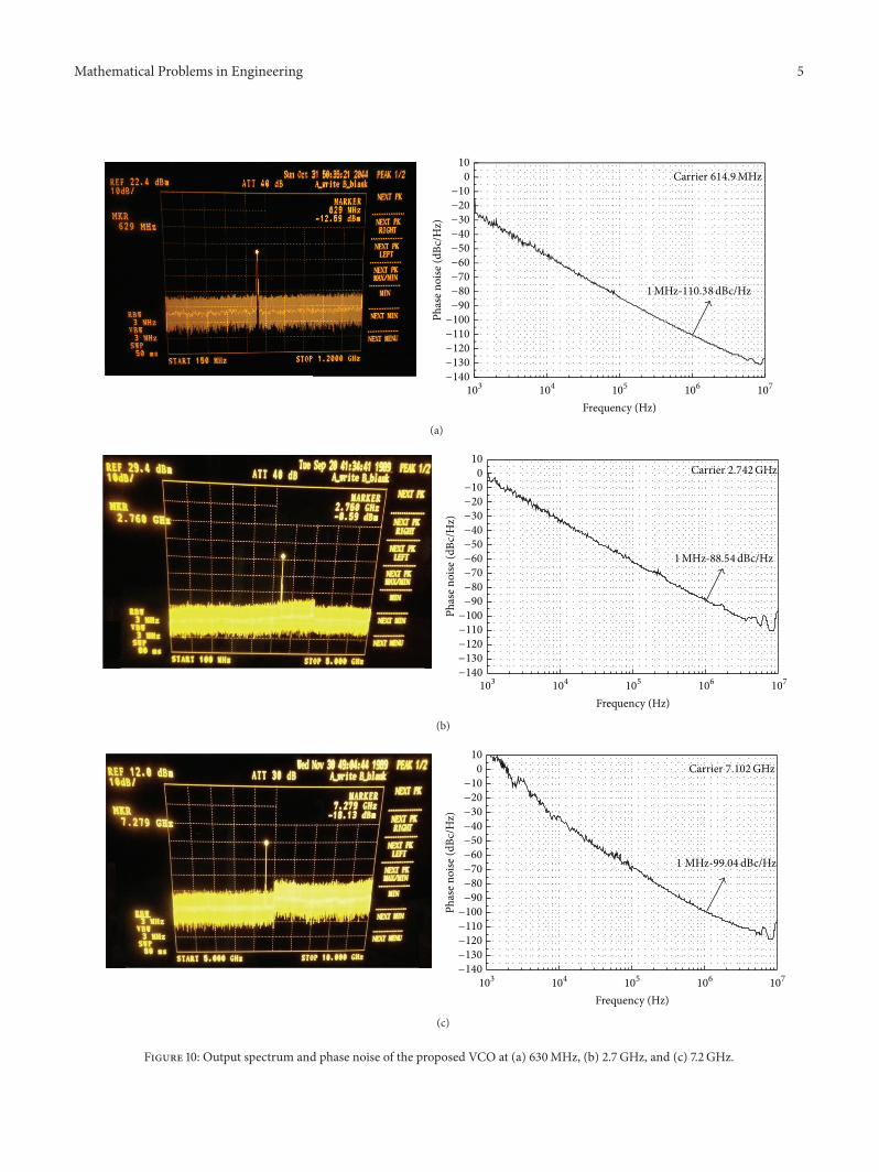
4 Measurement Results
The cross-coupled pair VCO was simulated using AdvanceDesign System (ADS) software The layout of the circuitespecially the symmetry of the cross-coupled design playsan important role in circuit design The top-layer metal andbottom-layer metal crossing and the difference between pathlengths are crucial to ensure balanced signals and a compactsize Figure 7 shows the layout of the fabricated VCO Its sizeis 0835times 0615mm2 including the probe padsTheTAI-VCOwas tested on awafermdashthe spectral density of the circuit beingmeasured with a spectrum analyzer The circuit is biased at119881DD = 18V119881119892 = 07V 119868total = 23sim27mA119881ctrl = 14sim27Vand 119881
119888= 05 sim 20V The power consumption of the VCO is
41sim49mW from a 18 V power supplyFigure 8 shows the tuning range of the TAI-VCO circuit
The proposed cross-coupled pair VCO was tuned from06GHz to 72GHz which is a tuning range of 65 GHz(near 169 tuning range) Figure 9 shows the phase noiseand output power of the TAI-VCO circuit The VCO hasphase noise of minus11038 and minus9904 dBcHz at a 1MHzoffset from 063 and 72GHz carrier respectively Withinthe VCO tuning range the variations in output power areminus764 plusmn 35 dBm The output spectrum and phase noise ofthe proposedTAI-VCOat 630MHz 27 GHz and 72GHz are
0835mm
0615mm
G
S
G
G
S
G
P GP PG
P
PGPPGP
Figure 7 Photograph of the fabricated VCO
0608
1012
1416
1820
0
1
2
3
4
5
6
7
8
1416
182022242628
Freq
uenc
y (G
Hz)
Vctrl
(V)
Vc (V)
Figure 8 Measured oscillation frequency against 119881ctrl and 119881119888
12 14 16 18 20 22 24 26 28minus50
minus45
minus40
minus35
minus30
minus25
minus20
minus15
minus10
minus5
0
5
10
minus130
minus120
minus110
minus100
minus90
minus80
minus70
minus60
minus50
minus40
Pou
t(d
Bm)
Vctrl (V)
Phase noise
Pout
Phas
e noi
se at
1M
Hz (
dBc
Hz)
Figure 9 Measured phase noise and output power against controlvoltage 119881ctrl
shown in Figure 10The lowest phase noise isminus11038 dBcHzat 1MHz offset from the 0629GHz carrier frequency Themaximumoutput power is minus389 dBm including a 47 dB lossdue to implementation and operates at 27 GHz under a 18 Vpower supply Table 1 summarizes themeasured performance
Mathematical Problems in Engineering 5
minus140
minus130
minus120
minus110
minus100
minus90
minus80
minus70
minus60
minus50
minus40
minus30
minus20
minus10
0
10
103 104 105 106 107
1MHz-11038dBcHz
Phas
e noi
se (d
BcH
z)
Frequency (Hz)
Carrier 6149MHz
(a)
Carrier 2742GHz
1MHz-8854dBcHz
minus140
minus130
minus120
minus110
minus100
minus90
minus80
minus70
minus60
minus50
minus40
minus30
minus20
minus10
0
10
103 104 105 106 107
Phas
e noi
se (d
BcH
z)
Frequency (Hz)
(b)
Carrier 7102GHz
1 MHz-9904dBcHz
minus140
minus130
minus120
minus110
minus100
minus90
minus80
minus70
minus60
minus50
minus40
minus30
minus20
minus10
0
10
103 104 105 106 107
Phas
e noi
se (d
BcH
z)
Frequency (Hz)
(c)
Figure 10 Output spectrum and phase noise of the proposed VCO at (a) 630MHz (b) 27 GHz and (c) 72 GHz
6 Mathematical Problems in Engineering
Table 1 Comparison of VCO circuit performance published and this work
Unit This work [7] [8] [9] [13] [14] [15] [16]lowast
Tuning range GHz 06sim72 32sim53 33sim51 11sim19 11sim27 05sim2 05sim3 13sim22 169 477 411 51 81 120 143 475
KVCO MHzV 5000 167sim555 50sim85 667 3850 500 2500 458119875out dBm minus389simminus111 minus48 minus7 mdash minus1428 minus21simminus29 minus14simminus22 minus9simminus16PN at 1MHz offset dBcHz minus86simminus110 minus1156 minus12314 minus126 minus83simminus92 minus78simminus90 minus101simminus118 minus82simminus86Area mm2 051 0828 024 05 04 009 045 mdash
Architecture TAI Switched-cap Switched-cap Switched-ind TAI TAI TAI TAIlowastSimulated results
of theVCOand includes other reported performances for thepurpose of comparison [7ndash9 13ndash16]
5 Conclusion
The fully integrated VCO with tunable active inductor on018 120583m CMOS technology demonstrated good circuit per-formance in terms of a wide tuning range high outputpower and low phase noise This TAI-VCO displayed a widefrequency range from 06 to 72GHz resulting in a tuningrange of 169 at radio frequency The lowest phase noise wasminus11038 dBcHz at a 1MHz offset from a 630MHz carrier anda highest output power of minus389 dBm at 27 GHz under a 18 Vpower supply
Conflict of Interests
The authors declare that there is no conflict of interestsregarding the publication of this paper
Acknowledgments
The authors wish to thank CIC of the National ScienceCouncil and the High Speed Intelligent CommunicationResearchCenter atChangGungUniversity for their helpThiswork was partially supported by the Ministry of Science andTechnology of Taiwan (no 103-2221-E-182 -009)
References
[1] M Li R E Amaya R G Harrison and N G Tarr ldquoInvesti-gation of CMOS varactors for high-GHz-range applicationsrdquoResearch Letters in Electronics vol 2009 Article ID 535809 4pages 2009
[2] L Jia J G Ma K S Yeo X P Yu M A Do and W M LimldquoA 18-V 24515-GHz dual-band LCVCO in 018-120583m CMOStechnologyrdquo IEEE Microwave and Wireless Components Lettersvol 16 no 4 pp 194ndash196 2006
[3] B Min and H Jeong ldquo5-GHz CMOS LC VCOs with widetuning rangesrdquo IEEE Microwave and Wireless ComponentsLetters vol 15 no 5 pp 336ndash338 2005
[4] Y J Moon Y S Roh C Y Jeong and C Yoo ldquoA 439526 ghzLC-tank CMOS voltage-controlled oscillator with small VCO-gain variationrdquo IEEE Microwave and Wireless ComponentsLetters vol 19 no 8 pp 524ndash526 2009
[5] S-L Liu K-H Chen and A Chin ldquoA dual-resonant mode1022-GHz VCO with a novel inductive switching approachrdquoIEEETransactions onMicrowaveTheory and Techniques vol 60no 7 pp 2165ndash2177 2012
[6] Y Ito K Okada and K Masu ldquoA tunable wideband frequencysynthesizer using LC-VCO and mixer for reconfigurable radiotransceiversrdquo Journal of Electrical and Computer Engineeringvol 2011 Article ID 361910 7 pages 2011
[7] T-P Wang and S-Y Wang ldquoA low-voltage low-power low-phase-noise wide-tuning-range 018-120583m CMOS VCO withhigh-performance FOMT of ndash1963 dBcHzrdquo in Proceedings ofthe IEEE MTT-S International Microwave Symposium Digest(MTT 13) pp 1ndash4 Seattle Wash USA June 2013
[8] H Yoon Y Lee J J Kim and J Choi ldquoA wideband dual-mode LC-VCO with a switchable gate-biased active corerdquo IEEETransactions on Circuits and Systems II Express Briefs vol 61no 5 pp 289ndash293 2014
[9] A Italia C M Ippolito and G Palmisano ldquoA 1-mW 113ndash19GHz CMOS LC VCO using shunt-connected switched-coupled inductorsrdquo IEEE Transactions on Circuits and SystemsI Regular Papers vol 59 no 6 pp 1145ndash1155 2012
[10] F Cernoia D Ponton P Palestri et al ldquoDesign and imple-mentation of switched coil LC-VCOs in the GHz range usingthe self-inductance techniquerdquo International Journal of CircuitTheory and Applications 2013
[11] W Zou X Chen K Dai and X Zou ldquoSwitched-inductor VCObased on tapped vertical solenoid inductorsrdquo Electronics Lettersvol 48 no 9 pp 509ndash511 2012
[12] G Huang and B-S Kim ldquoProgrammable active inductor-basedwideband VCOQVCO designrdquo IET Microwaves Antennas ampPropagation vol 2 no 8 pp 830ndash838 2008
[13] Y J Jeong Y M Kim H J Chang and T Y Yun ldquoLow-powerCMOS VCO with a low-current high-Q active inductorrdquo IETMicrowaves Antennas and Propagation vol 6 no 7 pp 788ndash792 2012
[14] L-H Lu H-H Hsieh and Y-T Liao ldquoA wide tuning-rangeCMOS VCO with a differential tunable active inductorrdquo IEEETransactions on Microwave Theory and Techniques vol 54 no9 pp 3462ndash3468 2006
[15] R Mukhopadhyay Y Park P Sen et al ldquoReconfigurable RFICsin Si-based technologies for a compact intelligent RF front-endrdquoIEEE Transactions onMicrowaveTheory and Techniques vol 53no 1 pp 81ndash93 2005
[16] G Szczepkowski G Baldwin and R Farrell ldquoWideband018 120583m CMOS VCO using active inductor with negativeresistancerdquo in Proceedings of the European Conference on CircuitTheory and Design (ECCTD rsquo07) pp 990ndash993 August 2007
Mathematical Problems in Engineering 7
[17] A Thanachayanont and A Payne ldquoVHF CMOS integratedactive inductorrdquo Electronics Letters vol 32 no 11 pp 999ndash10001996
[18] S V Krishnamurthy K El-Sankary and E El-Masry ldquoNoise-cancelling CMOS active inductor and its application in RFband-pass filter designrdquo International Journal of MicrowaveScience and Technology vol 2010 Article ID 980957 8 pages2010
Submit your manuscripts athttpwwwhindawicom
Hindawi Publishing Corporationhttpwwwhindawicom Volume 2014
MathematicsJournal of
Hindawi Publishing Corporationhttpwwwhindawicom Volume 2014
Mathematical Problems in Engineering
Hindawi Publishing Corporationhttpwwwhindawicom
Differential EquationsInternational Journal of
Volume 2014
Applied MathematicsJournal of
Hindawi Publishing Corporationhttpwwwhindawicom Volume 2014
Probability and StatisticsHindawi Publishing Corporationhttpwwwhindawicom Volume 2014
Journal of
Hindawi Publishing Corporationhttpwwwhindawicom Volume 2014
Mathematical PhysicsAdvances in
Complex AnalysisJournal of
Hindawi Publishing Corporationhttpwwwhindawicom Volume 2014
OptimizationJournal of
Hindawi Publishing Corporationhttpwwwhindawicom Volume 2014
CombinatoricsHindawi Publishing Corporationhttpwwwhindawicom Volume 2014
International Journal of
Hindawi Publishing Corporationhttpwwwhindawicom Volume 2014
Operations ResearchAdvances in
Journal of
Hindawi Publishing Corporationhttpwwwhindawicom Volume 2014
Function Spaces
Abstract and Applied AnalysisHindawi Publishing Corporationhttpwwwhindawicom Volume 2014
International Journal of Mathematics and Mathematical Sciences
Hindawi Publishing Corporationhttpwwwhindawicom Volume 2014
The Scientific World JournalHindawi Publishing Corporation httpwwwhindawicom Volume 2014
Hindawi Publishing Corporationhttpwwwhindawicom Volume 2014
Algebra
Discrete Dynamics in Nature and Society
Hindawi Publishing Corporationhttpwwwhindawicom Volume 2014
Hindawi Publishing Corporationhttpwwwhindawicom Volume 2014
Decision SciencesAdvances in
Discrete MathematicsJournal of
Hindawi Publishing Corporationhttpwwwhindawicom
Volume 2014 Hindawi Publishing Corporationhttpwwwhindawicom Volume 2014
Stochastic AnalysisInternational Journal of
2 Mathematical Problems in Engineering
I1 I2
I3
M1
M2
M3
M4
Yin
VDD
Figure 1 Schematic of cascode active inductor
not degrade the high frequency response of the inductorbecause the signal path is still through119872
11198722 and119872
3 To
analyze the response of the TAI the simplified small signalmodel and equivalent circuit model are shown in Figure 2
The input admittance from the input port is given by thefollowing equation119884in = 119904119862gs1
+11989211989811198921198982
119904119862gs2 (1 + 119904 (119862gs31198921198983) + 1199042 (119862gs31198921198983) (119862gs41198921198984))
+1198921198981
1 + 119904 (119862gs31198921198983) + 1199042 (119862gs31198921198983) (119862gs41198921198984)
(1)
where 1198921198981sim 1198921198984
are the transconductance of the tran-sistors 119872
1ndash1198724 119862gs and 119862gd are gate-source capacitance
and gate-drain capacitance of the corresponding transistorsrespectively The 119862gs is much greater than 119862gd The 119862gdwas ignored in the small signal model Assume that theoperating frequency (120596) of the active inductor is much lowerthan the cutoff frequency (120596
119905= 119892119898119862gs) of the transistors
Compare (1) with the equivalent circuit in Figure 2(b) withthe following values
119862eq asymp 119862gs1 (2)
119866119901=1
119877119901
asymp1198921198981
1 minus 1205962 (119862gs4119862gs311989211989831198921198984)=
1198921198981
1 minus 120596212059611990531205961199054
(3)
119871eq asymp119862gs2
11989211989811198921198982
(1 minus1205962119862gs3119862gs4
11989211989831198921198984
) =1
11989211989811205961199052
(1 minus1205962
12059611990531205961199054
)
(4)
119877eq asymp minus1205962119862gs2119862gs3
119892119898111989211989821198921198983
= minus1205962119862gs2
119892119898111989211989821205961199053
= minus1205962
119892119898112059611990521205961199053
(5)
where 1205961199051sim1205961199054are the transconductance of the transistors
1198721ndash1198724 119877eq is very small because its value is a second-
order effect We neglect the 119877eq in the following derivationof resonant frequency (120596RES) of the active inductor which isgiven by
120596RES = radic11989211989811198921198982
119862gs1119862gs2 (1 minus 1205962 (119862gs3119862gs411989211989831198921198984))
= radic12059611990511205961199052
(1 minus 120596212059611990531205961199054)
(6)
To evaluate the broadband characteristics of the active induc-tors the quality factor (119876-factor) is defined as the ratio of theimaginary part to the real part of the input impedance whichcan be approximated by
119876 asymp (1205962119862gs1
1198921198981
(119862gs2
1198921198982
) minus 1205962(119862gs2
1198921198982
)119862gs3
1198921198983
+1205962119862gs4
1198921198984
119862gs3
1198921198983
minus 1)(120596(119862gs2
1198921198982
) minus 120596119862gs3
1198921198983
)
minus1
=120596212059611990521205961199051minus 120596212059611990521205961199053+ 120596212059611990531205961199054minus 1
1205961205961199052minus 120596120596
1199053
(7)
From (4) and (6) it is observed that 119871eq is inversely depen-dent on 119892
1198981times 1205961199052and 120596RES is dependent on (12059611990511205961199052)
12 Thecutoff frequency of cascode transistors 120596
1199053and 120596
1199054decreased
119871eq and increased 119866119901and 120596RES The small inductance and
higher resonance frequency of AI provide high operationfrequencies
To achieve the tunable active inductor 1198725is used as a
current source (1198682) controlled by gate voltage (119881ctrl) as shown
in Figure 3 The device gate width of 1198721sim 1198725is 6 times 64 3
times 40 8 times 64 6 times 64 and 15 times 25 120583m respectively The 1198771
is a current source of 156Ω Figure 4 shows that the 1198921198981
and1205961199052are dependent on 119881ctrl The larger the 119881ctrl is the larger
the 1198921198981
and 1205961199052are According to (4) and (6) the inductance
and resonant frequency of TAI can be tuned by 119881ctrl Theinductance and119876-factor of TAI can be carried by controlling119881ctrl as the prediction of (4) and (6)-(7)
3 VCO Circuit Design
Figure 5 shows the proposed VCO where the LC-tank iscomposed of a TAI and a varactor (119862V) for frequency and thenegative conductance (minus119866
119898) is employed to compensate for
the loss from the LC-tank The symmetric components areidenticalThe cross-coupled pair VCO circuit is composed of1198726 1198727 119862V1 119862V2 1198621 1198622 TAI1 and TAI
2 The device gate
widths of 1198726and 119872
7are 50 120583m with six gate fingers 119862
1
and 1198622are DC block capacitors Figure 6 shows mechanisms
of oscillator frequency tuning using TAIs and varactors [12]The TAIs can be tuned over a wide range to provide coarsefrequency tuning The varactors provide a fine tuning rangeand LC-tank topology Coarse tuning was achieved by TAIsand fine tuning was achieved by changing varactors Forcoarse frequency tuning TAI inductance is controlled bythe controlled voltage (119881ctrl) For fine frequency tuning
Mathematical Problems in Engineering 3
Vgs3
Vgs1
Vgs2Cgs3
Cgs1
Cgs2
Cgs4
gm2Vgs2
Yin
gm1Vgs1gm4Vgs4
gm3Vgs3
Vgs4
+ +
+ +
minus minus
minus minus
(a)
Geq Ceq
Req
Leq
Yin
(b)
Figure 2 (a) Small-signal equivalent circuit and (b) equivalent circuit model of the AI
R1
Rg
Vctrl
VDD
I1
Yin
M1
M2
M3
M4
M5
Figure 3 Tunable cascode active inductor by 119881ctrl
0
20
40
60
80
100
12 14 16 18 20 22 24 26 28200
220
240
260
280
300
320
120596t2
(times109
rad
s)
Vctrl (V)
gm1
(ms)
Figure 4 Simulated 1205961199052and 119892
1198981of the TAI with 119881ctrl
TAI1 TAI2
Rg Rg
VDD
Vctrl
Output Output
C1 C2Vc
C1 C2
M6M7Vg
Figure 5 Schematic of the proposed TAI-VCO
L =1
1205962C
Varactorsfine tuning
TAIscoarse tuning
1205960 1205969984000
120596
L
LTAI =Cgs2
gm1gm2
(1 minus 1205962Cgs3Cgs4
gm3gm4
)
Figure 6 Mechanisms of coarse and fine tuning of the proposedTAI-VCO
the varactor capacitance is controlled by the varactor voltage(119881119888)The cross-coupled pair differential VCOs are convenient
to connect directly to a differential input such as a balancedmixer in an integrated circuit system
4 Mathematical Problems in Engineering
The noise current injected at output nodes is composedof two parts 1198942
119899TAI and 1198942119899CC representing the contribution ofTAI and cross-coupled pair (CC) transistors respectivelyThenoise current typically is the channel-induced noise and gate-induced noise of a transistorThe total noise current of outputnodes can be written as
1198942119899total
Δ119891= 21198942119899TAI
Δ119891+1198942119899CC
Δ119891 (8)
The total single-sideband phase noise spectral density at anoffset frequency of Δ120596 is given by
119871 Δ120596 = 10 log(suminfin
119899=01198621198991198942119899totalΔ119891
41199022maxΔ1205962
) (9)
where 119862119899represents the coefficients in the Fourier series of
the impulse sensitivity function and 119902max is the maximumcharge swing across the current noise source The TAI andCC are composed of five and two transistors respectivelyThe phase noise of TAI-VCO is larger than LC-VCO dueto the number of transistors However the output power isalso an important parameter of VCO The coarse frequencytuning of the cascode TAI was controlled by 119881ctrl As 119881ctrlincreases 119872
5was driven from triode region to saturation
region resulting in larger bias current and larger drain voltagefor the cross-coupled pair Therefore the larger drain voltageof the cross-coupled pair provided larger output swing athigher frequencywhile decreasing equivalent inductance andincreasing oscillation frequency A uniformoutput power canbe achieved over the whole frequency range in the proposedTAI-VCO topology
4 Measurement Results
The cross-coupled pair VCO was simulated using AdvanceDesign System (ADS) software The layout of the circuitespecially the symmetry of the cross-coupled design playsan important role in circuit design The top-layer metal andbottom-layer metal crossing and the difference between pathlengths are crucial to ensure balanced signals and a compactsize Figure 7 shows the layout of the fabricated VCO Its sizeis 0835times 0615mm2 including the probe padsTheTAI-VCOwas tested on awafermdashthe spectral density of the circuit beingmeasured with a spectrum analyzer The circuit is biased at119881DD = 18V119881119892 = 07V 119868total = 23sim27mA119881ctrl = 14sim27Vand 119881
119888= 05 sim 20V The power consumption of the VCO is
41sim49mW from a 18 V power supplyFigure 8 shows the tuning range of the TAI-VCO circuit
The proposed cross-coupled pair VCO was tuned from06GHz to 72GHz which is a tuning range of 65 GHz(near 169 tuning range) Figure 9 shows the phase noiseand output power of the TAI-VCO circuit The VCO hasphase noise of minus11038 and minus9904 dBcHz at a 1MHzoffset from 063 and 72GHz carrier respectively Withinthe VCO tuning range the variations in output power areminus764 plusmn 35 dBm The output spectrum and phase noise ofthe proposedTAI-VCOat 630MHz 27 GHz and 72GHz are
0835mm
0615mm
G
S
G
G
S
G
P GP PG
P
PGPPGP
Figure 7 Photograph of the fabricated VCO
0608
1012
1416
1820
0
1
2
3
4
5
6
7
8
1416
182022242628
Freq
uenc
y (G
Hz)
Vctrl
(V)
Vc (V)
Figure 8 Measured oscillation frequency against 119881ctrl and 119881119888
12 14 16 18 20 22 24 26 28minus50
minus45
minus40
minus35
minus30
minus25
minus20
minus15
minus10
minus5
0
5
10
minus130
minus120
minus110
minus100
minus90
minus80
minus70
minus60
minus50
minus40
Pou
t(d
Bm)
Vctrl (V)
Phase noise
Pout
Phas
e noi
se at
1M
Hz (
dBc
Hz)
Figure 9 Measured phase noise and output power against controlvoltage 119881ctrl
shown in Figure 10The lowest phase noise isminus11038 dBcHzat 1MHz offset from the 0629GHz carrier frequency Themaximumoutput power is minus389 dBm including a 47 dB lossdue to implementation and operates at 27 GHz under a 18 Vpower supply Table 1 summarizes themeasured performance
Mathematical Problems in Engineering 5
minus140
minus130
minus120
minus110
minus100
minus90
minus80
minus70
minus60
minus50
minus40
minus30
minus20
minus10
0
10
103 104 105 106 107
1MHz-11038dBcHz
Phas
e noi
se (d
BcH
z)
Frequency (Hz)
Carrier 6149MHz
(a)
Carrier 2742GHz
1MHz-8854dBcHz
minus140
minus130
minus120
minus110
minus100
minus90
minus80
minus70
minus60
minus50
minus40
minus30
minus20
minus10
0
10
103 104 105 106 107
Phas
e noi
se (d
BcH
z)
Frequency (Hz)
(b)
Carrier 7102GHz
1 MHz-9904dBcHz
minus140
minus130
minus120
minus110
minus100
minus90
minus80
minus70
minus60
minus50
minus40
minus30
minus20
minus10
0
10
103 104 105 106 107
Phas
e noi
se (d
BcH
z)
Frequency (Hz)
(c)
Figure 10 Output spectrum and phase noise of the proposed VCO at (a) 630MHz (b) 27 GHz and (c) 72 GHz
6 Mathematical Problems in Engineering
Table 1 Comparison of VCO circuit performance published and this work
Unit This work [7] [8] [9] [13] [14] [15] [16]lowast
Tuning range GHz 06sim72 32sim53 33sim51 11sim19 11sim27 05sim2 05sim3 13sim22 169 477 411 51 81 120 143 475
KVCO MHzV 5000 167sim555 50sim85 667 3850 500 2500 458119875out dBm minus389simminus111 minus48 minus7 mdash minus1428 minus21simminus29 minus14simminus22 minus9simminus16PN at 1MHz offset dBcHz minus86simminus110 minus1156 minus12314 minus126 minus83simminus92 minus78simminus90 minus101simminus118 minus82simminus86Area mm2 051 0828 024 05 04 009 045 mdash
Architecture TAI Switched-cap Switched-cap Switched-ind TAI TAI TAI TAIlowastSimulated results
of theVCOand includes other reported performances for thepurpose of comparison [7ndash9 13ndash16]
5 Conclusion
The fully integrated VCO with tunable active inductor on018 120583m CMOS technology demonstrated good circuit per-formance in terms of a wide tuning range high outputpower and low phase noise This TAI-VCO displayed a widefrequency range from 06 to 72GHz resulting in a tuningrange of 169 at radio frequency The lowest phase noise wasminus11038 dBcHz at a 1MHz offset from a 630MHz carrier anda highest output power of minus389 dBm at 27 GHz under a 18 Vpower supply
Conflict of Interests
The authors declare that there is no conflict of interestsregarding the publication of this paper
Acknowledgments
The authors wish to thank CIC of the National ScienceCouncil and the High Speed Intelligent CommunicationResearchCenter atChangGungUniversity for their helpThiswork was partially supported by the Ministry of Science andTechnology of Taiwan (no 103-2221-E-182 -009)
References
[1] M Li R E Amaya R G Harrison and N G Tarr ldquoInvesti-gation of CMOS varactors for high-GHz-range applicationsrdquoResearch Letters in Electronics vol 2009 Article ID 535809 4pages 2009
[2] L Jia J G Ma K S Yeo X P Yu M A Do and W M LimldquoA 18-V 24515-GHz dual-band LCVCO in 018-120583m CMOStechnologyrdquo IEEE Microwave and Wireless Components Lettersvol 16 no 4 pp 194ndash196 2006
[3] B Min and H Jeong ldquo5-GHz CMOS LC VCOs with widetuning rangesrdquo IEEE Microwave and Wireless ComponentsLetters vol 15 no 5 pp 336ndash338 2005
[4] Y J Moon Y S Roh C Y Jeong and C Yoo ldquoA 439526 ghzLC-tank CMOS voltage-controlled oscillator with small VCO-gain variationrdquo IEEE Microwave and Wireless ComponentsLetters vol 19 no 8 pp 524ndash526 2009
[5] S-L Liu K-H Chen and A Chin ldquoA dual-resonant mode1022-GHz VCO with a novel inductive switching approachrdquoIEEETransactions onMicrowaveTheory and Techniques vol 60no 7 pp 2165ndash2177 2012
[6] Y Ito K Okada and K Masu ldquoA tunable wideband frequencysynthesizer using LC-VCO and mixer for reconfigurable radiotransceiversrdquo Journal of Electrical and Computer Engineeringvol 2011 Article ID 361910 7 pages 2011
[7] T-P Wang and S-Y Wang ldquoA low-voltage low-power low-phase-noise wide-tuning-range 018-120583m CMOS VCO withhigh-performance FOMT of ndash1963 dBcHzrdquo in Proceedings ofthe IEEE MTT-S International Microwave Symposium Digest(MTT 13) pp 1ndash4 Seattle Wash USA June 2013
[8] H Yoon Y Lee J J Kim and J Choi ldquoA wideband dual-mode LC-VCO with a switchable gate-biased active corerdquo IEEETransactions on Circuits and Systems II Express Briefs vol 61no 5 pp 289ndash293 2014
[9] A Italia C M Ippolito and G Palmisano ldquoA 1-mW 113ndash19GHz CMOS LC VCO using shunt-connected switched-coupled inductorsrdquo IEEE Transactions on Circuits and SystemsI Regular Papers vol 59 no 6 pp 1145ndash1155 2012
[10] F Cernoia D Ponton P Palestri et al ldquoDesign and imple-mentation of switched coil LC-VCOs in the GHz range usingthe self-inductance techniquerdquo International Journal of CircuitTheory and Applications 2013
[11] W Zou X Chen K Dai and X Zou ldquoSwitched-inductor VCObased on tapped vertical solenoid inductorsrdquo Electronics Lettersvol 48 no 9 pp 509ndash511 2012
[12] G Huang and B-S Kim ldquoProgrammable active inductor-basedwideband VCOQVCO designrdquo IET Microwaves Antennas ampPropagation vol 2 no 8 pp 830ndash838 2008
[13] Y J Jeong Y M Kim H J Chang and T Y Yun ldquoLow-powerCMOS VCO with a low-current high-Q active inductorrdquo IETMicrowaves Antennas and Propagation vol 6 no 7 pp 788ndash792 2012
[14] L-H Lu H-H Hsieh and Y-T Liao ldquoA wide tuning-rangeCMOS VCO with a differential tunable active inductorrdquo IEEETransactions on Microwave Theory and Techniques vol 54 no9 pp 3462ndash3468 2006
[15] R Mukhopadhyay Y Park P Sen et al ldquoReconfigurable RFICsin Si-based technologies for a compact intelligent RF front-endrdquoIEEE Transactions onMicrowaveTheory and Techniques vol 53no 1 pp 81ndash93 2005
[16] G Szczepkowski G Baldwin and R Farrell ldquoWideband018 120583m CMOS VCO using active inductor with negativeresistancerdquo in Proceedings of the European Conference on CircuitTheory and Design (ECCTD rsquo07) pp 990ndash993 August 2007
Mathematical Problems in Engineering 7
[17] A Thanachayanont and A Payne ldquoVHF CMOS integratedactive inductorrdquo Electronics Letters vol 32 no 11 pp 999ndash10001996
[18] S V Krishnamurthy K El-Sankary and E El-Masry ldquoNoise-cancelling CMOS active inductor and its application in RFband-pass filter designrdquo International Journal of MicrowaveScience and Technology vol 2010 Article ID 980957 8 pages2010
Submit your manuscripts athttpwwwhindawicom
Hindawi Publishing Corporationhttpwwwhindawicom Volume 2014
MathematicsJournal of
Hindawi Publishing Corporationhttpwwwhindawicom Volume 2014
Mathematical Problems in Engineering
Hindawi Publishing Corporationhttpwwwhindawicom
Differential EquationsInternational Journal of
Volume 2014
Applied MathematicsJournal of
Hindawi Publishing Corporationhttpwwwhindawicom Volume 2014
Probability and StatisticsHindawi Publishing Corporationhttpwwwhindawicom Volume 2014
Journal of
Hindawi Publishing Corporationhttpwwwhindawicom Volume 2014
Mathematical PhysicsAdvances in
Complex AnalysisJournal of
Hindawi Publishing Corporationhttpwwwhindawicom Volume 2014
OptimizationJournal of
Hindawi Publishing Corporationhttpwwwhindawicom Volume 2014
CombinatoricsHindawi Publishing Corporationhttpwwwhindawicom Volume 2014
International Journal of
Hindawi Publishing Corporationhttpwwwhindawicom Volume 2014
Operations ResearchAdvances in
Journal of
Hindawi Publishing Corporationhttpwwwhindawicom Volume 2014
Function Spaces
Abstract and Applied AnalysisHindawi Publishing Corporationhttpwwwhindawicom Volume 2014
International Journal of Mathematics and Mathematical Sciences
Hindawi Publishing Corporationhttpwwwhindawicom Volume 2014
The Scientific World JournalHindawi Publishing Corporation httpwwwhindawicom Volume 2014
Hindawi Publishing Corporationhttpwwwhindawicom Volume 2014
Algebra
Discrete Dynamics in Nature and Society
Hindawi Publishing Corporationhttpwwwhindawicom Volume 2014
Hindawi Publishing Corporationhttpwwwhindawicom Volume 2014
Decision SciencesAdvances in
Discrete MathematicsJournal of
Hindawi Publishing Corporationhttpwwwhindawicom
Volume 2014 Hindawi Publishing Corporationhttpwwwhindawicom Volume 2014
Stochastic AnalysisInternational Journal of
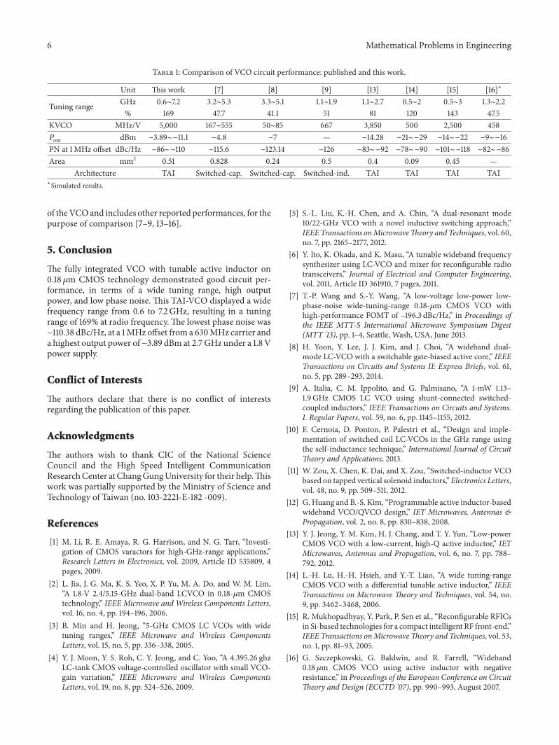