research article enhanced high performance power
TRANSCRIPT

Research ArticleEnhanced High Performance Power Compensation Methodologyby IPFC Using PIGBT-IDVR
Subramanian Arumugom1 and Marimuthu Rajaram2
1AR College of Engineering and Technology Tirunelveli 627423 India2Anna University Chennai 600025 India
Correspondence should be addressed to Subramanian Arumugom sarumugomgmailcom
Received 24 June 2015 Revised 2 September 2015 Accepted 8 October 2015
Academic Editor Wei Yu
Copyright copy 2015 S Arumugom and M Rajaram This is an open access article distributed under the Creative CommonsAttribution License which permits unrestricted use distribution and reproduction in any medium provided the original work isproperly cited
Currently power systems are involuntarily controlled without high speed control and are frequently initiated therefore resultingin a slow process when compared with static electronic devices Among various power interruptions in power supply systemsvoltage dips play a central role in causing disruption The dynamic voltage restorer (DVR) is a process based on voltage controlthat compensates for line transients in the distributed system To overcome these issues and to achieve a higher speed a newmethodology called the Parallel IGBT-Based InterlineDynamicVoltage Restorer (PIGBT-IDVR)method has been proposed whichmainly spotlights the dynamic processing of energy reloads in common dc-linked energy storage with less adaptive transitionTheinterline power flow controller (IPFC) scheme has been employed to manage the power transmission between the lines and therestorer method for controlling the reactive power in the individual lines By employing the proposed methodology the failure ofa distributed system has been avoided and provides better performance than the existing methodologies
1 Introduction
Energy demands are growing remarkably high making itextremely difficult for the power quality to meet energydemand which lead to the load shedding problem and powerquality problem [1] The power quality problem is sensedto be an occurrence of nonstandard voltage current orfrequency [2 3] which is described as the variation in voltagecurrent and frequency in a power system [4ndash6] It alsorefers to a wide variety of electromagnetic phenomena thatcharacterizes voltage and current at a given time and at agiven location in the power system [7ndash9] The power qualityis essential and necessary for proper operation of industrialprocess concerning a good protection to the system for well-being and progress for prolonged usage [10 11] It is clearthat the power quality problems such as voltage sag swellharmonic distortion unbalance transient and flicker canhave a prominent impact on customer devices to result inmalfunctions and loss of production [12]
In modern power systems the use of electronic equip-ment has become widespread This electronic equipment is
more sensitive towards loads and is less tolerant of short-termvoltage disturbances In power quality enrichment functionsthe product of technology-driven custom power and theservice solution are closely related to the equipment devicesAmong the devices of custom power the dynamic voltagerestorer (DVR) [13] is an economical device that plays anadvanced role in a distribution system for reducing thevoltage sag [14]
In remote areas the transmission of load power isnecessary to connect the generation sites with lines whereelectrical power is transmitted through the lines at differentvoltage levels (usually at 230 kV or higher) By increasingtransmission parameters such as capacity and voltage forlong distances the losses during transmission are greatlyreduced Generally multiple paths exist for the flow ofload power in complex interconnected systems Additionallycontrol frequently cannot be initiated due to the slow processtherefore the devices might wear out compared with thedevices in static electronic systems
To reduce these existing difficulties FACTS technol-ogy is employed to handle more services and to improve
Hindawi Publishing Corporatione Scientific World JournalVolume 2015 Article ID 634846 11 pageshttpdxdoiorg1011552015634846
2 The Scientific World Journal
Voltage sag
Injectedvoltage
Restored voltage
SensitiveloadSupply
Energy storage Voltage source inverter
Injectiontransformer
Figure 1 DVR operating principle
the reliability of the system FACTS technology enables theflow of the corresponding load power through the trans-mission lines under both emergency and normal conditionsThe FACTS controller carries the load closer to its thermalrating For further performance improvement in the systemthe static synchronous series compensator (SSSC) has beenextended to the interline power flow controller (IPFC)
Among various power interruptions voltage dips createhigher-level disruption in the power supply systems In publicdistributed systems or in installations faults occur mainlydue to random events and unpredictable voltage dips Byinjecting a voltage at the supply mains of distribution in thetransient line the voltage issues could easily be solved Theoccurrence of voltage deviation could be compensated byinserting the voltage (phase and magnitude) for upstreamdistribution The restorer determines the magnitude andenergy of the voltage that is injected by the DVR [15]The general operating principle of the DVR is schematicallydisplayed in Figure 1
To reload the energy interline DVR (IDVR) providesa dynamic energy storage mechanism in the dc-link [1617] IDVR constitutes load sensitive protection from vari-ous substations for origination of feeder distribution andthereby shares a common dc-link The interline power flowcontroller (IPFC) addresses the common substation issuesof transmission lines [18] The IPFC offers fixed real powertransmission capability between the compensated lines whilethe reactive power in the lines is adjustableThe IDVR schemedelivers real power transfer through the common dc-linksimilar to the IPFC between line loads However the lines areoriginated in IPFC from the substation whereas in the IDVRsystem this happens from various substations The voltagesag imports real power into the IDVR system from the dc-link and the mechanism reloads the energy at a specific levelto maintain the necessary voltage in the dc-link
The Parallel IGBT-Based Interline Dynamic VoltageRestorer (PIGBT-IDVR) has been proposed to provide bet-ter performance in controlling the power flow and powermanagementThe PIGBT-IDVR embraces the Insulated Gate
Bipolar Transistor parallel connection to offer dynamicenergy reloading with a lower transition for energy storage inthe common dc-link The IDVR system serves as a startingpoint for protection of sensitive loads in the distributionfeeders from various substations thereby sharing a commondc-link The interline power flow controller (IPFC) has beensuggested to address the issues related to the transmissionlines and to provide real power capability for direct transferbetween the compensated lines The lines are further man-aged and controlled for reactive power within the system
The rest of this paper has been organized as follows Aliterature review with necessary details on IPFC and IDVRwith the proposed PIGBT method is elaborated in Section 2The proposed work constituting the system design andimplementation has been summarized in Section 3 Section 4elaborates the simulation results of the proposed model withthe necessary discussion Finally the last section shows theconclusions from the research work with a few suggestionstowards future work
2 Related Work
The dynamic voltage restorer (DVR) delivers an economicand technically advanced solution for voltage sag issue [1416] In distribution systems the process of voltage restorationinvolves the injection of real power the topology of the DVRlong duration compensation for voltage sags and storage ofenergy in a dc-link The interline DVR (IDVR) provides adynamically efficient method to reload the energy storage inthe dc-link In power systems various feeders are connectedto share the energy storage Closed-loop load voltage andcurrent-mode control techniques are the two modes ofoperationTherefore the IDVR system provides effectivenessto improve the quality of the power system [19] In real powerflow control mode based on the requirements of the realpower the performance of the voltage restoration will beprocessed There is a clear view of the system mitigation byappearances of lines for long duration for approximately 40of the voltage sag
The interline power flow controller (IPFC) is based onthe Flexible AC Transmission System (FACTS) controller forthe voltage source converter (VSC) and for power flow man-agement among themultiline substation transmission system[20] The power balancing is attained by IPFC through thelines thereby permitting additional power and improving thepower quality By IPFC circuit modeling the transfer of realpower and voltages is improved further [21] As an inverterhas been employed in the dynamic voltage restorer (DVR)the transformer requirement is reduced and consequentlythe switching levels are reduced Ultimately compared withthe DVR topologies the multilevel inverter utilizes fewerswitches and incurs fewer losses at a reduced cost because noinjection is needed for the transformers The switching andcontrol strategies are the compensation strategies for flickersvoltage sags and swells [15] The general circuit descriptionof the IPFC system is outlined in Figure 2
An IGBT-based power stage amplifier provides a validsolution and faster loop-level processing in control systems
The Scientific World Journal 3
Primary(live) side
PFCinductor
L1 D1
Boostdiode
VAC
R1
R2
R3
R4
R5
R6
Rsense
Q1
PWM1H
PFCMOSFET
LIVE_GNDIAC
sense
sense
sense
+HV_BUS
minusHV_BUS
C1
C2
C3
C4
Vdc|VAC|
+
minussim sim
Figure 2 Architectural design of the IPFC system
The corrected values are chosen to drive and influence theblanking times for switching and saturation of semicon-ductors The correction has been supplied directly to thevoltage output of the servo amplifier as a feed forward signalIt consumes substantial power and serves as an alternativeapproach for complex stage power modeling Though thedesign process and the speed of the system are improvedthe associated losses in switching have increased and resultin increased electromagnetic interference making the systembulkier and highly expensive For estimating the voltage inthe sensor drive system the maximum possible accuracy hasbeen found to be limited to the prerequisite value
The FACT device UPFC has been employed for thecontrol of transmission power flow in the system [17 22]With increasing demand for electricity setting up a newline is not easily possible The Flexible AC TransmissionSystem (FACTS) utilizes the existing transmission networkand aUnified Power FlowController (UPFC) using thyristor-controlled devices to emphasize the balancing of voltagepower to control the real and reactive power The controlof the reactive power flow in the dc-link is achieved by theshunt converter and the transmission line and voltage bus ofthe UPFC are controlled by the series convertor The shuntconverter provides reactive power if the bus voltage of theUPFC is constant during the flowof power Both the receivingand sending ends are controlled by the bus voltage
In distributed systems the quality of power is amajor areaof concern due to the connection of sophisticated loads Inthe industrial environment voltage sag results in malfunc-tioning of the equipment To overcome this issue a custompower device is connected with the network to improve thevoltage disturbances in the electrical system [23] To controlthe restorer effectively and dynamically PI controller anddiscrete PWM generator have been employed for effectiveperformance analysis under various fault conditions Use ofthe PI controller and discrete PWM generator reduces thevoltage sags in the DVR [14 19] becomes efficient and fast inthe compensation of the voltage sag and improves the powerquality of the device The power compensation is found tohave achieved approximately 91 with voltage compensationapproximately 44 where an adaptive PI fuzzy controller
has been employed for the compensation process of a voltagerestorer
For voltage stability control and compensation of thereactive power the static synchronous compensator (STAT-COM) has been implemented The STATCOM operates onthe principle of IGBT-based VSC Using the Genetic Algo-rithm (GA) technique the capacitor values of the dc-link andthe source of the battery have been optimized under diverseload conditions An interline power flow controller (IPFC)has been employed to control the power flow in individualtransmission lines among the multiline transmissions TheIPFC transfers the power in a dc-link using two or morevoltage source converters (VSCs) and has the capability ofexchanging reactive power in the transmission system
The deviation in voltage sags results in substantiallosses and disruptions The DVR directly protects voltagesagsswells affecting the sensitive loads on the feeder distri-bution system The DVR injects voltage into the lines andtherebymaintains the optimum value of the voltage loadTheIDVR handles the connection of the restorer with the feederand shares the storage of energy [24] DSTATCOM helps toimprove the quality of power in the distribution systems andthe voltage sag is compensated A neural network method-ology has been implemented to control and achieve theoptimum alleviation of the voltage swell the voltage sags andthe voltage imbalance The multilayer perception in neuralnetworks identifies the dynamic sensitive load voltage andthereby regulates this voltage with lower harmonic distortionand faster response [23] In this paper the proposed modelhas been designed to provide better performance for voltageswell voltage sags and voltage imbalance Moreover themodel consists of parallel combinations of IGBT and IDVRto improve the voltage power and time requirement forprocessing in comparison with the existing methodology
3 The Proposed Scheme
In this section the proposed system is discussed with itsfeatures analysis and design methodology Several changesand losses might occur during power distributionThereforethe distribution of the load is processed dynamically as
4 The Scientific World Journal
Scope 1
Vdc sensed Vdc
1 V
+
+minus
DC Vin2
C3
C1
C4
C7
DAL 2
[A]
[B]
[C]
[D]
[E]
[F]
[G]
[H]
[I]
[J]
[K]
[L]
IGBTAU_1
EC
EC
EC
EC
EC
EC
EC
EC
EC
EC
EC
ECDAU 1
IGBTAM_4DBU 3
IGBTBU_2
IGBTAM_5
IGBTCU_3
DCU 5IGBTAM_6
DBL 4
IGBTCL_10 IGBTCL_11IGBTCL_12
A
B
C
a
b
c
3-phaseV-I measurement 3
1
2
3
Conn 1
Conn 2
Conn 3
Vabc7
Iabc7Scope
IGBTBM_7 IGBTBM_8 IGBTBM_9DCL 5
Figure 3 Proposed PIGBT Simulink model
a time-varying phenomenon in these transmission lines Toovercome the shortcomings of the existing systems in order toreduce transmission time and losses the proposed method-ology has been formulated A distinguished methodologythe Parallel IGBT-Based Interline Dynamic Voltage Restorer(PIGBT-IDVR) has been proposed to achieve power flowcontrol and voltage control for reducing the transmissiontime and switching time for power from one transmissionprocess to another process
Here the functions of the voltage restorer determine therange of compensation and the inductance is assumed to benegligibleThe voltage sags and swells (VSS) function and theinjected voltage are expressed as
VSS =119881119883119899∓ 119881119884119899
119881119883119899
119881119883119899= 119881119884119899∓ 119881119868119899
(1)
The maximum possible magnitude of the output voltageis approximately equal to the dc voltage in the various cells ofa multilevel inverter The maximum possible output voltageis expressed by considering (119899 minus 1)2 cells The derivative ofthe injected voltage and the maximum value of VSS can beexpressed as
119881119868119899=
(119899 minus 1)
2
sdot 119881di
VSSmax =(119899 minus 1)
2
sdot
119881di119881119883119899
(2)
where 119881119883119899
represents the peak value of the load voltage andthe values are potentially equal to a constant value (1 pu)119881
119884119899
represents the peak value of the voltage source119881di represents
the input of the digital voltage and the injected voltage isrepresented by119881
119868119899The level of the output voltage (odd values
that are greater than or equal to 3) is represented as 119899When the modules are connected in parallel the capa-
bility of the current is defined by the parameters that havebeen used by the individual modules Due to the variationof parameters between the various modules the connectionimpedance that is matching may not provide a realistic shar-ing of the current Additionally an unequal device coolingeffect results in a current imbalance within the modules orbetween the modules The temperature during switching isdirectly dependent on the on-state of the respective modulesThe dynamic and static current sharing and the currentimbalance between the parallel connection modules result ina momentous variation in temperature Figure 3 representsthe proposedPIGBTSimulinkmodel and Figure 4 representsthe Simulink model for the proposed PIGBT-based IDVR
The on-state module and current sharing are influencedby various parallel connection resistances Figure 5 showsthe parallel connection module of an on-state linear processcircuit and every individual connection contains a resistorThe on-state process module for a particular probabilityis depicted in Figure 6 The population of median 119881CEsatand deviation are 54V and 0065V respectively and themaximum difference is 265mV An evaluation of the sharingof the module is carried out by grouping the measuredmodule of 2000 into 100 pairs Figure 7 clearly displays thedifferences in probability of 119881CEsat
The voltage difference in the parallel-connected modulesshows clearly that current imbalances occur between themodules To obtain the current imbalance in the modulesan estimate of linear 119881CEsat versus 119868119888 varying between theexpected 13 of the nominal current and the minimal current
The Scientific World Journal 5
A
B
C
A
B
C
A A
B B
C C
a a
ab bbc
c c
VabcIabc
A
B
C
a
bc
A
B
C
a
b
c
A
g
D
SP
B
CA B C
a b c
A
B
C
A
B
C
a
b
c
VabcIabc
V V
V
I
I
I+
+
minus
minus
+
minus
Continuous
Powergui
Conn 1
Conn 2
Conn 3
Con
n 1
Con
n 2
Con
n 3
1 1 1
sim sim sim
1610
3599
1610
3599
Vdc sensed
Subsystem 1
Subsystem 3
PQ
Active and reactivepower
Three-phaseV-I measurement Three-phase
transformer(two windings) 2
Three-phaseV-I measurement 3 V-I measurement 1
V-I measurement 2Three-phase
Three-phase Three-phase V-I measurement 4Three-phase
transformer(two windings) 1
Display 7
Display 2
Dis 2
Ficetingscope 1
Scope 1
Ficetingscope 3
Complex DMagnitude angle 1
Universal B
Vinv_ref
Pulses Uref
Dis 1
PI1
MagPhaseabc
Constant
3-P
Data
T2
Te
ΔΔ
Subsystem 2
minus
Yg
Yg
Figure 4 Proposed PIGBT-IDVR Simulink model
Connectionresistance module 1
Connectionresistance module 2
Itot larr997888997888DC
VT01
VT02
rCE1 IC1
rCE2 IC2
V
Von
+ minus
+ minus
+ minus
Figure 5 Module representing on-state and current sharing
(600A) has been considered At zero amps the on-statethreshold voltage (119881OT) is found to be 25 V
119881CEsat (119868119888) = 119881OT + 119868119888 sdot 119903os (3)
The imbalance of current has to be evaluated because ofvariations in the parallel-connectedmodule which shows thesame drop in voltage assuming connection resistance to bezero The results of the module current have been estimatedon the basis of average 119881CEsat and also on its on-resistance
05
00001
0001
001
01
09
099
0999
09999
Prob
abili
ty
585
58
575
57
565
56
555
55
545
54
535
53
525
52
515
51
5055
495
49
VCEsat 600A 125∘C
+3 s
+2 s
+1 s
Median
minus1 s
minus2 s
minus3 s
Figure 6 On-state process (6500V600A) module
(119903os) The current imbalance in the proposed module isfunctionally evaluated as
119868119888(119899)=
sum
119898
119899=0119881CEsat(119899)2 minus 119881OT(119899)
119903os(119899) (4)
The probability of current imbalance of the parallel-connected module has been obtained as depicted in Figure 8The current imbalance that has been evaluated is found tohave a median of 102 and a maximum of 45
6 The Scientific World JournalPr
obab
ility
0001
001
01
05
09
099
0999
005 01 015 02 025 030
delta_VCEsat
Figure 7 Differences in probability of 119881CEsat
Prob
abili
ty
0999
099
09
05
01
001
0001
0005 001 0015 002 0025 003 0035 004 00450
(Icmax minus Icav)Icav
Figure 8 Current imbalance
By the onoff switching behavior of the inverter the lossesand blanking times have been avoided to the maximumextent It provides a nonlinear process in the power stagesand the switching voltage during emerged time sequences hasbeen processed on the basis of the switching level and the flowof current
The on-time evaluation is necessary in representing thestate and signal of switching from one transmission lineto another The actual times and preceding times of thecarrier signal are found to be triangular in shape as seenfrom Figure 9 Proper sequence of switching should beassigned for attaining minimum current harmonics andcurrent losses Each switch is considered to operate on acomplete cycle (both on and off switching) Figure 10 showsthe inverter state of switching and the cycle begins and endswith the zero vector with the same voltage at all of theterminals Additionally the general flow of switching and on-state current can be understood from the figure below Thecurrentvoltage will be changed even if the state of switchingremains unchanged thus the switches are forced to assumedissimilar states with time
In the parallel connection of modules the connectionderating is based on Safe-Operating-Area (SOA) and thermalderating SOA cares for the current imbalance and theswitching flow It was found that 50of the delay in switching
uavg
avg
wavg
u(t)
(t)
w(t)
0 T
0 T(a) (b) (c) (d)
T
2
Figure 9 General structure of sequence generation
occurs in the off mode Therefore the maximum turn-off inthe process has been reduced in the SOA itself In thermalderating the current sharing in a homogeneous process leadsto higher losses only in the parallel-connected module Thelosses in on-state are expressed with the factor of currentimbalance due to the current mismatch of 5 having 119863 =105
The losses in the switching mismatch in parallel connec-tion operating at the maximum temperature are expressed as
119875ST = (119881OT + 119903CE sdot 119868119888) sdot 119868119888 sdot 119863 (5)
The strategy of the proposed control system circuit hasbeen expressed with its function as per the circuit in Figure 4and the following expressions have been obtained
119868119888= 119862119891
119889119881119894
119889119879
119881119883= 119881119884+ 119881119868
119881119900= 119881119868+ 119903119891119895119891+ 119883119891
119889119895
119891
119889119879
119895119891= 119895119883+ 119895119868
(6)
The expression for injected voltage 119881119868(119878) with the trans-
form function and using the above equations is defined as
119881119868 (119878) =
1
119883119891119868119891119904
2+ 119903119891119868119891119878 + 1
119881119868 (119878)
+
(119903119891+ 119871119891119878)
119883119891119868119891119904
2+ 119883119891119868119891119878 + 1
119862119883
(7)
4 Simulation Study and Performance Analysis
In this section the simulation results of the proposed systemwith necessary analysis have been worked out These evalua-tions are carried out to verify the compensator requirementsof the proposed PIGBT-IDVR system
Figure 11 clearly shows that delay occurs in the processonly if there is any disconnection or if any other issues occur
The Scientific World Journal 7
uload = Ubus uload = 0
T1 T1
T2T2
T1 T1
T2T2
i lt 0
i gt 0
Switching
Switching
(a) (b)
(c) (d)
Figure 10 On-state switching and current flow in power stage
Load
curr
ent
(A)
Time (ms)
tf td
minus15
00
15
Load
vol
tage
(pu)
minus30
0
30
minus30
0
30
(A)
3020100
VSC
curr
ent
Figure 11 Simulation results of VSS with single phase
TheVSC current is almost zero till 20msec After 20msec thecurrent rises correspondingly and rapidly The load voltageshows a linear variation till 20msec but after that particularpoint the linearity becomes disturbed However the loadcurrent shows a linear variation from the beginning until theend
Figure 12 depicts the voltage sag and swells compensationHere 119881
119884(V) is the source voltage of the proposed module
119881119868(V) is the voltage output 119881
119862(V) is the compensated and
injected load voltage and finally 119881119883(V) is the load voltage of
the system The figure clearly shows that the source voltagedrops to a minimum value at the center of the cycle butthe source voltage shows a linear and maximum value at thebeginning and the end of the cycle
The voltage output of the proposed methodology showsa linear variation only after some predetermined value of
VY (V)
VI (V)
VC (V)
VX (V)
minus400minus200
0200400
0120008000400000
minus400minus200
0200400
0120008000400000
minus400minus200
0200400
0120008000400000
minus400minus200
0200400
0120008000400000
Figure 12 VSS compensation
the time Additionally the compensated and injected loadvoltages show a linear variation only after some predeter-mined value of timeThe load voltage of the proposed system
8 The Scientific World Journal
4
2
0
minus2
minus4
V(p
u)
1050
minus05minus1
minus15
I(p
u)
Time (s)
Switch voltage
Switch current
0850845084083508308250820815081080508
Time (s)0850845084083508308250820815081080508
Figure 13 Switching of voltage and current
01 015 02 025005
Time (s)
minus6
minus4
minus2
0
2
4
I AC
(A)
(a) Current through AC system
minus7
minus6
minus5
minus4
minus3
minus2
minus1
0
I d(A
)
004 006 008 01 012 014 016002
Time (s)
(b) Capacitor current at DC side
Time (s)015 0250201005
minus100
minus80
minus60
minus40
minus20
0
20
40
60
80
100
VA
C(V
)
(c) Voltage through AC system
VoltageCurrent
0
20
40
60
80
100
Vt
andI t
(V an
d A
)
004 006 008 01 012 014002
Time (s)
(d) Thyristor voltage and current
Figure 14 Simulation results of VSC single phase with constant voltage source (DC and AC supply)
shows a linear variation from the beginning to the end ofthe cycle clearly indicating that the proposed methodologyproduces a nonfluctuating nonvarying and linear voltageat the output attained mainly by the employment of novelmethods in the proposed systemThis output voltage could beeffectively employed for controlling the system componentsand thus the proposed methodology could be employed forhigh performance and high speed dynamic control systems
The voltage switching and current switching are car-ried out on the basis of the module functionality and theswitching process is depicted in Figure 13 The figure clearlyindicates that the switching of voltage and current happens inan alternativemannerTheperformances are better comparedwith the existing systems
Figure 14 shows the simulation results of VSC with aconstant voltage source of DC and AC supplies Figures 14(a)
The Scientific World Journal 9
Line 2
DC
volta
ge (k
V)
Step inputs
Line 1
000
005
010
015
020
minus5minus4minus3minus2minus10123456
(kVA
)Re
activ
e pow
er
(kW
)Ac
tive p
ower
0200 06 08 1004
Time (s)
0200 06 08 1004
Time (s)
Figure 15 Simulation results of various transmission parameters (double line)
u
w
t22
t12
t12
t02
t22
TT
2
0
t04
t04
(a) Ideal switching
u
w
T
2
T0
t22
t12
t12
t02
t22
t04
t04
T1
T2
T3
T4
T5
T6
(b) Real switching (blanking times)
Figure 16 Switching state and effects of blanking times
and 14(b) show the current flow in an AC system and thecurrent of the capacitor in theVSC respectively AdditionallyFigures 14(c) and 14(d) represent the voltage of the VSC andthe VSC single phase respectively The current flow in theAC system and the current through the capacitor are foundto be linear-valued after some predetermined time valueThe voltages of the VSC show a linear and maximum valuethereby clearly indicating that the proposed methodologycould be used for high speed switching applications Thecorresponding voltage and current transmission in a line arerepresented in Figure 15
Figure 16 shows the effects of the blanking time of theswitching state Correspondingly the derating current output
is shown in Figure 17 The derating current maintains analmost gradual increase as represented by the lowest line inthe graphThe current is also found to be theminimumvalueas desired
Figures 18 and 19 show the current flow and voltage ina line for the proposed methodology The current attains asteady value after only 0015 seconds Initially the currentflow is almost 5 amperes but due to the novel methodologiesemployed in the proposed architecture the current flowis dropped down to minus25 amperes The linearity is furthermaintained till the end of the process in the proposedmethodology
10 The Scientific World Journal
2 times 5SNA 0600G650100 (no derating)2 times 5SNA 0600G650100 (selected)2 times 5SNA 0600G650100 (not selected)2 times 5SNA 0600G650100 (selected)2 times 5SNA 0600G650100 (not selected)
0
1
2
3
4
5
6
7
Der
atin
g (
)
0
200
400
600
800
1000
1200
1400
Curr
ent (
A)
200 400 600 800 1000 12000
Time (s)
Figure 17 Derating current output
Time (s)005004500400350030025002001500100050
minus40
minus35
minus30
minus25
minus20
minus15
minus10
minus5
0
5
I(A
)
Figure 18 Current flow in the line
The power consumption and the magnitude and phase ofthe power are represented in Figures 20 and 21 respectivelyFrom the beginning of the process to 0015 seconds the powercompensation is very low for the proposed methodologyThe power compensation further increases slowlyThe powercompensation sees a steady value only after 0025 secondsThis steady value is further maintained until the end ofthe process clearly indicating that the proposed systemprovides better compensation compared with the existingmethodologies Further in the proposed methodology thecompensation could be attained with proper magnitude andphase value
5 Conclusion and Future Work
In this paper a new methodology called the ParallelIGBT-Based Interline Dynamic Voltage Restorer (PIGBT-IDVR) method has been proposed which mainly targetsthe dynamic processing of energy reloads in common dc-link energy storage with adaptively less transition timeThe operating principles of the proposed methodology havebeen explained clearly The simulation results of the pro-posed module provide better compensation than the existingsystem The evaluation of the proposed methodology hasbeen performed in a common dc-link to provide a faster
600
400
200
0
minus200
minus400
minus600
V(V
)
0 0005 001 0015 002 0025 003 0035 004 0045 005
Time (s)
Figure 19 The voltage in the line
Time (s)
0
1
2
3
4
5
6
7
V(V
)
times106
005004500400350030025002001500100050
Figure 20 Power compensation for output voltage
Time (s)
MagnitudePhase
0
500
1000
1500
2000
2500
3000
3500
4000
4500
Dat
a
005004500400350030025002001500100050
Figure 21 Magnitude and phase of power compensation
process reduction in switching losses dynamic processingof energy reload with less transition in energy storage lesstransmission time and proper management in the flow ofcurrent and voltage The simulated results have been wellevaluated and the performance of the proposed PIGBT-IDVR model has been analyzed to prove the effectiveness ofthe proposedmodel in theMATLABSimulink environmentIn future research the multilevel inverter concept shall beemployed for the power of an electronic systemwithmedium
The Scientific World Journal 11
operating voltage For low frequency operation and with lessdistortion the multilevel concept will be a better alternativemethodology This research work could be extended in thefuture to obtain easy process and better performance
Conflict of Interests
The authors declare that there is no conflict of interestsregarding the publication of this paper
References
[1] E Babaei and M F Kangarlu ldquoVoltage quality improvementby a dynamic voltage restorer based on a direct three-phaseconverter with fictitiousDC linkrdquo IETGeneration Transmissionamp Distribution vol 5 no 8 pp 814ndash823 2011
[2] Y W Li D M Vilathgamuwa F Blaabjerg and P C Loh ldquoArobust control scheme for medium-voltage-level DVR imple-mentationrdquo IEEE Transactions on Industrial Electronics vol 54no 4 pp 2249ndash2261 2007
[3] HMWijekoon DM Vilathgamuwa and S S Choi ldquoInterlinedynamic voltage restorer an economical way to improve inter-line power qualityrdquo IEE Proceedings Generation Transmissionand Distribution vol 150 no 5 pp 513ndash520 2003
[4] G J Li X P Zhang S S Choi T T Lie and Y Z Sun ldquoControlstrategy for dynamic voltage restorers to achieve minimumpower injection without introducing sudden phase shiftrdquo IETGeneration Transmission amp Distribution vol 1 no 5 pp 847ndash853 2007
[5] BWang G Venkataramanan andM Illindala ldquoOperation andcontrol of a dynamic voltage restorer using transformer coupledH-Bridge convertersrdquo IEEE Transactions on Power Electronicsvol 21 no 4 pp 1053ndash1061 2006
[6] F A L Jowder ldquoDesign and analysis of dynamic voltagerestorer for deep voltage sag and harmonic compensationrdquo IETGeneration Transmission amp Distribution vol 3 no 6 pp 547ndash560 2009
[7] A K Jindal A Ghosh and A Joshi ldquoCritical load bus voltagecontrol using DVR under system frequency variationrdquo ElectricPower Systems Research vol 78 no 2 pp 255ndash263 2008
[8] Y W Li P C Loh F Blaabjerg and D M VilathgamuwaldquoInvestigation and improvement of transient response of DVRat medium voltage levelrdquo IEEE Transactions on Industry Appli-cations vol 43 no 5 pp 1309ndash1319 2007
[9] C Fitzer M Barnes and P Green ldquoVoltage sag detectiontechnique for a dynamic voltage restorerrdquo IEEE Transactions onIndustry Applications vol 40 no 1 pp 203ndash212 2004
[10] H K Al-Hadidi A M Gole and D A Jacobson ldquoA novel con-figuration for a cascade inverter-based dynamic voltage restorerwith reduced energy storage requirementsrdquo IEEE Transactionson Power Delivery vol 23 no 2 pp 881ndash888 2008
[11] P Heine and M Lehtonen ldquoVoltage sag distributions caused bypower system faultsrdquo IEEE Transactions on Power Systems vol18 no 4 pp 1367ndash1373 2003
[12] SWWahab andAM Yusof ldquoVoltage sag andmitigation usingdynamic voltage restorer (DVR) systemrdquo Elektrika vol 8 pp32ndash37 2006
[13] I J Balaguer Q Lei S Yang U Supatti and F Z Peng ldquoControlfor grid-connected and intentional islanding operations ofdistributed power generationrdquo IEEE Transactions on IndustrialElectronics vol 58 no 1 pp 147ndash157 2011
[14] S Rahmani A Hamadi N Mendalek and K Al-Haddad ldquoAnew control technique for three-phase shunt hybrid powerfilterrdquo IEEE Transactions on Industrial Electronics vol 56 no8 pp 2904ndash2915 2009
[15] H Jou K-D Wu J-C Wu C-H Li and M-S Huang ldquoNovelpower converter topology for three-phase four-wire hybridpower filterrdquo IET Power Electronics vol 1 no 1 article 164 2008
[16] R J Majumder ldquoReactive power compensation in single-phase operation of microgridrdquo IEEE Transactions on IndustrialElectronics vol 60 no 4 pp 1403ndash1416 2013
[17] C Attaianese and G Tomasso ldquoPredictive compensation ofdead-time effects in VSI feeding induction motorsrdquo IEEETransactions on Industry Applications vol 37 no 3 pp 856ndash8632001
[18] S YangQ Lei F Z Peng andZQian ldquoA robust control schemefor grid-connected voltage-source invertersrdquo IEEE Transactionson Industrial Electronics vol 58 no 1 pp 202ndash212 2011
[19] J-L Lin ldquoA new approach of dead-time compensation forPWM voltage invertersrdquo IEEE Transactions on Circuits andSystems I Fundamental Theory and Applications vol 49 no 4pp 476ndash483 2002
[20] W Tangtheerajaroonwong T Hatada K Wada and H AkagildquoDesign and performance of a transformerless shunt hybridfilter integrated into a three-phase diode rectifierrdquo IEEE Trans-actions on Power Electronics vol 22 no 5 pp 1882ndash1889 2007
[21] A Vaccaro G Velotto and A F Zobaa ldquoA decentralized andcooperative architecture for optimal voltage regulation in smartgridsrdquo IEEE Transactions on Industrial Electronics vol 58 no10 pp 4593ndash4602 2011
[22] J M Guerrero J Matas L G de Vicuna M Castilla andJ Miret ldquoDecentralized control for parallel operation of dis-tributed generation inverters using resistive output impedancerdquoIEEE Transactions on Industrial Electronics vol 54 no 2 pp994ndash1004 2007
[23] T Sauter and M Lobashov ldquoEnd-to-end communicationarchitecture for smart gridsrdquo IEEE Transactions on IndustrialElectronics vol 58 no 4 pp 1218ndash1228 2011
[24] NYDaiMCWong andYDHan ldquoThree-dimensional spacevector modulation with DC voltage variation control in a three-leg centre-split power quality compensatorrdquo IEE ProceedingsElectric Power Applications vol 151 no 2 pp 198ndash204 2004
TribologyAdvances in
Hindawi Publishing Corporationhttpwwwhindawicom Volume 2014
International Journal of
AerospaceEngineeringHindawi Publishing Corporationhttpwwwhindawicom Volume 2014
FuelsJournal of
Hindawi Publishing Corporationhttpwwwhindawicom Volume 2014
Journal ofPetroleum Engineering
Hindawi Publishing Corporationhttpwwwhindawicom Volume 2014
Industrial EngineeringJournal of
Hindawi Publishing Corporationhttpwwwhindawicom Volume 2014
Power ElectronicsHindawi Publishing Corporationhttpwwwhindawicom Volume 2014
Advances in
CombustionJournal of
Hindawi Publishing Corporationhttpwwwhindawicom Volume 2014
Journal of
Hindawi Publishing Corporationhttpwwwhindawicom Volume 2014
Renewable Energy
Submit your manuscripts athttpwwwhindawicom
Hindawi Publishing Corporationhttpwwwhindawicom Volume 2014
StructuresJournal of
International Journal of
RotatingMachinery
Hindawi Publishing Corporationhttpwwwhindawicom Volume 2014
EnergyJournal of
Hindawi Publishing Corporationhttpwwwhindawicom Volume 2014
Hindawi Publishing Corporation httpwwwhindawicom
Journal ofEngineeringVolume 2014
Hindawi Publishing Corporation httpwwwhindawicom Volume 2014
International Journal ofPhotoenergy
Hindawi Publishing Corporationhttpwwwhindawicom Volume 2014
Nuclear InstallationsScience and Technology of
Hindawi Publishing Corporationhttpwwwhindawicom Volume 2014
Solar EnergyJournal of
Hindawi Publishing Corporationhttpwwwhindawicom Volume 2014
Wind EnergyJournal of
Hindawi Publishing Corporationhttpwwwhindawicom Volume 2014
Nuclear EnergyInternational Journal of
Hindawi Publishing Corporationhttpwwwhindawicom Volume 2014
High Energy PhysicsAdvances in
The Scientific World JournalHindawi Publishing Corporation httpwwwhindawicom Volume 2014
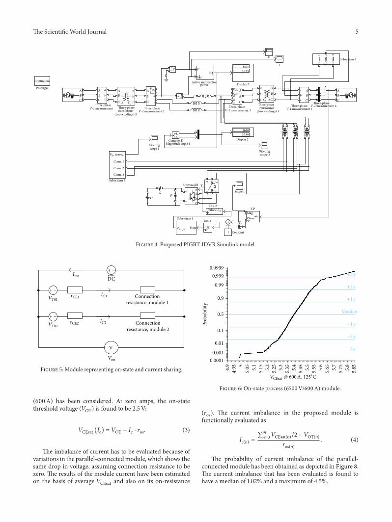
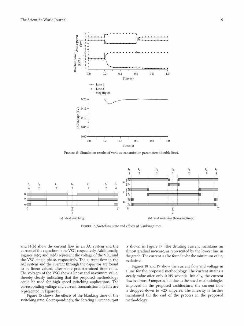