resistance and resistivityee.sc.edu/personal/faculty/simin/elct563/02 semiconductors i... ·...
TRANSCRIPT
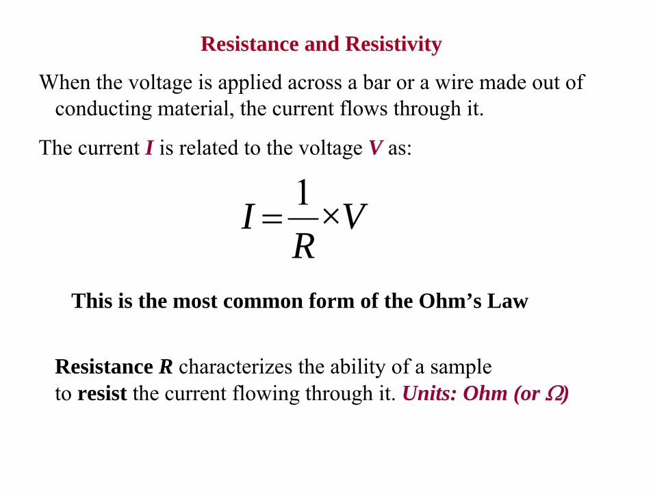
Resistance and Resistivity
When the voltage is applied across a bar or a wire made out of conducting material, the current flows through it.
The current I is related to the voltage V as:
This is the most common form of the Ohm’s Law
1I ×VR
=
Resistance R characterizes the ability of a sample to resist the current flowing through it. Units: Ohm (or Ω)

Resistance and resistivity
The higher is the resistance R the lower is the current at a given voltage.
A and L describe the geometry of a sample or a wire.
The larger is the cross-section A the smaller is R, the higher is the current.
The longer is the length L, the higher is R, the smaller is the current;
ALR ρ= ρ is the resistivity of the material. Units: Ohm*m
ρ describes the electrical properties of the material itself, independent of the shape of the bar or wore.
The higher is ρ, the higher is R and the lower is the current
LRA
ρ=
1I ×VR
=

Ohm’s Law using conductance and conductivity.
AGL
σ=
G and R are related simply asG = 1/R
σ and ρ are related simply asσ = 1/ρ
σ is the conductivity of the material. Units: Siemens/m or S/mσ describes the electrical properties of the material itself, independent of the shape of the bar or wore.
The higher is σ, the higher is G and the higher is the current
I = G × VThis is just another form of the same Ohm’s lawG is the conductance of a bar or a wire. Units: Siemens or S

Mobile charges concentration and mobility
Material parameters that determine the conductivity are 1) mobile charge concentration, n and2) mobile charge mobility, µ
σ = q n µCorrespondingly, ρ = 1/(q n µ)
The difference in electrical conductivity (or resistivity) between different materials arises from different n and µ

The Origin of Electric Conductance
• Free electrons can freely move along the crystal (colliding with the atoms)
• Their kinetic energy comes from the lattice vibrations
• In equilibrium, free electrons move randomly inside the crystal.• In electric field, free electrons drift toward positive electrode creating
electric current
Semiconductor materials

Conductors, Insulators and Semiconductors
µσ nq=
Metal:~ 1023 atoms per 1 cm3
Every atom donates 1 free electron: n ~ 1023 cm-3
Insulator:~ 1023 atoms per 1 cm3;
No free electrons:
n ~ 0
Semiconductor:~ 1023 atoms per 1 cm3;
Some atoms donate free electrons n ~ 1010 - 1019 cm-3
The mobility in different materials differs around 1000 times.
The concentration of free electrons n in different materials differs
around 1023 times!
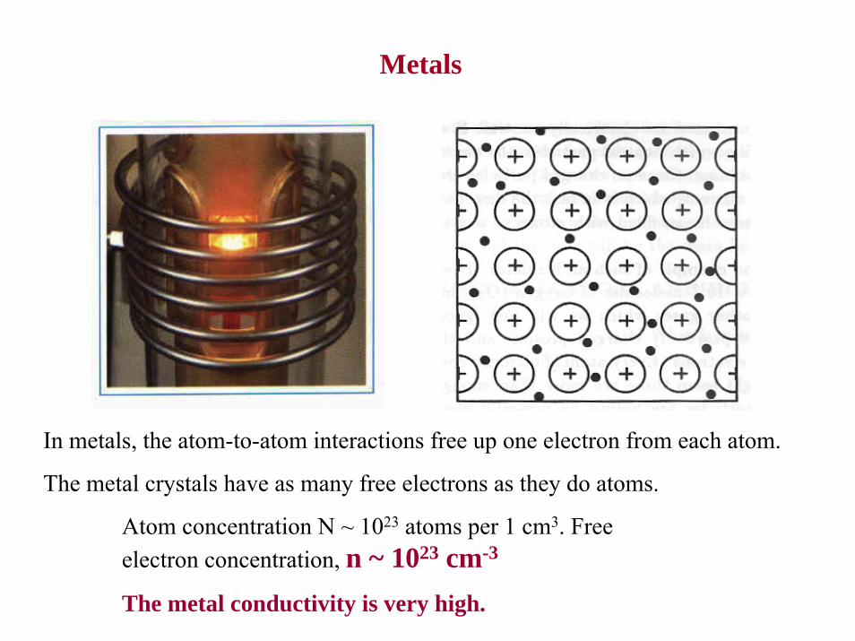
Metals
In metals, the atom-to-atom interactions free up one electron from each atom.
The metal crystals have as many free electrons as they do atoms.
Atom concentration N ~ 1023 atoms per 1 cm3. Free electron concentration, n ~ 1023 cm-3
The metal conductivity is very high.

Si crystal lattice structure, showing the valence electrons associated with each bond.
Note that each silicon atom now has eight valence electrons in the neighborhood,
but that they are all shared, two with each of its four neighbors.No free electrons!
Silicon crystal
Silicon (Si) is the most important semiconductor material

The photons – elementary particles of light can break the bonds and create free electrons in the Si crystal
Silicon crystal under illumination

Silicon crystal at elevated temperature
If the temperature is high enough the crystal lattice vibrates and delivers extra energy to electrons
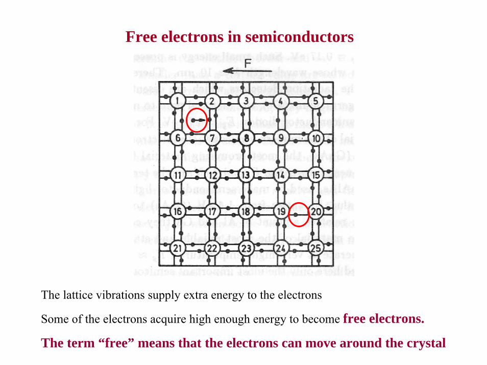
The lattice vibrations supply extra energy to the electrons
Some of the electrons acquire high enough energy to become free electrons.
The term “free” means that the electrons can move around the crystal
Free electrons in semiconductors

Free electron concentration in semiconductors
• The probability for an electron to acquire the energy high enough to break the atomic bonds is very low
• This probability is a very strong function of the temperature (at higher temperatures the lattice vibrations are stronger)
kTEG
eNn 20
∆−
×=
The energy required to produce a free electron in a crystal is called
the bandgap energy, ∆EGIn the metals, the bandgap energy is equal to zero.In dielectrics, the bandgap energy is much higher than in semiconductors.
k = 1.38 × 10⁻²³ J/K, is the Boltzmann constant, T is the crystal temperature, in Kelvin (K)N0 ≈ 2×1019 cm-3 for most semiconductor materials

kTEG
eNn 20
∆−
×=The energy unit used in micro-world - Electron-Volt:
1 eV = 1.6 ×10⁻¹⁹ J
Using the eV-units,
k × T ≈ 4 × 10-21 J ≈ 0.026 eV (at room temperature, T ≈300 K)
In most semiconductors,
EG ≈ (2…10)× 10-19 J = 1 – 3 eV;
In Si, EG = 1.1 eV.
Note, kT << ∆ EG.
Electron - Volt

kTEG
eNn 20
∆−
×=for Si,
N0 ≈ 2×1019 cm-3
At room temperature: kT0 = 0.026 eV;∆EG = 1.1 eV
Free electron concentration in Silicon
∆EG/(2×kT) = 21.15; e -21.15 = 6.5× 10⁻¹⁰
n20C = 1.3×1010 cm-3
At 100 oC: kT = kT0×(397K/300K) = 0.026 × 1.323 eV = 0.034 eV;
n100C = 1.9×1012 cm-3; n is much smaller than the Si atom concentration NSi y1023 cm-3

kTEG
eNn 20
∆−
×=
Free electron concentration in Silicon
n(t) for Si
0.00E+00
5.00E+13
1.00E+14
1.50E+14
2.00E+14
2.50E+14
3.00E+14
3.50E+14
4.00E+14
4.50E+14
0 100 200 300 400
t, oC
n, c
m-3

When the electron leaves the Si atom, the latter is lacking one electron.
The bonds lacking an electron behave as free POSITIVE charges: holes
In electric field, the hole “moves” toward negative electrode
Electrons and Holes in Semiconductors

Electrons and Holes in Semiconductors
• The 'hole' is an abstraction; it has no substance and does not actually move itself, but movement of electrons in the opposite direction is perceived as the hole moving.
• In an ideal (intrinsic) semiconductor crystal, ni = pi
• Hole mobility is usually lower than electron mobility.
EG
Electrons have negative charge and move toward positive electrode;
Holes have positive charge and ”move” toward negative electrode
Any electron that leaves the atom creates a “hole” in the valence orbit.
In pure (also called intrinsic) Si, free electrons and holes appear in PAIRS
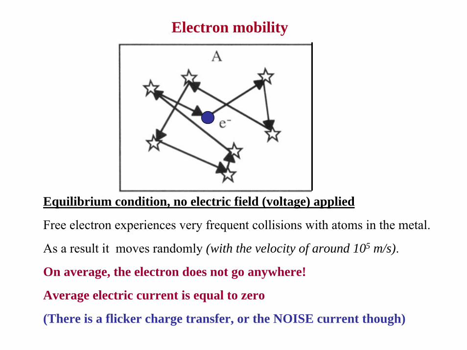
Electron mobility
Equilibrium condition, no electric field (voltage) applied
Free electron experiences very frequent collisions with atoms in the metal.
As a result it moves randomly (with the velocity of around 105 m/s).
On average, the electron does not go anywhere!
Average electric current is equal to zero
(There is a flicker charge transfer, or the NOISE current though)
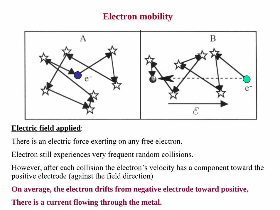
Electric field applied:
There is an electric force exerting on any free electron.
Electron still experiences very frequent random collisions.
However, after each collision the electron’s velocity has a component toward the positive electrode (against the field direction)
On average, the electron drifts from negative electrode toward positive.
There is a current flowing through the metal.
Electron mobility
Electron mobility
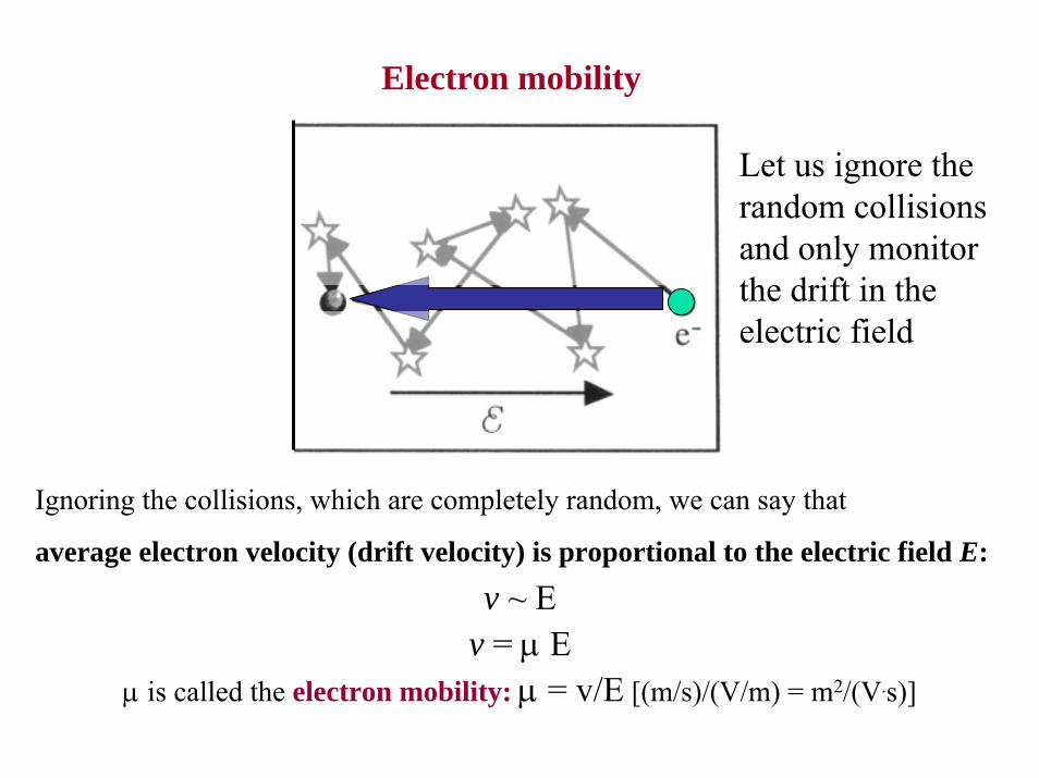
Ignoring the collisions, which are completely random, we can say that
average electron velocity (drift velocity) is proportional to the electric field E:
v ~ Ev = µ E
µ is called the electron mobility: µ = v/E [(m/s)/(V/m) = m2/(V.s)]
Let us ignore the random collisions and only monitor the drift in the electric field

Electron mobility example
The electron mobility in silicon (Si) is 1000 cm2/(V-s).
What is the electron drift velocity if the voltage across the sample is 5V and the sample is d =1 mm thick?
Solution. Assuming uniform electric field in the sample, the electric field and the voltage are related as: E = V/d, where d is the distance between the electrodes.
E = V/d = 5V/10-3 m = 5.103 V/m
vdr = µ E; µ = 1000 cm2/(V-s) = 1000 × 10-4 m2/(V-s) = 0.1 m2/(V-s).
vdr = 0.1 m2/(V-s) × 5.103V/m = 500 m/s
Compare this to the electron “thermal” velocity: vT ≈ 105 m/s >> vdr

How much would be the resistance of the (1 cm×1cm× 1cm) Si sample?The electron mobility in Si, µ = 1000 cm2/(V ×s).Consider room temperature:
Resistance of Silicon sample
n = 1.3×1010 cm-3
µ = 1000 cm2/(V ×s)q = 1.6 ×10⁻¹⁹ C
σ = 1.6 ×10-19 C × 1.3×1010 cm-3 × 1000 cm2/(V ×s)
σ = 2.08 × 10⁻⁶ (Ohm × cm)-1
AL
ALR
qn
×==
=
σρ
µσ1
;
ρ = 4.8 × 10⁵ Ohm × cm
R = 4.8 × 10⁵ Ohm × cm ×1 cm /(1cm ×1cm) = 4.8 × 10⁵ Ohm
The resistance is too high for most practical purposes.
Due to very low intrinsic electron and hole concentrations, ideal (intrinsic) found very limited applications in electronics.
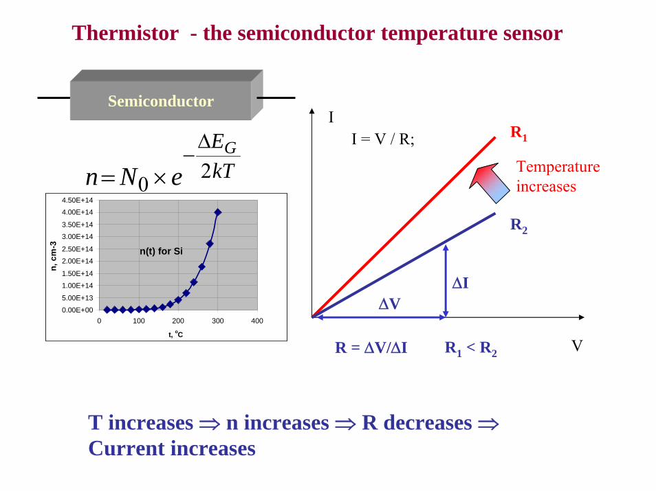
Thermistor - the semiconductor temperature sensor
I = V / R;
R = ∆V/∆I R1 < R2 V
IR1
R2
∆V∆I
T increases ⇒ n increases ⇒ R decreases ⇒Current increases
Semiconductor
kTEG
eNn 20
∆−
×=
n(t) for Si
0.00E+00
5.00E+13
1.00E+14
1.50E+14
2.00E+142.50E+14
3.00E+143.50E+14
4.00E+144.50E+14
0 100 200 300 400
t, oC
n, c
m-3
Temperatureincreases

Thermistor as a solid-state switch:Effect of self-heating on semiconductor thermistor
Initially, the thermistor temperature = room temperature
When the voltage is applied, the current flows through the thermistor: I = V/R;
The Joule heat increases the device temperature T
The current generates the Joule heat: P = V ×I = I2 R
At higher temperature the thermistor resistance R decreases
As R decreases, the current through the device increases

Thermistor as a solid-state switch:Effect of self-heating on semiconductor thermistor
As I increases, the power, i.e. the Joule heat further increases as P = V ×I = I2 R
The device temperature T increases even more
The device resistance decreases further
The device current further increases

V
I
Effect of self-heating on semiconductor thermistor
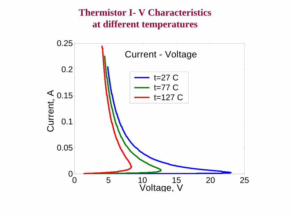
0 5 10 15 20 250
0.05
0.1
0.15
0.2
0.25Current - Voltage
Voltage, V
Cur
rent
, A
t=27 C t=77 C t=127 C
Thermistor I- V Characteristics at different temperatures

Photoconductors
Under the illumination, the concentration of electron and hole pairs consists of the equilibrium
(dark) concentration and that of the photoexcited carriers:
n = n0 + nph; p = p0 + pph;
Correspondingly, the current has two components:
I = ID + Iph
ID – the “dark” current; IPh – the “photo” current
The current through the sample is

Photoresistor - the semiconductor light sensor
I = V / R;
R = ∆V/∆I R1 < R2 V
IR1
R2
∆V∆I
Light intensity increases ⇒ n increases ⇒ R decreases ⇒Current increases
Semiconductor
Light intensityincreases