review and analysis of the impacts and effects on low ... on low power vlsi circuits operating in...
TRANSCRIPT

Review and Analysis of the Impacts and Effects on Low Power VLSI Circuits Operating in Subthreshold Regime
D. Jennifer Judy1, V. S. Kanchana Bhaaskaran2 1,2School of Electronics Engineering, VIT University, Chennai-600127, Tamil Nadu, India
1jennisteef @ yahoo.co.in 2vskanchana @ gmail.com
Abstract − In ultra low power portable devices set towards realizing a long battery life, low energy consumption per operation is the primary design constraint. Hence, operating the circuits in weak inversion or the sub-threshold region, with the subthreshold leakage current acting as the primary computing current, turn out to be a promising solution. Though such a methodology limits the performance in terms of speed, it exhibits a lot of benefits in terms of reduced dynamic power and leakage power, added with high transconductance gain. In the subthreshold regime, the high sensitivity of the devices to the process, voltage and temperature (PVT) variations prove to be a major challenge to be tackled, due to the exponential dependence of drain current on the threshold voltage VT. In this paper, the operational behaviours of VLSI circuits, while operating in the weak inversion region are illustrated with explicit simulation results, waveforms and discussions. Moreover, the lack of robustness of the device in the subthreshold regime is also analyzed. The elimination of the PVT variability issues by employing body biasing strategies is explored. Each of these analyses use precisely exemplified simulation methodologies. The results and discussions are depicted through ample simulation results. The impact of technology scaling on VLSI circuits in the subthreshold regime is explored. Minimum energy point, optimum Vdd and optimum VT are also evaluated. It is followed by the channel upsizing, which is considered to be the most potential circuit level technique for addressing most of the issues in the subthreshold regime. The entire analyses and study are done with the use of a 16-bit CLA adder as the benchmark circuit. PTM (Predictive Technology Models) models of 32nm, 45nm, 65nm, 90nm, 130nm and 180nm have been used in the simulations using the industry standard EDA tool.
Keywords− Subthreshold regime; DIBL; Subthreshold swing; Body Biasing; Channel upsizing
I. INTRODUCTION Portability is the trend in the electronics market. The emerging portable devices such as the hearing aids,
pacemakers, defibrillators and implantable devices demand a long battery lifetime as a primary design parameter to be considered. Higher power consumption and high on-chip temperature in such devices may lead to a shorter battery life, leading to the batteries necessitating frequent replacement. Hence, in such applications, the power reduction is of paramount importance rather than the speed performance. These applications are ideal candidates for sub-threshold operation of devices. The subthreshold circuits operate in weak inversion region, with the power supply voltage Vdd < Vth, where Vdd and Vth are the supply and the threshold voltages respectively. The scaled down supply voltage leads to a higher energy efficiency, though it limits the speed. The reduced power consumption makes the circuits lighter, reduces or eliminates the heavier cooling subsystems, and extends the life period of the power source. Such circuits in the weak inversion region are capable of operating at a frequency of few MHz. However, it may be noted that the scaled down MOSFET is capable of switching at GHz ranges. Thus, it may pointed out that rather than overdesigning the circuits for higher speeds resulting in increased power dissipation, the devices as well may be operated in lower speed, thus trading off between the power and speed. Additionally, the subthreshold operation as discussed above can use lower supply voltage that is below Vth resulting in further reduction of power. Note that the subthreshold leakage current is used as the computation current [1] [2] [3].
The literature have identified that the subthreshold circuits can be applied to applications that incur burst mode of operation. In other words, such circuits are active for a short time TACTIVE and remain idle for the remaining longer TIDLE [3]. In such cases, rather than operating the circuits in the strong inversion region resulting in wasted power; they can be run in the subthreshold regime with much lower frequency ranges. Fig. 1 depicts a transient involving three operations during each clock cycle, carried by super and subthreshold circuits. Here, the subthreshold frequency is given by 1/T SUBTHRESHOLD [3].
D. Jennifer Judy et.al / International Journal of Engineering and Technology (IJET)
ISSN : 0975-4024 Vol 5 No 5 Oct-Nov 2013 3870

Fig. 1 Super threshold and Subthreshold operation
Hence, the sub-threshold design approaches are suitable for a wide class of low power or low energy applications, which demand a detailed study and investigation. This paper is organized as follows: Section II gives an insight to the varied features (notions) in operating the MOSFETs in the circuits in weak inversion region. Section III discusses the device sizing principles. Section IV reports the various beneficial effects of the circuit configured in the subthreshold regime of operation. Section V identifies the advantages brought about by the technology scaling even while operating in the subthreshold region. Sections VI and VII detail the PVT variability issues and body biasing techniques for addressing those issues. Section VIII analyses the simulation of benchmark circuits in weak inversion region. Section IX presents the channel upsizing method as the vital solution for most of the issues faced by the subthreshold operation. Section X concludes with a glimpse into the possible scope of continued research.
II. SUBTHRESHOLD OPERATION OF THE ULTRA LOW POWER VLSI CIRCUITS Operation of the circuits in the region, where Vdd is less than the threshold voltage VT is the subthreshold
operation of the circuits. When Vgs < Vth, the MOSFET is OFF as the inversion layer is yet to be formed and hence, will not support conduction of current. However, in this weak inversion region, there is diffusion of minority carriers between the drain and the source contributing the subthreshold leakage current. This subthreshold leakage current is the operating current of the device. The I-V and the C-V behavior in the subthreshold region are shown in Fig. 2 and Fig. 3. They are very different from the behavior in the strong inversion or super threshold region. In the subthreshold region, the exponential behavior of the current ID versus Vgs is illustrated in Fig. 2. with a 65nm BPTM (Berkeley Predictive Technology) Model operated by Vdd at 0.3 V and Vgs varying between 0.3V and 0.7V. The operating features are as follows:
• Due to the exponential dependence, the transconductance gm= Δ Ids /Δ Vgs of the device is high thus increasing the gain of the circuit.
• The quadratic dependence of the dynamic power dissipation on Vdd would greatly improve the power efficiency achieved due to the scaled down power supply voltage.
• The leakage current components such as gate induced drain leakage (GIDL), reverse biased PN junction leakage and the gate tunneling current are negligible owing to their dependence on Vdd in the subthreshold regime. These aspects are explored in Section IV.
Fig. 2. Exponential dependence of the drain current on the VGS (ID vs Vgs plot)
T A C T IV E T ID L E
T S U B T H R E S H O L D
D. Jennifer Judy et.al / International Journal of Engineering and Technology (IJET)
ISSN : 0975-4024 Vol 5 No 5 Oct-Nov 2013 3871

Fig. 3. Gate capacitance vs. Gate Voltage (CG vs Vgs plot)
In a long channel device, the threshold voltage is independent of the drain bias and the channel length. However, in deep sub-micron technologies (DSM), the source and the drain depletion regions penetrate considerably into the channel and control the potential and hence, the field inside the channel. Hence, the threshold voltage and the subthreshold current of short-channel devices vary with the drain bias. This effect is referred to as (Drain Induced Barrier Lowering) DIBL and is defined by the parameter DIBL coefficient η. The subthreshold leakage current equated to the total current in the weak inversion region, and taking into account the DIBL factor, is given by eqn. (1).
µ exp – 1 (1)
where weff is the effective width of the device, Leff is the effective channel length, Ncheff is the effective channel doping, µ is the carrier mobility, si is the dielectric constant of the semiconductor, s is the surface potential, m is the body effect coefficient related to the subthreshold swing, Vgs is the gate voltage, Vds is the drain voltage and vT is the thermal voltage given by kT=q, k is the Boltzmann constant, T is the temperature, and q is the electronic charge [4].
Further, the process variations (PV) pose severe consequences on the operation of the subthreshold circuits as discussed below. The process variations cause fluctuations in the threshold voltage that have an exponential effect on the current. Thus, the threshold voltage being one of the most susceptible parameters to process variations is directly affected by the variability factors such as 1) random dopant fluctuation 2) variation in the oxide thickness and 3) variation in channel length for highly scaled devices. All these process variations are generally prevalent and thus the subthreshold circuits suffer from increased sensitivity to these variations. Hence, innovative design techniques need to be employed to counter these effects. The techniques are explained in detail in section VII.
In addition, another effect in the subthreshold region of operation is the reduced gate capacitance. An incremental change in the gate charge leads to an increased series depletion capacitance and the total gate capacitance Ci of a device is given by, = , Cd ∥ ∥ ∥ (2) where Cox, Cd are the oxide and depletion capacitances respectively. While Cif and Cof are the fringe capacitances, Cdo is the overlap capacitance [5]. The distribution of various capacitive components is shown in Fig. 4.
Fig.4. Different capacitive components of a MOSFET
D. Jennifer Judy et.al / International Journal of Engineering and Technology (IJET)
ISSN : 0975-4024 Vol 5 No 5 Oct-Nov 2013 3872

Equation 2 shows that the gate capacitance in the subthreshold region is less than that garnered in the super threshold region. This is due to the reason that the series depletion capacitance does not play a part in the strong inversion region. This results in reduction of the gate capacitance in the subthreshold region.
. Fig. 5. Ioff Deteriorating due to the DIBL effect
Fig. 6. Ion/Ioff ratio in the subthreshold region
Moreover, in contrast to the strong inversion region, where Ids saturates only when Vds >Vgs – Vth, the drain current in the subthreshold regime saturates and becomes independent of Vds even while Vds >3kT/q (~78mV at 300K) itself.
Hence, the long channel devices are good current sources in the subthreshold region in the operating voltage range of 3kT/q to Vdd. This current source property enables better pass gate logic or in other words reduces the voltage degradation in series connected devices in the subthreshold region. This is due to the fact that the voltage drop across the devices is just the 3kT/q drop (~78 mV) as against the full Vth value of around 700mV.
Figure 5 shows the super threshold or nominal current, IOFF, nom and subthreshold current IO, sub, when simulated in the technology nodes of 45nm, 65nm, 90nm, 130nm and 180nm PTM models. The power supply and gate voltage levels applied in the nominal mode and subthreshold mode are 0.3V and 1.1V respectively in the 45nm technology node. Similarly, for the other technology nodes their respective nominal voltage and 0.3V are applied when operated in the strong and weak inversion region. As can be observed, the leakage current Ioff in the subthreshold logic has increased due to the DIBL effect. It is shown comparable to the current in the active state Ion . Hence, the ratio Ion/ Ioff is deteriorating in the subthreshold region than the strong inversion as illustrated in Fig. 6. However it can be alleviated with channel upsizing as explained in section IX.
Another parameter that needs attention in the subthreshold region is the subthreshold swing represented by the subthreshold slope factor S .It can be defined as the amount of the gate voltage needed to change the drain current by a decade and is determined as follows.
10 1 1 10 (3)
D. Jennifer Judy et.al / International Journal of Engineering and Technology (IJET)
ISSN : 0975-4024 Vol 5 No 5 Oct-Nov 2013 3873

Equation (3) shows that the subthreshold swing is dependent on the substrate doping and the oxide thickness and any variability in these parameters may degrade the subthreshold swing S. However, increasing the channel length will increase the Beta ratio β and give better subthreshold slope due to the less reverse short channel effects (RSCE). The variation of S and η over the technology nodes is presented in Fig. 7.
Fig. 7. Subthreshold swing S and DIBL coefficient η over the technology nodes
III. DEVICE SIZING FOR OPERATION IN THE WEAK INVERSION REGION: A typical CMOS combinational circuit with pull-up PMOS devices and pull-down NMOS devices has been
considered for operation in weak inversion region. The devices are sized in such a way that the strengths of the pull up network (PUN) comprising of the PMOS devices and the pull down network (PDN) formed by the NMOS devices are equal. The rise time tplh and fall times tphl of the devices are dependent on the strengths of the PUN and PDN respectively and hence are equal. The ratio of the width of the PMOS device to that of the NMOS device in a CMOS inverter is called the Beta ratio β and is the main sizing parameter in the subthreshold regime (β=WP/WN ). The strength of the device can be tuned by the following values:
• W/L ratio or Beta ratio β • Selecting the zero bias threshold voltage Vtho for the adopted technology • By statically or dynamically tuning the bulk bias
For strong inversion region, β takes the value 2.5 for equal currents in the PMOS and NMOS devices. This value of Beta ratio is due to the fact that the mobilities of the electrons and the holes are also in the same ratio. However in the subthreshold regime, besides the difference in their mobilities, the discrepancies in the threshold voltage and the subthreshold swing of the PMOS and NMOS devices also play a role in device sizing. This is attributable to the exponential dependence of current in the devices on Vth. Hence, devices for the subthreshold CMOS circuits have to be sized accordingly [6]. For example, in this paper, for the 45nm technology node, the worst case corner models SF (SLOW/FAST) and FS (FAST/SLOW) are operated at varied supply voltages and at different values of aspect ratios. The point of intersection of these worst case curves i.e., Wp =135nm; Wn=65nm, is the optimum value of aspect ratio for the 45nm technology node in the subthreshold regime.
IV. BENEFICIAL NATURE OF OPERATION IN SUBTHRESHOLD REGIME In this section, the beneficial effects of the subthreshold logic are observed through simulation of an 8-bit
CLA adder employed as a benchmark circuit. A. Dynamic Energy dissipation:
The total energy dissipation of a circuit is the sum of the dynamic energy due to switching in the nodal capacitances and the static energy due to the leakage current flowing through the devices [6]. The total energy per operation can expressed as
(4)
D. Jennifer Judy et.al / International Journal of Engineering and Technology (IJET)
ISSN : 0975-4024 Vol 5 No 5 Oct-Nov 2013 3874

where Nsw is the number of switched nodes to perform the operation, Ileak is the total circuit leakage current, Wmin is the minimum device width, CL is the load capacitance per unit width and LD the logic depth.
Fig. 8. Simulated results of the dynamic power dissipation of an 8 bit CLA adder in the subthreshold regime for the various technology
nodes and for different supply voltage Vdd
The simulation results of the benchmark circuit depicting the dynamic power are plotted in Fig. 8. As can be expected, the capacitance per unit width CL and the device minimum width Wmin are reducing in tune with technology scaling. This factor results in reduced dynamic power dissipation Edyn as predicted by Eqn (4). Further, it can be observed that the quadratic dependence of Edyn on Vdd mainly contributes to the substantial reduction of dynamic power dissipation [4] while operating in subthreshold regime.
B. Static power dissipation and leakage currents in the weak inversion region:
Fig. 9. Static power dissipation of 8 bit CLA adder in subthreshold regime for 45nm, 65nm, 90nm and 130nm technology nodes for varying
Vdd
The static power dissipation Estat decreases exponentially with increasing Vdd in the subthreshold regime as in Eqn (5). As the supply power (VDD) is reduced for subthreshold operation, the static power is also reduced as shown in Fig. 9. Further, the static power is dependent on the leakage current Ileak of the subthreshold region as given below.
10 (5)
The leakage current (ILeak) comprises various components, the main contributor being the subthreshold current. The subthreshold leakage current in a short-channel device varies with the drain bias due to the DIBL effect. With the drain voltage applied to a short channel device, the depletion regions of the drain extend further and interact with the source near the channel surface. This lowers the source potential barrier, resulting in a decrease of the threshold voltage. Thus, some of the carriers from the source may overcome the reduced potential barrier and reach into the channel surface independent of gate voltage.
This DIBL effect is enhanced at high drain voltages and shorter channel lengths. With a reduced supply voltage during the subthreshold operation, VDS is much lower than during strong-inversion operation, and hence, DIBL is highly reduced. Subthreshold leakage due to DIBL reduces by 2 to 10 times depending on the technology chosen and VDD scaling. Therefore, subthreshold leakage power is reduced by 4X to 90X, in comparison with strong inversion circuits.
D. Jennifer Judy et.al / International Journal of Engineering and Technology (IJET)
ISSN : 0975-4024 Vol 5 No 5 Oct-Nov 2013 3875

Gate tunneling current, which happens to be the major leakage current in deep sub-micron technologies, depends on the voltage across the gate. Hence, it is justified that the gate tunneling current has decreased due to the scaling of Vdd and becomes almost negligible in the subthreshold operation [7] [8] as depicted in Fig. 9.
GIDL (Gate induced drain leakage) current becomes significant when a high VDS is applied along with a low VGS. It is reasoned that the GIDL is negligible due to the reduced VDS in the subthreshold circuits. The reverse-bias diode leakage is also drastically reduced with the decreased supply voltage in the subthreshold region of operation. Thus, the leakage power scales down linearly with Vdd , lowering Estatic, as depicted in Fig. 9. C. Minimum energy point, Optimum Power Supply Voltage Vddopt and Optimum Threshold Voltage VTopt for
Subthreshold Operation:
Fig. 10. Minimum energy point shift with variability in LG in VT
Fig. 11. MEP point &Vddopt for technology nodes 45nm, 65nm, 90nm and 130nm
Figure 10 shows the minimum energy point plotted for each of the technology nodes that gradually reduces with scaling. The minimum-energy point Emin is an important attribute of the subthreshold logic [9] [10]. There exists an optimal supply voltage Vddopt at which the total energy dissipation Etot is minimum as indicated by the arrow in Fig. 11 and the value of the Vddopt is shown to lie between 0.25 and 0.3. This optimum value of the supply voltage is dependent on the technology through the parameters Wmin, CL, S2 and on the circuit parameters Nsw and LD as in eqn. (7). The total energy dissipation depicted in Fig. 11 portrays the evolution of Vddopt with the scaling of technology. And moreover, the subthreshold swing S is shown to be decreasing between the 250n and the130n nodes and increases thereafter. Since the Vddopt is proportional to the subthreshold swing it follows the same trace as S which is also represented in Fig. 10. However, due to the variability in LG
D. Jennifer Judy et.al / International Journal of Engineering and Technology (IJET)
ISSN : 0975-4024 Vol 5 No 5 Oct-Nov 2013 3876

and VT, Vddopt may dramatically raise, because of the increased static power dissipation [11] [12]. This increases the total power dissipation Etot by a factor 2 as compared to typical devices. This is depicted in Fig. 10. Furthermore, it is essential to determine the optimal power supply voltage Vddopt and threshold voltage VTopt for minimum energy since it directly affects the dynamic power dissipation, leakage power dissipation and delay as given by eqn (6). Thus, an analytic expression for optimum supply voltage Vddopt and an optimum threshold voltage VTopt can be obtained by differentiating the total energy equation given below and equating to zero. The total energy dissipation is arrived at
(6)
where Ceff is the average switched capacitance, Weff is the average effective width, Cg is the output capacitance, LDP is the logic depth, m is related to the subthreshold swing, νT = kT/q is the thermal voltage and K is the fitting parameter. The optimum voltage is defined by υ 2 (7)
Here, lambertW is the Lambert W function.
The corresponding optimum threshold voltage is given as,
υ (8)
Thus, the optimum value of the supply voltage Vddopt is independent of the frequency of operation as shown in the eqn (6) . It is a function of the ratio of the dynamic energy to the leakage energy. Further, the minimum total energy dissipation does not necessarily refer to an optimum supply voltage Vdd. Note that the minimum energy point (MEP) gives an optimum Vdd only if the leakage energy is less than the switching energy. Higher the fraction of leakage energy, increased is the optimum Vdd. And, in addition, the optimum value of the threshold voltage depends on the frequency of operation and the depth of the critical path as depicted in Eqn. (8). It can be observed that for 45nm technology, the frequency of operation can be as high as 1 MHz by the suitable choice of Vdd and VT (VDDopt=0.3V and VTopt=0.6V). The simulation results presented in this section underlines the importance of operating the subthreshold circuits at the optimum power supply Vddopt and threshold voltage VTopt for ultralow-power systems.
V. IMPACT OF SCALING IN SUBTHRESHOLD CIRCUITS Scaling has a major impact on the circuits in the subthreshold regime which is formerly illustrated in Fig. 8,
Fig. 9 and Fig. 11. Scaling realizes the following advantages in subthreshold circuits: • Reduced capacitances due to the smaller devices which reduces the switching power • Smaller gate oxide thickness improves the gate control
However, the reduced channel length of submicron technologies increases the impact of short channel effects. This may result in increasing subthreshold swing and reduce the threshold voltage. However, it is to be pointed out that the short channel effects for subthreshold operation are lower because of smaller Vdd. Hence, degradation in the ratio of ‘ON’ current to ‘OFF’ current due to channel length scaling also becomes less significant.
Further, it can also be stated that though scaled technologies results in lower power, an optimal solution may be obtained by using larger than minimum channel lengths. This depends on the ratio of increase in capacitance and decrease in subthreshold swing with increasing channel length. If the increase in capacitance dominates, closer to minimum sized transistors will yield an optimal design. On the other hand, the dominance of the latter factor will result in an optimal solution involving longer channel lengths. Though the subthreshold region of operation results in lower power and less delay, the noise margins are degraded. With the channel upsizing of subthreshold circuits, improvement in energy and delay performance is achieved. Additionally, the noise margin improves despite the technology scaling. Further, note that due to the scaling of tox, the gate leakage current increases with every technology generation [7][8]. Hence, the subthreshold operation help overcome the problem in effect.
VI. PVT (PROCESS, VOLTAGE AND TEMPERATURE) VARIATIONS IN THE SUBTHRESHOLD REGION The intrinsic variability of the device such as random doping fluctuations, line edge roughness and variations
in the atomistic nature of the nano scale devices may affect the threshold variability σvt [13] [14]. The variations in gate channel length Lg influence Ion since it affects the effective channel length Leff. It may result in
D. Jennifer Judy et.al / International Journal of Engineering and Technology (IJET)
ISSN : 0975-4024 Vol 5 No 5 Oct-Nov 2013 3877

threshold variability σvt. The threshold variability σvt may be a rise or fall in the value of threshold voltage. This is due to the RDF or LG variations. These factors result in excessive dissipation of static power as illustrated in the Fig.12. The value of Emin and Vddopt shift up as in Fig. 13 and 14 respectively. At nominal supply voltage Vnom, the LG variations are dominant. However, scaling down the technology makes the RDF comparable to LG variations. Hence, in subthreshold regime, RDF plays a major role due to the exponential dependence of threshold voltage on the drain current [15][16][17].
Fig.12. Static power dissipation across technology nodes
Fig.13. Total energy dissipation variation with temperature
Fig. 14. Shifting Vdd(opt) with variability in LG and VT
D. Jennifer Judy et.al / International Journal of Engineering and Technology (IJET)
ISSN : 0975-4024 Vol 5 No 5 Oct-Nov 2013 3878
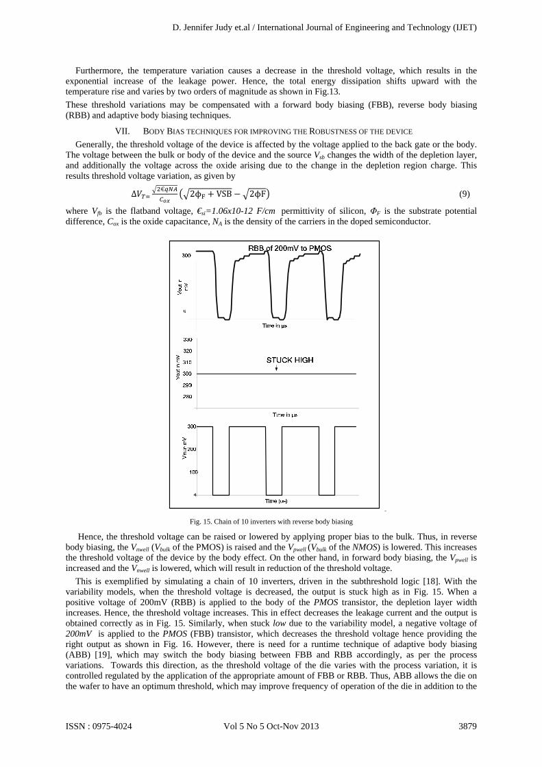
Furthermore, the temperature variation causes a decrease in the threshold voltage, which results in the exponential increase of the leakage power. Hence, the total energy dissipation shifts upward with the temperature rise and varies by two orders of magnitude as shown in Fig.13. These threshold variations may be compensated with a forward body biasing (FBB), reverse body biasing (RBB) and adaptive body biasing techniques.
VII. BODY BIAS TECHNIQUES FOR IMPROVING THE ROBUSTNESS OF THE DEVICE Generally, the threshold voltage of the device is affected by the voltage applied to the back gate or the body.
The voltage between the bulk or body of the device and the source Vsb changes the width of the depletion layer, and additionally the voltage across the oxide arising due to the change in the depletion region charge. This results threshold voltage variation, as given by
∆ € 2 F VSB 2 F (9)
where Vfb is the flatband voltage, €si=1.06x10⁻¹² F/cm permittivity of silicon, ΦF is the substrate potential difference, Cox is the oxide capacitance, NA is the density of the carriers in the doped semiconductor.
Fig. 15. Chain of 10 inverters with reverse body biasing
Hence, the threshold voltage can be raised or lowered by applying proper bias to the bulk. Thus, in reverse body biasing, the Vnwell (Vbulk of the PMOS) is raised and the Vpwell (Vbulk of the NMOS) is lowered. This increases the threshold voltage of the device by the body effect. On the other hand, in forward body biasing, the Vpwell is increased and the Vnwell is lowered, which will result in reduction of the threshold voltage.
This is exemplified by simulating a chain of 10 inverters, driven in the subthreshold logic [18]. With the variability models, when the threshold voltage is decreased, the output is stuck high as in Fig. 15. When a positive voltage of 200mV (RBB) is applied to the body of the PMOS transistor, the depletion layer width increases. Hence, the threshold voltage increases. This in effect decreases the leakage current and the output is obtained correctly as in Fig. 15. Similarly, when stuck low due to the variability model, a negative voltage of 200mV is applied to the PMOS (FBB) transistor, which decreases the threshold voltage hence providing the right output as shown in Fig. 16. However, there is need for a runtime technique of adaptive body biasing (ABB) [19], which may switch the body biasing between FBB and RBB accordingly, as per the process variations. Towards this direction, as the threshold voltage of the die varies with the process variation, it is controlled regulated by the application of the appropriate amount of FBB or RBB. Thus, ABB allows the die on the wafer to have an optimum threshold, which may improve frequency of operation of the die in addition to the
D. Jennifer Judy et.al / International Journal of Engineering and Technology (IJET)
ISSN : 0975-4024 Vol 5 No 5 Oct-Nov 2013 3879

power efficiency consideration. Thus, the combined effect of the parameter variations is compensated by changing the threshold voltage of the device.
Fig. 16. Chain of 10 inverters with forward body biasing
VIII. SIMULATION RESULTS OF THE BENCHMARK CIRCUITS IN THE SUBTHRESHOLD REGION AND THEIR ANALYSIS All the analyses presented so far employ an 8 bit CLA adder as the benchmark circuit. The simulation of 4
bit, 8 bit and 16 bit CLA Adder at supply voltages of value 0.3V and 1.1V in the weak and strong inversion region respectively, operating at a frequency range of 10KHz - 1MHz in the PTM 45nm technology node [20] is depicted in the Fig. 17. and Fig. 18. It precisely exemplifies the logic depth that can be driven by the subthreshold Logic. The power dissipation rises along with increase in the number of bits processed by the adder.
Fig. 17. Power plot of the CLA adders in the strong and weak inversion region
In subthreshold regime, the limiting factor is the delay. Hence, in some ultra low power applications, where the power is of vital importance rather than the delay, the power can be traded off for delay. Recognizing the power-delay product (PDP) as an important factor in the subthreshold operation, Fig. 18 depicts the power-delay product of various adder circuits, operated in strong and weak inversion regions. Further, the simulated results
D. Jennifer Judy et.al / International Journal of Engineering and Technology (IJET)
ISSN : 0975-4024 Vol 5 No 5 Oct-Nov 2013 3880

of the 8 bit CLA adder circuit depicting both the dynamic power and static power dissipation over a wide range of supply voltage from 0.2V to 0.5V at the operating frequency of 10KHz in the 45nm technology node is also presented in the Fig. 19. The static power has been measured with no switching at the input nodes, while the dynamic power for the given range of circuits have been measured with a constant input applied, across all the circuits, for justifiable comparisons.
Fig. 18 Plot of PDP in the strong and weak inversion region
Fig. 19 Simulated Results of the 8 bit CLA adder for both dynamic and static power dissipation over a wide range of supply voltage.
IX. CHANNEL UPSIZING IN THE SUBTHRESHOLD REGIME RESOLVES SUBTHRESHOLD ISSUES: Subthreshold logic faces a number of challenges that needs to be addressed effectively for optimum
performance. Channel upsizing is a reliable solution for improving the following: • Subthreshold Swing • DIBL • Variability • Energy Gain.
D. Jennifer Judy et.al / International Journal of Engineering and Technology (IJET)
ISSN : 0975-4024 Vol 5 No 5 Oct-Nov 2013 3881

Fig. 20. Channel upsizing lowers the Vddopt
Fig. 21 Channel upsizing lowers the Estat and ET
The analyses of the benchmark circuits using 45nm technology node made, at an operating frequency range of 10KHz-100KHz is illustrated in the Fig. 20 and Fig. 21. It depicts the performance improvements realized in the factors mentioned above. Upsizing the channel length from 15nm till 45nm leads to the increase of Leff, since LG ≈Leff. The DIBL coefficient is identified as
with the factor (10)
Eqn. 10 clearly shows the negative exponential dependence of η on Leff. Thus, the channel upsizing mitigates the increase in the DIBL effect created by the scaling. This would lead to a drastic decrease of the leakage current due to the lowering of DIBL effect and the rise in threshold voltage. Besides, the subthreshold leakage current I0 is dramatically lowered as the threshold voltage increases due to the short channel effects by channel upsizing. Thus, this further lowers the optimum supply voltage Vddopt as shown in Fig. 20. It has been illustrated with the simulation results in Fig. 21. The increase of the channel length from 15nm to 45nm results in energy reduction of two orders of magnitude. Thus, the non-minimum channel length is the straight forward circuit level design technique that can be employed to improve the energy efficiency of subthreshold circuits. Finally,
D. Jennifer Judy et.al / International Journal of Engineering and Technology (IJET)
ISSN : 0975-4024 Vol 5 No 5 Oct-Nov 2013 3882

as σVT is proportional to 1/√WLeff, the increase of the channel length may decrease the variability in the threshold voltage due to the process variations and hence balances the robustness of the device.
X. CONCLUSION The subthreshold logic is the most preferable technique in energy constrained systems such as portable or
remote devices where the battery life is the vital control parameter. This paper demonstrated the performance of the circuits in the subthreshold regime. The beneficial and unfavorable effects of subthreshold operation have been delved deeper, with emphasis on ways and means to overcome the limitations of subthreshold operation. The significance of operating the circuits in the minimum energy point at optimum Vdd and optimum VT for improved power efficiency has been highlighted. The trade-off between operating the circuit at minimum energy point and the speed has further been validated, for specific applications involving higher speed of operation at the cost of slightly increased power. The use of the design techniques such as FBB, ABB and ABRM for addressing the nature of increased sensitivity of the device, for process variations while operating in the weak inversion region has been discussed. As a future endeavor, it is plausible to investigate nascent technologies like DG-MOSFETs, and Finfets in the subthreshold regime.
REFERENCES [1] A.Wang, B. Calhoun, and A. Chandrakasan, Sub-Threshold Design for Ultra Low-Power Systems. New York: Springer, 2006. [2] H. Soeleman and K. Roy, “Ultra-low power digital subthreshold logic circuits,” in Proc. IEEE /ACM Int. Symp. Low-Power
Electron. Des., 1999, pp. 94–96. [3] H. Soeleman, K. Roy, and B. C. Paul, “Robust subthreshold logic for ultra-low power operation,” IEEE Trans. Very Large Scale
Integr.(VLSI) Syst., vol. 9, no. 1, pp. 90–99, Jan. 2001. [4] D. Bol, R. Ambroise, D. Flandre, and J.-D. Legat, “Interests and limitations of technology scaling for subthreshold logic,” IEEE Trans.
Very Large Scale Integr. (VLSI) Syst., vol. 17, No. 10, pp. 1508–1519, Oct.2009. [5] B. C. Paul, A. Raychowdhury, and K. Roy, “Device optimization for digital subthreshold logic operation,” IEEE Trans. Electron
Devices,vol. 52, no. 2, pp. 237–247, Feb. 2005. [6] Massimo Alioto, “Ultra-Low Power VLSI Circuit Design Demystified and Explained: A Tutorial,” IEEE Trans. on Circuits and
System—I: Regular Papers, vol.59, no. 1, pp.3-29,Jan 2012. [7] D. Bol, R. Ambroise, D. Flandre, and J.-D. Legat, “Impact of technology scaling on digital subthreshold circuits,” in Proc. IEEE
Annu. Comput. Soc. Int. Conf. VLSI, 2008, pp. 179–184. [8] S. Hanson, M. Seok, D. Sylvester, and D. Blaauw, “Nanometer device scaling in subthreshold logic and SRAM,” IEEE Trans.
Electron Devices, vol. 55, no. 1, pp. 175–185, Jan. 2008. [9] B. H. Calhoun, A. Wang, and A. P. Chandrakasan, “Modeling and sizing for minimum energy operation in subthreshold circuits,”
IEEE J. Solid-State Circuits, vol. 40, no. 9, pp. 1778–1786, Sep. 2005. [10] D. Bol, D. Kamel, D. Flandre and J.-D. Legat, “Nanometer MOSFET effects on the minimum-energy point of 45nm subthreshold
logic”, in Proc. ACM/IEEE Int. Symp. Low-Power Electron. Des, 6 p, 2009. [11] J. Rabaey, M. Pedram, and P. Landman, Low Power Design Methodologies, Boston: Kluwer Academic Publishers, 1995. [12] A. P. Chandrakasan and R.W. Brodersen, “Minimizing power consumption in digital CMOS circuits,” Proc. IEEE, vol. 83,
pp. 498–523, Apr. 1995. [13] B. Zhai et al., “Analysis and mitigation of variability in subthreshold design,” in Proc. ISLPED, Aug. 2005, pp. 20–25. [14] A. Raychowdhury, B. C. Paul, and K. Roy, “Computing with subthreshold leakage: Device/circuit/architecture co-design for ULP
subthreshold operation,” IEEE Trans. Very Large Scale Integr. (VLSI) Syst., vol. 13, no. 11, pp. 1213–1224, Nov. 2005. [15] E. Vittoz, “Weak inversion for ultimate low-power logic,” in Low-Power Electronics Design, C. Piguet, Ed. Boca Raton, FL: CRC,
2005. [16] M. Alioto, G. Palumbo, and M. Pennisi, “Understanding the effect of process variations on the delay of static and domino logic,” IEEE
Trans. Very Large Scale Integr. (VLSI) Syst., vol. 18, no. 5, pp. 697–710, May 2010. [17] S. Hanson, B. Zhai, M. Seok, B. Cline, K. Zhou, M. Singhal, M. Minuth, J. Olson, L. Nazhandali, T. Austin, D. Sylvester and D.
Blaauw, “Exploring variability and performance in a sub-200-mV processor,” IEEE J. Solid-State Circuits, vol. 43, no. 4, Apr. 2008. [18] J. Tschanz, J. Kao, and S. Narendra, “Adaptive body bias for reducing impacts of die-to-die and within-die parameter variations on
microprocessor frequency and leakage,” IEEE Journal of Solid-State Circuits, vol. 37, no. 11, pp. 1396–1402, 2002. [19] G. Ono and M. Miyazaki, “Threshold-voltage balance for minimum supply operation [LV CMOS chips],” IEEE Journal of Solid-State
Circuits, vol. 38, 2003. [20] http://ptm.asu.edu BPTM MOSFET Models.
BIOGRAPHIES
D.Jennifer Judy received B.E degree in Electronics and communication from Periyar University in 1999 and M.tech from Dr.MGR University in 2011. She is pursuing her Ph.D in VIT University, Chennai from 2011.
Dr. V.S.Kanchana Bhaaskaran obtained her under graduation degree from Institution of Engineers (India), received her M.S. degree in Systems and Information from Birla Institute of Technology and Sciences, Pilani and PhD degree in the field of Low Power Design of VLSI Circuits from VIT University. She is a Fellow of the Institution of Engineers (India) and a Fellow of the Institution of Electronics and Telecommunication Engineers and Member of IEEE and IET. She has 35 years of industry, research and teaching experience through serving the Department of Employment and Training, Government of Tamil Nadu, Indian Institute of Technology Madras, Salem Cooperative Sugar Mills’ Polytechnic College, SSN College of Engineering and currently she serves as the Professor and Dean of the School of Electronics Engineering of VIT University, Chennai Campus, Chennai, Tamil Nadu, India.
D. Jennifer Judy et.al / International Journal of Engineering and Technology (IJET)
ISSN : 0975-4024 Vol 5 No 5 Oct-Nov 2013 3883