revised electronic supplementary information - the … · · 2009-12-15the same sio2/si...
TRANSCRIPT

Supplementary material (ESI) for Journal of Materials Chemistry This journal is © The Royal Society of Chemistry 2009
Electronic Supplementary Information (ESI †)
All-Organic Coaxial Nanocables with Interfacial Charge-Transfer Layers: Electrical Conductivity and Light-Emitting-Transistor Behavior Jong H. Kima, Akira Watanabeb, Jong Won Chunga, Yunoh Junga, Byeong-Kwan Ana, Hirokazu Tada*b, and Soo Young Park*a Experimental section
MATERIALS
Regioregular P3HT (Mw= 87,000) was purchased from Aldrich Company and used as
received. CN-TFMBE was synthesized by the Suzuki coupling reaction and the Knoevenagel
reaction, following previously published procedures,5 and was then purified by vacuum
sublimation.
Coaxial nanocables were prepared by dissolving binary mixtures of CN-TFMBE and P3HT
in o-dichlorobenzene with gentle heating. Several samples with different ratios of CN-
TFMBE (i.e., 0, 50, 100, and 200%) with respect to P3HT, keeping the concentration of the
latter as 0.1 wt.% in solution were prepared and investigated. All solutions were coated by the
drop-casting method, evaporated at room temperature, and then annealed on a hot plate at
85°C for one hour.
DEVICE FABRICATION
Bottom-contact devices were prepared to measure the electrical conductivity and the
transistor properties of the coaxial nanocables. Before fabrication, Si/SiO2 substrates were
cleaned by sonication in acetone and isopropyl alcohol. Ultraviolet ozone (UVO) was only
applied to those substrates prepared for measuring the electrical conductivity. The deposition
of two 50 nm-thick gold electrodes onto the clean substrates by thermal evaporation was

Supplementary material (ESI) for Journal of Materials Chemistry This journal is © The Royal Society of Chemistry 2009 carried out in a nitrogen-filled glove box under a vacuum of 3x10⁻⁶ Torr. The deposition rate
was 0.2–0.3 nm/s and the channel length and width between the two electrodes was 50 μm
and 1mm, respectively. After cooling, the active layers of pristine P3HT (0.1 wt.%) and the
blended solutions (200% CN-TFMBE with respect to P3HT, keeping the concentration of the
latter as 0.1 wt.% in solution) were drop-cast. After evaporation of the solvent, the samples
were annealed on a heating plate at 85°C for one hour in a nitrogen-filled glove box to
remove any effects due to solvent residues. All the coaxial nanocables with different blending
ratios between P3HT and CN-TFMBE showed enhanced electrical characteristics with
different degrees depending on the uniformity of the coaxial structures.
Interdigital heteroelectrodes for evaluating the light-emitting transistors were fabricated on
the same SiO2/Si substrates using photolithography and lift-off processes. Firstly, Au (30
nm)/Cr (10 nm) source electrodes were formed on the SiO2 layer. Guiding lines for the
succeeding processes were also formed on the substrates. A photomask was then placed at the
exact position referring to the guiding lines to prepare the Al drain electrodes (30 nm). The
channel length (L) and width (W) of the electrodes were 5 µm and 38 mm, respectively. After
fabricating the heteroelectrodes, the same cleaning and device-preparation methods as those
described above were applied.
ELECTRICAL MEASUREMENTS
The current–voltage characteristics for investigating the electrical conductivities and
transistor properties were measured using Keithley 2400 and Keithley 6517 equipments
connected to a probe station. In the case of the light-emitting-transistor measurements, the
electrical characteristics were measured using Keithley 6487 and Keithley 487 instruments.
The light intensity was detected with a Si photodiode placed just above the device, through a
glass window of the vacuum chamber (at a vacuum of 5x10⁻⁶ Torr at room temperature).

Supplementary material (ESI) for Journal of Materials Chemistry This journal is © The Royal Society of Chemistry 2009 Magnifying the sample under the optical microscope which is attached to the probe-station,
we were able to cut the individual coaxial nanocable using the sharp tip of the probe. I-V
measurements were repeated after disconnecting the individual nanocables. Before
proceeding to the next cutting or I-V measurement, we have thoroughly cleaned the tip using
solvent (acetone) to remove any residuals attached to the tip.
S1
We observed morphology change during coaxial nanocable formation. After drop casting of
blended solution onto the substrate, we measured optical microscopy images with time. CN-
TFMBE nanowires are slowly formed and floating on the solution due to its high self-
assembling power in 30 minutes after drop casting. Then nanowires go down to the bottom of
substrate, P3HT covers them with solvent evaporation and coaxial nanocables are fabricated
as shown in Fig S1.
Fig. S1. Schematic diagram (a) and optical microscopy images (b) explaining a process of coaxial nanocable growth.
Supplementary material (ESI) for Journal of Materials Chemistry This journal is © The Royal Society of Chemistry 2009
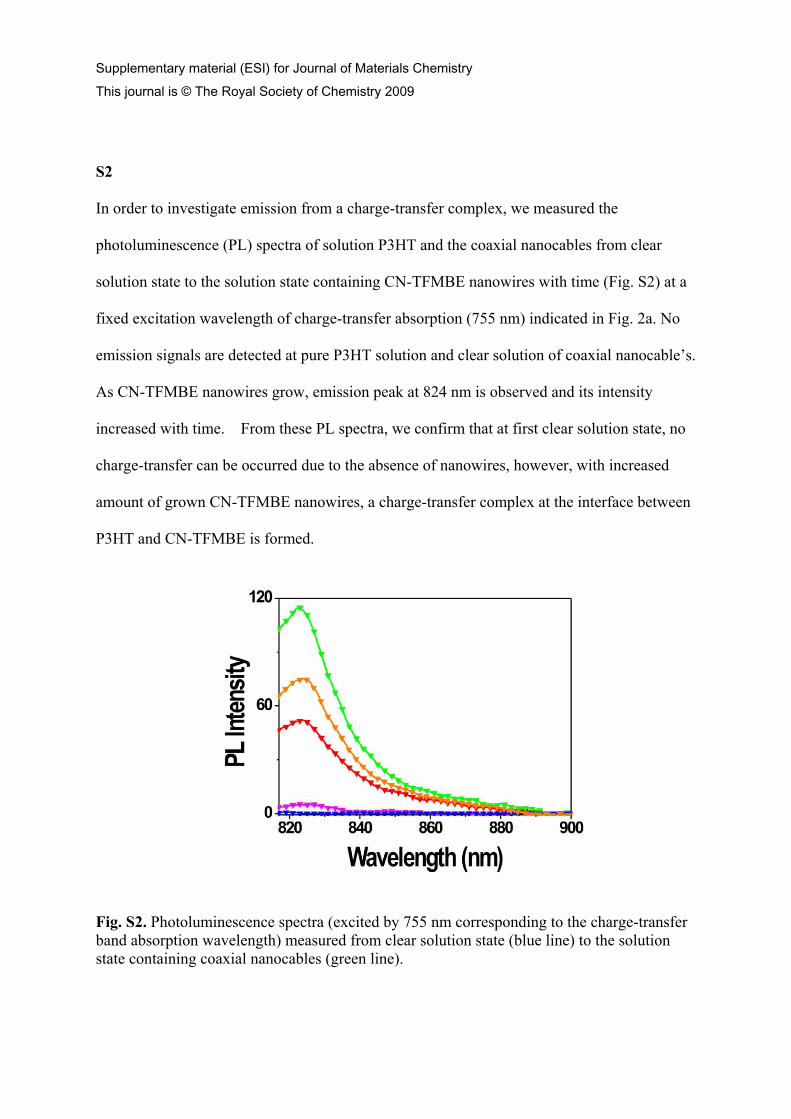
S2
In order to investigate emission from a charge-transfer complex, we measured the
photoluminescence (PL) spectra of solution P3HT and the coaxial nanocables from clear
solution state to the solution state containing CN-TFMBE nanowires with time (Fig. S2) at a
fixed excitation wavelength of charge-transfer absorption (755 nm) indicated in Fig. 2a. No
emission signals are detected at pure P3HT solution and clear solution of coaxial nanocable’s.
As CN-TFMBE nanowires grow, emission peak at 824 nm is observed and its intensity
increased with time. From these PL spectra, we confirm that at first clear solution state, no
charge-transfer can be occurred due to the absence of nanowires, however, with increased
amount of grown CN-TFMBE nanowires, a charge-transfer complex at the interface between
P3HT and CN-TFMBE is formed.
Fig. S2. Photoluminescence spectra (excited by 755 nm corresponding to the charge-transfer band absorption wavelength) measured from clear solution state (blue line) to the solution state containing coaxial nanocables (green line).

Supplementary material (ESI) for Journal of Materials Chemistry This journal is © The Royal Society of Chemistry 2009
S3
Fig. S3. Scanning electron microscopy (a) and optical microscopy (b) images of fabricated devices based on coaxial nanocables.
S4
Fig. S4. Electroluminescence (EL) spectrum (a) and output curve (b) of light emitting organic transistors based on coaxial nanocables during operation.