rf engineering basic concepts: the smith chart · rf engineering basic concepts: the smith chart f....
TRANSCRIPT

arX
iv:1
201.
4068
v1 [
phys
ics.
acc-
ph]
19 J
an 2
012
RF engineering basic concepts: the Smith chart
F. CaspersCERN, Geneva, Switzerland
AbstractThe Smith chart is a very valuable and important tool that facilitates interpre-tation of S-parameter measurements. This paper will give a brief overviewon why and more importantly on how to use the chart. Its definition as wellas an introduction on how to navigate inside the chart are illustrated. Use-ful examples show the broad possibilities for use of the chart in a variety ofapplications.
1 Motivation
With the equipment at hand today, it has become rather easy tomeasure the reflection factorΓ evenfor complicated networks. In the “good old days” though, this was done measuring the electric fieldstrength1 at a coaxial measurement line with a slit at different positions in the axial direction (Fig. 1). A
DUT
from
generator
movable electric field probe
Umin
Umax
Fig. 1: Schematic view of a measurement set–up used to determine thereflection coefficient as well as the voltagestanding wave ratio of a device under test (DUT) [1]
small electric field probe, protruding into the field region of the coaxial line near the outer conductor,was moved along the line. Its signal was picked up and displayed on a microvoltmeter after rectificationvia a microwave diode. While moving the probe, field maxima and minima as well as their position andspacing could be found. From this the reflection factorΓ and theVoltageStandingWaveRatio (VSWRor SWR) could be determined using the following definitions:
– Γ is defined as the ratio of the electrical field strengthE of the reflected wave over the forwardtravelling wave:
Γ =E of reflected wave
E of forward traveling wave. (1)
1The electrical field strength was used since it can be measured considerably more easily than the magnetic field strength.

– The VSWR is defined as the ratio of maximum to minimum measured voltage:
VSWR=Umax
Umin=
1 + |Γ|1− |Γ| . (2)
Although today these measurements are far easier to conduct, the definitions of the aforementionedquantities are still valid. Also their importance has not diminished in the field of microwave engineeringand so the reflection coefficient as well as the VSWR are still avital part of the everyday life of amicrowave engineer be it for simulations or measurements.
A special diagram is widely used to visualize and to facilitate the determination of these quantities.Since it was invented in 1939 by the engineer Phillip Smith, it is simply known as the Smith chart [2].
2 Definition of the Smith chart
The Smith chart provides a graphical representation ofΓ that permits the determination of quantitiessuch as the VSWR or the terminating impedance of a device under test (DUT). It uses a bilinear Moebiustransformation, projecting the complex impedance plane onto the complexΓ plane:
Γ =Z − Z0
Z + Z0with Z = R+ j X . (3)
As can be seen in Fig. 2 the half-plane with positive real partof impedanceZ is mapped onto the interiorof the unit circle of theΓ plane. For a detailed calculation see Appendix A.
Im (Γ)
Re (Γ)
X = Im (Z)
R = Re (Z)
Fig. 2: Illustration of the Moebius transform from the complex impedance plane to theΓ plane commonly knownas Smith chart
2.1 Properties of the transformation
In general, this transformation has two main properties:
– generalized circles are transformed into generalized circles (note that a straight line is nothing elsethan a circle with infinite radius and is therefore mapped as acircle in the Smith chart);
– angles are preserved locally.
Figure 3 illustrates how certain basic shapes transform from the impedance to theΓ plane.
2

Im (Γ)
Re (Γ)
X = Im (Z)
R = Re (Z)
Fig. 3: Illustration of the transformation of basic shapes from theZ to theΓ plane
2.2 Normalization
The Smith chart is usually normalized to a terminating impedanceZ0 (= real):
z =Z
Z0. (4)
This leads to a simplification of the transform:
Γ =z − 1
z + 1⇔ z =
1 + Γ
1− Γ. (5)
AlthoughZ = 50Ω is the most common reference impedance (characteristic impedance of coaxial ca-bles) and many applications use this normalization, any other real and positive value is possible.There-fore it is crucial to check the normalization before using any chart.
Commonly used charts that map the impedance plane onto theΓ plane always look confusing atfirst, as many circles are depicted (Fig. 4). Keep in mind thatall of them can be calculated as shown inAppendix A and that this representation is the same as shown in all previous figures — it just containsmore circles.
2.3 Admittance plane
The Moebius transform that generates the Smith chart provides also a mapping of the complex admittanceplane (Y = 1
Zor normalizedy = 1
z) into the same chart:
Γ = −y − 1y + 1
= −Y − Y0
Y + Y0= −1/Z − 1/Z0
1/Z + 1/Z0=
Z − Z0
Z + Z0=
z − 1z + 1
. (6)
Using this transformation, the result is the same chart, butmirrored at the centre of the Smith chart(Fig. 5). Often both mappings, the admittance and the impedance plane, are combined into one chart,which looks even more confusing (see last page). For reasonsof simplicity all illustrations in this paperwill use only the mapping from the impedance to theΓ plane.
3

0.00
0.01
0.02
0.03
0.04
0.05
0.06
0.07
0.08
0.09
0.10
0.110.12 0.13
0.14
0.15
0.16
0.17
0.18
0.19
0.20
0.21
0.22
0.23
0.24
0.25
0.26
0.27
0.28
0.29
0.30
0.31
0.32
0.33
0.34
0.35
0.360.370.38
0.39
0.40
0.41
0.42
0.43
0.44
0.45
0.46
0.47
0.48
0.49
0.00
0.01
0.02
0.03
0.04
0.05
0.06
0.07
0.08
0.09
0.10
0.110.12 0.13 0.14
0.15
0.16
0.17
0.18
0.19
0.20
0.21
0.22
0.23
0.24
0.25
0.26
0.27
0.28
0.29
0.30
0.31
0.32
0.33
0.34
0.350.36
0.370.380.39
0.40
0.41
0.42
0.43
0.44
0.45
0.46
0.47
0.48
0.49
010
20
30
40
50
60
70
8090
100
110
120
130
140
150
160
170
180
-170
-160
-150
-140
-130
-120
-110
-100 -90-80
-70
-60
-50
-40
-30
-20
-10
0.1
0.2
0.3
0.4
0.5
0.6
0.7
0.8
0.9
1.0
1.2
1.4
1.6
1.8
2.0
3.0
4.0
5.0
10
20
50
0.2
0.2
0.4
0.4
0.6
0.6
0.8
0.8
1
1
10.90.8
0.7
0.6
0.5
0.4
0.3
0.2
0.1
0
2
3
4
5
10
20
50
1.21.4
1.6
1.8
0.05
0.15
-1-0.9-0.
8-0
.7
-0.6
-0.5
-0.4
-0.3
-0.2
-0.1
-2
-3
-4
-5
-10
-20
-50
-1.2
-1.4
-1.6
-1.8
-0.05
-0.15
Fig. 4: Example of a commonly used Smith chart
3 Navigation in the Smith chart
The representation of circuit elements in the Smith chart isdiscussed in this section starting with theimportant points inside the chart. Then several examples ofcircuit elements will be given and theirrepresentation in the chart will be illustrated.
3.1 Important points
There are three important points in the chart:
1. Open circuit withΓ = 1, z → ∞2. Short circuit withΓ = −1, z = 0
3. Matched load withΓ = 0, z = 1
They all are located on the real axis at the beginning, the end, and the centre of the circle (Fig. 6). Theupper half of the chart is inductive, since it corresponds tothe positive imaginary part of the impedance.The lower half is capacitive as it is corresponding to the negative imaginary part of the impedance.
4

Im (Γ)
Re (Γ)
B = Im (Y )
G = Re (Y )
Γ = −Y−Y0Y+Y0
with Y = G+ j B
Fig. 5: Mapping of the admittance plane into theΓ plane
Im (Γ)
Re (Γ)
matched load
short circuit open circuit
Fig. 6: Important points in the Smith chart
Concentric circles around the diagram centre represent constant reflection factors (Fig. 7). Theirradius is directly proportional to the magnitude ofΓ, therefore a radius of 0.5 corresponds to reflection of3 dB (half of the signal is reflected) whereas the outermost circle (radius = 1) represents full reflection.Therefore matching problems are easily visualized in the Smith chart since a mismatch will lead to areflection coefficient larger than 0 (Eq. (7)).
Power into the load = forward power - reflected power:P =1
2
(
|a|2 − |b|2)
=|a|22
(
1− |Γ|2)
. (7)
5

0.00
0.01
0.02
0.03
0.04
0.05
0.06
0.07
0.08
0.09
0.10
0.110.12 0.13
0.14
0.15
0.16
0.17
0.18
0.19
0.20
0.21
0.22
0.23
0.24
0.25
0.26
0.27
0.28
0.29
0.30
0.31
0.32
0.33
0.34
0.35
0.360.370.38
0.39
0.40
0.41
0.42
0.43
0.44
0.45
0.46
0.47
0.48
0.49
0.00
0.01
0.02
0.03
0.04
0.05
0.06
0.07
0.08
0.09
0.10
0.110.12 0.13 0.14
0.15
0.16
0.17
0.18
0.19
0.20
0.21
0.22
0.23
0.24
0.25
0.26
0.27
0.28
0.29
0.30
0.31
0.32
0.33
0.34
0.350.36
0.370.380.39
0.40
0.41
0.42
0.43
0.44
0.45
0.46
0.47
0.48
0.49
010
20
30
40
50
60
70
8090
100
110
120
130
140
150
160
170
180
-170
-160
-150
-140
-130
-120
-110
-100 -90-80
-70
-60
-50
-40
-30
-20
-10
0.1
0.2
0.3
0.4
0.5
0.6
0.7
0.8
0.9
1.0
1.2
1.4
1.6
1.8
2.0
3.0
4.0
5.0
10
20
50
0.2
0.2
0.4
0.4
0.6
0.6
0.8
0.8
1
1
10.90.8
0.7
0.6
0.5
0.4
0.3
0.2
0.1
0
2
3
4
5
10
20
50
1.21.4
1.6
1.8
0.05
0.15
-1-0.9-0.
8-0
.7
-0.6
-0.5
-0.4
-0.3
-0.2
-0.1
-2
-3
-4
-5
-10
-20
-50
-1.2
-1.4
-1.6
-1.8
-0.05
-0.15
|Γ| = 1|Γ| = 0.75|Γ| = 0.5|Γ| = 0.25|Γ| = 0
Fig. 7: Illustration of circles representing a constant reflectionfactor
In Eq. (7) the European notation2 is used, where power =|a|2
2 . Furthermore(1−|Γ|2) corresponds to themismatch loss.
Although only the mapping of the impedance plane to theΓ plane is used, one can easily use it todetermine the admittance since
Γ(1
z) =
1z− 1
1z+ 1
=1− z
1 + z=
(
z − 1
z + 1
)
or Γ(1
z) = −Γ(z) . (8)
In the chart this can be visualized by rotating the vector of acertain impedance by 180 (Fig. 8).
0.00
0.01
0.02
0.03
0.04
0.05
0.06
0.07
0.08
0.09
0.10
0.110.12 0.13
0.14
0.15
0.16
0.17
0.18
0.19
0.20
0.21
0.22
0.23
0.24
0.25
0.26
0.27
0.28
0.29
0.30
0.31
0.32
0.33
0.34
0.35
0.360.370.38
0.39
0.40
0.41
0.42
0.43
0.44
0.45
0.46
0.47
0.48
0.49
0.00
0.01
0.02
0.03
0.04
0.05
0.06
0.07
0.08
0.09
0.10
0.110.12 0.13 0.14
0.15
0.16
0.17
0.18
0.19
0.20
0.21
0.22
0.23
0.24
0.25
0.26
0.27
0.28
0.29
0.30
0.31
0.32
0.33
0.34
0.350.36
0.370.380.39
0.40
0.41
0.42
0.43
0.44
0.45
0.46
0.47
0.48
0.49
010
20
30
40
50
60
70
8090
100
110
120
130
140
150
160
170
180
-170
-160
-150
-140
-130
-120
-110
-100 -90-80
-70
-60
-50
-40
-30
-20
-10
0.1
0.2
0.3
0.4
0.5
0.6
0.7
0.8
0.9
1.0
1.2
1.4
1.6
1.8
2.0
3.0
4.0
5.0
10
20
50
0.2
0.2
0.4
0.4
0.6
0.6
0.8
0.8
1
1
10.90.8
0.7
0.6
0.5
0.4
0.3
0.2
0.1
0
2
3
4
5
10
20
50
1.21.4
1.6
1.8
0.05
0.15
-1-0.9-0.
8-0
.7
-0.6
-0.5
-0.4
-0.3
-0.2
-0.1
-2
-3
-4
-5
-10
-20
-50
-1.2
-1.4
-1.6
-1.8
-0.05
-0.15
ImpedancezReflectionΓ
Admittancey =1z
Reflection -Γ
Fig. 8: Conversion of an impedance to the corresponding emittance in the Smith chart
2The commonly used notation in the US is power =|a|2. These conventions have no impact on S parameters but they arerelevant for absolute power calculation. Since this is rarely used in the Smith chart, the definition used is not criticalfor thispaper.
6

3.2 Adding impedances in series and parallel (shunt)
A lumped element with variable impedance connected in series is an example of a simple circuit. Thecorresponding signature of such a circuit for a variable inductance and a variable capacitor is a circle. De-pending on the type of impedance, this circle is passed through clockwise (inductance) or anticlockwise(Fig. 9). If a lumped element is added in parallel, the situation is the same as for an element connected in
0.00
0.01
0.02
0.03
0.04
0.05
0.06
0.07
0.08
0.09
0.10
0.110.12 0.13
0.14
0.15
0.16
0.17
0.18
0.19
0.20
0.21
0.22
0.23
0.24
0.25
0.26
0.27
0.28
0.29
0.30
0.31
0.32
0.33
0.34
0.35
0.360.370.38
0.39
0.40
0.41
0.42
0.43
0.44
0.45
0.46
0.47
0.48
0.49
0.00
0.01
0.02
0.03
0.04
0.05
0.06
0.07
0.08
0.09
0.10
0.110.12 0.13 0.14
0.15
0.16
0.17
0.18
0.19
0.20
0.21
0.22
0.23
0.24
0.25
0.26
0.27
0.28
0.29
0.30
0.31
0.32
0.33
0.34
0.350.36
0.370.380.39
0.40
0.41
0.42
0.43
0.44
0.45
0.46
0.47
0.48
0.49
010
20
30
40
50
60
70
8090
100
110
120
130
140
150
160
170
180
-170
-160
-150
-140
-130
-120
-110
-100 -90-80
-70
-60
-50
-40
-30
-20
-10
0.1
0.2
0.3
0.4
0.5
0.6
0.7
0.8
0.9
1.0
1.2
1.4
1.6
1.8
2.0
3.0
4.0
5.0
10
20
50
0.2
0.2
0.4
0.4
0.6
0.6
0.8
0.8
1
1
10.90.8
0.7
0.6
0.5
0.4
0.3
0.2
0.1
0
2
3
4
5
10
20
50
1.21.4
1.6
1.8
0.05
0.15
-1-0.9-0.
8-0
.7
-0.6
-0.5
-0.4
-0.3
-0.2
-0.1
-2
-3
-4
-5
-10
-20
-50
-1.2
-1.4
-1.6
-1.8
-0.05
-0.15
0.00
0.01
0.02
0.03
0.04
0.05
0.06
0.07
0.08
0.09
0.10
0.110.12 0.13
0.14
0.15
0.16
0.17
0.18
0.19
0.20
0.21
0.22
0.23
0.24
0.25
0.26
0.27
0.28
0.29
0.30
0.31
0.32
0.33
0.34
0.35
0.360.370.38
0.39
0.40
0.41
0.42
0.43
0.44
0.45
0.46
0.47
0.48
0.49
0.00
0.01
0.02
0.03
0.04
0.05
0.06
0.07
0.08
0.09
0.10
0.110.12 0.13 0.14
0.15
0.16
0.17
0.18
0.19
0.20
0.21
0.22
0.23
0.24
0.25
0.26
0.27
0.28
0.29
0.30
0.31
0.32
0.33
0.34
0.350.36
0.370.380.39
0.40
0.41
0.42
0.43
0.44
0.45
0.46
0.47
0.48
0.49
010
20
30
40
50
60
70
8090
100
110
120
130
140
150
160
170
180
-170
-160
-150
-140
-130
-120
-110
-100 -90-80
-70
-60
-50
-40
-30
-20
-10
0.1
0.2
0.3
0.4
0.5
0.6
0.7
0.8
0.9
1.0
1.2
1.4
1.6
1.8
2.0
3.0
4.0
5.0
10
20
50
0.2
0.2
0.4
0.4
0.6
0.6
0.8
0.8
1
1
10.90.8
0.7
0.6
0.5
0.4
0.3
0.2
0.1
0
2
3
4
5
10
20
50
1.21.4
1.6
1.8
0.05
0.15
-1-0.9-0.
8-0
.7
-0.6
-0.5
-0.4
-0.3
-0.2
-0.1
-2
-3
-4
-5
-10
-20
-50
-1.2
-1.4
-1.6
-1.8
-0.05
-0.15
SeriesL
Z
SeriesC
Z
Fig. 9: Traces of circuits with variable impedances connected in series
series mirrored by 180 (Fig. 10). This corresponds to taking the same points in the admittance mapping.Summarizing both cases, one ends up with a simple rule for navigation in the Smith chart:
For elements connected in series use the circles in the impedance plane. Go clockwise for an addedinductance and anticlockwise for an added capacitor. For elements in parallel use the circles in theadmittance plane. Go clockwise for an added capacitor and anticlockwise for an added inductance.
This rule can be illustrated as shown in Fig. 11
3.3 Impedance transformation by transmission line
The S matrix of an ideal, lossless transmission line of length l is given by
S =
[
0 e−jβl
e−jβl 0
]
(9)
whereβ = 2πλ
is the propagation coefficient with the wavelengthλ (λ = λ0 for ǫr = 1).
When adding a piece of coaxial line, we turn clockwise on the corresponding circle leading to atransformation of the reflection factorΓload (without line) to the new reflection factorΓin = Γloade−j2βl.Graphically speaking, this means that the vector corresponding toΓin is rotated clockwise by an angle of2βl (Fig. 12).
7

0.000.01
0.02
0.03
0.04
0.05
0.06
0.07
0.08
0.09
0.10
0.11
0.12
0.13
0.14
0.15
0.16
0.17
0.18
0.19
0.20
0.21
0.22
0.23
0.24 0.250.26
0.27
0.28
0.29
0.30
0.31
0.32
0.33
0.34
0.35
0.36
0.37
0.38
0.39
0.40
0.41
0.42
0.43
0.44
0.45
0.46
0.47
0.48
0.49
0.00 0.010.02
0.03
0.04
0.05
0.06
0.07
0.08
0.09
0.10
0.11
0.12
0.13
0.14
0.15
0.16
0.17
0.18
0.19
0.20
0.21
0.220.23
0.240.250.260.2
70.
28
0.29
0.30
0.31
0.32
0.33
0.34
0.35
0.36
0.37
0.38
0.39
0.40
0.41
0.42
0.43
0.44
0.45
0.46
0.47
0.48
0.49
010
20
30
40
50
60
70
80
90
100
110
120
130
140
150
160
170180
-170
-160
-150
-140
-130
-120
-110
-100
-90
-80
-70
-60
-50
-40
-30
-20
-10
0.1
0.2
0.3
0.4
0.5
0.6
0.7
0.8
0.9
1.0
1.2
1.4
1.6
1.8
2.0
3.0
4.0
5.0
10
20
50
0.2
0.2
0.4
0.4
0.6
0.6
0.8
0.8
1
1
10.9
0.8
0.7
0.6
0.5
0.4
0.3
0.2
0.10
2
3
4
5
102050
1.2
1.4
1.6
1.8
0.050.15
-1
-0.9
-0.8
-0.7
-0.6
-0.5
-0.4
-0.3
-0.2
-0.1
-2
-3
-4
-5
-10 -20 -50
-1.2
-1.4
-1.6
-1.8
-0.05
-0.15
ShuntL
ZS
huntCZ
Fig.10:T
raceso
fcircuits
with
variable
imp
edan
cesco
nn
ectedin
pa
rallel
0.000.01
0.02
0.03
0.04
0.05
0.06
0.07
0.08
0.09
0.10
0.11
0.12
0.13
0.14
0.15
0.16
0.17
0.18
0.19
0.20
0.21
0.22
0.23
0.24 0.250.26
0.27
0.28
0.29
0.30
0.31
0.32
0.33
0.34
0.35
0.36
0.37
0.38
0.39
0.40
0.41
0.42
0.43
0.44
0.45
0.46
0.47
0.48
0.49
0.00 0.010.02
0.03
0.04
0.05
0.06
0.07
0.08
0.09
0.10
0.11
0.12
0.13
0.14
0.15
0.16
0.17
0.18
0.19
0.20
0.21
0.220.23
0.240.250.260.2
70.
28
0.29
0.30
0.31
0.32
0.33
0.34
0.35
0.36
0.37
0.38
0.39
0.40
0.41
0.42
0.43
0.44
0.45
0.46
0.47
0.48
0.49
010
20
30
40
50
60
70
80
90
100
110
120
130
140
150
160
170180
-170
-160
-150
-140
-130
-120
-110
-100
-90
-80
-70
-60
-50
-40
-30
-20
-10
0.1
0.2
0.3
0.4
0.5
0.6
0.7
0.8
0.9
1.0
1.2
1.4
1.6
1.8
2.0
3.0
4.0
5.0
10
20
50
0.2
0.2
0.4
0.4
0.6
0.6
0.8
0.8
1
1
10.9
0.8
0.7
0.6
0.5
0.4
0.3
0.2
0.10
2
3
4
5
102050
1.2
1.4
1.6
1.8
0.050.15
-1
-0.9
-0.8
-0.7
-0.6
-0.5
-0.4
-0.3
-0.2
-0.1
-2
-3
-4
-5
-10 -20 -50
-1.2
-1.4
-1.6
-1.8
-0.05
-0.15
SeriesL
SeriesC
ShuntC
ShuntL
Fig.11:Illu
stration
ofn
avigatio
nin
the
Sm
ithch
artwh
enad
din
glu
mp
edelem
ents
8

0.00
0.01
0.02
0.03
0.04
0.05
0.06
0.07
0.08
0.09
0.10
0.110.12 0.13
0.14
0.15
0.16
0.17
0.18
0.19
0.20
0.21
0.22
0.23
0.24
0.25
0.26
0.27
0.28
0.29
0.30
0.31
0.32
0.33
0.34
0.35
0.360.370.38
0.39
0.40
0.41
0.42
0.43
0.44
0.45
0.46
0.47
0.48
0.49
0.00
0.01
0.02
0.03
0.04
0.05
0.06
0.07
0.08
0.09
0.10
0.110.12 0.13 0.14
0.15
0.16
0.17
0.18
0.19
0.20
0.21
0.22
0.23
0.24
0.25
0.26
0.27
0.28
0.29
0.30
0.31
0.32
0.33
0.34
0.350.36
0.370.380.39
0.40
0.41
0.42
0.43
0.44
0.45
0.46
0.47
0.48
0.49
010
20
30
40
50
60
70
8090
100
110
120
130
140
150
160
170
180
-170
-160
-150
-140
-130
-120
-110
-100 -90-80
-70
-60
-50
-40
-30
-20
-10
0.1
0.2
0.3
0.4
0.5
0.6
0.7
0.8
0.9
1.0
1.2
1.4
1.6
1.8
2.0
3.0
4.0
5.0
10
20
50
0.2
0.2
0.4
0.4
0.6
0.6
0.8
0.8
1
1
10.90.8
0.7
0.6
0.5
0.4
0.3
0.2
0.1
0
2
3
4
5
10
20
50
1.21.4
1.6
1.8
0.05
0.15
-1-0.9-0.
8-0
.7
-0.6
-0.5
-0.4
-0.3
-0.2
-0.1
-2
-3
-4
-5
-10
-20
-50
-1.2
-1.4
-1.6
-1.8
-0.05
-0.15
Γload
2βl
Γin
Fig. 12: Illustration of adding a transmission line of lengthl to an impedance
The peculiarity of a transmission line is that it behaves either as an inductance, a capacitor, or aresistor depending on its length. The impedance of such a line (if lossless!) is given by
Zin = jZ0 tan(βl) . (10)
The function in Eq. (10) has a pole at a transmission line length of λ/4 (Fig. 13). Therefore adding a
Im (Z)
Re (Z)
inductive
capacitive
λ4
λ2
Fig. 13: Impedance of a transmission line as a function of its lengthl
transmission line with this length results in a change ofΓ by a factor−1:
Γin = Γloade−j2βl = Γloade
−j2( 2πλ)l l=λ
4= Γloade−jπ = −Γload . (11)
Again this is equivalent to changing the original impedancez to its admittance1/z or the clockwisemovement of the impedance vector by 180. Especially when starting with a short circuit (at−1 in theSmith chart), adding a transmission line of lengthλ/4 transforms it into an open circuit (at+1 in theSmith chart).
9
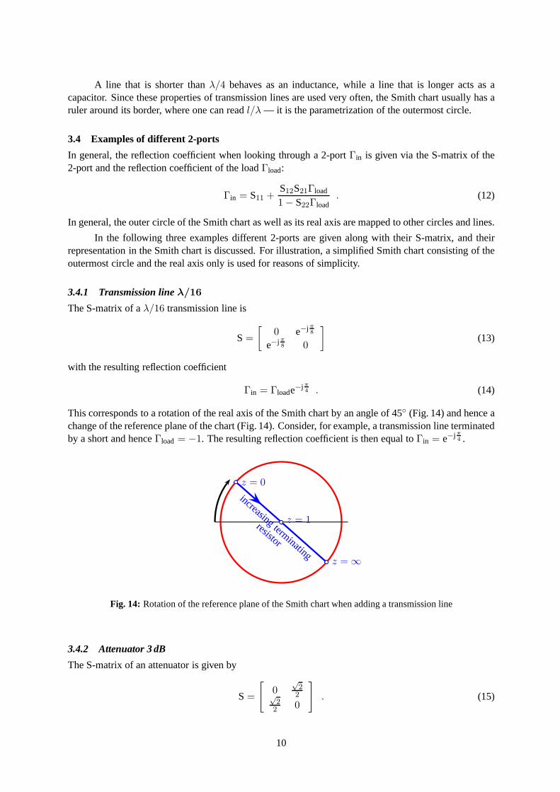
A line that is shorter thanλ/4 behaves as an inductance, while a line that is longer acts as acapacitor. Since these properties of transmission lines are used very often, the Smith chart usually has aruler around its border, where one can readl/λ — it is the parametrization of the outermost circle.
3.4 Examples of different 2-ports
In general, the reflection coefficient when looking through a2-portΓin is given via the S-matrix of the2-port and the reflection coefficient of the loadΓload:
Γin = S11 +S12S21Γload
1− S22Γload. (12)
In general, the outer circle of the Smith chart as well as its real axis are mapped to other circles and lines.
In the following three examples different 2-ports are givenalong with their S-matrix, and theirrepresentation in the Smith chart is discussed. For illustration, a simplified Smith chart consisting of theoutermost circle and the real axis only is used for reasons ofsimplicity.
3.4.1 Transmission line λ/16
The S-matrix of aλ/16 transmission line is
S=
[
0 e−j π8
e−j π8 0
]
(13)
with the resulting reflection coefficient
Γin = Γloade−j π
4 . (14)
This corresponds to a rotation of the real axis of the Smith chart by an angle of 45 (Fig. 14) and hence achange of the reference plane of the chart (Fig. 14). Consider, for example, a transmission line terminatedby a short and henceΓload = −1. The resulting reflection coefficient is then equal toΓin = e−j π
4 .
z = 0
z = 1
z = ∞
increasingterminating
resistor
Fig. 14: Rotation of the reference plane of the Smith chart when adding a transmission line
3.4.2 Attenuator 3 dB
The S-matrix of an attenuator is given by
S=
[
0√22√
22 0
]
. (15)
10
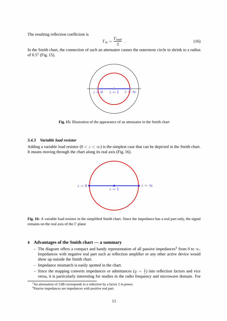
The resulting reflection coefficient is
Γin =Γload
2. (16)
In the Smith chart, the connection of such an attenuator causes the outermost circle to shrink to a radiusof 0.53 (Fig. 15).
z = 0 z = 1 z = ∞
Fig. 15: Illustration of the appearance of an attenuator in the Smithchart
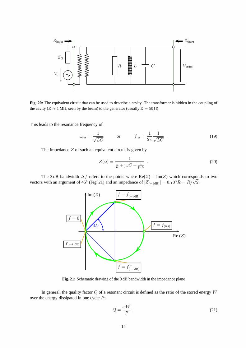
3.4.3 Variable load resistor
Adding a variable load resistor (0< z < ∞) is the simplest case that can be depicted in the Smith chart.It means moving through the chart along its real axis (Fig. 16).
z = 0z = 1
z = ∞
Fig. 16: A variable load resistor in the simplified Smith chart. Sincethe impedance has a real part only, the signalremains on the real axis of theΓ plane
4 Advantages of the Smith chart — a summary– The diagram offers a compact and handy representation of all passive impedances4 from 0 to∞.
Impedances with negative real part such as reflection amplifier or any other active device wouldshow up outside the Smith chart.
– Impedance mismatch is easily spotted in the chart.
– Since the mapping converts impedances or admittances (y = 1z) into reflection factors and vice
versa, it is particularly interesting for studies in the radio frequency and microwave domain. For
3An attenuation of 3 dB corresponds to a reduction by a factor 2in power.4Passive impedances are impedances with positive real part.
11

reasons of convenience, electrical quantities are usuallyexpressed in terms of direct or forwardwaves and reflected or backwards waves in these frequency ranges instead of voltages and currentsused at lower frequencies.
– The transition between impedance and admittance in the chart is particularly easy:Γ(y = 1z) =
−Γ(z).
– Furthermore the reference plane in the Smith chart can be moved very easily by adding a trans-mission line of proper length (Section 3.4.1).
– Many Smith charts have rulers below the complexΓ plane from which a variety of quantities suchas the return loss can be determined. For a more detailed discussion see Appendix B.
5 Examples for applications of the Smith chart
In this section two practical examples of common problems are given, where the use of the Smith chartgreatly facilitates their solution.
5.1 A step in characteristic impedance
Consider a junction between two infinitely short cables, onewith a characteristic impedance of 50Ω andthe other with 75Ω (Fig. 17). The waves running into each port are denoted withai (i = 1, 2) whereas
Junction between a50Ω and a 75Ω cable(infinitely short cables)
a1
b1
a2
b2
Fig. 17: Illustration of the junction between a coaxial cable with 50Ω characteristic impedance and another with75Ω characteristic impedance respectively. Infinitely short cables are assumed – only the junction is considered
the waves coming out of every point are denoted withbi. The reflection coefficient for port 1 is thencalculated as
Γ1 =Z − Z1
Z + Z1=
75− 50
75 + 50= 0.2 . (17)
Thus the voltage of the reflected wave at port 1 is 20% of the incident wave (a2 = a1 · 0.2) and thereflected power at port 1 is 4%5. From conservation of energy, the transmitted power has to be 96% andit follows thatb22 = 0.96.
A peculiarity here is that the transmitted energy ishigher than the energy of the incident wave,sinceEincident = 1,Ereflected= 0.2 and thereforeEtransmitted= Eincident + Ereflected= 1.2. The transmissioncoefficient t is thust = 1 + Γ. Also note that this structure is not symmetric (S11 6= S22), but onlyreciprocal (S21 = S12).
The visualization of this structure in the Smith chart is easy, since all impedances are real and thusall vectors are located on the real axis (Fig. 18).
As stated before, the reflection coefficient is defined with respect to voltages. For currents its signinverts and thus a positive reflection coefficient in terms ofvoltage definition becomes negative whendefined with respect to current.
5Power is proportional toΓ2 and thus 0.22 = 0.04.
12

0.00
0.01
0.02
0.03
0.04
0.05
0.06
0.07
0.08
0.09
0.10
0.110.12 0.13
0.14
0.15
0.16
0.17
0.18
0.19
0.20
0.21
0.22
0.23
0.24
0.25
0.26
0.27
0.28
0.29
0.30
0.31
0.32
0.33
0.34
0.35
0.360.370.38
0.39
0.40
0.41
0.42
0.43
0.44
0.45
0.46
0.47
0.48
0.49
0.00
0.01
0.02
0.03
0.04
0.05
0.06
0.07
0.08
0.09
0.10
0.110.12 0.13 0.14
0.15
0.16
0.17
0.18
0.19
0.20
0.21
0.22
0.23
0.24
0.25
0.26
0.27
0.28
0.29
0.30
0.31
0.32
0.33
0.34
0.350.36
0.370.380.39
0.40
0.41
0.42
0.43
0.44
0.45
0.46
0.47
0.48
0.49
010
20
30
40
50
60
70
8090
100
110
120
130
140
150
160
170
180
-170
-160
-150
-140
-130
-120
-110
-100 -90-80
-70
-60
-50
-40
-30
-20
-10
0.1
0.2
0.3
0.4
0.5
0.6
0.7
0.8
0.9
1.0
1.2
1.4
1.6
1.8
2.0
3.0
4.0
5.0
10
20
50
0.2
0.2
0.4
0.4
0.6
0.6
0.8
0.8
1
1
10.90.8
0.7
0.6
0.5
0.4
0.3
0.2
0.1
0
2
3
4
5
10
20
50
1.21.4
1.6
1.8
0.05
0.15
-1-0.9-0.
8-0
.7
-0.6
-0.5
-0.4
-0.3
-0.2
-0.1
-2
-3
-4
-5
-10
-20
-50
-1.2
-1.4
-1.6
-1.8
-0.05
-0.15
V1 = a+ b = 1.2
b = +0.2I1Z = a− b −b
Incident wavea = 1
Fig. 18: Visualization of the two-port formed by the two cables of different characteristic impedance
For a more general case, e.g.,Z1 = 50Ω andZ2 = 50 + j80Ω, the vectors in the chart are depictedin Fig. 19.
0.00
0.01
0.02
0.03
0.04
0.05
0.06
0.07
0.08
0.09
0.10
0.110.12 0.13
0.14
0.15
0.16
0.17
0.18
0.19
0.20
0.21
0.22
0.23
0.24
0.25
0.26
0.27
0.28
0.29
0.30
0.31
0.32
0.33
0.34
0.35
0.360.370.38
0.39
0.40
0.41
0.42
0.43
0.44
0.45
0.46
0.47
0.48
0.49
0.00
0.01
0.02
0.03
0.04
0.05
0.06
0.07
0.08
0.09
0.10
0.110.12 0.13 0.14
0.15
0.16
0.17
0.18
0.19
0.20
0.21
0.22
0.23
0.24
0.25
0.26
0.27
0.28
0.29
0.30
0.31
0.32
0.33
0.34
0.350.36
0.370.380.39
0.40
0.41
0.42
0.43
0.44
0.45
0.46
0.47
0.48
0.49
010
20
30
40
50
60
70
8090
100
110
120
130
140
150
160
170
180
-170
-160
-150
-140
-130
-120
-110
-100 -90-80
-70
-60
-50
-40
-30
-20
-10
0.1
0.2
0.3
0.4
0.5
0.6
0.7
0.8
0.9
1.0
1.2
1.4
1.6
1.8
2.0
3.0
4.0
5.0
10
20
50
0.2
0.2
0.4
0.4
0.6
0.6
0.8
0.8
1
1
10.90.8
0.7
0.6
0.5
0.4
0.3
0.2
0.1
0
2
3
4
5
10
20
50
1.21.4
1.6
1.8
0.05
0.15
-1-0.9-0.
8-0
.7
-0.6
-0.5
-0.4
-0.3
-0.2
-0.1
-2
-3
-4
-5
-10
-20
-50
-1.2
-1.4
-1.6
-1.8
-0.05
-0.15
a = 1
b
V1 = a+ b
−bI1Z = a− b
I1a
b
V1
ZG = 50Ω
z = 1
Z = 50+j80Ω
(load impedance)
z = 1+j1.6
Fig. 19: Visualization of the two-port depicted on the left in the Smith chart
5.2 Determination of theQ factors of a cavity
One of the most common cases where the Smith chart is used is the determination of the quality factorof a cavity. This section is dedicated to the illustration ofthis task.
A cavity can be described by a parallelRLC circuit (Fig. 20) where the resonance condition isgiven when:
ωL =1
ωC. (18)
13
ZG
R L C Vbeam
V0
Zinput Zshunt
Fig. 20: The equivalent circuit that can be used to describe a cavity.The transformer is hidden in the coupling ofthe cavity (Z ≈ 1MΩ, seen by the beam) to the generator (usuallyZ = 50Ω)
This leads to the resonance frequency of
ωres=1√LC
or fres=1
2π
1√LC
. (19)
The ImpedanceZ of such an equivalent circuit is given by
Z(ω) =1
1R+ jωC + 1
jωL
. (20)
The 3 dB bandwidth∆f refers to the points where Re(Z) = Im(Z) which corresponds to twovectors with an argument of 45 (Fig. 21) and an impedance of|Z(−3dB)| = 0.707R = R/
√2.
Re (Z)
Im (Z)
45
f = f −(−3dB)
f = f(res)
f = f +(−3dB)
f = 0
f → ∞
Fig. 21: Schematic drawing of the 3 dB bandwidth in the impedance plane
In general, the quality factorQ of a resonant circuit is defined as the ratio of the stored energy Wover the energy dissipated in one cycleP :
Q =ωW
P. (21)
14

TheQ factor for a resonance can be calculated via the 3 dB bandwidth and the resonance frequency:
Q =fres
∆f. (22)
For a cavity, three different quality factors are defined:
– Q0 (unloadedQ): Q factor of the unperturbed system, i. e., the stand alone cavity;
– QL (loadedQ): Q factor of the cavity when connected to generator and measurement circuits;
– Qext (externalQ): Q factor that describes the degeneration ofQ0 due to the generator and diag-nostic impedances.
All theseQ factors are connected via a simple relation:
1
QL=
1
Q0+
1
Qext. (23)
The coupling coefficientβ is then defined as
β =Q0
Qext. (24)
This coupling coefficient is not to be confused with the propagation coefficient of transmission lineswhich is also denoted asβ.
In the Smith chart, a resonant circuit shows up as a circle (Fig. 22, circle shown in the detunedshort position). The larger the circle, the stronger the coupling. Three types of coupling are defineddepending on the range ofbeta (= size of the circle, assuming the circle is in the detuned short position):
0.00
0.01
0.02
0.03
0.04
0.05
0.06
0.07
0.08
0.09
0.10
0.110.12 0.13
0.14
0.15
0.16
0.17
0.18
0.19
0.20
0.21
0.22
0.23
0.24
0.25
0.26
0.27
0.28
0.29
0.30
0.31
0.32
0.33
0.34
0.35
0.360.370.38
0.39
0.40
0.41
0.42
0.43
0.44
0.45
0.46
0.47
0.48
0.49
0.00
0.01
0.02
0.03
0.04
0.05
0.06
0.07
0.08
0.09
0.10
0.110.12 0.13 0.14
0.15
0.16
0.17
0.18
0.19
0.20
0.21
0.22
0.23
0.24
0.25
0.26
0.27
0.28
0.29
0.30
0.31
0.32
0.33
0.34
0.350.36
0.370.380.39
0.40
0.41
0.42
0.43
0.44
0.45
0.46
0.47
0.48
0.49
010
20
30
40
50
60
70
8090
100
110
120
130
140
150
160
170
180
-170
-160
-150
-140
-130
-120
-110
-100 -90-80
-70
-60
-50
-40
-30
-20
-10
0.1
0.2
0.3
0.4
0.5
0.6
0.7
0.8
0.9
1.0
1.2
1.4
1.6
1.8
2.0
3.0
4.0
5.0
10
20
50
0.2
0.2
0.4
0.4
0.6
0.6
0.8
0.8
1
1
10.90.8
0.7
0.6
0.5
0.4
0.3
0.2
0.1
0
2
3
4
5
10
20
50
1.21.4
1.6
1.8
0.05
0.15
-1-0.9-0.
8-0
.7
-0.6
-0.5
-0.4
-0.3
-0.2
-0.1
-2-3
-4
-5
-10
-20
-50
-1.2
-1.4
-1.6
-1.8
-0.05
-0.15
Locus of Im (Z) = Re (Z)
f0
f5
f6f4
f3f1
f2
Fig. 22: Illustration of how to determine the differentQ factors of a cavity in the Smith chart
– Undercritical coupling (0 < β < 1): The radius of resonance circle is smaller than 0.25. Hencethe centre of the chart lies outside the circle.
– Critical coupling (β = 1): The radius of the resonance circle is exactly 0.25. Hence the circletouches the centre of the chart.
15
– Overcritical coupling (1 < β < ∞): The radius of the resonance circle is larger than 0.25. Hencethe centre of the chart lies inside the circle.
In practice, the circle may be rotated around the origin due to the transmission lines between the resonantcircuit and the measurement device.
From the different marked frequency points in Fig. 22 the 3 dBbandwidth and thus the qualityfactorsQ0, QL andQext can be determined as follows:
– The unloadedQ can be determined from f5 and f6. The condition to find these points is Re(Z) =Im(Z) with the resonance circle in the detuned short position.
– The loadedQ can be determined from f1 and f2. The condition to find these points is|Im(S11)| →max.
– The externalQ can be calculated from f3 and f4. The condition to determine these points isZ =±j.
To determine the points f1 to f6 with a network analyzer, the following steps are applicable:
– f1 and f2: Set the marker format to Re(S11) + j Im(S11) and determine the two points, whereIm(S11) = max.
– f3 and f4: Set the marker format toZ and find the two points whereZ = ±j.
– f5 and f6: Set the marker format toZ and locate the two points where Re(Z) = Im(Z).
Appendices
A Transformation of lines with constant real or imaginary part from the impedanceplane to theΓ plane
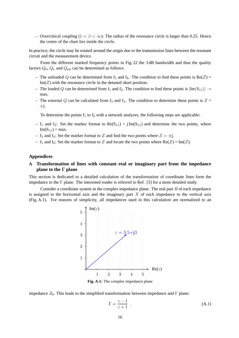
This section is dedicated to a detailed calculation of the transformation of coordinate lines form theimpedance to theΓ plane. The interested reader is referred to Ref. [3] for a more detailed study.
Consider a coordinate system in the complex impedance plane. The real partR of each impedanceis assigned to the horizontal axis and the imaginary partX of each impedance to the vertical axis(Fig. A.1). For reasons of simplicity, all impedances used in this calculation are normalized to an
1
2
3
4
5
1 2 3 4 5Re(z)
Im(z)
z = 3.5+j3
Fig. A.1: The complex impedance plane
impedanceZ0. This leads to the simplified transformation between impedance andΓ plane:
Γ =z − 1
z + 1. (A.1)
16

Γ is a complex number itself:Γ = a+jc. Using this identity and substitutingz = R+ jX in equation(A.1) one obtains
Γ =z − 1
z + 1=
R+ jX − 1
R+ jX + 1= a+ jc . (A.2)
From this the real and the imaginary part ofΓ can be calculated in terms ofa, c, R andX:
Re:a(R + 1)− cX = R− 1; (A.3)
Im: c(R + 1) + aX = X. (A.4)
A.1 Lines with constant real part
To consider lines with constant real part, one can extract anexpression forX from Eq. (A.4):
X = c1 +R
1− a(A.5)
and substitute this into Eq. (A.3):
a2 + c2 − 2aR
1 +R+
R− 1
R+ 1= 0 . (A.6)
Completing the square, one obtains the equation of a circle:
(
a− R
1 +R
)2
+ c2 =1
(1 +R)2. (A.7)
From this equation the following properties can be deduced:
– The centre of each circle lies on the reala axis.
– Since R1+R
≥ 0, the centre of each circle lies on the positive reala axis.
– The radiusρ of each circle follows the equationρ = 1(1+R)2
≤ 1.
– The maximal radius is 1 forR = 0.
A.1.1 Examples
Here the circles for differentR values are calculated and depicted graphically to illustrate the transfor-mation from thez to theΓ plane.
1. R = 0: This leads to the centre coordinates (ca/cc) =(
01+0/0
)
= (0/0), ρ = 11+0 = 1
2. R = 0.5: (ca/cc) =(
0.51+0.5/0
)
= (13/0), ρ = 11+0.5 = 2
3
3. R = 1: (ca/cc) =(
11+1/0
)
= (12/0), ρ = 11+1 = 1
2
4. R = 2: (ca/cc) =(
21+2/0
)
= (23/0), ρ = 11+2 = 1
3
5. R = ∞: (ca/cc) =(
∞1+∞/0
)
= (1/0), ρ = 11+∞ = 0
This leads to the circles depicted in Fig. A.2.
17
R = 0 R = 1
2R = 1 R = 2 R = ∞
Im (Γ)
Re (Γ)
1
−1
1−1
R = 0
R = 1
2
R = 1 R = 21
2
−1
−2
1 2
Im (z)
Re (z)
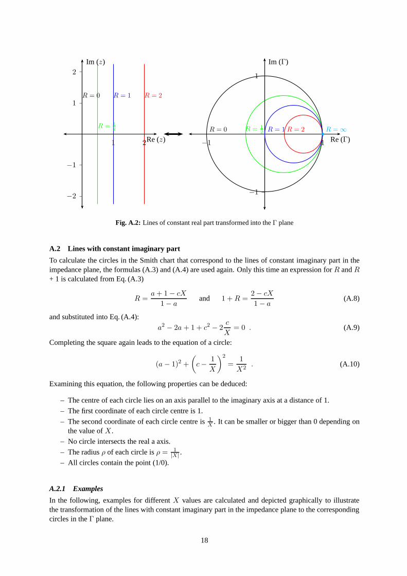
Fig. A.2: Lines of constant real part transformed into theΓ plane
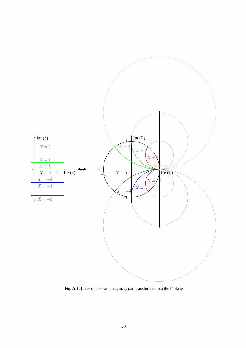
A.2 Lines with constant imaginary part
To calculate the circles in the Smith chart that correspond to the lines of constant imaginary part in theimpedance plane, the formulas (A.3) and (A.4) are used again. Only this time an expression forR andR+ 1 is calculated from Eq. (A.3)
R =a+ 1− cX
1− aand 1 +R =
2− cX
1− a(A.8)
and substituted into Eq. (A.4):
a2 − 2a+ 1 + c2 − 2c
X= 0 . (A.9)
Completing the square again leads to the equation of a circle:
(a− 1)2 +
(
c− 1
X
)2
=1
X2. (A.10)
Examining this equation, the following properties can be deduced:
– The centre of each circle lies on an axis parallel to the imaginary axis at a distance of 1.
– The first coordinate of each circle centre is 1.
– The second coordinate of each circle centre is1X
. It can be smaller or bigger than 0 depending onthe value ofX.
– No circle intersects the real a axis.
– The radiusρ of each circle isρ = 1|X| .
– All circles contain the point (1/0).
A.2.1 Examples
In the following, examples for differentX values are calculated and depicted graphically to illustratethe transformation of the lines with constant imaginary part in the impedance plane to the correspondingcircles in theΓ plane.
18

1. X = -2: (ca/cc) =(
1/ 1−2
)
= (1/ − 0.5), ρ = 1|−2| = 0.5
2. X = -1: (ca/cc) =(
1/ 1−1
)
= (1/ − 1), ρ = 1|−1| = 1
3. X = -0.5: (ca/cc) =(
1/ 1−0.5
)
= (1/ − 2), ρ = 1|−2| = 2
4. X = 0: (ca/cc) =(
1/10
)
= (1/∞), ρ = 1|0| = ∞ = reala axis
5. X = 0.5: (ca/cc) =(
1/ 10.5
)
= (1/2), ρ = 1|−2| = 2
6. X = 1: (ca/cc) =(
1/11
)
= (1/1), ρ = 1|1| = 1
7. X = 2: (ca/cc) =(
1/12
)
= (1/0.5), ρ = 1|2| = 0.5
8. X = ∞: (ca/cc) =(
1/ 1∞)
= (1/0), ρ = 1|∞| = 0
A graphical representation of the circles corresponding tothese values is given in Fig. A.3.
19
1
−1
1−1
Im (Γ)
Re (Γ)
X = 2
X = 1X = 1
2
X = − 1
2
X = −1
X = −2
X = ∞X = 0
Im (z)
R = Re (z)
X = 2
X = 1
X = 1
2
X = 0
X = − 1
2
X = −1
X = −2
Fig. A.3: Lines of constant imaginary part transformed into theΓ plane
20
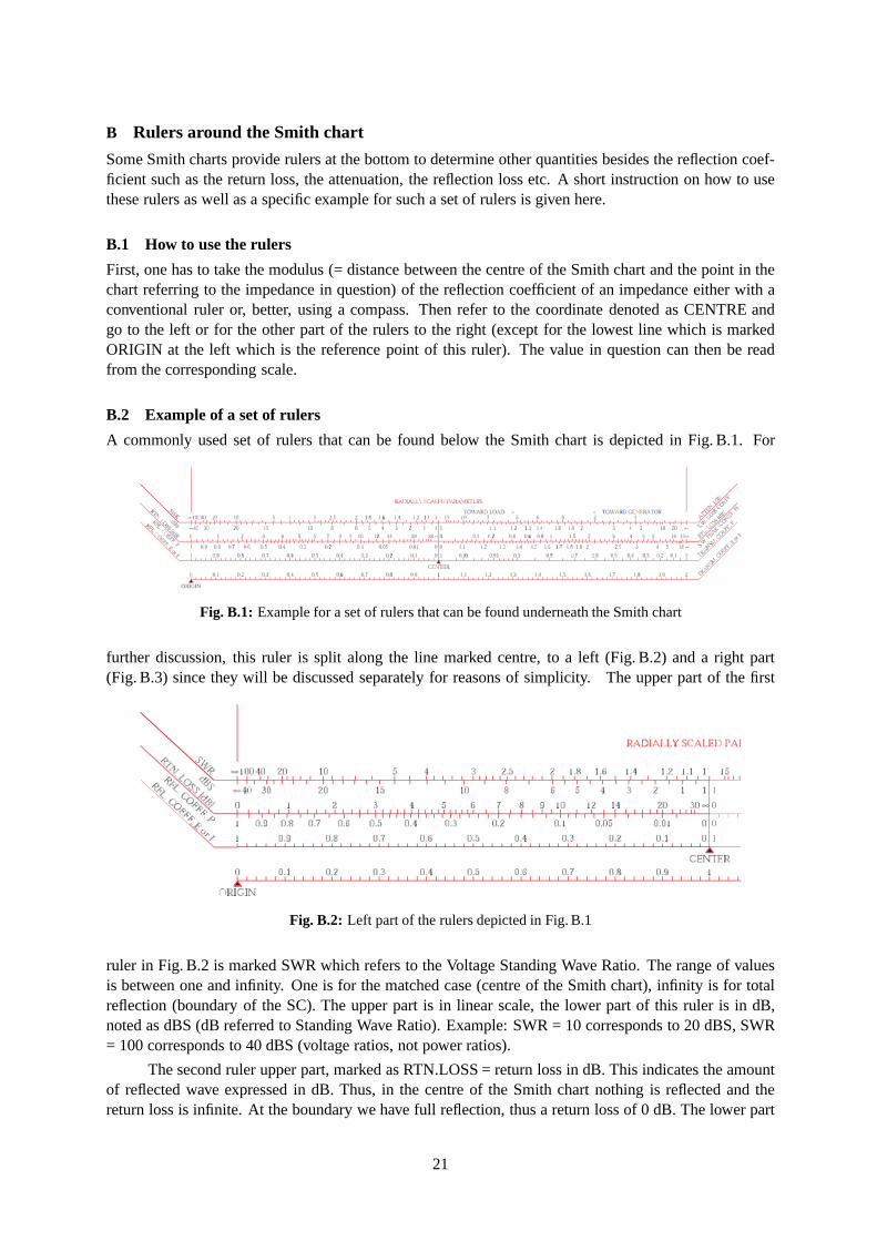
B Rulers around the Smith chart
Some Smith charts provide rulers at the bottom to determine other quantities besides the reflection coef-ficient such as the return loss, the attenuation, the reflection loss etc. A short instruction on how to usethese rulers as well as a specific example for such a set of rulers is given here.
B.1 How to use the rulers
First, one has to take the modulus (= distance between the centre of the Smith chart and the point in thechart referring to the impedance in question) of the reflection coefficient of an impedance either with aconventional ruler or, better, using a compass. Then refer to the coordinate denoted as CENTRE andgo to the left or for the other part of the rulers to the right (except for the lowest line which is markedORIGIN at the left which is the reference point of this ruler). The value in question can then be readfrom the corresponding scale.
B.2 Example of a set of rulers
A commonly used set of rulers that can be found below the Smithchart is depicted in Fig. B.1. For
Fig. B.1: Example for a set of rulers that can be found underneath the Smith chart
further discussion, this ruler is split along the line marked centre, to a left (Fig. B.2) and a right part(Fig. B.3) since they will be discussed separately for reasons of simplicity. The upper part of the first
Fig. B.2: Left part of the rulers depicted in Fig. B.1
ruler in Fig. B.2 is marked SWR which refers to the Voltage Standing Wave Ratio. The range of valuesis between one and infinity. One is for the matched case (centre of the Smith chart), infinity is for totalreflection (boundary of the SC). The upper part is in linear scale, the lower part of this ruler is in dB,noted as dBS (dB referred to Standing Wave Ratio). Example: SWR = 10 corresponds to 20 dBS, SWR= 100 corresponds to 40 dBS (voltage ratios, not power ratios).
The second ruler upper part, marked as RTN.LOSS = return lossin dB. This indicates the amountof reflected wave expressed in dB. Thus, in the centre of the Smith chart nothing is reflected and thereturn loss is infinite. At the boundary we have full reflection, thus a return loss of 0 dB. The lower part
21

Fig. B.3: Right part of the rulers depicted in Fig. B.1
of the scale denoted as RFL.COEFF. P = reflection coefficient in terms of POWER (proportional|Γ|2).There is no reflected power for the matched case (centre of theSmith chart), and a (normalized) reflectedpower = 1 at the boundary.
The third ruler is marked as RFL.COEFF,E or I. With this, the modulus (= absolute value) of thereflection coefficient can be determined in linear scale. Note that since we have the modulus we canrefer it both to voltage or current as we have omitted the sign, we just use the modulus. Obviously in thecentre the reflection coefficient is zero, while at the boundary it is one.
The fourth ruler is the voltage transmission coefficient. Note that the modulus of the voltage (andcurrent) transmission coefficient has a range from zero, i.e., short circuit, to +2 (open = 1+|Γ| with |Γ|=1).This ruler is only valid forZload = real, i.e., the case of a step in characteristic impedance of the coaxialline.
The upper part of the first ruler in Fig. B.3, denoted as ATTEN.in dB assumes that an attenuator(that may be a lossy line) is measured which itself is terminated by an open or short circuit (full reflec-tion). Thus the wave travels twice through the attenuator (forward and backward). The value of thisattenuator can be between zero and some very high number corresponding to the matched case. Thelower scale of this ruler displays the same situation just interms of VSWR. Example: a 10 dB attenuatorattenuates the reflected wave by 20 dB going forth and back andwe get a reflection coefficient ofΓ = 0.1(= 10% in voltage).
The upper part of the second ruler, denoted as RFL.LOSS in dB refers to the reflection loss. Thisis the loss in the transmitted wave, not to be confused with the return loss referring to the reflected wave.It displays the relationPt = 1 − |Γ|2 in dB. Example: If|Γ| = 1/
√2 = 0.707, the transmitted power is
50% and thus the loss is 50% = 3 dB.
The third ruler (right), marked as TRANSM.COEFF.P refers tothe transmitted power as a functionof mismatch and displays essentially the relationPt = 1 − |Γ|2. Thus in the centre of the Smith chartthere is a full match and all the power is transmitted. At the boundary there is total reflection and for aΓvalue of 0.5, for example, 75% of the incident power is transmitted.
References[1] H. Meinke, F.–W. Gundlach, Taschenbuch der Hochfrequenztechnik, Springer Verlag, Berlin, 1992
[2] P. Smith, Electronic Applications of the Smith Chart, Noble Publishing Corporation, 2000
[3] M. Paul, Kreisdiagramme in der Hochfrequenztechnik, R.Oldenburg Verlag, Muenchen, 1969
[4] O. Zinke, H. Brunswig, Lehrbuch der Hochfrequenztechnik, Springer Verlag, Berlin – Heidelberg,1973
22